DESCRIPTIONThe INA152 is a small (MSOP-8), low-power, unity-gain difference amplifier consisting of a CMOS opamp and a precision resistor network. The on-chipresistors are laser trimmed for accurate gain and highcommon-mode rejection. Excellent TCR tracking ofthe resistor maintains gain accuracy and common-mode rejection over temperature. The input common-mode voltage range extends to above the positive and
APPLICATIONS DIFFERENCE INPUT AMPLIFIER
BUILDING BLOCK UNITY-GAIN INVERTING AMPLIFIER GAIN = 1/2 AMPLIFIER GAIN = 2 AMPLIFIER SUMMING AMPLIFIER SYNCHRONOUS DEMODULATOR CURRENT AND DIFFERENTIAL LINE
RECEIVER VOLTAGE-CONTROLLED CURRENT
SOURCE BATTERY-POWERED SYSTEMS LOW-COST AUTOMOTIVE INSTRUMEN-
TATION
negative rails and the output swings to within 50mV ofeither rail.
The difference amplifier is the foundation of manycommonly used circuits. The INA152 provides preci-sion circuit function without using an expensive pre-cision network.
The INA152 is specified for operation over the ex-tended industrial temperature range, –40°C to +85°C.
Input Offset Voltage VCM = 0V ±250 ±1500 µVvs Temperature TA = –40°C to +85°C ±3 ±15 µV/°Cvs Power Supply VS = ±1.35V to ±10V 5 30 µV/Vvs Time 0.5 µV/mo
INPUT VOLTAGE RANGE(3)
Common-Mode Voltage RangeVIN+ – VIN– = 0V 2(V–) 2(V+) – 2 V
OUTPUTVoltage RL = 10kΩ to GND (V+) – 0.35 (V+) – 0.02 V
(V–) + 0.3 (V–) + 0.15 VLoad Capacitance Stability 500 pFShort-Circuit Curent Continuous to Common +7, –12 mA
POWER SUPPLYRated Voltage ±10 VVoltage Range ±1.35 ±10 V
2.7 20 VCurrent, Quiescent IO = 0mA 500 650 µA
TEMPERATURE RANGESpecification –40 +85 °COperating –55 +125 °CθJA, Junction to Ambient 150 °C/W
TA = +25°C, VS = ±10V, RL = 10kΩ connected to ground, and reference pin connected to ground, unless otherwise noted.
NOTES: (1) Referred to output in unity-gain difference configuration. Note that this circuit has a gain of 2 for the op amp’s offset voltage and noise voltage.(2) Includes effects of amplifier’s input bias and offset currents. (3) Limit IIN through 40kΩ resistors to 1mA. (4) 40kΩ resistors are ratio matched but have ±20%absolute value. (5) Includes effects of amplifier’s input current noise and thermal noise contribution of resistor network. (6) Connected as difference amplifier.
INA152 3SBOS184
INA152EA
PARAMETER CONDITIONS MIN TYP MAX UNITS
OFFSET VOLTAGE RTO(1) (2)
Input Offset Voltage VCM = VOUT = 0V ±250 ±1500 µVvs Temperature TA = –40°C ≤ TA ≤ 85°C ±3 ±15 µV/°C
This integrated circuit can be damaged by ESD. Burr-Brownrecommends that all integrated circuits be handled withappropriate precautions. Failure to observe proper handlingand installation procedures can cause damage.
ESD damage can range from subtle performance degradationto complete device failure. Precision integrated circuits maybe more susceptible to damage because very small parametricchanges could cause the device not to meet its publishedspecifications.
Top View MSOP-8
Supply Voltage, V+ to V– .................................................................. +22VSignal Input Terminals .................................................. +20V ContinuousOutput Short-Circuit to GND Duration .................................... ContinuousOperating Temperature .................................................. –55°C to +125°CStorage Temperature ..................................................... –55°C to +125°CJunction Temperature .................................................................... +150°CLead Temperature (soldering, 10s) ............................................... +300°C
ABSOLUTE MAXIMUM RATINGS(1)
PACKAGE SPECIFIEDDRAWING TEMPERATURE PACKAGE ORDERING TRANSPORT
PRODUCT PACKAGE NUMBER RANGE MARKING NUMBER(1) MEDIA
INA152EA MSOP-8 337 –40°C to +85°C B52 INA152EA/250 Tape and Reel" " " " " INA152EA/2K5 Tape and Reel
NOTE: (1) Models with a slash (/) are available only in Tape and Reel in the quantities indicated (e.g., /2K5 indicates 2500 devices per reel). Ordering 2500 piecesof “INA152EA/2K5” will get a single 2500-piece Tape and Reel.
PACKAGE/ORDERING INFORMATION
Ref
VIN–
VIN+
V–
NC
V+
VO
Sense
1
2
3
4
8
7
6
5
INA152
NC = No Internal Connection
NOTES: (1) Referred to output in unity-gain difference configuration. Note that this circuit has a gain of 2 for the op amp’s offset voltage and noise voltage.(2) Includes effects of amplifier’s input bias and offset currents. (3) Limit IIN through 40kΩ resistors to 1mA.
INA1524SBOS184
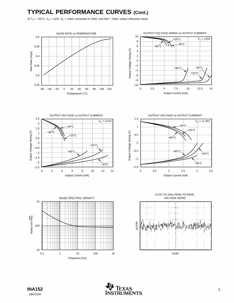
TYPICAL PERFORMANCE CURVESAt TA = +25°C, VS = ±10V, RL = 10kΩ connected to GND, and Ref = GND, unless otherwise noted.
GAIN vs FREQUENCY
Clo
sed-
Loop
Gai
n (d
B)
20
0
–20
–40
–60
–80
Frequency (Hz)
10k 100k 1M 10M
CL = 500pF
COMMON-MODE REJECTION vs FREQUENCY
Com
mom
-Mod
e R
ejec
tion
(dB
)
100
80
60
40
20
Frequency (Hz)
100 1k 10k 100k 1M
VS = ±10V or ±2.5V
POWER-SUPPLY REJECTION vs FREQUENCY
Pow
er-S
uppl
y R
ejec
tion
(dB
)
120
100
80
60
40
20
0
Frequency (Hz)
10 100 1k 10k 100k 1M
+PSRR
–PSRR
MAXIMUM OUTPUT VOLTAGE vs FREQUENCYP
eak-
to-P
eak
Out
put V
olta
ge (
V)
25
20
15
10
5
0
Frequency (Hz)
100 1k 10k 100k 1M
QUIESCENT CURRENT vs TEMPERATURE
Qui
esce
nt C
urre
nt (
µA)
700
600
500
400
300
200
100
0
Temperature (°C)
–75 125–50 –25 0 25 50 75 100
VS = ±10V
VS = ±2.5V
SHORT-CIRCUIT CURRENT vs TEMPERATURE
Sho
rt-C
ircui
t Cur
rent
(m
A)
10
5
0
–5
–10
–15
–20
–25
Temperature (°C)
–60 120–40 –20 0 20 40 60 80 100
VS = ±10V VS = ±2.5V
INA152 5SBOS184
TYPICAL PERFORMANCE CURVES (Cont.)At TA = +25°C, VS = ±10V, RL = 10kΩ connected to GND, and Ref = GND, unless otherwise noted.
0.1Hz TO 10Hz PEAK-TO-PEAKVOLTAGE NOISE
1µV
/div
1s/div
SLEW RATE vs TEMPERATURES
lew
Rat
e (V
/µs)
0.5
0.45
0.4
0.35
0.3
0.25
Temperature (°C)
–60 120–40 –20 0 20 40 60 80 100
OUTPUT VOLTAGE SWING vs OUTPUT CURRENT
Out
put V
olta
ge S
win
g (V
)
10
8
6
4
2
0
–2
–4
–6
–8
–10
Output Current (mA)
0 152.5 5 7.5 10 12.5
VS = ±10V
+85°C–40°C
+25°C
+85°C –40°C
+25°C
OUTPUT VOLTAGE vs OUTPUT CURRENT
Out
put V
olta
ge S
win
g (V
)
2.5
2
1.5
1
0.5
0
–0.5
–1
–1.5
–2
–2.5
Output Current (mA)
0 142 4 6 8 10 12
VS = ±2.5V
+85°C
–40°C
+25°C
+85°C
–40°C
+25°C
OUTPUT VOLTAGE vs OUTPUT CURRENT
Out
put V
olta
ge S
win
g (V
)
1.5
1
0.5
0
–0.5
–1
–1.5
Output Current (mA)
0 2.50.5 1 1.5 2
VS = ±1.35V
+85°C
–40°C
+25°C
+85°C
–40°C
+25°C
NOISE SPECTRAL DENSITY
Noi
se (
nV/√
Hz)
1k
100
10
Frequency (Hz)
0.1 1 10 100 1k
INA1526SBOS184
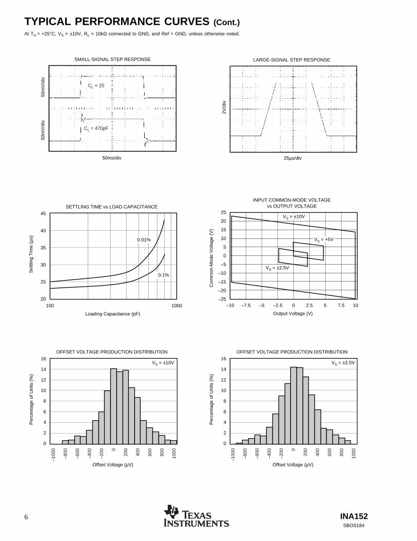
TYPICAL PERFORMANCE CURVES (Cont.)At TA = +25°C, VS = ±10V, RL = 10kΩ connected to GND, and Ref = GND, unless otherwise noted.
LARGE-SIGNAL STEP RESPONSE
2V/d
iv
25µs/div
SETTLING TIME vs LOAD CAPACITANCE
Set
tling
Tim
e (µ
s)
45
40
35
30
25
20
Loading Capacitance (pF)
100 1000
0.01%
0.1%
INPUT COMMON-MODE VOLTAGEvs OUTPUT VOLTAGE
Com
mon
-Mod
e V
olta
ge (
V)
25
20
15
10
5
0
–5
–10
–15
–20
–25
Output Voltage (V)
–10 10–7.5 –5 –2.5 0 2.5 5 7.5
VS = ±10V
VS = +5V
VS = ±2.5V
OFFSET VOLTAGE PRODUCTION DISTRIBUTION
Per
cent
age
of U
nits
(%
)
16
14
12
10
8
6
4
2
0
Offset Voltage (µV)
VS = ±10V
–100
0
–800
–600
–400
–200 0
200
400
600
800
1000
OFFSET VOLTAGE PRODUCTION DISTRIBUTION
Per
cent
age
of U
nits
(%
)
16
14
12
10
8
6
4
2
0
Offset Voltage (µV)
VS = ±2.5V
–100
0
–800
–600
–400
–200 0
200
400
600
800
1000
SMALL-SIGNAL STEP RESPONSE
50m
V/d
iv50
mV
/div
50ms/div
CL = 25
CL = 470pF
INA152 7SBOS184
TYPICAL PERFORMANCE CURVES (Cont.)At TA = +25°C, VS = ±10V, RL = 10kΩ connected to GND, and Ref = GND, unless otherwise noted.
OFFSET VOLTAGE DRIFTP
erce
ntag
e of
Uni
ts (
%)
40
35
30
25
20
15
10
5
0
Offset Voltage Drift (µV/°C)
VS = ±10V
1 2 3 4 5 6 7 8 9 10
OFFSET VOLTAGE DRIFT
Per
cent
age
of U
nits
(%
)
40
35
30
25
20
15
10
5
0
Offset Voltage Drift (µV/°C)
VS = ±2.5V
1 2 3 4 5 6 7 8 9 10
INA1528SBOS184
APPLICATIONS INFORMATIONThe INA152 is a low-power difference amplifier suitable fora wide range of general-purpose applications. Figure 1shows the basic connections required for operation of theINA152. Decoupling capacitors are strongly recommendedin applications with noisy or high-impedance power sup-plies. The capacitors should be placed close to the devicepins, as shown in Figure 1.
As shown in Figure 1, the differential input signal is con-nected to pins 2 and 3. The source impedances connected tothe inputs must be nearly equal to assure good common-mode rejection. An 8Ω mismatch in source impedance willdegrade the common-mode rejection of a typical device toapproximately 80dB (a 16Ω mismatch degrades CMR to74dB). If the source has a known impedance mismatch, anadditional resistor in series with the opposite input can beused to preserve good common-mode rejection.
The INA152’s internal resistors are accurately ratio trimmedto match. That is, R1 is trimmed to match R2, and R3 istrimmed to match R4. However, the absolute values may notbe equal (R1 + R2 may be slightly different than R3 + R4).Thus, large series resistors on the input (greater than 250Ω),even if well matched, will degrade common-mode rejection.
Circuit-board layout constraints might suggest possible varia-tions in connections of the internal resistors. It might appearthat pins 1 and 3 could be interchanged, however, because ofthe ratio trimming technique used (see paragraph above)CMRR will be degraded. If pins 1 and 3 are interchanged,pins 2 and 5 must also be interchanged to maintain properratio matching.
OPERATING VOLTAGE
The INA152 operates from single (+2.7V to +20V) or dual(±1.35V to ±10V) supplies with excellent performance. Speci-fications are production tested with +5V and ±10V supplies.Most behavior remains unchanged throughout the full oper-ating voltage range. Parameters that vary significantly withoperating voltage are shown in the typical performancecurves.
INPUT VOLTAGE
The INA152 can accurately measure differential signals thatare above and below the supply rails. Linear common-moderange extends from 2 • [(V+) – 1V] to 2 • (V–) (nearly twicethe supplies). See the typical performance curve, “InputCommon-Mode Voltage vs Output Voltage”.
OFFSET VOLTAGE TRIM
The INA152 is laser trimmed for low offset voltage and drift.Most applications require no external offset adjustment.Figure 2 shows an optional circuit for trimming the outputoffset voltage. The output is referred to the output referenceterminal (pin 1), which is normally grounded. A voltageapplied to the Ref terminal will be summed with the outputsignal. This can be used to null offset voltage, as shown inFigure 2. The source impedance of a signal applied to the Refterminal should be less than 10Ω to maintain good common-mode rejection.
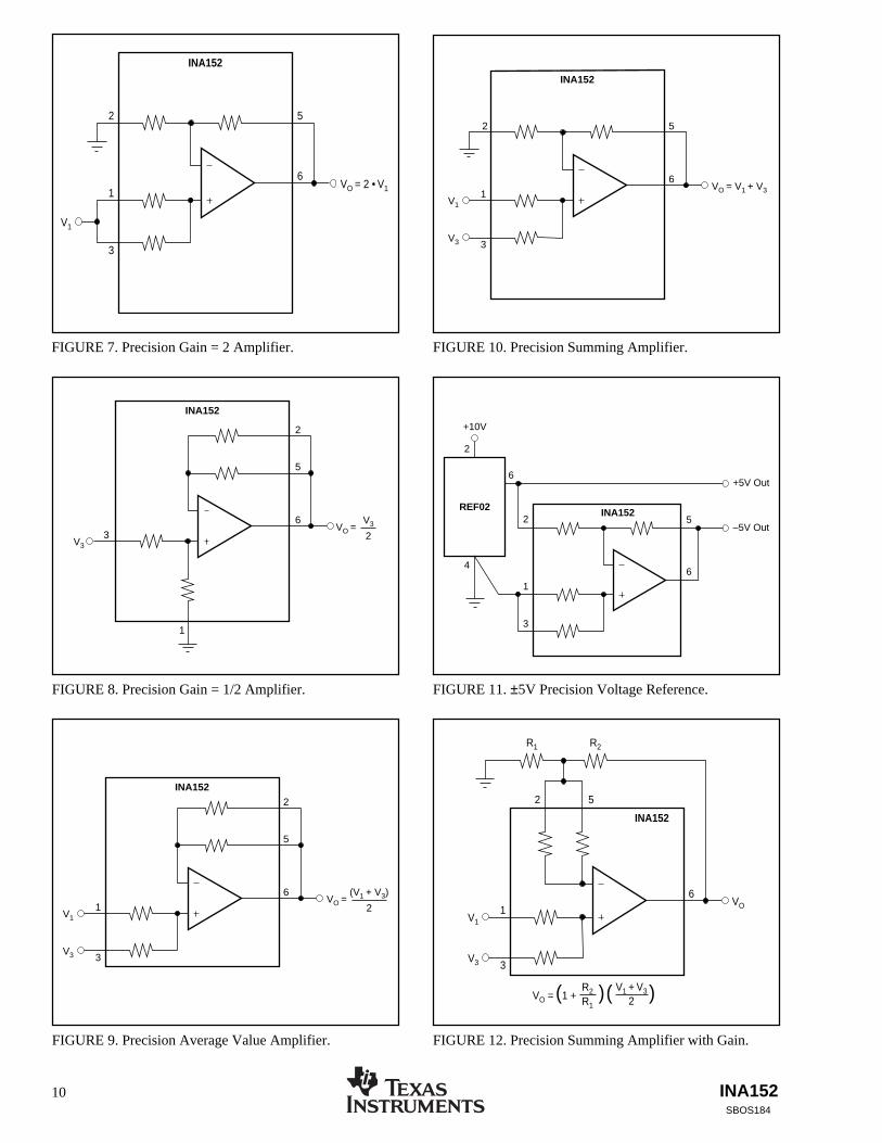
FIGURE 1. Precision Difference Amplifier (Basic PowerSupply and Signal Connections).
The INA152 can be combined with op amps to form a complete Instrumen-tation Amplifier (IA) with specialized performance characteristics. TexasInstruments offers many complete high performance IAs. Products withrelated performances are shown at the right in the table below.
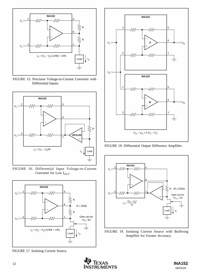
FIGURE 4. Current Receiver with Compliance to Rails.
NOTE: (1) Input series resistors should be less than250Ω (1% max mismatch) to maintain excellent CMR.With 100Ω resistors, gain error is increased to 0.5%.
5
6
2
VO = (V+)/2
INA152
V+
1
7
4
V+
CommonCommon
3
5
6VO = –V2
INA152
2V2
1 3
SIMILAR COMPLETEA1, A2 FEATURE TEXAS INSTRUMENTS IA
FIGURE 19. Isolating Current Source with BufferingAmplifier for Greater Accuracy.
5
6
3
INA1522
1V1
V2
LoadIO = (V1 – V2) (1/40k + 1/R)
IO
R
R
5
6
3
INA152
2
1V3
V2
LoadIO = (V3 – V2)/R
IO
R
OPA130
5
6
3
INA152
2
1V3
V2
Load IO
R
R
Gate can be+VS –5V
IO = (V3 – V2) (1/40k + 1/R)
R < 200Ω
5
6
3
INA152
2
V01
1
5
6
3
INA152
A
B
2
V01 – V02 = 2 (V2 – V1)
V02
1
V2
V1
5
6
3
INA1522
1V3
V2
Load IO
R
Gate can be+VCC –5V
IO =(V3 – V2)
R
(R ≥ 200Ω)
INA152 13SBOS184
FIGURE 23. High Output Current Precision DifferenceAmplifier.
FIGURE 20. Differential Input Data Acquisition.
FIGURE 21. Digitally Controlled Gain of ±1 Amplifier.
FIGURE 22. Precision Absolute Value Buffer.
5
6
1
INA152
ADS7806
2
3
4
7
+5V
VS
12 BitsOut
0V-4VInput
Transduceror
AnalogSignal
–5V
Eliminates errors due to different grounds.
5
6
3
1
INA152
2
1
VO
DG188
V1
LogicIn
Logic In
0
1
VO
–V1
+V1
V1Input
5
6
3
1
V0 = |V1|
INA152
2
R4
R3
R1 R2
OPA130
10pFD1
D2
R52kΩ
5
6
1
INA152
BUF634
2
3
VO
RL
–In
+In
BUF634 inside feedback loop contributes no error.
PACKAGE OPTION ADDENDUM
www.ti.com 18-Oct-2013
Addendum-Page 1
PACKAGING INFORMATION
Orderable Device Status(1)
Package Type PackageDrawing
Pins PackageQty
Eco Plan(2)
Lead/Ball Finish(6)
MSL Peak Temp(3)
Op Temp (°C) Device Marking(4/5)
Samples
INA152EA/250 ACTIVE VSSOP DGK 8 250 Green (RoHS& no Sb/Br)
CU NIPDAU |CU NIPDAUAG
Level-3-260C-168 HR -40 to 85 B52
INA152EA/250G4 ACTIVE VSSOP DGK 8 250 Green (RoHS& no Sb/Br)
CU NIPDAU Level-3-260C-168 HR -40 to 85 B52
INA152EA/2K5 ACTIVE VSSOP DGK 8 2500 Green (RoHS& no Sb/Br)
CU NIPDAU |CU NIPDAUAG
Level-3-260C-168 HR -40 to 85 B52
INA152EA/2K5G4 ACTIVE VSSOP DGK 8 2500 Green (RoHS& no Sb/Br)
CU NIPDAU Level-3-260C-168 HR -40 to 85 B52
(1) The marketing status values are defined as follows:ACTIVE: Product device recommended for new designs.LIFEBUY: TI has announced that the device will be discontinued, and a lifetime-buy period is in effect.NRND: Not recommended for new designs. Device is in production to support existing customers, but TI does not recommend using this part in a new design.PREVIEW: Device has been announced but is not in production. Samples may or may not be available.OBSOLETE: TI has discontinued the production of the device.
(2) Eco Plan - The planned eco-friendly classification: Pb-Free (RoHS), Pb-Free (RoHS Exempt), or Green (RoHS & no Sb/Br) - please check http://www.ti.com/productcontent for the latest availabilityinformation and additional product content details.TBD: The Pb-Free/Green conversion plan has not been defined.Pb-Free (RoHS): TI's terms "Lead-Free" or "Pb-Free" mean semiconductor products that are compatible with the current RoHS requirements for all 6 substances, including the requirement thatlead not exceed 0.1% by weight in homogeneous materials. Where designed to be soldered at high temperatures, TI Pb-Free products are suitable for use in specified lead-free processes.Pb-Free (RoHS Exempt): This component has a RoHS exemption for either 1) lead-based flip-chip solder bumps used between the die and package, or 2) lead-based die adhesive used betweenthe die and leadframe. The component is otherwise considered Pb-Free (RoHS compatible) as defined above.Green (RoHS & no Sb/Br): TI defines "Green" to mean Pb-Free (RoHS compatible), and free of Bromine (Br) and Antimony (Sb) based flame retardants (Br or Sb do not exceed 0.1% by weightin homogeneous material)
(3) MSL, Peak Temp. - The Moisture Sensitivity Level rating according to the JEDEC industry standard classifications, and peak solder temperature.
(4) There may be additional marking, which relates to the logo, the lot trace code information, or the environmental category on the device.
(5) Multiple Device Markings will be inside parentheses. Only one Device Marking contained in parentheses and separated by a "~" will appear on a device. If a line is indented then it is a continuationof the previous line and the two combined represent the entire Device Marking for that device.
(6) Lead/Ball Finish - Orderable Devices may have multiple material finish options. Finish options are separated by a vertical ruled line. Lead/Ball Finish values may wrap to two lines if the finishvalue exceeds the maximum column width.
Important Information and Disclaimer:The information provided on this page represents TI's knowledge and belief as of the date that it is provided. TI bases its knowledge and belief on informationprovided by third parties, and makes no representation or warranty as to the accuracy of such information. Efforts are underway to better integrate information from third parties. TI has taken andcontinues to take reasonable steps to provide representative and accurate information but may not have conducted destructive testing or chemical analysis on incoming materials and chemicals.TI and TI suppliers consider certain information to be proprietary, and thus CAS numbers and other limited information may not be available for release.
In no event shall TI's liability arising out of such information exceed the total purchase price of the TI part(s) at issue in this document sold by TI to Customer on an annual basis.
Texas Instruments Incorporated and its subsidiaries (TI) reserve the right to make corrections, enhancements, improvements and otherchanges to its semiconductor products and services per JESD46, latest issue, and to discontinue any product or service per JESD48, latestissue. Buyers should obtain the latest relevant information before placing orders and should verify that such information is current andcomplete. All semiconductor products (also referred to herein as “components”) are sold subject to TI’s terms and conditions of salesupplied at the time of order acknowledgment.
TI warrants performance of its components to the specifications applicable at the time of sale, in accordance with the warranty in TI’s termsand conditions of sale of semiconductor products. Testing and other quality control techniques are used to the extent TI deems necessaryto support this warranty. Except where mandated by applicable law, testing of all parameters of each component is not necessarilyperformed.
TI assumes no liability for applications assistance or the design of Buyers’ products. Buyers are responsible for their products andapplications using TI components. To minimize the risks associated with Buyers’ products and applications, Buyers should provideadequate design and operating safeguards.
TI does not warrant or represent that any license, either express or implied, is granted under any patent right, copyright, mask work right, orother intellectual property right relating to any combination, machine, or process in which TI components or services are used. Informationpublished by TI regarding third-party products or services does not constitute a license to use such products or services or a warranty orendorsement thereof. Use of such information may require a license from a third party under the patents or other intellectual property of thethird party, or a license from TI under the patents or other intellectual property of TI.
Reproduction of significant portions of TI information in TI data books or data sheets is permissible only if reproduction is without alterationand is accompanied by all associated warranties, conditions, limitations, and notices. TI is not responsible or liable for such altereddocumentation. Information of third parties may be subject to additional restrictions.
Resale of TI components or services with statements different from or beyond the parameters stated by TI for that component or servicevoids all express and any implied warranties for the associated TI component or service and is an unfair and deceptive business practice.TI is not responsible or liable for any such statements.
Buyer acknowledges and agrees that it is solely responsible for compliance with all legal, regulatory and safety-related requirementsconcerning its products, and any use of TI components in its applications, notwithstanding any applications-related information or supportthat may be provided by TI. Buyer represents and agrees that it has all the necessary expertise to create and implement safeguards whichanticipate dangerous consequences of failures, monitor failures and their consequences, lessen the likelihood of failures that might causeharm and take appropriate remedial actions. Buyer will fully indemnify TI and its representatives against any damages arising out of the useof any TI components in safety-critical applications.
In some cases, TI components may be promoted specifically to facilitate safety-related applications. With such components, TI’s goal is tohelp enable customers to design and create their own end-product solutions that meet applicable functional safety standards andrequirements. Nonetheless, such components are subject to these terms.
No TI components are authorized for use in FDA Class III (or similar life-critical medical equipment) unless authorized officers of the partieshave executed a special agreement specifically governing such use.
Only those TI components which TI has specifically designated as military grade or “enhanced plastic” are designed and intended for use inmilitary/aerospace applications or environments. Buyer acknowledges and agrees that any military or aerospace use of TI componentswhich have not been so designated is solely at the Buyer's risk, and that Buyer is solely responsible for compliance with all legal andregulatory requirements in connection with such use.
TI has specifically designated certain components as meeting ISO/TS16949 requirements, mainly for automotive use. In any case of use ofnon-designated products, TI will not be responsible for any failure to meet ISO/TS16949.
Products Applications
Audio www.ti.com/audio Automotive and Transportation www.ti.com/automotive
Amplifiers amplifier.ti.com Communications and Telecom www.ti.com/communications
Data Converters dataconverter.ti.com Computers and Peripherals www.ti.com/computers