+ All Categories
Home > Documents > Sleepy stack: a New Approach to Low Power VLSI Logic and Memory

Sleepy stack: a New Approach to Low Power VLSI Logic and Memory

Date post: 03-Feb-2022
Category:
Upload: others
View: 7 times
Download: 0 times
Share this document with a friend
61
Sleepy stack: a New Approach to Low Power VLSI Logic and Memory Ph.D. Dissertation Defense by Jun Cheol Park Advisor: Vincent J. Mooney III School of Electrical and Computer Engineering Georgia Institute of Technology June 2005 © 2005 Georgia Institute of Technology
Transcript

Sleepy stack: a New Approach to Low Power VLSI Logic and Memory

Ph.D. Dissertation Defenseby

Jun Cheol ParkAdvisor: Vincent J. Mooney III

School of Electrical and Computer EngineeringGeorgia Institute of Technology

June 2005

© 2005 Georgia Institute of Technology

© 2005 Georgia Institute of Technology 2

Outline

IntroductionRelated WorkSleepy stack Sleepy stack logic circuitsSleepy stack SRAMLow-power pipelined cache (LPPC)Sleepy stack pipelined SRAMConclusion

© 2005 Georgia Institute of Technology 3

Power consumption

Power consumption of VLSI is a fundamental problem of mobile devices as well high-performance computers

Limited operation (battery life)HeatOperation cost

Power = dynamic + static Dynamic power more than 90% of total power (0.18u tech. and above)

Dynamic power reduction: Technology scalingFrequency scalingVoltage scaling IBM PowerPC 970*

*N. Rohrer et al., “PowerPC 970 in 130nm and 90nm Technologies," IEEE International Solid-State circuits Conference, vol 1, pp. 68-69, February 2004.

© 2005 Georgia Institute of Technology 4

MotivationUltra-low leakage power

A cell phone calling plan with 500min (per month 43,200min)Leakage reduction technique can potentially increase battery life 34X

State-saving Prior ultra-low-leakage techniques (e.g., sleep transistor) lose logic state thus requires long wake-up timeUsers can use a cell phone without waiting long wake-up time

Emergency calling situation

Power consumption scenariofor 0.07u tech, processor

*Assume chip area ½ processor logic and ½ memory, no on-chip memory, leakage power matches to dynamic power at 0.07u tech.

Active (W) Leakeage (W) Energy (J)(Month) Active (W) Leakage (W) Energy (J)

(Month)Proc. 1.71E-01 1.34E-01 3.49E+05 1.82E-01 7.57E-04 7.39E+03

32KB SRAM 3.83E-02 6.99E-02 1.80E+05 4.10E-02 2.74E-03 8.26E+03Total 2.09E-01 2.04E-01 5.30E+05 2.23E-01 3.50E-03 1.56E+04

Best prior work(forced stack)

Our approach(sleepy stack)

© 2005 Georgia Institute of Technology 5

Leakage power

Leakage power became important as the feature size shrinksSubthreshold leakage

Scaling down of Vth: Leakage increases exponentially as VthdecreasesShort-channel effect: channel controlled by drainOur research focus

Gate-oxide leakageGate tunneling due to thin oxideHigh-k dielectric could be a solution

n+ n+

DrainSource

Gate

P-substrate

SubthresholdLeakage current

Gate-oxideLeakage current

NFET

*Berkeley Predictive Technology Model (BPTM). [Online]. Available http://www-device.eecs.berkeley.edu/~ptm.

1.00E-10

1.00E-09

1.00E-08

1.00E-07

1.00E-06

1.00E-05

1.00E-040.18u 0.13u 0.10u 0.07u

Dynamic Power Leakage Power

Experimental result 4-bit adder*

© 2005 Georgia Institute of Technology 6

Contribution

Design of novel ultra-low leakage sleepy stack which savies stateDesign of sleepy stack SRAM cell which provides new pareto points in ultra-low leakage power consumption Design of low-power pipelined cache and find optimal number of pipeline stages in the given architectureDesign of sleepy stack pipelined SRAM for low-leakage

© 2005 Georgia Institute of Technology 7

Outline

IntroductionRelated WorkSleepy stack Sleepy stack logic circuitsSleepy stack SRAMLow-power pipelined cache (LPPC)Sleepy stack pipelined SRAMConclusion

© 2005 Georgia Institute of Technology 8

Low-leakage CMOS VLSI

LogicNetwork

Sleep transistor

Sleep transistorMulti-threshold-voltage CMOS (MTCMOS) [Mutoh95]Loses state and incurs high wake-up cost

Zigzag [Min03]Non-floating by asserting a predefined input during sleep mode Only retain predefined state

Stack [Narendra01]Stack effect: when two or more stacked transistors turned off together, leakage power is suppressedForcing stackCannot utilize high-Vth without huge delay penalties (>6.2X) (we will show for less, e.g., 2.8X)

© 2005 Georgia Institute of Technology 9

Low-leakage CMOS VLSI

PullupNetwork

A

PulldownNetwork

B

PullupNetwork

A

PulldownNetwork

B

PullupNetwork

A

PulldownNetwork

B

S’

S

S’

Zigzag

1010

Sleep transistorMulti-threshold-voltage CMOS (MTCMOS) [Mutoh95]Loses state and incurs high wake-up cost

Zigzag [Min03]Non-floating by asserting a predefined input during sleep mode Only retain predefined state

Stack [Narendra01]Stack effect: when two or more stacked transistors turned off together, leakage power is suppressedForcing stackCannot utilize high-Vth without huge delay penalties (>6.2X) (we will show for less, e.g., 2.8X)

© 2005 Georgia Institute of Technology 10

Low-leakage CMOS VLSI

Forcing stack

4

2

2

2

1

1

Sleep transistorMulti-threshold-voltage CMOS (MTCMOS) [Mutoh95]Loses state and incurs high wake-up cost

Zigzag [Min03]Non-floating by asserting a predefined input during sleep mode Only retain predefined state

Stack [Narendra01]Stack effect: when two or more stacked transistors turned off together, leakage power is suppressedForcing stackCannot utilize high-Vth without huge delay penalties (>6.2X) (we will show for less, e.g., 2.8X)

© 2005 Georgia Institute of Technology 11

Low-leakage CMOS VLSI comparison summary

Sleepy stack approaches for logic circuitsSaves exact state, so does not need to restore original state (unlike the sleep transistor technique and the zigzag technique)Larger leakage power saving (forced stack)

© 2005 Georgia Institute of Technology 12

Auto-Backgate-Controlled Multi Threshold CMOS (ABC-MTCMOS) [Nii98]

Reverse source-body bias during sleep modeSlow transition and large dynamic power to charge n-wells

Gated-Vdd [Powell00](Prof. K. Roy)Isolate SRAM cells using sleep transistorLoses state during sleep mode

Drowsy cache [Flautner02]Scaling Vdd dynamicallySmaller leakage reduction (<86%) (we will show 3 orders magnitude reduction)

n-well

DrainSourceGate

p-substrate

ABC-MTCMOS

p+ p+

Vdd High-Vdd

Low-leakage SRAM

© 2005 Georgia Institute of Technology 13

Low-leakage SRAM

Gated-VDDcontrol

wordline

VDD

bitlinebitline’

VGND

Gated-VDD

*Intel introduces 65-nm sleep transistor SRAMfrom Intel.com , “65-nm process technology extends the benefit of Moore’s law”

Auto-Backgate-Controlled Multi Threshold CMOS (ABC-MTCMOS) [Nii98]

Reverse source-body bias during sleep modeSlow transition and large dynamic power to charge n-wells

Gated-Vdd [Powell00](Prof. K. Roy)Isolate SRAM cells using sleep transistorLoses state during sleep mode

Drowsy cache [Flautner02]Scaling Vdd dynamicallySmaller leakage reduction (<86%) (we will show 3 orders magnitude reduction)

© 2005 Georgia Institute of Technology 14

Low-leakage SRAM

Drowsy cache

P1

bit

wordline

bit’

P2

N1N2

N3N4

VDDH

VDDL

LowVolt

LowVolt’

Auto-Backgate-Controlled Multi Threshold CMOS (ABC-MTCMOS) [Nii98]

Reverse source-body bias during sleep modeSlow transition and large dynamic power to charge n-wells

Gated-Vdd [Powell00](Prof. K. Roy)Isolate SRAM cells using sleep transistorLoses state during sleep mode

Drowsy cache [Flautner02]Scaling Vdd dynamicallySmaller leakage reduction (<86%) (we will show 3 orders magnitude reduction)

© 2005 Georgia Institute of Technology 15

Low-power pipelined cache

Breaking down a cache into multiple segment cache can be pipelined to increase performance [Chappell91][Agarwal03]

No power reduction addressedPipelining caches to offset performance degradation and pipelined cache [Gunadi04]

Saving power by enabling necessary subbankOnly dynamic power is addresses (0.18u technology)

© 2005 Georgia Institute of Technology 16

Low-leakage SRAM and low power cache comparison

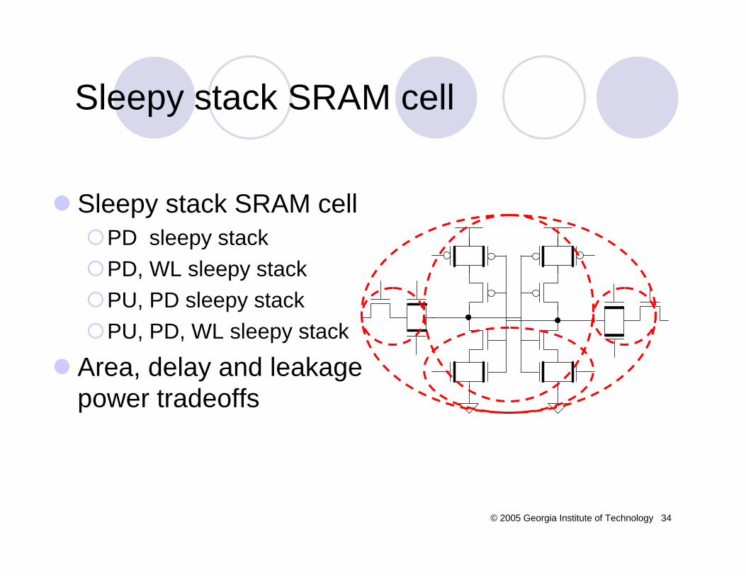
Sleepy stack SRAM cellNo need to charge n-well (ABC-MTCMOS)State-saving (gated-Vdd)

Larger leakage power savings (drowsy cache)No prior work found that uses a pipelined cache to reduce dynamic power by scaling Vdd or reducing static power

© 2005 Georgia Institute of Technology 17

Outline

IntroductionRelated WorkSleepy stackSleepy stack logic circuitsSleepy stack SRAMLow-power pipelined cache (LPPC)Sleepy stack pipelined SRAMConclusion

© 2005 Georgia Institute of Technology 18

Introduction of sleepy stack

New state-saving ultra low-leakage technique Combination of the sleep transistor and forced stack techniqueApplicable to generic VLSI structures as well as SRAMTarget application requires long standby with fast response, e.g., cell phone

© 2005 Georgia Institute of Technology 19

stack inverter

W/L=1.5

W/L=1.5

W/L=3

W/L=3

W/L=1.5

W/L=3

S’

S

Sleepy stack inverter

Sleepy stack structure

First, Break down a transistor similar to the forced stack technique Then add sleep transistors

W/L=3

W/L=6

Conventional CMOS inverter

© 2005 Georgia Institute of Technology 20

Sleepy stack operation

During active mode, sleep transistors are on, then reduced resistance increases current while reducing delayDuring sleep mode, sleep transistors are off, stacked transistors suppress leakage current while saving stateCan apply high-Vth, which is not used in the forced stack technique due to the dramatic delay increase (>6.2X)

W/L=1.5

W/L=1.5 W/L=1.5

S’=1

W/L=3

W/L=3W/L=3

S=0

S’=0

S=1On

On Off

Off

Active mode Sleep mode

Stack effect

Stack effect Low-Vth

High-Vth

© 2005 Georgia Institute of Technology 21

Outline

IntroductionRelated WorkSleepy stack Sleepy stack logic circuitsSleepy stack SRAMLow-power pipelined cache (LPPC)Sleepy stack pipelined SRAMConclusion

© 2005 Georgia Institute of Technology 22

Experimental methodology

Five techniques are comparedbase case, forced stack, sleep*, zigzag* and sleepy stack* (*single- and dual-Vth applied)

Three benchmark circuits are used (CL=3Cinv)A chain of 4 inverters

4 inverter chainCin=3Cinv, CL=3Cinv

4:1 multiplexer5 stagesstandard cell gatesCin=11Cinv, CL=3Cinv

4-bit adder4 full adders complex gateCin=18.5Cinv, CL=3Cinv

© 2005 Georgia Institute of Technology 23

Experimental methodology

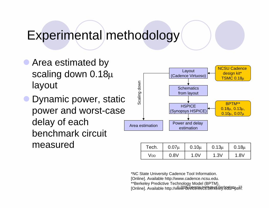
Area estimated by scaling down 0.18µlayoutDynamic power, static power and worst-case delay of each benchmark circuit measured

Layout(Cadence Virtuoso)

Schematicsfrom layout

HSPICE(Synopsys HSPICE)

Power and delay estimationArea estimation

Scal

ing

dow

n

NCSU Cadence design kit*

TSMC 0.18µ

BPTM**0.18µ, 0.13µ,0.10µ, 0.07µ

0.8V

0.07µ

1.8V

0.18µ

1.0V

0.10µ

1.3V

0.13µ

VDD

Tech.

*NC State University Cadence Tool Information. [Online]. Available http://www.cadence.ncsu.edu.**Berkeley Predictive Technology Model (BPTM). [Online]. Available http://www-device.eecs.berkeley.edu/~ptm.

© 2005 Georgia Institute of Technology 24

A chain of 4 inverters * Dual-Vth applied (0.2V and 0.4V)

1.E-16

1.E-15

1.E-14

1.E-13

1.E-12

1.E-11

1.E-10

1.E-09

1.E-08

1.E-07

Base c

ase

Stack

Sleep

ZigZag

Sleepy

Stack

Sleep*

ZigZag

*Slee

py Stac

k*

TSMC 0.18u

Berkeley 0.18u

Berkeley 0.13u

Berkeley 0.10u

Berkeley 0.07u1.E-07

1.E-06

1.E-05

1.E-04

Base c

ase

Stack

Sleep

ZigZag

Sleepy

Stack

Sleep*

ZigZag

*Slee

py Stac

k*

(a) Static power (W) (b) Dynamic power (W)

0.0E+00

5.0E-11

1.0E-10

1.5E-10

2.0E-10

2.5E-10

3.0E-10

Base c

ase

Stack

Sleep

ZigZag

Sleepy

Stack

Sleep*

ZigZag

*Slee

py Stac

k*

(c) Propagation delay (s) (d) Area (µ2)

1

10

100

Base c

ase

Stack

Sleep

ZigZag

Sleepy

Stack

Sleep*

ZigZag

*Slee

py Stac

k*

© 2005 Georgia Institute of Technology 25

A chain of 4 inverters

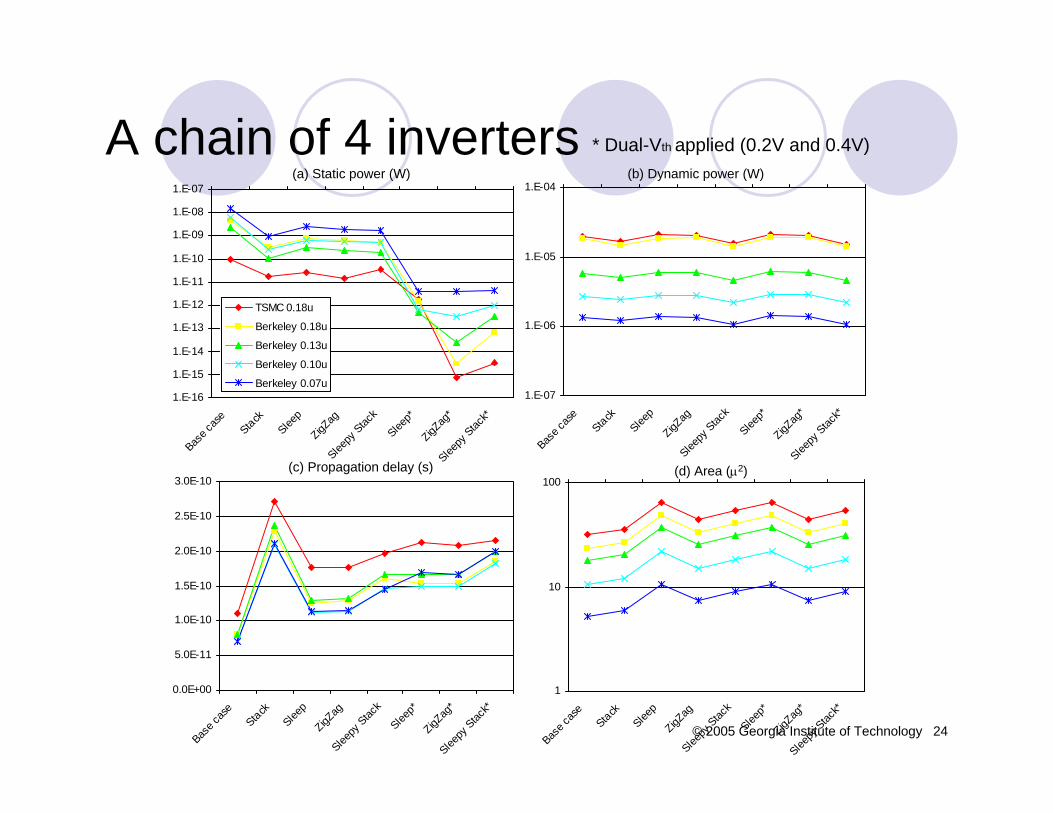
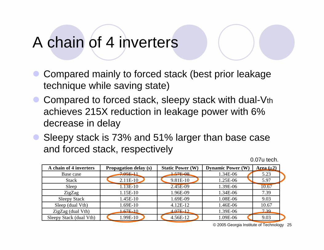
Compared mainly to forced stack (best prior leakage technique while saving state)Compared to forced stack, sleepy stack with dual-Vthachieves 215X reduction in leakage power with 6% decrease in delaySleepy stack is 73% and 51% larger than base case and forced stack, respectively

A chain of 4 inverters Propagation delay (s) Static Power (W) Dynamic Power (W) Area (µ2)Base case 7.05E-11 1.57E-08 1.34E-06 5.23

Stack 2.11E-10 9.81E-10 1.25E-06 5.97Sleep 1.13E-10 2.45E-09 1.39E-06 10.67

ZigZag 1.15E-10 1.96E-09 1.34E-06 7.39Sleepy Stack 1.45E-10 1.69E-09 1.08E-06 9.03

Sleep (dual Vth) 1.69E-10 4.12E-12 1.46E-06 10.67ZigZag (dual Vth) 1.67E-10 4.07E-12 1.39E-06 7.39

Sleepy Stack (dual Vth) 1.99E-10 4.56E-12 1.09E-06 9.03

0.07u tech.

© 2005 Georgia Institute of Technology 26

4:1 Multiplexer

1.E-12

1.E-11

1.E-10

1.E-09

1.E-08

1.E-07

1.E-06

Base c

ase

Stack

Sleep

ZigZag

Sleepy

Stack

Sleep*

ZigZag

*Slee

py Stac

k*

TSMC 0.18u

Berkeley 0.18u

Berkeley 0.13u

Berkeley 0.10u

Berkeley 0.07u

1.E-06

1.E-05

1.E-04

Base c

ase

Stack

Sleep

ZigZag

Sleepy

Stack

Sleep*

ZigZag

*Slee

py Stac

k*

(a) Static power (W) (b) Dynamic power (W)

0.0E+00

1.0E-10

2.0E-10

3.0E-10

4.0E-10

5.0E-10

6.0E-10

7.0E-10

8.0E-10

Base c

ase

Stack

Sleep

ZigZag

Sleepy

Stack

Sleep*

ZigZag

*Slee

py Stac

k*

(c) Propagation delay (s) (d) Area (µ2)

10

100

1000

Base c

ase

Stack

Sleep

ZigZag

Sleepy

Stack

Sleep*

ZigZag

*Slee

py Stac

k*

* Dual-Vth applied (0.2V and 0.4V)

© 2005 Georgia Institute of Technology 27

4:1 Multiplexer

Compared to forced stack, sleepy stack with dual-Vth achieves 202X reduction in leakage power with 7% increase in delaySleepy stack is 150% and 118% larger than base case and forced stack, respectively

4:1 multiplexer Propagation delay (s) Static Power (W) Dynamic Power (W) Area (µ2)Base case 1.39E-10 8.57E-08 2.49E-06 50.17

Stack 4.52E-10 6.46E-09 2.14E-06 57.40Sleep 1.99E-10 1.65E-08 2.10E-06 74.11

ZigZag 2.17E-10 1.36E-08 2.54E-06 74.36Sleepy Stack 3.35E-10 1.09E-08 2.18E-06 125.33

Sleep (dual Vth) 2.87E-10 2.41E-11 2.15E-06 74.11ZigZag (dual Vth) 3.28E-10 3.62E-11 2.59E-06 74.36

Sleepy Stack (dual Vth) 4.84E-10 3.20E-11 2.09E-06 125.33

0.07u tech.

© 2005 Georgia Institute of Technology 28

4-bit adder

1.E-12

1.E-11

1.E-10

1.E-09

1.E-08

1.E-07

1.E-06

Base c

ase

Stack

Sleep

ZigZag

Sleepy

Stack

Sleep*

ZigZag

*Slee

py Stac

k*

TSMC 0.18u

Berkeley 0.18u

Berkeley 0.13u

Berkeley 0.10u

Berkeley 0.07u

1.E-06

1.E-05

1.E-04

1.E-03

Base c

ase

Stack

Sleep

ZigZag

Sleepy

Stack

Sleep*

ZigZag

*Slee

py Stac

k*

(a) Static power (W) (b) Dynamic power (W)

0.0E+00

2.0E-10

4.0E-10

6.0E-10

8.0E-10

1.0E-09

1.2E-09

1.4E-09

1.6E-09

1.8E-09

Base c

ase

Stack

Sleep

ZigZag

Sleepy

Stack

Sleep*

ZigZag

*Slee

py Stac

k*

(c) Propagation delay (s) (d) Area (µ2)

10

100

1000

Base c

ase

Stack

Sleep

ZigZag

Sleepy

Stack

Sleep*

ZigZag

*Slee

py Stac

k*

* Dual-Vth applied (0.2V and 0.4V)

© 2005 Georgia Institute of Technology 29

4-bit adder

Compared to forced stack, sleepy stack with dual-Vth achieves 190X reduction in leakage power with 6% increase in delaySleepy stack is 187% and 113% larger than base case and forced stack, respectively

4-bit adder Propagation delay (s) Static Power (W) Dynamic Power (W) Area (µ2)Base case 3.76E-10 8.87E-08 8.81E-06 22.96

Stack 1.16E-09 6.77E-09 7.63E-06 30.94Sleep 5.24E-10 1.24E-08 9.03E-06 30.94

ZigZag 5.24E-10 9.09E-09 8.44E-06 27.62Sleepy Stack 8.65E-10 1.07E-08 7.70E-06 65.88

Sleep (dual Vth) 7.48E-10 2.23E-11 9.41E-06 30.94ZigZag (dual Vth) 7.43E-10 2.19E-11 8.53E-06 27.62

Sleepy Stack (dual Vth) 1.23E-09 3.56E-11 7.26E-06 65.88

0.07u tech

© 2005 Georgia Institute of Technology 30

Sleepy stack Vth variation

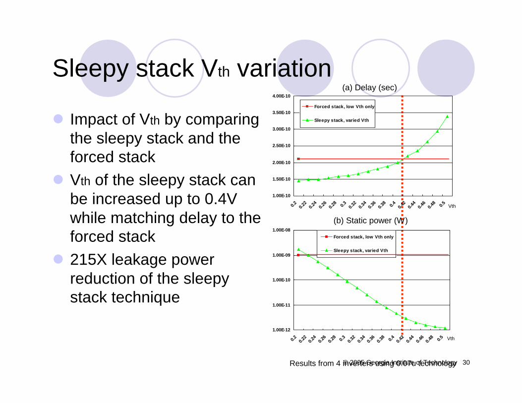
Impact of Vth by comparing the sleepy stack and the forced stackVth of the sleepy stack can be increased up to 0.4V while matching delay to the forced stack215X leakage power reduction of the sleepy stack technique

Results from 4 inverters using 0.07u technology

(a) Delay (sec)

1.00E-12

1.00E-11

1.00E-10

1.00E-09

1.00E-080.2 0.2

20.2

40.2

60.2

8 0.3 0.32

0.34

0.36

0.38 0.4 0.42

0.44

0.46

0.48 0.5

Forced stack, low Vth only

Sleepy stack, varied Vth

1.00E-10

1.50E-10

2.00E-10

2.50E-10

3.00E-10

3.50E-10

4.00E-10

0.2 0.22

0.24

0.26

0.28 0.3 0.32

0.34

0.36

0.38 0.4 0.42

0.44

0.46

0.48 0.5

Forced stack, low Vth only

Sleepy stack, varied Vth

(b) Static power (W)

Vth

Vth

© 2005 Georgia Institute of Technology 31

Forced stack transistorwidth variation

Impact of the forced stack transistor width by comparing the sleepy stack and the forced stack using similar areaForced stack Vth=0.2V, sleepy stack (sleep and paralleled transistor) Vth=0.4VBetween 2X~2.5X transistor width of the forced stack matches area with the sleepy stackForce stack is 1.5% faster but leakage power is 430X larger

Results from 4 inverters using 0.07u technology

(b) Delay (sec)

1.60E-10

1.70E-10

1.80E-10

1.90E-10

2.00E-10

2.10E-10

2.20E-10

1 1.5 2 2.5 3 3.5 4 4.5 5

Forced stack, varied w idth

Sleepy stack, f ixed w idth

(c) Static power (W)

1.00E-12

1.00E-11

1.00E-10

1.00E-09

1.00E-08

1.00E-07

1 1.5 2 2.5 3 3.5 4 4.5 5

Forced stack, varied w ithSleepy stack, f ixed w idth

20

30

40

50

60

70

80

1 1.5 2 2.5 3 3.5 4 4.5 5

Forced stack, varied w idth

Sleepy stack, f ixed w idth

(a) Area (u2)

xWidth

xWidth

xWidth

© 2005 Georgia Institute of Technology 32

Outline

IntroductionRelated WorkSleepy stack Sleepy stack logic circuitsSleepy stack SRAMLow-power pipelined cache (LPPC)Sleepy stack pipelined SRAMConclusion

© 2005 Georgia Institute of Technology 33

Sleepy stack SRAM cellSleepy stack technique achieves ultra-low leakage power while saving stateApply the sleepy stack technique to SRAM cell design

Large leakage power saving expected in cacheState-saving6-T SRAM cell is based on coupled inverters

SRAM cell leakage pathsCell leakage Bitline leakage

© 2005 Georgia Institute of Technology 34

Sleepy stack SRAM cell

Sleepy stack SRAM cellPD sleepy stackPD, WL sleepy stackPU, PD sleepy stackPU, PD, WL sleepy stack

Area, delay and leakage power tradeoffs

© 2005 Georgia Institute of Technology 35

Experimental methodology

Base case and three techniques are compared

High-Vth technique, forced stack, and sleepy stack

64x64 bit SRAM array designedArea estimated by scaling down 0.18µ layout

Area of 0.18u layout*(0.07u/0.18u)

Power and read time using HSPICE targeting 0.07µ1.5xVth and 2.0xVth25oC and 110oC

Case1 Low-Vth Std Conventional 6T SRAMCase2 PD high-Vth High-Vth applied to PDCase3 PD, WL high-Vth High-Vth applied to PD, WLCase4 PU, PD high-Vth High-Vth applied to PU, PDCase5 PU, PD, WL high-Vth High-Vth applied to PU, PD, WLCase6 PD stack Stack applied to PDCase7 PD, WL stack Stack applied to PD, WLCase8 PU, PD stack Stack applied to PU, PDCase9 PU, PD, WL stack Stack applied to PU, PD, WLCase10 PD sleepy stack Sleepy stack applied to PDCase11 PD, WL sleepy stack Sleepy stack applied to PD, WLCase12 PU, PD sleepy stack Sleepy stack applied to PU, PDCase13 PU, PD, WL sleepy stack Sleepy stack applied to PU, PD, WL

Technique

© 2005 Georgia Institute of Technology 36

Area

PU, PD, WL sleepy stack is 113% and 83% larger than base case and PU, PD, WL forced stack, respectively

0.0E+00

5.0E+00

1.0E+01

1.5E+01

2.0E+01

2.5E+01

3.0E+01

3.5E+01

4.0E+01

Low

-Vth

Std

PD h

igh-

Vth

PD, W

L hi

gh-V

th

PU, P

D h

igh-

Vth

PU, P

D, W

L hi

gh-V

th

PD s

tack

PD, W

L st

ack

PU, P

D s

tack

PU, P

D, W

L st

ack

PD s

leep

y st

ack

PD, W

L sl

eepy

sta

ck

PU, P

D s

leep

y st

ack

PU, P

D, W

L sl

eepy

sta

ck

Unit=µ2

© 2005 Georgia Institute of Technology 37

Cell read time

Delay: High-Vth < sleepy stack < forced stack

1.0E-101.1E-101.2E-101.3E-101.4E-101.5E-101.6E-101.7E-101.8E-10

Low

-Vth

Std

PD h

igh-

Vth

PD, W

L hi

gh-V

th

PU, P

D h

igh-

Vth

PU, P

D, W

L hi

gh-V

th

PD s

tack

PD, W

L st

ack

PU, P

D s

tack

PU, P

D, W

L st

ack

PD s

leep

y st

ack

PD, W

L sl

eepy

sta

ck

PU, P

D s

leep

y st

ack

PU, P

D, W

L sl

eepy

sta

ck

1xVth, 110C

1.5xVth, 110C

2xVth, 110C

Unit=sec

© 2005 Georgia Institute of Technology 38

Leakage power

At 110oC, the worst case, leakage power: forced stack > high-Vth 2xVth > sleepy stack 2xVth

1.0E-06

1.0E-05

1.0E-04

1.0E-03

1.0E-02Lo

w-V

th S

td

PD h

igh-

Vth

PD, W

L hi

gh-V

th

PU, P

D h

igh-

Vth

PU, P

D, W

L hi

gh-V

th

PD s

tack

PD, W

L st

ack

PU, P

D s

tack

PU, P

D, W

L st

ack

PD s

leep

y st

ack

PD, W

L sl

eepy

sta

ck

PU, P

D s

leep

y st

ack

PU, P

D, W

L sl

eepy

sta

ck

1xVth, 110C

1.5xVth, 110C

2xVth, 110C

Unit=W

© 2005 Georgia Institute of Technology 39

Tradeoffs

Sleepy stack delay is matched to Case5 (“*” means delay matched to Case5=best prior work)Sleepy stack SRAM provides new pareto points (blue rows)Case13 achieves 5.13X leakage reduction (with 32% delay increase), alternatively Case13* achieves 2.49X leakage reduction compared to Case5 (while matching delay to Case5)

Technique Leakagepower (W) Delay (sec) Area (u2)

Normalizedleakage power

Normalizeddelay

Normalizedarea

Case1 Low-Vth Std 1.254E-03 1.05E-10 17.21 1.000 1.000 1.000Case2 PD high-Vth 7.159E-04 1.07E-10 17.21 0.571 1.020 1.000Case6 PD stack 7.071E-04 1.41E-10 16.22 0.564 1.345 0.942Case10* PD sleepy stack* 6.744E-04 1.15E-10 25.17 0.538 1.102 1.463Case10 PD sleepy stack 6.621E-04 1.32E-10 22.91 0.528 1.263 1.331Case4 PU, PD high-Vth 5.042E-04 1.07E-10 17.21 0.402 1.020 1.000Case8 PU, PD stack 4.952E-04 1.40E-10 15.37 0.395 1.341 0.893Case12* PU, PD sleepy stack* 4.532E-04 1.15E-10 31.30 0.362 1.103 1.818Case12 PU, PD sleepy stack 4.430E-04 1.35E-10 29.03 0.353 1.287 1.687Case3 PD, WL high-Vth 3.203E-04 1.17E-10 17.21 0.256 1.117 1.000Case7 PD, WL stack 3.202E-04 1.76E-10 19.96 0.255 1.682 1.159Case11* PD, WL sleepy stack* 2.721E-04 1.16E-10 34.40 0.217 1.111 1.998Case11 PD, WL sleepy stack 2.451E-04 1.50E-10 29.87 0.196 1.435 1.735Case5 PU, PD, WL high-Vth 1.074E-04 1.16E-10 17.21 0.086 1.110 1.000Case9 PU, PD, WL stack 1.043E-04 1.75E-10 19.96 0.083 1.678 1.159Case13* PU, PD, WL sleepy stack* 4.308E-05 1.16E-10 41.12 0.034 1.112 2.389Case13 PU, PD, WL sleepy stack 2.093E-05 1.52E-10 36.61 0.017 1.450 2.127

1.5xVth at 110oC

© 2005 Georgia Institute of Technology 40

Tradeoffs

Sleepy stack delay is matched to Case5 (“*” means delay matched to Case5=best prior work)Sleepy stack SRAM provides new pareto points (blue rows)Case13 achieves 2.77X leakage reduction (with 19% delay increaseover Case5), alternatively Case13* achieves 2.26X leakage reduction compared to Case5 (while matching delay to Case5)

2.0xVth at 110oC

Technique Static (W) Delay (sec) Area (u2)Normalized

leakageNormalized

delayNormalized

areaCase1 Low-Vth Std 1.25E-03 1.05E-10 17.21 1.000 1.000 1.000Case6 PD stack 7.07E-04 1.41E-10 16.22 0.564 1.345 0.942Case2 PD high-Vth 6.65E-04 1.11E-10 17.21 0.530 1.061 1.000Case10 PD sleepy stack 6.51E-04 1.31E-10 22.91 0.519 1.254 1.331Case10* PD sleepy stack* 6.51E-04 1.31E-10 22.91 0.519 1.254 1.331Case8 PU, PD stack 4.95E-04 1.40E-10 15.37 0.395 1.341 0.893Case4 PU, PD high-Vth 4.42E-04 1.10E-10 17.21 0.352 1.048 1.000Case12* PU, PD sleepy stack* 4.31E-04 1.33E-10 29.48 0.344 1.270 1.713Case12 PU, PD sleepy stack 4.31E-04 1.38E-10 29.03 0.344 1.319 1.687Case7 PD, WL stack 3.20E-04 1.76E-10 19.96 0.255 1.682 1.159Case3 PD, WL high-Vth 2.33E-04 1.32E-10 17.21 0.186 1.262 1.000Case11* PD, WL sleepy stack* 2.29E-04 1.30E-10 32.28 0.183 1.239 1.876Case11 PD, WL sleepy stack 2.28E-04 1.62E-10 29.87 0.182 1.546 1.735Case9 PU, PD, WL stack 1.04E-04 1.75E-10 19.96 0.083 1.678 1.159Case5 PU, PD, WL high-Vth 8.19E-06 1.32E-10 17.21 0.007 1.259 1.000Case13* PU, PD, WL sleepy stack* 3.62E-06 1.32E-10 38.78 0.003 1.265 2.253Case13 PU, PD, WL sleepy stack 2.95E-06 1.57E-10 36.61 0.002 1.504 2.127

© 2005 Georgia Institute of Technology 41

Static noise margin

Measure noise immunity using static noise margin (SNM)SNM of the sleepy stack is similar or better than the base case

Active mode Sleep modeCase1 Low-Vth Std 0.299 N/ACase10 PD sleepy stack 3.167 0.362Case11 PD, WL sleepy stack 0.324 0.363Case12 PU, PD sleepy stack 0.299 0.384Case13 PU, PD, WL sleepy stack 0.299 0.384

Static noise margin (V)Technique

© 2005 Georgia Institute of Technology 42

Outline

IntroductionRelated WorkSleepy stack Sleepy stack logic circuitsSleepy stack SRAMLow-power pipelined cache (LPPC)Sleepy stack pipelined SRAMConclusion

© 2005 Georgia Institute of Technology 43

Low-power pipelined cache (LPPC)

(b) Pipelined cache for high-performance

delay/2

cycle time = 2.15ns

VDD = 2.25 V, CL=1pFf = 466Mhz, E.T. = 0.5secE = ½*1pFX(2.25)2 x 466 Mhz x 0.5sec

= 0.589mJ

delay/2

cycle time = 4.3 ns

(a) Base case

VDD = 2.25V, CL=1pFf = 233Mhz, E.T. = 1secE = ½*1pF*(2.25)2 x 233 Mhz x 1sec

= 0.589mJ

delay

*Energy saving = 78.3%

delay/2 slack

(c) Low-power pipelined cachecycle time = 4.3ns

VDD = 1.25 V, CL=1pFf = 233Mhz, E.T. = 1secE = ½*1pF(1.25)2 x 233 Mhz x 1sec

= 0.128mJ

delay/2 slack

© 2005 Georgia Institute of Technology 44

Low-power pipelined cache (LPPC)Extra slack by splitting cache stagesGeneric pipelined cache increases clock frequency by reducing delay*Dynamic power reduction by lowering Vdd of cachesOptimal pipeline depth to a given architecture

A pipeline with non-pipelined caches

IF ID EX MEM WB

I-cache D-cache

IF1 IF2 ID EX MEM1 MEM2 WB

I-cache1 I-cache2 D-cache1 D-cache2

A pipeline with low-power pipelined caches

*T. Chappell, B. Chappell, S. Schuster, J. Allan, S. Klepner, R. Joshi, and R. Franch, "A 2-ns Cycle, 3.8-ns Access 512-kb CMOS ECL SRAM with a Fully Pipelined Architecture," IEEE Journal of Solid-State Circuits, vol. 26, no. 11, pp. 1577-1585, 1991.

VDD(Non-Cache)

VDD(Cache)

© 2005 Georgia Institute of Technology 45

Pipelining techniquesLatched-pipelining

Place latches in-between stagesTypically used for pipelined processorEasy to implementWhen applied to the cache pipelining, the delay of each pipeline stage could be different

Wave-pipeliningUse existing gates as a virtual storage elementEven distribution of delay is potentially possibleComplex timing analysis is requiredUsed for industry SRAM design

UltraSPARC-IV uses wave-pipelined SRAM (90nm tech)*Hitachi designs 300-Mhz 4-Mbit wave-pipelined CMOS SRAM**

*UntraSPARC IV Processor Architecture Overview, February, http://www.sun.com.**K. Ishibashi et al., "A 300 MHz 4-Mb Wave-pipeline CMOS SRAM Using a Multi-Phase PLL," IEEE International Solid-State Circuits Conference, pp. 308-309, February 1995.

© 2005 Georgia Institute of Technology 46

Cache delay model

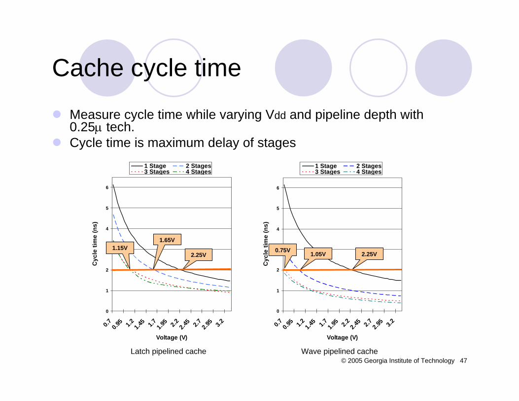
Modify CACTI* to measure cycle time of pipelined cache with variable Vdd

Latch pipelined cacheDivide CACTI cache model into four segmentsMerge adjacent segments to form 2-, 3- and 4-stage pipelined cache

Wave pipelined cacheCycle time using wave variable in CACTI

Decoder

Tag array &sense amp Comparator

Output driver

Pipeline segmentation for latch pipelined cache

CACTI cache structure

*Reinman, G. and Jouppi, N., CACTI 2.0: An integrated cache timing and power model. [Online]. Available http://www.research.compaq.com/wrl/people/jouppi/CACTI.html

Data array & sense amp

© 2005 Georgia Institute of Technology 47

Cache cycle time

Measure cycle time while varying Vdd and pipeline depth with 0.25µ tech.Cycle time is maximum delay of stages

0

1

2

3

4

5

6

0.7 0.95 1.2 1.45 1.7 1.95 2.2 2.45 2.7 2.95 3.2

Voltage (V)

Cyc

le ti

me

(ns)

1 Stage 2 Stages3 Stages 4 Stages

0

1

2

3

4

5

6

0.7 0.95 1.2 1.45 1.7 1.95 2.2 2.45 2.7 2.95 3.2

Voltage (V)

Cyc

le ti

me

(ns)

1 Stage 2 Stages3 Stages 4 Stages

Latch pipelined cache Wave pipelined cache

2.25V

1.65V1.15V

2.25V1.05V0.75V

© 2005 Georgia Institute of Technology 48

Experimental SetupEvaluate targeting embedded processor Simplescalar/ARM+Wattch* for performance and power estimation Modify Simplescalar/ARM+Wattchto simulate a variable stage pipelined cache processorMichigan ARM-like Verilog processor model (MARS**) for the power estimation of buffers between broken (non-cache) pipeline stagesExpand MARS pipeline and measure power consumption using synthesis based power measurement method

Binary Translation (GCC)

MARSVerilog Model

Functional Simulation

(VCS)

Benchmark Program (C/C++)

Toggle Rate Generation

Datapath Power(Power Compiler)

Synthesize Verilog Model

(Design Compiler)

Simplescalar/ARM+Wattch

Processor Power

CACTI Delay

Processor Energy

* D. Brooks et al., “Wattch: A Framework for Architectural Level Power Analysis and Optimizations,”Proceedings of the International Symposium on Computer Architecture, pp. 83-94, June 2000.

**The Simplescalar-Arm power modeling project. [Online]. Available http://www.eecs.umich.edu/~jringenb/power

© 2005 Georgia Institute of Technology 49

Architecture configuration and benchmarks

Simplescalar/ARM+Wattchconfiguration is modeled after Intel StrongARMBranch target buffer used to hide branch delay Compiler optimization used to hide load delay7 benchmarks targeting embedded system domain

2.25VVdd (Core)

2.25V, 1.05V0.75V

Vdd (Cache)

233MhzClock speed

12 cyclesMemory latency

4-byteMemory bus width

NoneL2 cache

32KB 4-wayL1 D-cache

32KB 4-wayL1 I-cache

128 entry BTBBranch predictor

In-orderExecution type

© 2005 Georgia Institute of Technology 50

Execution cycles

1-stage cache

Total Icache Dcache Total Icache Dcache Total Icache DcacheDIJKSTRA 100,437,638 109,881,681 9.40 1.13 8.27 127,199,801 26.65 2.38 24.26 141,488,147 30.11 5.11 25.00

DJPEG 10,734,606 11,380,700 6.02 0.34 5.68 12,243,399 14.06 0.74 13.32 13,091,913 15.41 1.84 13.57GSM 21,522,735 21,859,916 1.57 0.46 1.11 23,078,322 7.23 1.03 6.19 24,173,369 11.08 1.59 9.49

MPEG2DEC 28,461,724 29,398,489 3.29 0.28 3.01 31,741,379 11.52 1.27 10.25 33,969,889 15.87 2.37 13.50QSORT 90,206,190 93,280,904 3.41 1.91 1.50 97,111,275 7.65 4.10 3.55 100,787,822 10.08 6.74 3.34

SHA 17,533,248 17,600,241 0.38 0.34 0.04 18,014,403 2.74 0.74 2.00 18,413,569 4.98 1.14 3.84STRINGSEARCH 6,356,925 6,668,413 4.90 2.13 2.77 7,048,747 10.88 4.58 6.31 7,409,552 13.40 6.94 6.46

Average 4.14 0.94 3.20 11.53 2.12 9.41 14.42 3.68 10.74

Increase (%)cyclescycles

Increase (%)2-stage pipelined cache 3-stage pipelined cache 4-stage pipelined cache

Increase (%)cyclescyclesBenchmark

E.T. increases as the pipelined cache deepens due to pipelining penalties (branch misprediction, load delay)2-stage pipelined cache increases execution time by 4.14%

© 2005 Georgia Institute of Technology 51

Normalized processor power consumption

0.0

0.1

0.2

0.3

0.4

0.5

0.6

0.7

0.8

0.9

1.0

DIJKS

TRA

DJPEG

GSM

MPEG

2DEC

QSORT

SHA

STRIN

GSEARCH

1-stage 2-stage 3-stage 4-stage

2-stage pipelined cache processor saves 23.55% of power

Saving

© 2005 Georgia Institute of Technology 52

Normalized cache power consumption

0.0

0.1

0.2

0.3

0.4

0.5

0.6

0.7

0.8

0.9

1.0

DIJKS

TRA

DJPEG

GSM

MPEG

2DEC

QSORT

SHA

STRIN

GSEARCH

1-stage 2-stage 3-stage 4-stage

2-stage pipelined caches save about 70% of cache power

Saving

© 2005 Georgia Institute of Technology 53

Normalized energy consumption

0.0

0.1

0.2

0.3

0.4

0.5

0.6

0.7

0.8

0.9

1.0

DIJKSTR

A

DJPEG

GSM

MPEG

2DEC

QSORT

SHA

STRIN

GSEARCH

1-stage 2-stage 3-stage 4-stage

2-stage pipelined cache processor saves 20.43% of energy

Saving

© 2005 Georgia Institute of Technology 54

Outline

IntroductionRelated WorkSleepy stack Sleepy stack logic circuitsSleepy stack SRAMLow-power pipelined cache (LPPC)Sleepy stack pipelined SRAMConclusion

© 2005 Georgia Institute of Technology 55

Sleepy stack pipelined SRAMCombine the sleepy technique and low-power pipelined cache (LPPC)Leakage reduction while maintaining performanceUse 2-stage LPPC, i.e., 7-stage pipeline

IF1 IF2 ID EX MEM1 MEM2 WB

I-cache1 I-cache2 D-cache1 D-cache2

Sleepy stack low-power pipelined caches

Sleepy stack SRAM

© 2005 Georgia Institute of Technology 56

Methodology

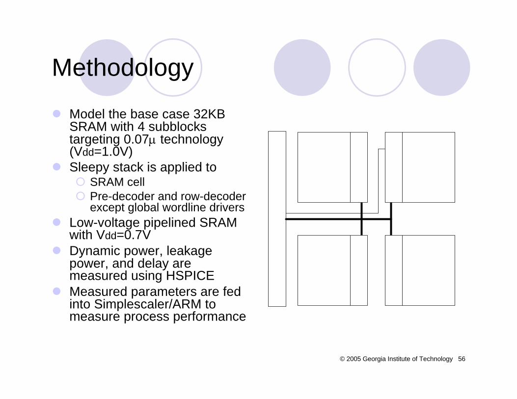
Model the base case 32KB SRAM with 4 subblocks targeting 0.07µ technology (Vdd=1.0V)Sleepy stack is applied to

SRAM cellPre-decoder and row-decoder except global wordline drivers

Low-voltage pipelined SRAM with Vdd=0.7VDynamic power, leakage power, and delay are measured using HSPICEMeasured parameters are fed into Simplescaler/ARM to measure process performance

© 2005 Georgia Institute of Technology 57

SRAM performance

0.00E+00

1.00E-02

2.00E-02

3.00E-02

4.00E-02

5.00E-02

6.00E-02

7.00E-02

8.00E-02

Basecase Low-voltageSRAM

Sleepystack SRAM

Active powerDecoder SRAM

0.00E+00

1.00E-03

2.00E-03

3.00E-03

4.00E-03

5.00E-03

6.00E-03

Basecase Low-voltageSRAM

Sleepystack SRAM

Static power

Decoder SRAM

Active power increases 36% (sleepy stack) and decreases 58% (low-voltage SRAM)Sleepy stack SRAM achieves 17X leakage reduction (low-voltage SRAM 3X)Delay increases 33% (low-voltage SRAM 66%) (before pipelining) Estimated area overhead of sleepy stack is less that 2X

0.00E+00

2.00E-10

4.00E-10

6.00E-10

8.00E-10

1.00E-09

1.20E-09

1.40E-09

1.60E-09

1.80E-09

Basecase Low-voltageSRAM

Sleepystack SRAM

Delay

Decoder SRAM subblock Rise/fall time

© 2005 Georgia Institute of Technology 58

Processor performance

Average 4% execution cycle increase with same cycle time (33% of delay increase before pipelining)Active power of sleepy stack pipelined SRAM increase 31% (low-voltage SRAM active power decreases 60%)When sleep mode is 3 times longer than active mode, the sleepy stack pipelined cache is effective to save energy

0

0.2

0.4

0.6

0.8

1

1.2

CJPEG

DIJKSTRA

DJPEG

GSM_ENCQSORT

MPEG2DEC1SHA

STRINGSEARCH

Averag

e

Normalized execution cycles

Base caseSleepy stack

0.00E+00

1.00E-02

2.00E-02

3.00E-02

4.00E-02

5.00E-02

6.00E-02

7.00E-02

Basecase Low-voltageSRAM

Sleepystack SRAM

Active powerI-cache D-cache

© 2005 Georgia Institute of Technology 59

Conclusion and contribution

Sleepy stack structure achieves dramatic leakage power reduction (4-inverters, 215X over forced stack) while saving state with some delay and area overheadSleepy stack SRAM cell provides new pareto points in ultra-low leakage power consumption (2.77X over high-Vth with 19% delay increase or 2.26X without delay increase)Low-power pipelined cache reduces cache power by lowering cache supply voltage (2-stage pipelined cache 20% of energy with 4% delay increase)Sleepy stack pipelined SRAM achieves 17X leakage reduction with small execution cycle (4%) increase and less than 2X estimate area increase

© 2005 Georgia Institute of Technology 60

Publications[1] J. C. Park, V. J. Mooney and P. Pfeiffenberger, “Sleepy Stack Reduction in Leakage

Power,” Proceedings of the International Workshop on Power and Timing Modeling, Optimization and Simulation (PATMOS’04), pp. 148-158, September 2004.

[2] P. Pfeiffenberger, J. C. Park and V. J. Mooney, “Some Layouts Using the Sleepy Stack Approach,” Technical Report GIT-CC-04-05, Georgia Institute of Technology, June 2004, [Online] Available http://www.cc.gatech.edu/tech_reports/index.04.html.

[3] A. Balasundaram, A. Pereira, J. C. Park and V. J. Mooney, “Golay and Wavelet Error Control Codes in VLSI,” Proceedings of the Asia and South Pacific Design Automation Conference (ASPDAC'04), pp. 563-564, January 2004.

[4] A. Balasundaram, A. Pereira, J. C. Park and V. J. Mooney, “Golay and Wavelet Error Control Codes in VLSI,” Technical Report GIT-CC-03-33, Georgia Institute of Technology, December 2003, [Online] Available http://www.cc.gatech.edu/tech_reports/index.03.html

[5] J. C. Park, V. J. Mooney and S. K. Srinivasan, “Combining Data Remapping and Voltage/Frequency Scaling of Second Level Memory for Energy Reduction in Embedded Systems,” Microelectronics Journal, 34(11), pp. 1019-1024, November 2003. Kluwer Academic/Plenum Publishers, pp. 211-224, May 2002.

© 2005 Georgia Institute of Technology 61

Publications[6] J. C. Park, V. J. Mooney, K. Palem and K. W. Choi, “Energy Minimization of a

Pipelined Processor using a Low Voltage Pipelined Cache,” Conference Record of the 36th Asilomar Conference on Signals, Systems and Computers (ASILOMAR'02), pp. 67-73, November 2002.

[7] K. Puttaswamy, K. W. Choi, J. C. Park, V. J. Mooney, A. Chatterjee and P. Ellervee, “System Level Power-Performance Trade-Offs in Embedded Systems Using Voltage and Frequency Scaling of Off-Chip Buses and Memory,” Proceedings of the International Symposium on System Synthesis (ISSS'02), pp. 225-230, October 2002.

[8] S. K. Srinivasan, J. C. Park and V. J. Mooney, “Combining Data Remapping and Voltage/Frequency Scaling of Second Level Memory for Energy Reduction in Embedded Systems,” Proceedings of the International Workshop on Embedded System Codesign (ESCODES'02), pp. 57-62, September 2002.

[9] K. Puttaswamy, L. N. Chakrapani, K. W. Choi, Y. S. Dhillon, U. Diril, P. Korkmaz, K. K. Lee, J. C. Park, A. Chatterjee, P. Ellervee, V. J. Mooney, K. Palem and W. F. Wong, “Power-Performance Trade-Offs in Second Level Memory Used by an ARM-Like RISC Architecture,” in the book Power Aware Computing, edited by Rami Melhem, University of Pittsburgh, PA, USA and Robert Graybill, DARPA/ITO, Arlington, VA, USA, published by Kluwer Academic/Plenum Publishers, pp. 211-224, May 2002.

[10] J. C. Park and V. J. Mooney, “Pareto Points in SRAM Design Using the Sleepy Stack Approach,” IFIP International Conference on Very Large Scale Integration (IFIP VLSI-SOC'05), 2005.


Recommended