Small Angle X Small Angle X - - ray Scattering Metrology for ray Scattering Metrology for Sidewall Angle and Cross Section of Nanometer Sidewall Angle and Cross Section of Nanometer Scale Line Gratings Scale Line Gratings Wen-Li Wu Ronald L. Jones, Tengjiao Hu, Christopher L. Soles, Eric K. Lin, Funding •NIST Office of Microelectronics Programs [email protected]ULSI, Richardson, TX March 18, 2005
Transcript
Small Angle XSmall Angle X--ray Scattering Metrology for ray Scattering Metrology for Sidewall Angle and Cross Section of Nanometer Sidewall Angle and Cross Section of Nanometer
Scale Line GratingsScale Line Gratings
Wen-Li Wu
Ronald L. Jones, Tengjiao Hu, Christopher L. Soles, Eric K. Lin,
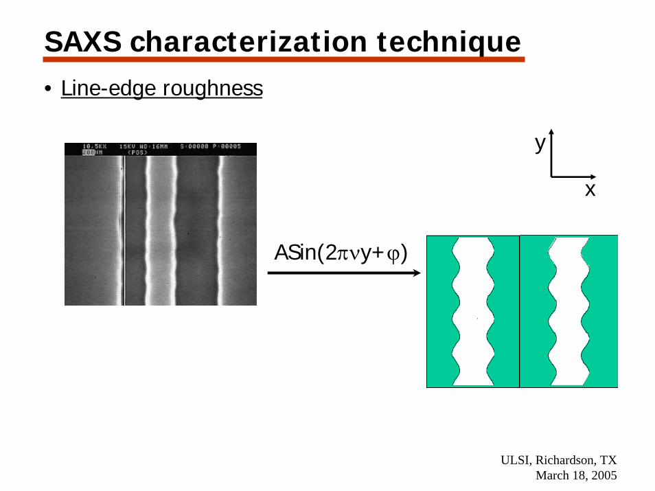
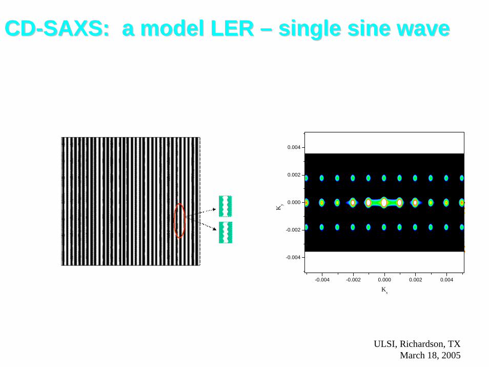
•Line roughness including both side walls & top surface (on-going)
•Conclusions
ULSI, Richardson, TXMarch 18, 2005
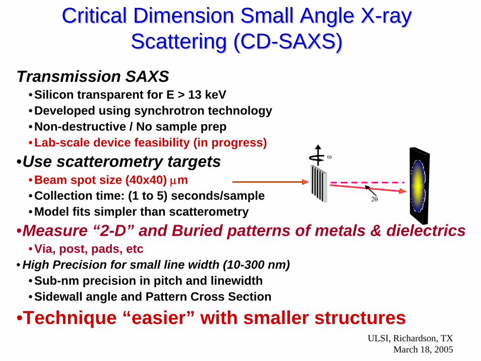
Critical Dimension Small Angle XCritical Dimension Small Angle X--ray ray Scattering (CDScattering (CD--SAXS)SAXS)
ω
2θ
Transmission SAXS•Silicon transparent for E > 13 keV•Developed using synchrotron technology•Non-destructive / No sample prep•Lab-scale device feasibility (in progress)
•Use scatterometry targets•Beam spot size (40x40) µm•Collection time: (1 to 5) seconds/sample•Model fits simpler than scatterometry
•Measure “2-D” and Buried patterns of metals & dielectrics•Via, post, pads, etc
• High Precision for small line width (10-300 nm)•Sub-nm precision in pitch and linewidth•Sidewall angle and Pattern Cross Section
•Technique “easier” with smaller structuresULSI, Richardson, TX
March 18, 2005
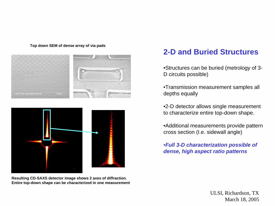
Top down SEM of dense array of via pads
2-D and Buried Structures
•Structures can be buried (metrology of 3-D circuits possible)
•Transmission measurement samples all depths equally
•2-D detector allows single measurement to characterize entire top-down shape.
•Additional measurements provide pattern cross section (I.e. sidewall angle)
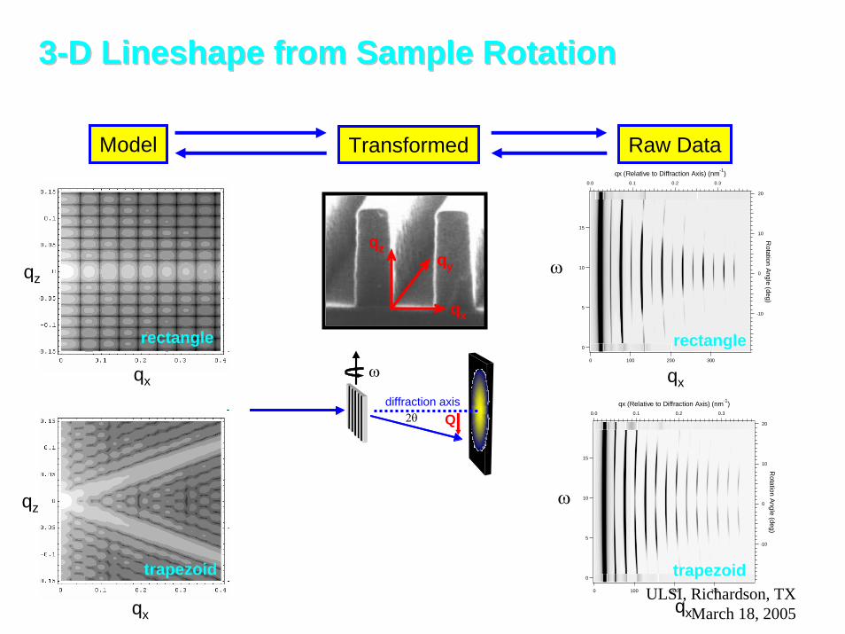
•Full 3-D characterization possible of dense, high aspect ratio patterns
Resulting CD-SAXS detector image shows 2 axes of diffraction. Entire top-down shape can be characterized in one measurement
ULSI, Richardson, TXMarch 18, 2005
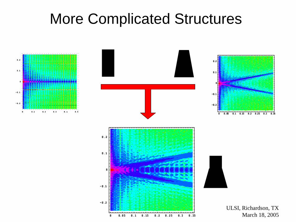
A Wide Range of SamplesA Wide Range of SamplesDense (1:1 spacing) 550 nm lines
Pattern GeometriesPattern Geometries••Line/Space patterns (gratings)Line/Space patterns (gratings)••Arrays of columnsArrays of columns••Arrays of holes (Arrays of holes (viasvias))
ULSI, Richardson, TXMarch 18, 2005
Hexagonal Close Packed 60 nm vias
Line/Space Patterns in Oxide
Sparse (1:10 spacing) 15nm lines
6
7
8
91000
2
3
Inte
nsity
0.350.300.250.200.150.100.050.00
qx (nm-1)
Model Name: Rectangle Period (nm): 173 Line Width (nm): 15 Line Height (nm): 370 Dev. in Period (nm): 4 Pattern SLD (cm^-2): 1e+10 Scale Factor: 6 Background: 600
FILE: ISMT_S103_R_046.dat
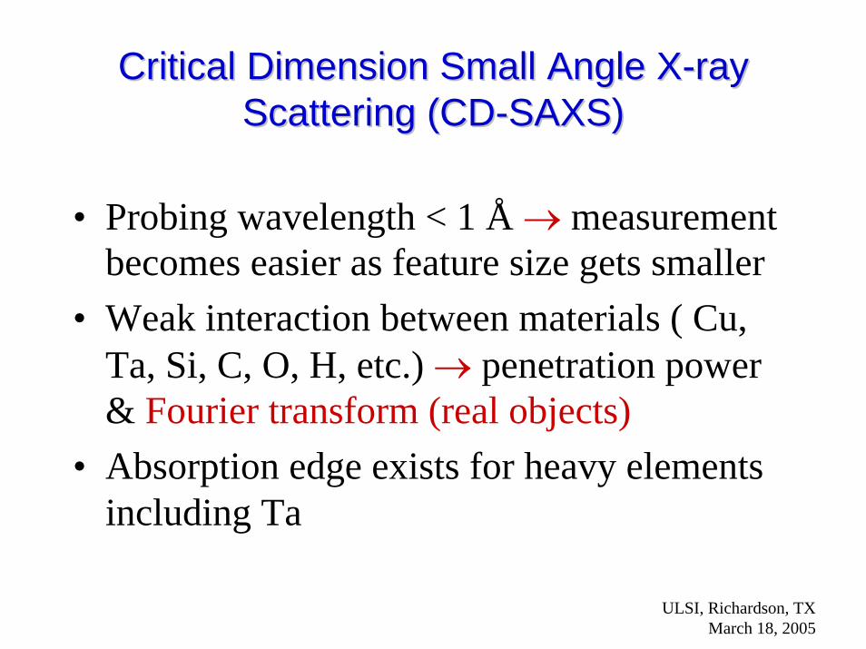
Critical Dimension Small Angle XCritical Dimension Small Angle X--ray ray Scattering (CDScattering (CD--SAXS)SAXS)
• Probing wavelength < 1 Å → measurement becomes easier as feature size gets smaller
• Weak interaction between materials ( Cu, Ta, Si, C, O, H, etc.) → penetration power & Fourier transform (real objects)
• Absorption edge exists for heavy elements including Ta
ULSI, Richardson, TXMarch 18, 2005
challenges
• Quantify imperfections of nano-pattern from X-ray data
• Availability of intense x-ray source other than synchrotron
ULSI, Richardson, TXMarch 18, 2005
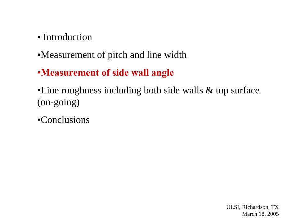
• Introduction
•Measurement of pitch and line width
•Measurement of side wall angle and height
•Line roughness including both side walls & top surface (on-going)
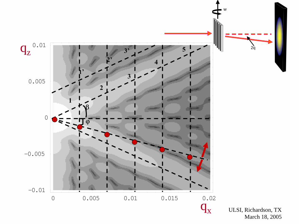
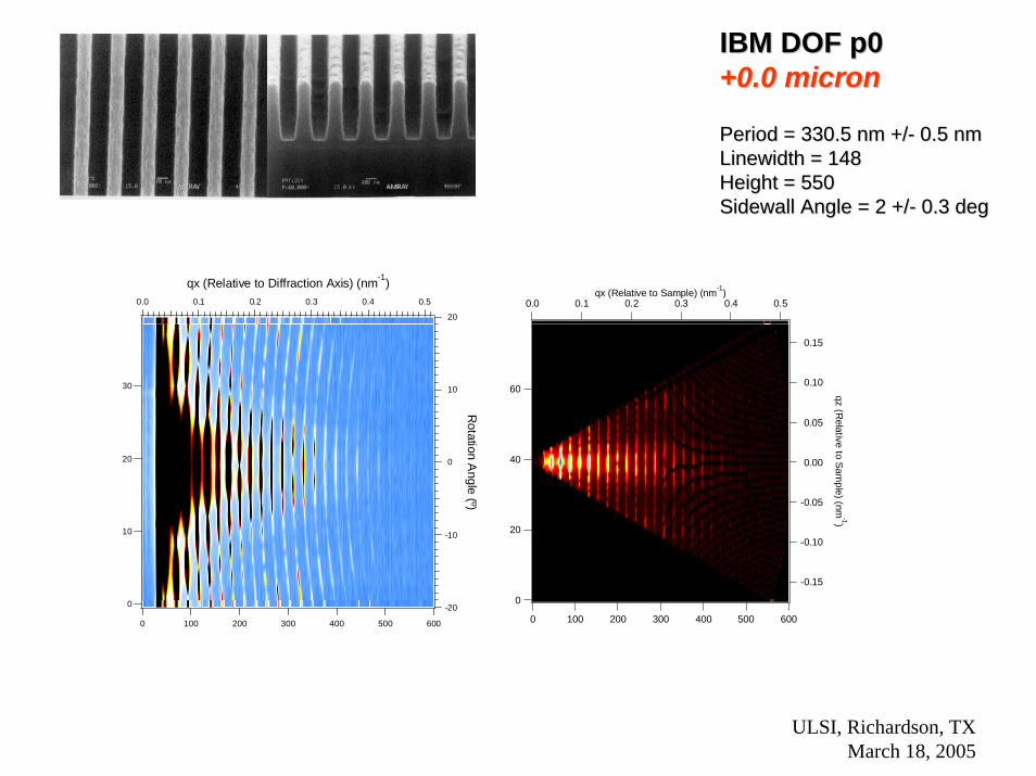
2. Line width – intensity modulation along qx at qz =0
3. Line height – periodicity along qz at a fixed qx
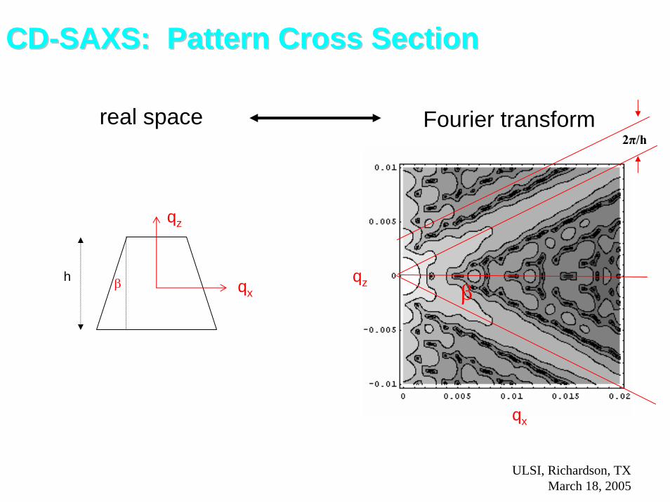
4. Sidewall angle
ULSI, Richardson, TXMarch 18, 2005
Photoresist Patterns Photoresist Patterns
Data measured on 5Data measured on 5--ID SAXS (DNDID SAXS (DND--CAT)CAT)Advanced Photon Source, Argonne National LabAdvanced Photon Source, Argonne National Lab
Data collection and analysis performed byData collection and analysis performed byRon Jones, Tengjiao Hu, WenRon Jones, Tengjiao Hu, Wen--li Wuli WuBeamline Scientists: Steve Weigand, John QuintanaBeamline Scientists: Steve Weigand, John QuintanaSamples: provided by Samples: provided by QinghuanQinghuan Lin (IBM T.J. Watson Research)Lin (IBM T.J. Watson Research)
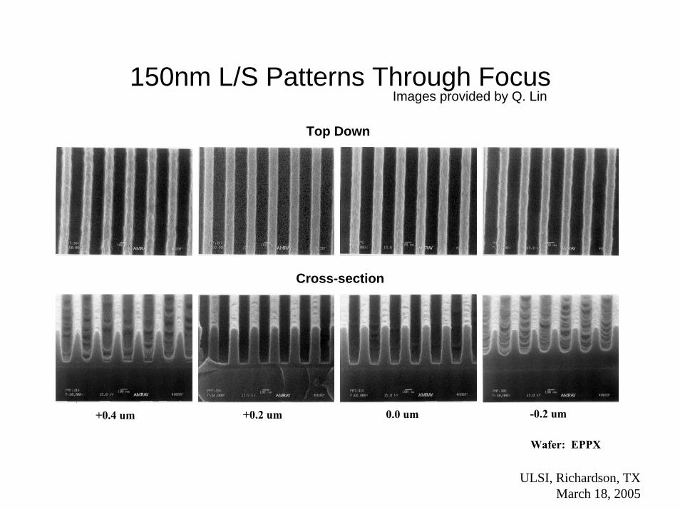
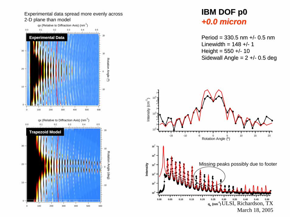
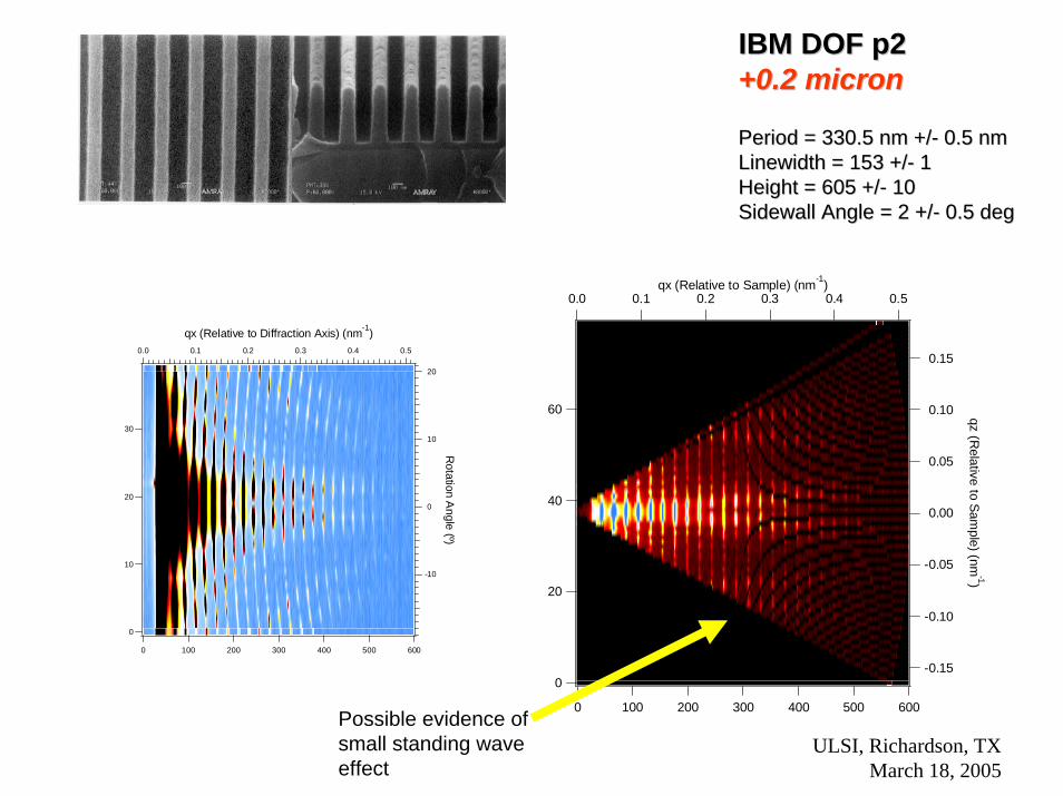
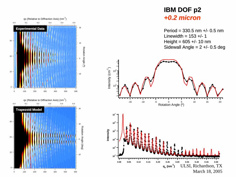
Sample List:Sample List:1) IBM DOF m2 1) IBM DOF m2 -- 248nm PR, 248nm PR, --0.2micron Depth of Focus0.2micron Depth of Focus2) IBM DOF p0 2) IBM DOF p0 -- 248nm PR, “Optimal” Depth of Focus248nm PR, “Optimal” Depth of Focus3) IBM DOF p2 3) IBM DOF p2 -- 248nm PR, +0.2micron Depth of Focus248nm PR, +0.2micron Depth of Focus4) IBM DOF p4 4) IBM DOF p4 -- 248nm PR, +0.4micron Depth of Focus248nm PR, +0.4micron Depth of Focus
ULSI, Richardson, TXMarch 18, 2005
150nm L/S Patterns Through FocusImages provided by Q. Lin
Intensity integrated +/- 45 deg normal to diffraction axis
ULSI, Richardson, TXMarch 18, 2005
CDCD--SAXS: Measuring CD and PitchSAXS: Measuring CD and Pitch
1.E+00
1.E+01
1.E+02
1.E+03
1.E+04
1.E+05
1.E+06
1.E+07
0 0.01 0.02
q (A-1)
Inte
nsity
(cm
-1)
q
Basic Model:
•Simple Rectangular Profile
•Pitch determined from period of diffraction peaks
•Line width determined from relative intensities
•Decay of intensities fit with Debye-Waller factor
•Peak profiles fit with Voigt function
Data fitting performed rapidly due to simplicity of modeling anddata analysis procedures (I.e. no libraries of solutions required)
ULSI, Richardson, TXMarch 18, 2005
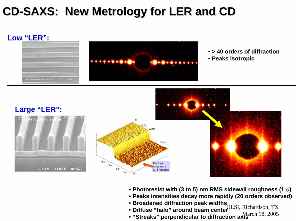
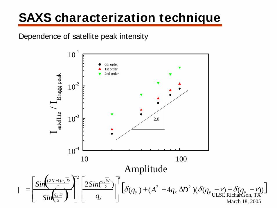
Observable defects in SAXS patterns
Fourier space Real space
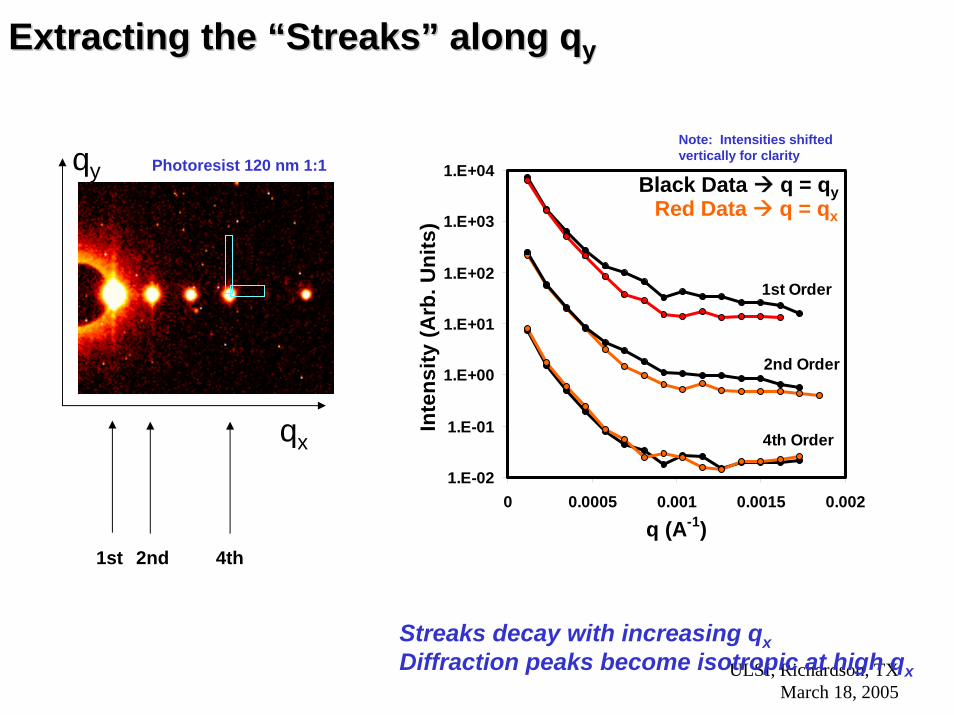
•Strikes along qy direction
•Amorphous halo
•Debye-Waller factor
•Side wall & top surface roughness
•Mass fluctuations along each line
•Position fluctuation of the center of each lines
ULSI, Richardson, TXMarch 18, 2005
ConclusionsConclusions
• Methodology for pitch, line width, side wall angle is in place, detail cross sectional modeling is within reach
• Methodology for line surface roughness, linear mass fluctuation and center position fluctuation is in research stage
ULSI, Richardson, TXMarch 18, 2005
Conclusions (cont.)
•The wavelength of the probing x-ray beam can be calibrated with great precision; there is no need to calibrate the resulting dimensions from x-ray measurements
•A potential laboratory based metrology complementary to SEM, AFM and optical scattometry
ULSI, Richardson, TXMarch 18, 2005
AcknowledgementsAcknowledgements
•X-ray measurements were conducted at Advanced Photon Source of Argonne National Laboratory


![Angle metrology at INRIM in the framework of the EMRP ... · experience made at INRIM with the previous nano angle generator described in [7]. In that device we found out that the](https://static.documents.pub/doc/80x56/5ec72275f4da254080258a8b/angle-metrology-at-inrim-in-the-framework-of-the-emrp-experience-made-at-inrim.jpg)


