Analog Input Monaural Class-D Speaker Amplifiers BD5632NUX,BD5634NUX,BD5638NUX
Description
BD5632NUX, BD5634NUX and BD5638NUX are a low voltage drive class-D speaker amplifier that was developed for mobile phones, mobile audio products and the others. BD5632NUX has a fixed gain of 6dB, BD5634NUX has a fixed gain of 12dB, and BD5638NUX has a fixed gain of 18dB. It is suitable for the application of battery drive because of high efficiency and low power consumption. Also, stand-by current is 0µA (typ.), and fast transitions from standby to active with little pop noise. It is suitable for applications that switch repeatedly between stand-by and active.
Features
1) LC Filter less 2) Only 3 external components 3) High power 2.5W/4ohm/BTL (VDD=5V, RL=4ohm, THD+N=10%, typ.) 4) High power 0.85W/8ohm/BTL (VDD=3.6V, RL=8ohm, THD+N=10%, typ.) 5) Analog differential input / PWM digital output 6) Pop noise suppression circuit 7) Standby function (Mute function) 8) Protection circuit (Short protection [Auto recover without power cycling], Thermal shutdown, under voltage lockout) 9) Ultra small package VSON008X2030 (2.0×3.0×0.6mmMAX)
Applications
Mobile phones, PND (Personal Navigation Device), DSC, PDA, etc Line up matrix
Production Name BD5632NUX BD5634NUX BD5638NUX
Gain (dB) 6 12 18
Input Impedance (kΩ) 100 50 25
Package VSON008X2030
Absolute maximum ratings (Ta=25)
Parameter Symbol Ratings Unit
Power Supply Voltage VDD 7.0 V
Power Dissipation Pd 0.52 *1 W
Storage Temperature Range Tstg -55 ~ +150
STBY Terminal Input Range Vstby -0.3 ~ VDD+0.3 V
IN+, IN- Terminal Input Range Vin -0.3 ~ VDD+0.3 V (*1) ROHM standard board mounted (Board size 70mm×70mm×1.6mmt, 1layer), de-rate the value 4.16mW/deg above Ta=+25deg.
Operating conditions
Parameter Symbol Ratings Unit
Power Supply Voltage VDD +2.5 ~ +5.5 V
Temperature Range Topr -40 ~ +85 *This product is not designed for protection against radioactive rays.
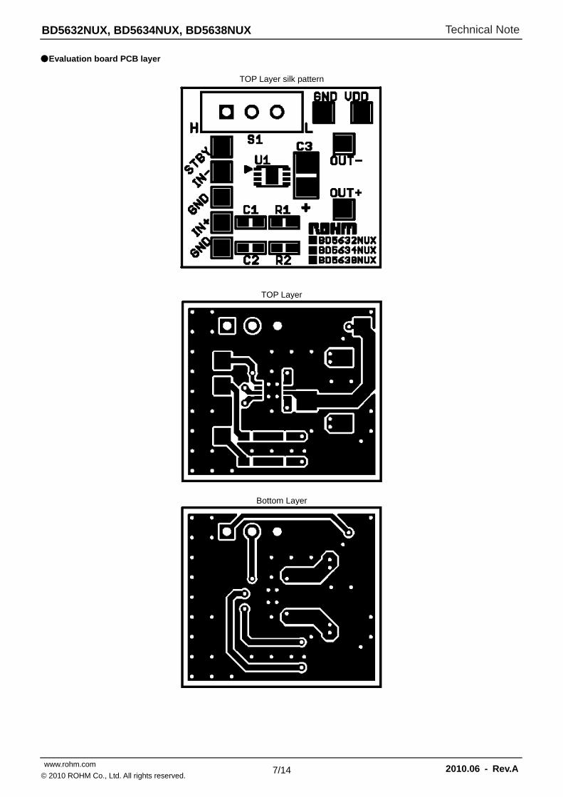
1. Input coupling capacitor (C1, C2) It makes an Input coupling capacitor 0.47µF. It sets cutoff frequency fc by the following formula by input coupling capacitor C1 (=C2) and input impedance Ri. In case of C1 (=C2) =0.47µF BD5632NUX Ri =100kΩ : fc=3.5Hz BD5634NUX Ri =50kΩ : fc=7Hz BD5638NUX Ri =25kΩ : fc=14Hz
2. Power decoupling capacitor (C3)
It makes a power decoupling capacitor 10µF. When making capacitance of the power decoupling capacitor, there is an influence in the Audio characteristic. When making small, careful for the Audio characteristic at the actual application.
When measuring Audio characteristics, insert LC filter during the output terminal of IC and the speaker load and measure it. Arrange LC filter as close as possible to the output terminal of IC. In case of L=22µH, C=1µF, the cut-off frequency becomes the following.
About the thermal design by the IC Characteristics of an IC have a great deal to do with the temperature at which it is used, and exceeding absolute maximum ratings may degrade and destroy elements. Careful consideration must be given to the heat of the IC from the two standpoints of immediate damage and long-term reliability of operation. Pay attention to points such as the following. Since a maximum junction temperature (TjMAX.)or operating temperature range (Topr) is shown in the absolute maximum ratings of the IC, to reference the value, find it using the Pd-Ta characteristic (temperature derating curve). If an input signal is too great when there is insufficient radiation, TSD (thermal shutdown) may operate. TSD, which operates at a chip temperature of approximately +180deg, is canceled when this goes below approximately +100deg. Since TSD operates persistently with the purpose of preventing chip damage, be aware that long-term use in the vicinity that TSD affects decrease IC reliability.
Temperature Derating Curve
Power dissipation values vary according to the board on which the IC is mounted. The Power dissipation of this IC when mounted on a multilayer board designed to radiate is greater than the values in the graph above.
Reference Data
VSON008X20301.0
0.5
0.0
0 25 50 75 100 125 150
Ambient Temperature Ta (deg)
Pow
er D
issi
patio
n P
d(W)
0.52W
Measurement conditions: IC unit and Rohm standard board mount board size : 70mm×70mm x 1.6mm 1layer
θja = 240.4 deg/W
85
Note) Values are actual measurements and are not guaranteed.
Notes for use (1) Numbers and data in entries are representative design values and are not guaranteed values of the items. (2) Although we are confident recommending the sample application circuit, carefully check their characteristics further when
using them. When modifying externally attached component constants before use, determine them so that they have sufficient margins by taking into account variations in externally attached components and the Rohm IC, not only for static characteristics but also including transient characteristics.
(3) Absolute maximum ratings
This IC may be damaged if the absolute maximum ratings for the applied voltage, temperature range, or other parameters are exceeded. Therefore, avoid using a voltage or temperature that exceeds the absolute maximum ratings. If it is possible that absolute maximum ratings will be exceeded, use fuses or other physical safety measures and determine ways to avoid exceeding the IC's absolute maximum ratings.
(4) GND terminal’s potential
Try to set the minimum voltage for GND terminal’s potential, regardless of the operation mode. (5) Shorting between pins and mounting errors
When mounting the IC chip on a board, be very careful to set the chip's orientation and position precisely. When the power is turned on, the IC may be damaged if it is not mounted correctly. The IC may also be damaged if a short occurs (due to a foreign object, etc.) between two pins, between a pin and the power supply, or between a pin and the GND.
(6) Operation in strong magnetic fields
Note with caution that operation faults may occur when this IC operates in a strong magnetic field. (7) Thermal design
Ensure sufficient margins to the thermal design by taking in to account the allowable power dissipation during actual use modes, because this IC is power amp. When excessive signal inputs which the heat dissipation is insufficient condition, it is possible that thermal shutdown circuit is active.
(8) Thermal shutdown circuit
This product is provided with a built-in thermal shutdown circuit. When the thermal shutdown circuit operates, the output transistors are placed under open status. The thermal shutdown circuit is primarily intended to shut down the IC avoiding thermal runaway under abnormal conditions with a chip temperature exceeding Tjmax = +150deg, and is not intended to protect and secure an electrical appliance.
(9) Load of the output terminal
This IC corresponds to dynamic speaker load, and doesn't correspond to the load except for dynamic speakers.
(10) The short protection of the output terminal The short-circuiting protection of this IC corresponds only to “VDD-short” (the short-circuiting with the power) of the output terminal and “GND-short” (the short-circuiting with GND) of the output terminal. It doesn't correspond to the short-circuiting among the output terminals. Also, when the short-circuiting condition of the output terminal is canceled, it detects the high impedance of the output terminal and it is equipped with the auto recover without power cycling(the cancellation) function in the short-circuiting protection. Be careful of the output terminal, because, there is a fear not to return automatically when the short-circuiting condition occurs in pull-up or the pull-down at equal to or less than about 1MΩ impedance.
(11) Operating ranges
The rated operating power supply voltage range (VDD=+2.5V ~ +5.5V) and the rated operating temperature range (Ta=-40deg ~ +85deg) are the range by which basic circuit functions is operated. Characteristics and rated output power are not guaranteed in all power supply voltage ranges or temperature ranges.
(12) Electrical characteristics
Electrical characteristics show the typical performance of device and depend on board layout, parts, power supply. The standard value is in mounting device and parts on surface of ROHM’s board directly.
(13) Power decoupling capacitor
Because the big peak current flows through the power line, the class-D amplifier has an influence on the Audio characteristic by the capacitance value or the arrangement part of the power decoupling capacitor. Arrange a power decoupling capacitor as close as possible to the VDD terminal of IC.
(14) NC terminal (Pin2)
NC terminal (Non Connection Pin) does not connect to the inside circuit. Therefore, please open or connect to GND.
1. Our Products are designed and manufactured for application in ordinary electronic equipments (such as AV equipment, OA equipment, telecommunication equipment, home electronic appliances, amusement equipment, etc.). If you intend to use our Products in devices requiring extremely high reliability (such as medical equipment (Note 1), transport equipment, traffic equipment, aircraft/spacecraft, nuclear power controllers, fuel controllers, car equipment including car accessories, safety devices, etc.) and whose malfunction or failure may cause loss of human life, bodily injury or serious damage to property (“Specific Applications”), please consult with the ROHM sales representative in advance. Unless otherwise agreed in writing by ROHM in advance, ROHM shall not be in any way responsible or liable for any damages, expenses or losses incurred by you or third parties arising from the use of any ROHM’s Products for Specific Applications.
(Note1) Medical Equipment Classification of the Specific Applications JAPAN USA EU CHINA
CLASSⅢ CLASSⅢ
CLASSⅡb CLASSⅢ
CLASSⅣ CLASSⅢ
2. ROHM designs and manufactures its Products subject to strict quality control system. However, semiconductor
products can fail or malfunction at a certain rate. Please be sure to implement, at your own responsibilities, adequate safety measures including but not limited to fail-safe design against the physical injury, damage to any property, which a failure or malfunction of our Products may cause. The following are examples of safety measures:
[a] Installation of protection circuits or other protective devices to improve system safety [b] Installation of redundant circuits to reduce the impact of single or multiple circuit failure
3. Our Products are designed and manufactured for use under standard conditions and not under any special or extraordinary environments or conditions, as exemplified below. Accordingly, ROHM shall not be in any way responsible or liable for any damages, expenses or losses arising from the use of any ROHM’s Products under any special or extraordinary environments or conditions. If you intend to use our Products under any special or extraordinary environments or conditions (as exemplified below), your independent verification and confirmation of product performance, reliability, etc, prior to use, must be necessary:
[a] Use of our Products in any types of liquid, including water, oils, chemicals, and organic solvents [b] Use of our Products outdoors or in places where the Products are exposed to direct sunlight or dust [c] Use of our Products in places where the Products are exposed to sea wind or corrosive gases, including Cl2,
H2S, NH3, SO2, and NO2
[d] Use of our Products in places where the Products are exposed to static electricity or electromagnetic waves [e] Use of our Products in proximity to heat-producing components, plastic cords, or other flammable items [f] Sealing or coating our Products with resin or other coating materials [g] Use of our Products without cleaning residue of flux (even if you use no-clean type fluxes, cleaning residue of
flux is recommended); or Washing our Products by using water or water-soluble cleaning agents for cleaning residue after soldering
[h] Use of the Products in places subject to dew condensation
4. The Products are not subject to radiation-proof design. 5. Please verify and confirm characteristics of the final or mounted products in using the Products. 6. In particular, if a transient load (a large amount of load applied in a short period of time, such as pulse. is applied,
confirmation of performance characteristics after on-board mounting is strongly recommended. Avoid applying power exceeding normal rated power; exceeding the power rating under steady-state loading condition may negatively affect product performance and reliability.
7. De-rate Power Dissipation (Pd) depending on Ambient temperature (Ta). When used in sealed area, confirm the actual
ambient temperature. 8. Confirm that operation temperature is within the specified range described in the product specification. 9. ROHM shall not be in any way responsible or liable for failure induced under deviant condition from what is defined in
this document.
Precaution for Mounting / Circuit board design 1. When a highly active halogenous (chlorine, bromine, etc.) flux is used, the residue of flux may negatively affect product
performance and reliability. 2. In principle, the reflow soldering method must be used; if flow soldering method is preferred, please consult with the
ROHM representative in advance. For details, please refer to ROHM Mounting specification
Precautions Regarding Application Examples and External Circuits 1. If change is made to the constant of an external circuit, please allow a sufficient margin considering variations of the
characteristics of the Products and external components, including transient characteristics, as well as static characteristics.
2. You agree that application notes, reference designs, and associated data and information contained in this document
are presented only as guidance for Products use. Therefore, in case you use such information, you are solely responsible for it and you must exercise your own independent verification and judgment in the use of such information contained in this document. ROHM shall not be in any way responsible or liable for any damages, expenses or losses incurred by you or third parties arising from the use of such information.
Precaution for Electrostatic
This Product is electrostatic sensitive product, which may be damaged due to electrostatic discharge. Please take proper caution in your manufacturing process and storage so that voltage exceeding the Products maximum rating will not be applied to Products. Please take special care under dry condition (e.g. Grounding of human body / equipment / solder iron, isolation from charged objects, setting of Ionizer, friction prevention and temperature / humidity control).
Precaution for Storage / Transportation 1. Product performance and soldered connections may deteriorate if the Products are stored in the places where:
[a] the Products are exposed to sea winds or corrosive gases, including Cl2, H2S, NH3, SO2, and NO2 [b] the temperature or humidity exceeds those recommended by ROHM [c] the Products are exposed to direct sunshine or condensation [d] the Products are exposed to high Electrostatic
2. Even under ROHM recommended storage condition, solderability of products out of recommended storage time period may be degraded. It is strongly recommended to confirm solderability before using Products of which storage time is exceeding the recommended storage time period.
3. Store / transport cartons in the correct direction, which is indicated on a carton with a symbol. Otherwise bent leads
may occur due to excessive stress applied when dropping of a carton. 4. Use Products within the specified time after opening a humidity barrier bag. Baking is required before using Products of
which storage time is exceeding the recommended storage time period.
Precaution for Product Label QR code printed on ROHM Products label is for ROHM’s internal use only.
Precaution for Disposition When disposing Products please dispose them properly using an authorized industry waste company.
Precaution for Foreign Exchange and Foreign Trade act Since our Products might fall under controlled goods prescribed by the applicable foreign exchange and foreign trade act, please consult with ROHM representative in case of export.
Precaution Regarding Intellectual Property Rights 1. All information and data including but not limited to application example contained in this document is for reference
only. ROHM does not warrant that foregoing information or data will not infringe any intellectual property rights or any other rights of any third party regarding such information or data. ROHM shall not be in any way responsible or liable for infringement of any intellectual property rights or other damages arising from use of such information or data.:
2. No license, expressly or implied, is granted hereby under any intellectual property rights or other rights of ROHM or any
third parties with respect to the information contained in this document.
Other Precaution 1. This document may not be reprinted or reproduced, in whole or in part, without prior written consent of ROHM. 2. The Products may not be disassembled, converted, modified, reproduced or otherwise changed without prior written
consent of ROHM. 3. In no event shall you use in any way whatsoever the Products and the related technical information contained in the
Products or this document for any military purposes, including but not limited to, the development of mass-destruction weapons.
4. The proper names of companies or products described in this document are trademarks or registered trademarks of
General Precaution 1. Before you use our Pro ducts, you are requested to care fully read this document and fully understand its contents.
ROHM shall n ot be in an y way responsible or liabl e for fa ilure, malfunction or acci dent arising from the use of a ny ROHM’s Products against warning, caution or note contained in this document.
2. All information contained in this docume nt is current as of the issuing date and subj ect to change without any prior
notice. Before purchasing or using ROHM’s Products, please confirm the la test information with a ROHM sale s representative.
3. The information contained in this doc ument is provi ded on an “as is” basis and ROHM does not warrant that all
information contained in this document is accurate an d/or error-free. ROHM shall not be in an y way responsible or liable for any damages, expenses or losses incurred by you or third parties resulting from inaccuracy or errors of or concerning such information.