Page 1
Worcester Polytechnic InstituteDigital WPI
Major Qualifying Projects (All Years) Major Qualifying Projects
April 2017
Smart Battery ChargerSeth O. GyebiWorcester Polytechnic Institute
Follow this and additional works at: https://digitalcommons.wpi.edu/mqp-all
This Unrestricted is brought to you for free and open access by the Major Qualifying Projects at Digital WPI. It has been accepted for inclusion inMajor Qualifying Projects (All Years) by an authorized administrator of Digital WPI. For more information, please contact [email protected] .
Repository CitationGyebi, S. O. (2017). Smart Battery Charger. Retrieved from https://digitalcommons.wpi.edu/mqp-all/2923
Page 2
1
Major Qualifying Project
Smart Battery Charger
Students: Seth Gyebi
Advisor: Professor Alexander E. Emanuel
Term: C/D 2017
Submitted to: Department of Electrical and Computer Engineering
Page 3
2
Smart Battery Charger
A Major Qualifying Project
Submitted to the Faculty of
WORCESTER POLYTECHNIC INSTITUTE
In partial fulfilment of the requirements for the Degree of Bachelor of Science
By Seth Gyebi
Date: 25 March 2017
Page 4
3
This report represents work of WPI undergraduate students submitted to the faculty as evidence
of a degree requirement. WPI routinely publishes these reports on its web site without editorial
or peer review. For more information about the projects program at WPI, see
http://www.wpi.edu/Academics/Projects
Page 5
4
ACKNOWLEDGEMENTS
I would like to thank my advisor Professor Alexander E. Emanuel for his continuing help and
expertise in developing and completing this project. I would also like to thank all the previous
MQP teams who have worked on similar projects for laying the groundwork for my own.
Page 6
5
ABSTRACT
The purpose of this project was to design, build and test a 1A smart battery charger that
accurately and efficiently charges a 3V, 6V or 12V battery. The smart battery charging system
integrated an AC/DC converter, a MOSFET driver circuit, and a DC/DC converter to charge the
battery. The concepts of experimental design and simulation were observed.
Page 7
6
Table of Contents
1 CHAPTER 1: Introduction 10
2 CHAPTER 2: Architectural Description 11
2.1 Project Overview 11
2.2 Modular Breakdown 12
2.2.1 Surge Protection 12
2.2.2 AC /DC Conversion (Rectifier) 13
2.2.3 DC/DC Conversion 13
3 CHAPTER 3: Module Description and Analysis 14
3.1 Transformer 15
3.2 AC/DC Converter 16
3.3 DC/DC Converter 17
3.3.1 Astable Multivibrator using LM741 OP-AMP 18
3.3.2 Comparator 20
3.3.3 BJT 22
3.3.4 MOSFET 23
3.3.5 Filter Inductor 23
4. CHAPTER 4: Module Simulation 25
4.1 Multisim Result 26
Page 8
7
4.2 PSpice Simulation 27
4.3 Pspice Result 28
5 CHAPTER 5: System Testing 33
5.1 AC/DC Module Testing 33
5.2 Driver Circuit Testing 35
5.3 Inductor Output Testing 36
5.4 Final battery charging verification 37
6 Conclusion 38
7 References 39
Appendix A 41
Page 9
8
TABLE OF FIGURES
Figure 1: Flow Chart. .................................................................................................................... 11
Figure 2: Surge protection. ........................................................................................................... 12
Figure 3: Functional Block Diagram. ........................................................................................... 14
Figure 4: AC/DC Converter Circuit. ............................................................................................. 16
Figure 5: DC/DC Converter Circuit. ............................................................................................. 17
Figure 6: Timer astable circuit. ..................................................................................................... 18
Figure 7: Timer astable multivibrator output square wave. .......................................................... 19
Figure 8: Timer astable multivibrator capacitor voltage. .............................................................. 20
Figure 9: Comparator. ................................................................................................................... 21
Figure 10: Comparator input and output waveform. Red is input, blue is control voltage and
green is output. .............................................................................................................................. 22
Figure 11: MOSFET and BJT ....................................................................................................... 23
Figure 12: Filter inductor output ................................................................................................... 24
Figure 13: Module simulations circuit .......................................................................................... 25
Figure 14: Rectifier DC waveform ............................................................................................... 26
Figure 15: Oscillator and Comparator .......................................................................................... 27
Figure 16: Pspice simulation circuit ............................................................................................. 28
Figure 17: Simulated waveform for the current inductor. ............................................................ 29
Figure 18: Simulated waveform for voltage of the inductor ......................................................... 29
Figure 19: Simulated waveform for the voltage of the diode, inductor and the load. .................. 30
Figure 20: Simulated waveform for the voltage of the load ......................................................... 31
Figure 21: Simulated waveform for the voltage of the MOSFET. ............................................... 31
Page 10
9
Figure 22: Simulated waveform for the voltage of the driver ...................................................... 32
Figure 23: Simulated waveform current between diode ............................................................... 32
Figure 24: Smart battery charger circuit. ...................................................................................... 33
Figure 25: AC/DC Module testing. ............................................................................................... 34
Figure 26 : Measured waveform for the output rectifier and the polarity legs of the rectifier. .... 34
Figure 27: Measured oscillator output. ......................................................................................... 35
Figure 28: Measured comparator output. ...................................................................................... 35
Figure 29: Inductor output testing. ................................................................................................ 36
Figure 30: Battery charger verification ......................................................................................... 37
Page 11
10
1 CHAPTER 1: Introduction
The purpose of this project was to introduce and provide a detailed description and
practical analysis of the project design approach to build a smart battery charger. The original
design for a smart charger consisted of a number of modules; an AC/DC conversion circuit, a
driver circuit and a filter circuit. A full bridge rectifier will be used to convert an AC source
(110/220V) to DC. A switch and a fuse were placed in series to prevent damage in the event of a
power spike. In addition to regulating the power output to charge the battery, the power source
supplies the astable multivibrator to power the driver to regulate the charging voltage.
Page 12
11
2 CHAPTER 2: Architectural Description
The figure below describes the basic architecture features of the smart battery charger.
The battery charger is made up of the following functional blocks:
2.1 Project Overview
Figure 1: Flow Chart.
Page 13
12
2.2 Modular Breakdown
2.2.1 Surge Protection
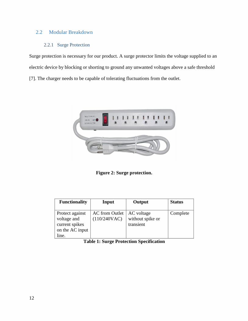
Surge protection is necessary for our product. A surge protector limits the voltage supplied to an
electric device by blocking or shorting to ground any unwanted voltages above a safe threshold
[7]. The charger needs to be capable of tolerating fluctuations from the outlet.
Figure 2: Surge protection.
Functionality Input Output Status
Protect against voltage and current spikes on the AC input line.
AC from Outlet (110/240VAC)
AC voltage without spike or transient
Complete
Table 1: Surge Protection Specification
Page 14
13
2.2.2 AC /DC Conversion (Rectifier)
The AC/DC rectifier converts 12V (RMS value) AC voltage at the transformer secondary side
into a DC voltage. Meanwhile, it must be able to support at least 1A of current for the battery
charging.
2.2.3 DC/DC Conversion
The DC/DC converter needs to filter out the rectifier’s DC voltage output ripple and convert it
into a clean, constant DC voltage output at the terminal of the battery. The converter must also
be able to regulate the DC output to the desired battery charging voltage of either 3V, 6V, or
12V.
Page 15
14
3 CHAPTER 3: Module Description and Analysis
The figure below describes the basic architecture features of the smart battery charger.
The battery charger is made up of the following functional blocks: an AC Input (circuit
protection, transformer), a full bridge rectifier, a diver, and a filter which consists of an inductor
and a load.
Figure 3: Functional Block Diagram.
The smart battery charger is supplied by 120Vrms/240Vrms, 50/60Hz AC from the wall. It is
protected by a MOV (metal-oxide varistor) switch in the wall outlet that conducts current to
Page 16
15
ground in cause of a higher voltage [7]. A transformer steps down the voltage to 12V ACrms.
Then a full bridge rectifier converts the voltage to a 12V rectified DC waveform. This voltage
powers an astable multivibrator which produces a square wave. A comparator (LM311n)
controls the duty cycle of the square wave based on the state of the potentiometer [5]. The
output of the comparator is boosted by the BJT with the output of the BJT controlling the
MOSFET. When the square wave input of the MOSFET switches, then it switches the change of
current in the inductor, regulating the output voltage.
3.1 Transformer
In my pursuit for an appropriate transformer, I considered many factors such as input
voltage, output voltage, and output current. Since the primary purpose of a transformer is to step
down a large AC voltage to a lower AC voltage. I needed to make sure that my transformer
would handle both 115 VAC and 230 VAC standards. For the output I needed to make sure that my
transformer would be able to handle 24 Vrms with a current of 1A. The output requirements of the
transformer comes directly from the input requirements of the charging circuit. For my
application I used a Jameco #102111-R and the transformer has the following specifications [2]:
Jameco #102111-R
Specifications Values
Primary voltage 115/230 VAC at 50 – 60Hz
Secondary VAC 24 V at 1A
Power Rating 24 VA
Table 2: Transformer Specification
Page 17
16
3.2 AC/DC Converter
Figure 4: AC/DC Converter Circuit.
The transformer output, the next step in the AC/DC conversion process involves inverting the
negative cycles of the AC input. This process requires the use of full wave rectifier Diode
Bridge. The rectification takes place by the conduction of couples of diodes. Diodes D1 and D4
are conducting during the positive half-wave of the voltage. Diodes D2 and D3 are conducting
during the negative half. In each half-cycle the current flows in both directions in the secondary
winding but always in the same direction in the load [1]. There is no DC component in the
winding and the core can be smaller than that of a centered-tapped rectifier with the same DC
power. I determined that our rectifier would have to be able to handle the peak voltage of 17V
along with voltage spikes from a dirty line. The rectifier would able to handle 1A of current. The
rectifier that I chose is the 1N4007RLG Bridge rectifier. I found that rectifier in the Digi-key
Page 18
17
Online Catalog with the part number 1N4007RLGOSTR-ND [8]. The Specifications below from
the online catalog.
Specifications Values
Voltage-Rated 1000V
Current Rating 1A
Package/Case D0-41
Table 3: Rectifier Specification
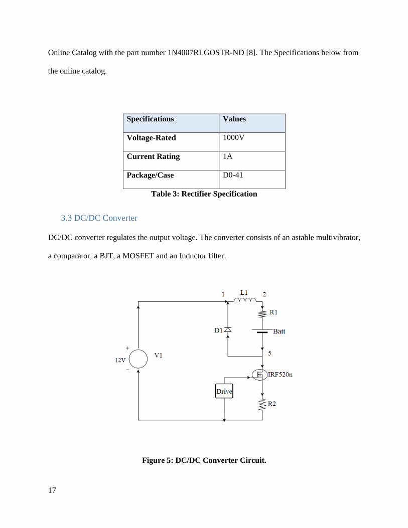
3.3 DC/DC Converter
DC/DC converter regulates the output voltage. The converter consists of an astable multivibrator,
a comparator, a BJT, a MOSFET and an Inductor filter.
Figure 5: DC/DC Converter Circuit.
Page 19
18
For the voltage regulator to be able to handle these higher voltages, I will be using a resistor, a
driver, a diode (1N4007RLG), a BJT, Inductor filter and power MOSFET, which essentially acts
as a high power voltage divider.
3.3.1 Astable Multivibrator using LM741 OP-AMP
An astable multivibrator is used to generate a triangular wave input to the comparator to create a
pulse-width modulation (PWM) signal. The multivibrator functions through a capacitor,
connected to inverting input of the LM741 OP-AMP, charging and discharging. As the capacitor
charges, the output voltage of the OP-AMP oscillators between the positive and negative rails.
As the output switches, the capacitor continues discharging and charging continuing to generate
the square wave [6].
Figure 6: Timer astable circuit.
Page 20
19
The measured values of the component use in this circuit is:
R = 275 kΩ
R1 = 92 kΩ
R2 = 1MΩ
C1 = 0.01 uF
𝑓𝑓 =1
2𝑅𝑅𝑅𝑅
Equation 1: Frequency of the astable multivibrator [9].
Using the values of R = 275 kΩ and C1 = 0.01uF I got 181.1 Hz.
Figure 7: Timer astable multivibrator output square wave.
Page 21
20
The figure 7 above is the output square wave of the astable multivibrator. The square wave is
needed to be convert to a triangular wave in order to be compare with the control voltage.
Oscillator can also generate a wave similar to a triangular wave.
Figure 8: Timer astable multivibrator capacitor voltage.
The triangular wave produced by the capacitor could also be used to compare with the control
voltage, but before it can be use it need to be amplify and adjust the offset.
3.3.2 Comparator
The purpose of the comparator in figure (10) is to output a square wave of amplitude of 10V and
duty cycle whose value is based on the value of Vcontrol.
Page 22
21
Figure 9: Comparator.
The output of the comparator, VSquare, supplies the switch transistors in the DC/DC converter
with the square wave required for the switching operation. The non-inverting input is a fixed
amplitude and frequency triangular wave, Vtriangular. The inverting input is a DC voltage, Vcontrol.
The duty cycle increases when Vcontrol increases and decreases when Vcontrol decreases. When Vtri
< Vcontrol, VSquare is High (10 volts) and when Vtri >Vcontrol, VSquare is Low (0 volts) [5].
Page 23
22
Figure 10: Comparator input and output waveform. Red is input, blue is control voltage
and green is output.
A triangular wave was compared with a control voltage to produce a square wave. This square
wave is going to the gate of the MOSFET of the DC/DC converter. Depending on if the control
voltage increases or decreases, the square duty cycle will change according to the change of the
control voltage.
3.3.3 BJT
The PWM from the comparator is the input to BJT which allows the MOSFET to switch. The
BJT allows the MOSFET to switch faster by conducting a greater amount of current than that
could be supplied by the output of the comparator. When the BJT is ON, the gate of the
MOSFET is charged and the MOSFET turns ON [1].
Page 24
23
3.3.4 MOSFET
An IRF520 N-Channel power MOSFET was used to control the switch of the battery charger.
The gate of the MOSFET is being driven by a pulse – width modulated (PWM) signal to
minimize power losses in the circuit. The duty cycle of the control signal determines the average
DC voltage applied to the battery charger, thus controlling the switches. The diode in the circuit
is a “feel-wheeling diode” to provide a path for the induced charger current to flow, when the
MOSFET turn OFF. Without this diode, a high voltage spike would occur across the MOSFET
during turn-off and would damage or MOSFET [1].
Figure 11: MOSFET and BJT
3.3.5 Filter Inductor
The current in the inductor cannot change instantaneously. This property helps the inductor to
filter out the current ripple and obtain a more constant charging current flow into the battery. In
this project, we use part of a transformer secondary winding as the filter inductor, measured
value of 100 mH. This results an average charging current that is 1A.
Page 25
24
Figure 12: Filter inductor output
The inductor needs to have a minimum value to result a continuous current flow. Given the
switching frequency of the driver circuit as 1000Hz, we can use the following equation to
calculate the minimum inductance value,
𝐿𝐿𝑚𝑚𝑚𝑚𝑚𝑚 =(1 − 𝐷𝐷)𝑅𝑅
2𝑓𝑓
Where R is the equivalent load resistance value. In this study, we have the load modeled as the
battery voltage source in series with its internal resistance. It is necessary to account that in the
minimum inductor value calculation. Nevertheless, the 100mH inductor will ensure the
continuous current flow under all the possible operating conditions, both in theory as well as in
the actual tests [1].
Page 26
25
4. CHAPTER 4: Module Simulation
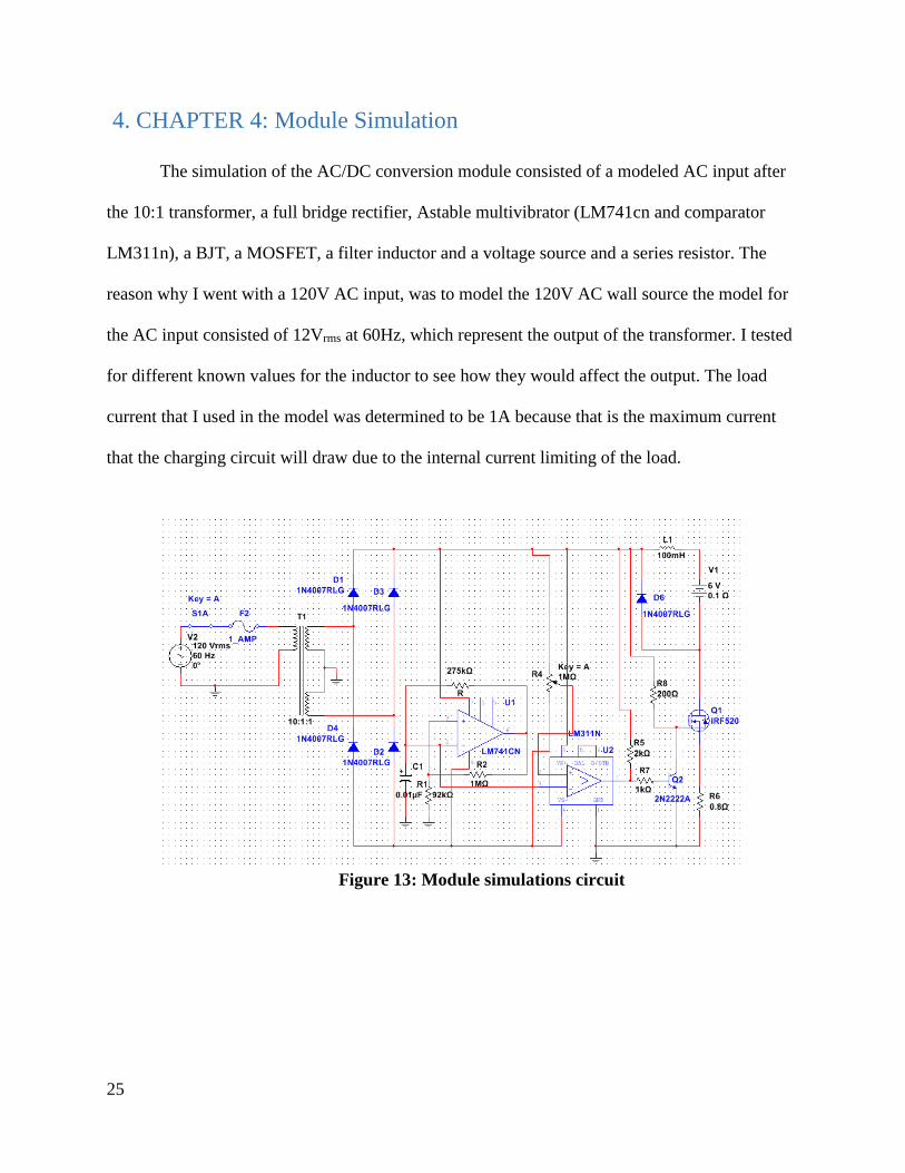
The simulation of the AC/DC conversion module consisted of a modeled AC input after
the 10:1 transformer, a full bridge rectifier, Astable multivibrator (LM741cn and comparator
LM311n), a BJT, a MOSFET, a filter inductor and a voltage source and a series resistor. The
reason why I went with a 120V AC input, was to model the 120V AC wall source the model for
the AC input consisted of 12Vrms at 60Hz, which represent the output of the transformer. I tested
for different known values for the inductor to see how they would affect the output. The load
current that I used in the model was determined to be 1A because that is the maximum current
that the charging circuit will draw due to the internal current limiting of the load.
Figure 13: Module simulations circuit
Page 27
26
4.1 Multisim Result
I modeled the circuit in Multisim and performed the simulation to confirm the circuit behavior.
The rectifier simulation produced a positive polarity DC waveform of 15V. This was what I
expected but the voltage was supposed to be 12V. The output waveform astable oscillator and of
the comparator were measured. The oscillator produced a triangular wave of about 0.9V peak-
to-peak and the comparator produced a square wave output of 5V. Both waves had frequencies
of slightly less than 200Hz.
Figure 14: Rectifier DC waveform
Page 28
27
Figure 15: Oscillator and Comparator
4.2 PSpice Simulation
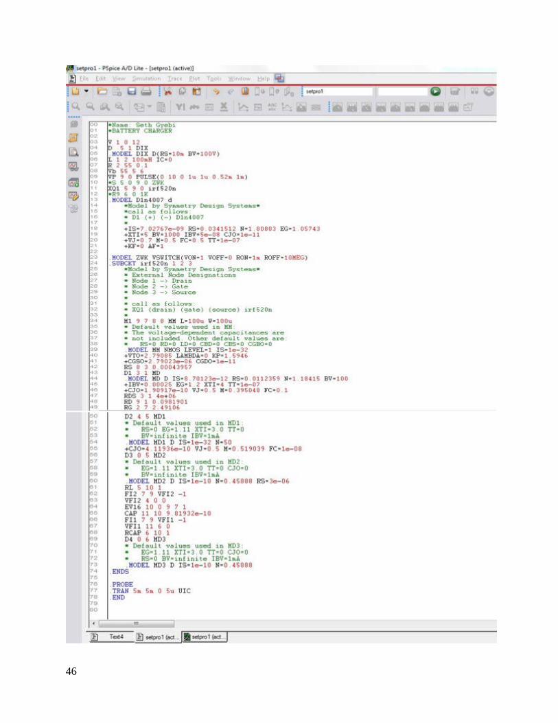
I modeled the circuit in Pspice and performed the simulation to confirm the circuit behavior.in
the Pspice code I used the following nodes to measure from as shown in figure 16. The Pspice
code can be found in the Appendix A.
Page 29
28
Figure 16: Pspice simulation circuit
4.3 Pspice Result
In the Pspice simulations, I measured the current through the inductor between nodes 1 and node
2. The result was a triangular wave of 31mA and frequency of 1000Hz.
Page 30
29
Figure 17: Simulated waveform for the current inductor.
The voltage across the inductor was a square waveform from -6.8V to +6V and a frequency of a
1000Hz.
Figure 18: Simulated waveform for voltage of the inductor
Page 31
30
The voltage across the load and inductor was a square waveform from -0.8V to +12V and a
frequency of a 1000Hz
Figure 19: Simulated waveform for the voltage of the diode, inductor and the load.
The voltage across the load was about 6V with a triangular volt ripple 0.003V and a frequency of
a 1000Hz.
Page 32
31
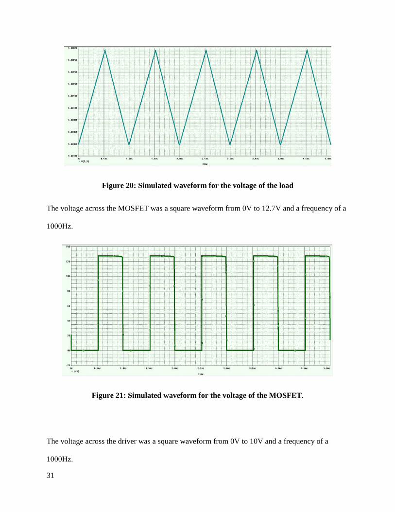
Figure 20: Simulated waveform for the voltage of the load
The voltage across the MOSFET was a square waveform from 0V to 12.7V and a frequency of a
1000Hz.
Figure 21: Simulated waveform for the voltage of the MOSFET.
The voltage across the driver was a square waveform from 0V to 10V and a frequency of a
1000Hz.
Page 33
32
Figure 22: Simulated waveform for the voltage of the driver
The current between the inductor and a diode was a waveform from 0A to 30mA and a
frequency of a 1000Hz.
Figure 23: Simulated waveform current between diode
Page 34
33
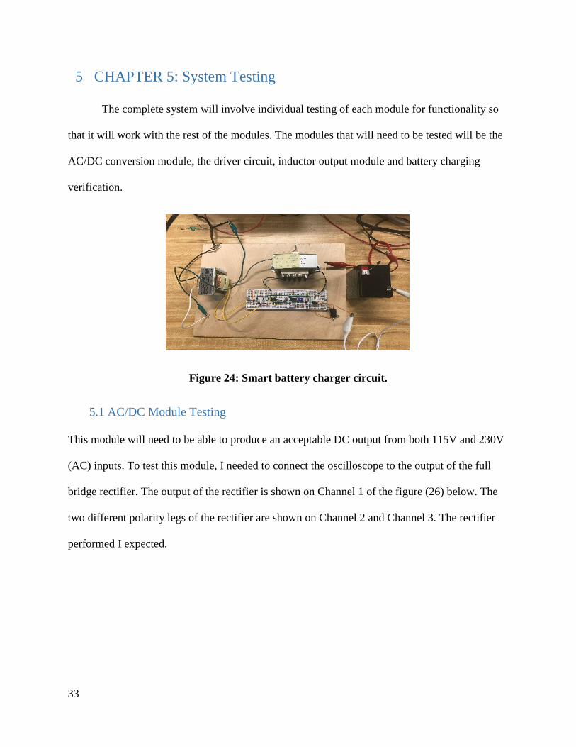
5 CHAPTER 5: System Testing
The complete system will involve individual testing of each module for functionality so
that it will work with the rest of the modules. The modules that will need to be tested will be the
AC/DC conversion module, the driver circuit, inductor output module and battery charging
verification.
Figure 24: Smart battery charger circuit.
5.1 AC/DC Module Testing
This module will need to be able to produce an acceptable DC output from both 115V and 230V
(AC) inputs. To test this module, I needed to connect the oscilloscope to the output of the full
bridge rectifier. The output of the rectifier is shown on Channel 1 of the figure (26) below. The
two different polarity legs of the rectifier are shown on Channel 2 and Channel 3. The rectifier
performed I expected.
Page 35
34
Figure 25: AC/DC Module testing.
Figure 26 : Measured waveform for the output rectifier and the polarity legs of the
rectifier.
Page 36
35
5.2 Driver Circuit Testing
The output of the oscillator and comparator were measured on the oscilloscope. The oscillator
was shown the output of triangular waveform bounded by a sinusoidal envelope. The highest
value of the triangular waveform seemed to be limited by the rail voltage of the op-amp.
Figure 27: Measured oscillator output.
The output of the comparator was a PWM square wave of approximately 0.8V.
Figure 28: Measured comparator output.
Page 37
36
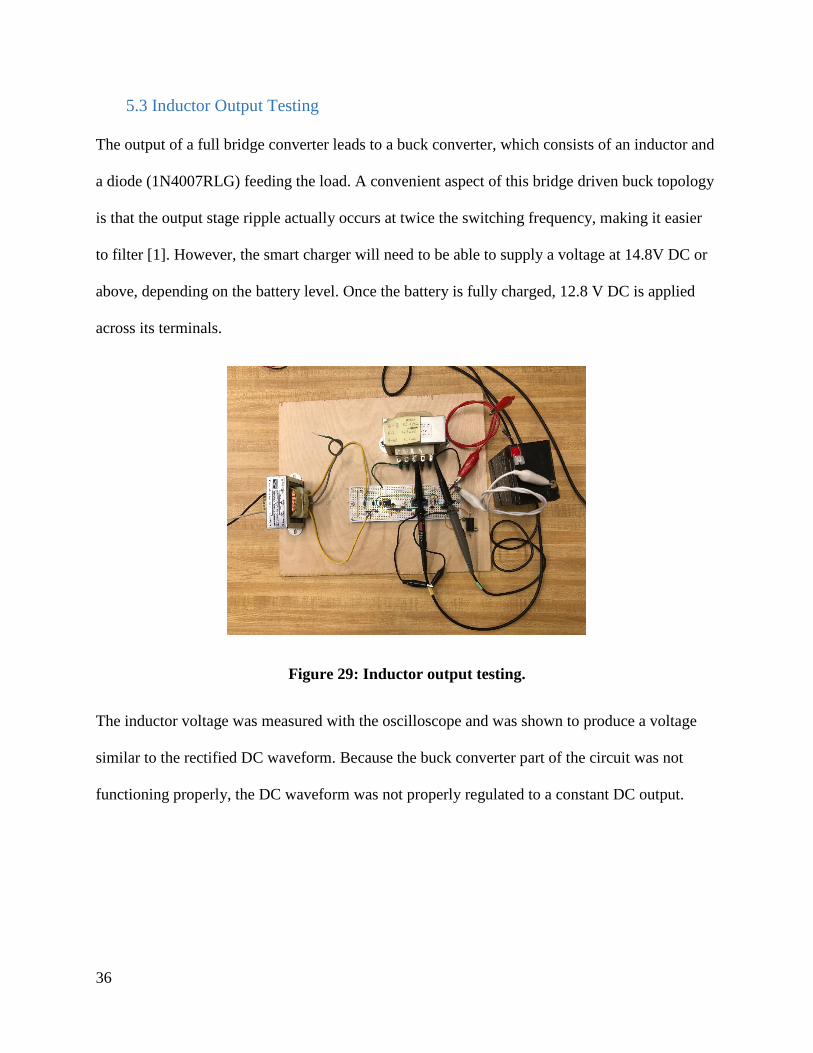
5.3 Inductor Output Testing
The output of a full bridge converter leads to a buck converter, which consists of an inductor and
a diode (1N4007RLG) feeding the load. A convenient aspect of this bridge driven buck topology
is that the output stage ripple actually occurs at twice the switching frequency, making it easier
to filter [1]. However, the smart charger will need to be able to supply a voltage at 14.8V DC or
above, depending on the battery level. Once the battery is fully charged, 12.8 V DC is applied
across its terminals.
Figure 29: Inductor output testing.
The inductor voltage was measured with the oscilloscope and was shown to produce a voltage
similar to the rectified DC waveform. Because the buck converter part of the circuit was not
functioning properly, the DC waveform was not properly regulated to a constant DC output.
Page 38
37
5.4 Final battery charging verification
When tested the battery charger circuit did not work as expected. The output to the battery
appeared to charge at only about 20mA and the output voltage was shown to be similar to the
rectifier DC waveform. To determine the cause of this problem, the outputs of the astable
multivibrator and comparator were measured, and no PWM signal was being generated. This
was likely due to how the op-amp and comparators were being powered. The rail voltages were
supplied by the rectified DC instead of from a constant DC source. If the rails were powered by
DC, the driver PWM signal may have been generated properly.
Figure 30: Battery charger verification
Page 39
38
6 Conclusion
My project was a Smart battery charger to charge a sealed lead-acid battery. My goal was to
design, simulate, and build a Smart battery charger. The circuit was simulated in Pspice to verify
design before construction. A prototype circuit board was built and all components soldered by
hand, including a high frequency transformer and inductor. Testing, revision, and analysis of the
completed circuit board was performed. The result was successful.
Page 40
39
7 References
[1] Hart DW. Power electronics. 1st ed. New York, NY: McGraw, Hill; 2011:439.
[2] Power transformer 24vct@1A 115/230VAC wire leads. http://www.jameco.com Web site.
http://www.jameco.com/z/102111-R-Power-Transformer-24vct-1A-115-230VAC-Wire-
Leads_102112.html. Accessed Mar 24, 2017.
[3] Gleyzer V, Masullo S, Mulla J. Design and integration. WORCESTER POLYTECHNIC
INSTITUTE. 2003:1-20.
[4] Apollonio B, king C, Murray S. Unity power factor universal batterry charger. WORCESTER
POLYTECTNIC INSTITUTE. 2006:1-112.
[5] Le NT, Sbat A. Solar battery charger. WORCESTER POLTECHNIC INSTITUTE. :10-39.
[6] Brahma Chary PS. Operational amplifier as astable multivibrator. GOVERNMENT
POLYTECHNIC KOTHAGUDEM Web site.
http://kothagudemgovtpoly.nic.in/StudentsCorner/StudentsCorner117.pdf.
Accessed Mar 17, 2017.
[7] Surge protector. wikipedia.org Web site. https://en.wikipedia.org/wiki/Surge_protector.
Updated 2017. Accessed 12 March, 2017.
[8] ON semiconductor 1N4007RLG. Digikey, Web site. https://www.digikey.com/product-
detail/en/on-semiconductor/1N4007RLG/1N4007RLGOSTR-ND/918021. Accessed Mar 24,
2017.
Page 41
40
[9] Op-amp multivibrator. electronics-tutorials.ws Web site. http://www.electronics-
tutorials.ws/opamp/op-amp-multivibrator.html. Accessed Mar 24, 2017.
Page 42
41
Appendix A
*Name: Seth Gyebi
*BATTERY CHARGER
V 1 0 12
D 5 1 DIX
.MODEL DIX D (RS=10m BV=100V)
L 1 2 100mH IC=0
R 2 55 0.1
Vb 55 5 6
VP 9 0 PULSE (0 10 0 1u 1u 0.52m 1m)
*S 5 0 9 0 ZWK
XQ1 5 9 0 irf520n
*R9 6 0 1K
.MODEL D1n4007 d
*Model by Symmetry Design Systems*
*call as follows:
* D1 (+) (-) D1n4007
Page 43
42
*
+IS=7.02767e-09 RS=0.0341512 N=1.80803 EG=1.05743
+XTI=5 BV=1000 IBV=5e-08 CJO=1e-11
+VJ=0.7 M=0.5 FC=0.5 TT=1e-07
+KF=0 AF=1
.MODEL ZWK VSWITCH (VON=1 VOFF=0 RON=1m ROFF=10MEG)
.SUBCKT irf520n 1 2 3
*Model by Symmetry Design Systems*
* External Node Designations
* Node 1 -> Drain
* Node 2 -> Gate
* Node 3 -> Source
*
* call as follows:
* XQ1 (drain) (gate) (source) irf520n
*
M1 9 7 8 8 MM L=100u W=100u
Page 44
43
* Default values used in MM:
* The voltage-dependent capacitances are
* not included. Other default values are:
* RS=0 RD=0 LD=0 CBD=0 CBS=0 CGBO=0
.MODEL MM NMOS LEVEL=1 IS=1e-32
+VTO=2.79085 LAMBDA=0 KP=1.5946
+CGSO=2.79023e-06 CGDO=1e-11
RS 8 3 0.00043957
D1 3 1 MD
.MODEL MD D IS=8.70123e-12 RS=0.0112359 N=1.18415 BV=100
+IBV=0.00025 EG=1.2 XTI=4 TT=1e-07
+CJO=1.90917e-10 VJ=0.5 M=0.395048 FC=0.1
RDS 3 1 4e+06
RD 9 1 0.0981901
RG 2 7 2.49106
D2 4 5 MD1
* Default values used in MD1:
* RS=0 EG=1.11 XTI=3.0 TT=0
Page 45
44
* BV=infinite IBV=1mA
.MODEL MD1 D IS=1e-32 N=50
+CJO=4.11936e-10 VJ=0.5 M=0.519039 FC=1e-08
D3 0 5 MD2
* Default values used in MD2:
* EG=1.11 XTI=3.0 TT=0 CJO=0
* BV=infinite IBV=1mA
.MODEL MD2 D IS=1e-10 N=0.45888 RS=3e-06
RL 5 10 1
FI2 7 9 VFI2 -1
VFI2 4 0 0
EV16 10 0 9 7 1
CAP 11 10 9.81932e-10
FI1 7 9 VFI1 -1
VFI1 11 6 0
RCAP 6 10 1
D4 0 6 MD3
* Default values used in MD3:
Page 46
45
* EG=1.11 XTI=3.0 TT=0 CJO=0
* RS=0 BV=infinite IBV=1mA
.MODEL MD3 D IS=1e-10 N=0.45888
.ENDS
.PROBE
.TRAN 5m 5m 0 5u UIC
.END