A Smart Battery Management System for Electric Vehicles using Powerline Communication
135
Institute for Data Processing Technische Universität München Master’s thesis A Smart Battery Management System for Electric Vehicles using Powerline Communication Alexander Scherer March 31, 2013
Transcript
Institute for Data ProcessingTechnische Universität München
Master’s thesis
A Smart Battery Management System forElectric Vehicles using Powerline
Communication
Alexander Scherer
March 31, 2013
Alexander Scherer. A Smart Battery Management System for Electric Vehicles using Pow-erline Communication. Master’s thesis, Technische Universität München, Munich, Ger-many, 2013.
Supervised by Prof. Dr.-Ing. K. Diepold and Prof. Dr. T. Bräunl; submitted on March 31,2013 to the Department of Electrical Engineering and Information Technology of the Tech-nische Universität München.
I hereby confirm that I have independently composed this Master’s thesis and that no otherthan the indicated aid and sources have been used. This work has not been presented toany other examination board.
Munich, 31/3/13
Acknowledgements
This thesis would not have been possible without the support of many people.
I wish to thank, first and foremost, my Professor Klaus Diepold. He made me familiarwith Prof. Thomas Bräunl, fundamentally helped shaping the thesis and provided me withexcellent support.
I owe my deepest gratitude to Prof. Thomas Bräunl for giving me the possibility to workon such an interesting topic and for enabling my term abroad in Australia.
I would like to thank Rob Mason for the expert guidance on large battery packs and foroffering his support in conducting measurements on a real-world electric vehicle.
Johannes Mühlfeld, Jeannette Bet and my parents Otto and Annette have made aninvaluable contribution by iteratively discussing and proofreading my thesis.
I cannot find words to express my gratitude to my friends and family who supported meduring my studies and helped me grow in so many ways.
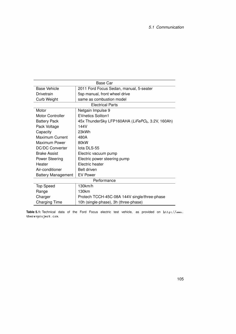
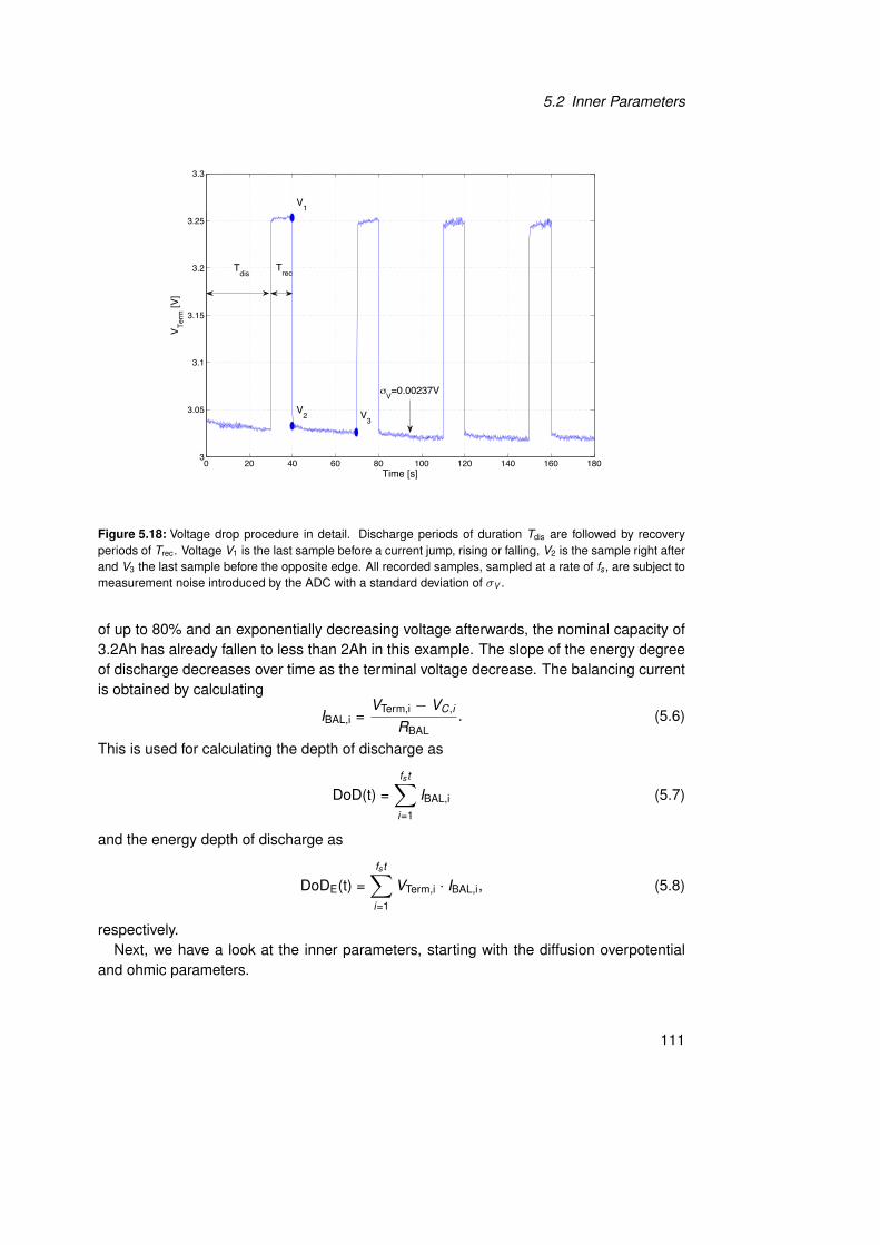
Background. Li-Ion cells reach an outstanding performance, but only if they are main-tained well. Hence, an effective battery management system is needed to maintain abattery pack and to ensure the operation within a safe operating area. For a battery pack,this is typically done by a slave module for each battery block in series which reports cellspecific information to a master device. This is in general achieved via a 1- or 2-wire con-nection resulting in a high installation effort, more knowledge necessary to assemble abattery pack, additional error sources and additional weight. It is examined in this workwhether replacing these wires with powerline communication helps to reduce these prob-lems.Another issue with common battery management systems is their limited capability of ob-taining deep insight into a battery’s condition. This is addressed by developing on-boardtime-domain analysis methods.Methods. A digital experimental verification platform is designed and assembled which isthen connected to a real-world large battery pack of an electric vehicle to conduct commu-nication reliability tests. Inner parameter estimation circuitry is developed and tested in aLiFePO4 cell.Results. Powerline communication is found to achieve a 99.9% success rate of correctlytransmitted packets under the condition of an electric vehicle under load. Time-domainbased inner parameter estimation can help to determine inner battery parameters.Conclusion. Powerline communication and time-domain based inner parameter estima-tion are useful techniques to replace communication wires and to extend common batterymanagement functionality from a technical point of view. These findings can help createsmart batteries which are able to maintain themselves without the need for external de-vices and to communicate their state to the external device it powers by integrating thedeveloped technology into the housing of the cells.
In a world where environmental protection and energy conservation on the one hand andthe growing demand for individual transportation on the other hand are growing concerns,the development of powerful energy storage systems for electric vehicles which are bothcapable of providing high energy- and power densities has taken on an accelerated pace.
Lithium-ion based batteries which are known to possess the highest-in-class energy-and power density, a coulomb efficiency close to 100%, good cycle durability, low self-discharge rates and no memory effect are seen as the most promising battery technologyfor the next years.
However, Li-ion batteries need a relatively high maintenance effort, which even in-creases if multiple cells are assembled in series in order to achieve greater pack voltageswhich are necessary e.g. in electric vehicles. The battery management system’s dualtask is to prevent operation outside each cell’s safe operating area and to balance cells tomaximize storage capacity of the battery pack.
Reporting monitored data demands a means of communication. So far, this has beensolved by 1- or 2-wire communication solutions predominantly.
This work’s intention is to explore to what extend it is possible to omit these wires andreplace them with powerline communication (PLC) in order to save weight and reducewiring complexity and to implement intrinsically safe, self-managing large Li-ion batterypacks.
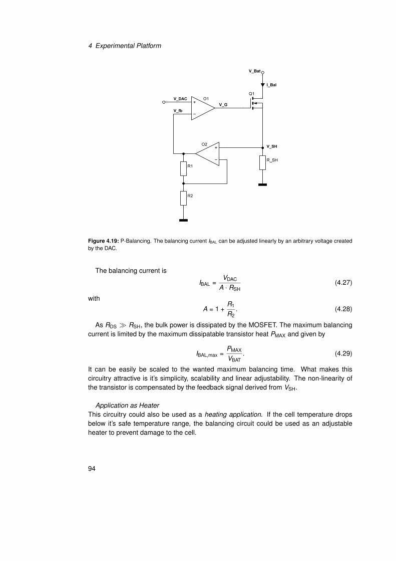
With the Renewable Energy Project1, the Robotics & Automation Lab of The Universityof Western Australia (UWA) makes a great effort to demonstrate that sustainable trans-portation for everybody can be carried out. Students have converted three road-goingpetrol cars into electric vehicles and participate at Formula SAE, an international com-petition for university students to design and race Formula style vehicles. Having beenpowered by combustion engines originally, a new category was introduced for electric ve-hicles in 2008 and UWA as one of the first universities takes on the challenge to rely onelectric instead of combustion engines.
Contributing to this project, this thesis offers a first step towards the ultimate goal bydesigning a microprocessor based powerline communicating battery management systemcircuitry which also meets the Formula SAE rules to allow for testing under race conditions.
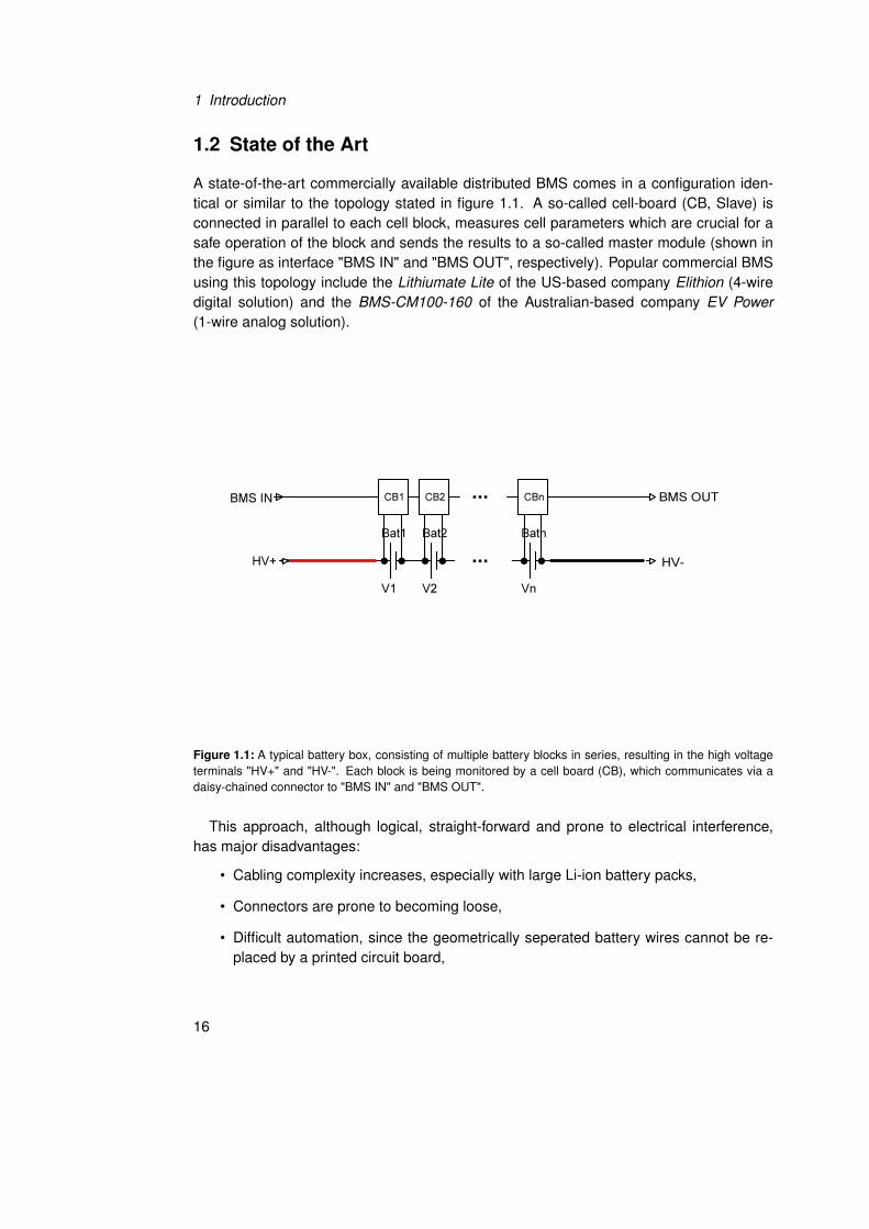
A state-of-the-art commercially available distributed BMS comes in a configuration iden-tical or similar to the topology stated in figure 1.1. A so-called cell-board (CB, Slave) isconnected in parallel to each cell block, measures cell parameters which are crucial for asafe operation of the block and sends the results to a so-called master module (shown inthe figure as interface "BMS IN" and "BMS OUT", respectively). Popular commercial BMSusing this topology include the Lithiumate Lite of the US-based company Elithion (4-wiredigital solution) and the BMS-CM100-160 of the Australian-based company EV Power(1-wire analog solution).
Figure 1.1: A typical battery box, consisting of multiple battery blocks in series, resulting in the high voltageterminals "HV+" and "HV-". Each block is being monitored by a cell board (CB), which communicates via adaisy-chained connector to "BMS IN" and "BMS OUT".
This approach, although logical, straight-forward and prone to electrical interference,has major disadvantages:
• Cabling complexity increases, especially with large Li-ion battery packs,
• Connectors are prone to becoming loose,
• Difficult automation, since the geometrically seperated battery wires cannot be re-placed by a printed circuit board,
16
1.3 Problem Statement
• Cells cannot be made intrinsically safe, as the cell-boards cannot be integrated intothe battery.
The ultimate goal of easy-to-assemble, intrinsically safe battery packs is still hamperedby the disadvantages listed. If there were a possibility to abolish the communication wireswithout losing the ability to communicate, this technology gap could be closed.
An ideal concept to overcome all detriments at once would be Powerline Communica-tion. However, it comes along with its own challenges. The power line channel is a harshand noisy transmission medium which is very difficult to model. It is frequency-selective,impaired by colored background noise and also affected by periodic and aperiodic impulsenoise (Dostert, 2012), (Biglieri, 2003). The powerline channel is also time-varying, i.e.the channel transfer function may vary abruptly when the topology changes, that is, whendevices are switched on or off. A fundamental property of the powerline channel in an elec-tric vehicle is that the time-varying behavior mentioned before is a periodically time-varyingbehavior, where the frequency of the variation is a multiple of the engine revolution speed.Additional challenges are due to the fact that power line cables are often unshielded andthus become "both a source and a victim of electromagnetic interference" and must there-fore include "mechanisms to ensure successful coexistence with wireless [...] systems", aswell as "be robust with respect to impulse noise and narrow band interference" (Galli andLogvinov, 2008). Also, the low resistance of battery packs which can fall below 1m, canmake transmission a challenge.
"Interest has mostly been directed toward using AC power lines to promote commu-nication between appliances, computers and equipment within and between buildings.Less attention has been directed toward DC power lines, which are used in vehicles", YairMaryanka, inventor of the US patent "Signaling over noisy channels", (Maryanka, 2006),granted in May 2006, formulated and took action to adapt schemes to DC power lines.From former research activities, represented in another patent (Maryanka, 1998), whichdeals with "high-speed transmission of data over DC power lines with error control bymeans of channel coding and modulation", he invented the microchip SIG60, which isfurther examined and used in this thesis.
1.3 Problem Statement
Several steps are taken to analyze the viability of Powerline Communications in BatteryManagement Systems.
First, a general description of Li-Ion batteries and their properties is given with focus ontheir electrical behavior.
Next, the functionality of a battery management system will be discussed in detail andpossible functional impairments due to the restricted number of connectors with the PLCsolution will be outlined.
Subsequently, a powerline communication solution is characterized and fitted to work
17
1 Introduction
with a typical Li-Ion Battery Pack as used in electric vehicles. Requirements of a testplatform are defined and the findings are transferred into a hardware design.
Three prototypes of the resulting BMS Slaves are manufactured and assembled. Afirmware, offering a basic set of console instructions for access through a serial PC inter-face is developed.
The three developed slaves are applied in a 2-cell LiFePO4 battery setup with two slavesacting as slave modules and one slave acting as the master module, as shown in figure 1.2.A successful function of this setup proves the general viability of powerline communicationfor battery management applications.
Figure 1.2: Two-cell setup. Two prototype boards work as slaves (CB1 and CB2) while the other one worksas the master, proving that an effective battery management system using the battery poles only is feasible.
To face the problem of insufficient knowledge about the battery internal parameters, cir-cuitries to achieve electrochemical impedance spectroscopy-like results without the needfor external power supplies are discussed. The most suitable solution is realized in hard-ware on an experimental verification platform and tested on a LiFePO4 cell. The problemis solved when it is possible to determine all primary parameters for a given equivalentelectrical circuit.
18
1.4 Research Goals
1.4 Research Goals
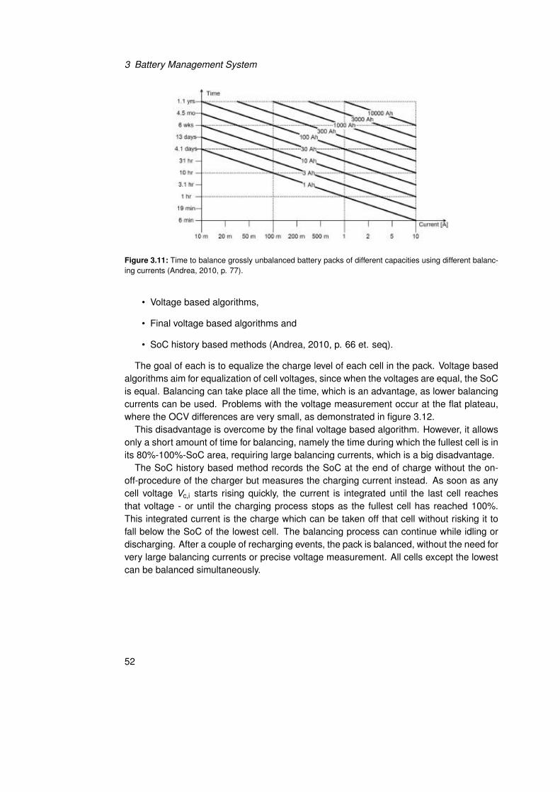
The main hypothesis being explored in this thesis is to what extend distributed BatteryManagement Systems can abdicate communication wires by using the battery power lineas the communication medium. Open questions to be answered include:
• To what extend can cheap on-board battery-powered generic ICs replace pro-fessional self-powered Electrochemic Impedance Spectroscopy measurement de-vices?
• Can these additional measurements contribute to an accurate state of health es-timation on cell level and can deviations in cell impedance help to develop anearly-warning system of imminent faults and thus significantly improve battery packsafety?
• Is PLC a viable alternative to existing 1- and 2-wire BMS solutions?
The experimental verification platform to be built contains hardware
1. to realize an effective battery management system,
2. to realize electrochemical impedance spectroscopy-like functionality and
3. a powerline communication interface.
The largest potential application are road-going passenger automobiles of which there arecurrently over 700 million worldwide. However, for this project the available test vehicleand first application of the research will be a Formula SAE Electric vehicle.
1.5 Thesis Guide
The thesis is subdivided into 5 parts.
Chapter 2 deals with a characterization of Lithium Batteries from an electrical point ofview. Basic definitions are given. Similarities and differences between several commonlyused chemistries, their correct handling and their advantages and disadvantages forseveral applications are pointed out. After carving how to handle a single cell, we havea look at methods to connect many cells into a larger battery pack. We point out thepossibilities these packs can offer but also their dangers when operating them outsidetheir safe operation area and clearly state the essential need for a Battery ManagementSystem.
Chapter 3 focuses on Battery Management Systems and starts by defining their tasks.Two basic topologies (localized and distributed) are presented and compared. We will
19
1 Introduction
have an in-depth look at active and passive balancing technologies and also proceduresto derive battery internal parameters, which are typically hidden from the outside and areonly accessible by destruction of the cell or by electrical measurements.
Drawing from the knowledge revised in the previous two chapters, Chapter 4 dealswith the practical design of our own improved Battery Management System. Focusedon the improvements (Powerline communication and internal state determination), thearchitecture is revealed and design decisions made are justified.
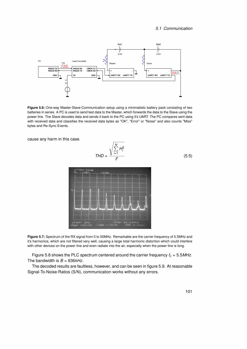
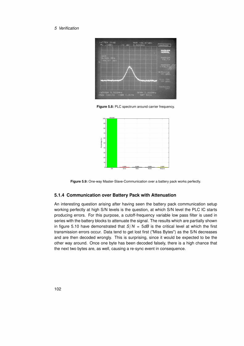
Chapter 5 is about test benching the newly made BMS. Is powerline communicationreliable
• for battery packs of different sizes?
• for idling as well as for driving conditions?
How accurate are inner parameter estimations? Can they be used to derive secondaryparameters like State of Charge or State of Health?
Chapter 6 concludes the work and gives an outlook to whether it is useful to pursue theinitially proposed way and which further challenges need to be faced in order to achievethe ultimate goal.
20
2 Batteries
First of all, it is important to define and understand the devices that are being used asboth a means of communication and source of electricity: electrochemical cells. In thischapter, the functional principle of a galvanic cell is revised. Next, we discuss its generalmode of operation with a brief look at cell chemistries and chemical reactions. Then, thecharging and discharging process are examined and explained and important equationslike the Butler-Volmer-equation are presented. This theoretical background will build thefundament for deriving an electrochemical equivalent electrical circuit later, which we canuse to characterize a battery by measurement in the later chapters. Lithium Iron Phosphatecells are given a high priority since those are the most promising solution mostly becausethey yield a great performance.
2.1 Electrochemical Cell
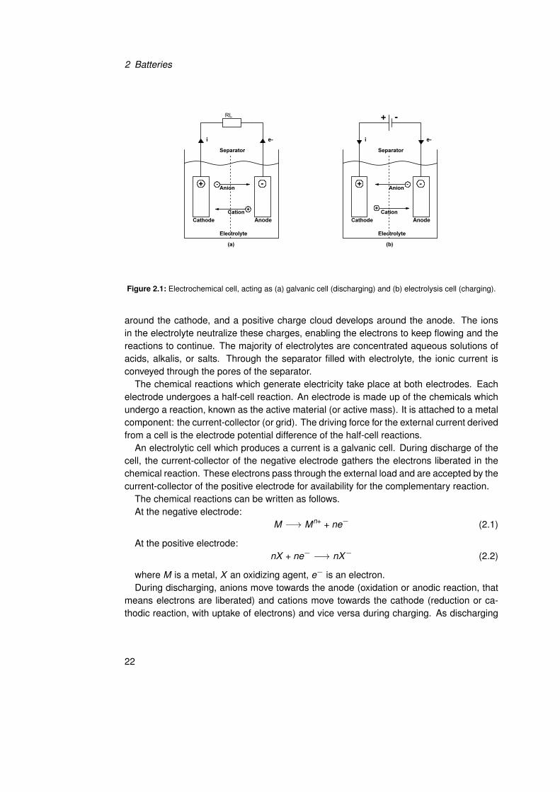
What characterizes an electrochemical cell? In general, it is a chemical device to generateand store electricity. An electrolytic cell is shown schematically in figure 2.1. The essentialcomponents are
• a positive electrode (cathode),
• a negative electrode (anode),
• an electrolyte,
• a separator and
• a housing.
The electrodes have to be as close to each other as possible to minimize the internalresistance of the cell.
The separator is a thin, usually porous, insulating material which prevents short-circuiting of the electrodes when they come in close contact. The pores of the separatorare filled with electrolyte, which is capable of conducting ions between two electrodes, butwhich itself is an electronic insulator. Loose electrons normally cannot pass through theelectrolyte. Instead, a chemical reaction occurs at the cathode consuming electrons fromthe anode. Another reaction occurs at the anode, producing electrons that are eventuallytransferred to the cathode. As a result, a negative charge cloud develops in the electrolyte
21
2 Batteries
Figure 2.1: Electrochemical cell, acting as (a) galvanic cell (discharging) and (b) electrolysis cell (charging).
around the cathode, and a positive charge cloud develops around the anode. The ionsin the electrolyte neutralize these charges, enabling the electrons to keep flowing and thereactions to continue. The majority of electrolytes are concentrated aqueous solutions ofacids, alkalis, or salts. Through the separator filled with electrolyte, the ionic current isconveyed through the pores of the separator.
The chemical reactions which generate electricity take place at both electrodes. Eachelectrode undergoes a half-cell reaction. An electrode is made up of the chemicals whichundergo a reaction, known as the active material (or active mass). It is attached to a metalcomponent: the current-collector (or grid). The driving force for the external current derivedfrom a cell is the electrode potential difference of the half-cell reactions.
An electrolytic cell which produces a current is a galvanic cell. During discharge of thecell, the current-collector of the negative electrode gathers the electrons liberated in thechemical reaction. These electrons pass through the external load and are accepted by thecurrent-collector of the positive electrode for availability for the complementary reaction.
The chemical reactions can be written as follows.At the negative electrode:
M ! Mn+ + ne (2.1)
At the positive electrode:nX + ne ! nX (2.2)
where M is a metal, X an oxidizing agent, e is an electron.During discharging, anions move towards the anode (oxidation or anodic reaction, that
means electrons are liberated) and cations move towards the cathode (reduction or ca-thodic reaction, with uptake of electrons) and vice versa during charging. As discharging
22
2.2 Lithium Iron Phosphate Accumulator
is the common mode of operation of a battery, the negative electrode if often known asthe anode and the positive electrode as the cathode, which is the exact opposite of theconvention for electrolysis. To avoid confusion, we stick with the terms of negative andpositive electrodes.
Typical metals which form the negative active-mass are cadmium (Cd), lead (Pb) orlithium (Li), whereas popular positive active-mass materials are nickel (NiOOH), lead(PbO2) and manganese (MnO2), cobalt (CoO2) or iron (FePO4). These different possi-bilities for the active materials are referred to as different cell chemistries (Dell et al., 2001,p. 10 et. seq).
As an example of an electrochemical cell we present the LiFePO4 accumulator next.
2.2 Lithium Iron Phosphate Accumulator
Two of the most promising compounds are lithium metal phosphates. Especially the olivinestructured triphylite LiFePO4, which was first proposed by Padhi et al. in 1997 (Padhi et al.,1997), seems suitable. Its redox potential vs. Li /Li+ is 3.4V whereas the theoretical ca-pacity accounts for 170mAh/g. One reason for its superior potential is that iron, the redoxactive species in this material, has a comparatively high Clarke number. The Clarke num-ber is an estimation of the abundance of an element in the outermost shell of the earth.Due to its high score iron is considered to be among the five most common elements in theearth crust. In consequence, LiFePO4 is a potentially low priced active material. Further-more, it is nontoxic, environmentally benign and less prone to oxygen loss compared toother oxide based cathode materials thus ensuring high safety. Yet, LiFePO4 has a majordisadvantage: Its intrinsic electronic conductivity is only 109S/cm (Jüstel et al., 2012).However, these properties make this type of accumulator the first choice for many electricvehicle applications. That is why we focus on this particular chemistry with the followingchemical reactions involved:
Positive electrode:
LiFe(II)PO4charge
dischargeFe(III)PO4 + Li+ + e (2.3)
Negative electrode:
Li+ + echarge
dischargeLi (2.4)
Lithium on the one hand is extracted from LiFePO4 to charge the positive electrode andon the other hand is inserted into FePO4 on discharge. The standard electrode potentialdifference for this chemistry is E0 = 3.4V . A corresponding half cell is shown in figure 2.2.
Having analysed the chemical reaction in equilibrium, we next review their behaviourwhile charging and discharging.
23
2 Batteries
Electrochemical Impedance Spectroscopy of a LiFePO4/Li Half-Cell Mikael Cugnet*, Issam Baghdadi and Marion Perrin French Institute of Solar Energy (INES), CEA / LITEN *Corresponding author: 50 Avenue du lac Léman, 73377 Le Bourget-du-Lac, France, [email protected] Abstract: This study demonstrates that a multiphysical model of a LiFePO4/Li half-cell can be applied to simulate the impedance results from an EIS. However, it implies that the double layer capacitance has to be taken into account, since it is responsible of the semi-circle in the impedance spectrum. A 15 min simulation allows getting a complete spectrum of the half-cell impedance from 0.1 to 200 kHz. The methodology used to adjust the three key parameters used to fit the experimental data is described. However, this work is still in progress, so we do not know exactly yet what is actually responsible of the slope observed at lower frequencies. There might be a missing phenomenon somewhere in our model or some parameter values still to be adjusted. Keywords: Lithium-ion batteries, LFP/Li coin cell, Electrochemical Impedance Spectroscopy. 1. Introduction
Li-ion battery models designed with Comsol Multiphysics are usually intended for simulating the battery behavior during a period of time going from few minutes to many hours. However, most of Li-ion battery models designed today are based on equivalent circuit models. These models are composed of electrical components (resistances, inductances, capacitances…) whose values are identified when the battery is at equilibrium by an experimental method called “Electrochemical Impedance Spectroscopy” (EIS). Therefore, we tried to simulate a model of a LiFePO4/Li half-cell, for which we had EIS experimental data, in order to see if our model was also able to simulate the battery behavior for frequencies going from 100 mHz to 200 kHz. 2. Model of the LiFePO4/Li half-cell
A schematic of the LiFePO4/Li half-cell studied in this work is presented in Fig. 1. The lithium foil used as the counter electrode is also the reference electrode.
Figure 1. Schematic of the LiFePO4/Li half-cell
The model used to simulate the half-cell is
based on the most recent publications [1-5]. The reaction (1) occurs at the working electrode (iron phosphate) 44 LiFePOFePOeLi ↔++ −+ , (1) and the reaction (2) occurs at the counter electrode (lithium foil) LieLi ↔+ −+ . (2)
Our 1D macroscopic model of the half-cell is made up of two domains. The first one is the separator and the second one is the positive electrode (iron phosphate). The negative electrode (lithium foil) is the first boundary on the left. The second boundary is the interface between the separator and the positive electrode. The third boundary is the interface between the positive electrode and the carbon-coated aluminum current collector.
Our 1D microscopic model of the iron phosphate spherical secondary particle is made up of one domain and two boundaries, respectively for the surface and the center of the particle. 3. Governing equations
The model is composed of four equations and two dimensions depending of the scale considered. The dimension x represents the distance to the lithium foil and the dimension r the distance from the center of the particle.
Figure 2.2: LiFePO4/Li half-cell (COMSOL et al.).
2.3 Cell Discharging and Charging
The voltage of a cell measured under load (when drawing current) will be lower than theopen circuit voltage (OCV). This results from the internal impedance of the battery whichconsists of:
• polarization losses at the electrodes and
• resistive (ohmic) IR losses in the grids, electrolyte and active masses.
When current flows through a battery, there is deviation from equilibrium conditions andthe performance is lessbelow its maximum. The shift in potential of an electrode away fromthe reversible (equilibrium) value is termed the electrode overpotential (). This overpo-tential is built up of two components:
• an activation overpotential caused by kinetic limitations of the charge-transfer pro-cess at the electrode. This is an intrinsic property of the electrode material immersedin the electrolyte, i.e. an interface phenomenon.
• A concentration overpotential which results from depletion of reactants in the proxim-ity of the electrode due to slow diffusion from the bulk solution or across the productlayer. This is an extensive property that depends on the thickness and porosity ofthe electrode and the ease of diffusion through it, as well as upon mass-transportprocesses in the electrolyte.
Taken together, these two overpotentials result in a voltage drop at the electrode duringdischarging, the so-called polarization loss, and the electrode is known to be polarized.
24
2.3 Cell Discharging and Charging
Similarly, the voltage drop due to the internal resistance of the battery is commonly referredto as resistance, ohmic polarization or overpotential.
When charging the battery, the reverse processes take place, with diffusion controllingboth the macroscopic and the microscopic reaction paths within the active mass.
Polarization losses occur at each electrode and are responsible for a decreased cellvoltage during discharge (Vd ) and an increased cell voltage when charging (Vch)):
Vd = Vr + IR (2.5)
Vch = Vr + + + + IR (2.6)
where + and are the overpotentials at the positive and negative electrodes. Thisequation reduces to Ohm’s Law for low overpotentials:
Vd = Vr IR0 (2.7)
Vch = Vr + IR0 (2.8)
where R0 is the sum of the internal resistances of the cell and the equivalent resistancesof the activation and concentration overpotentials at both electrodes. The correlation be-tween the practical cell voltage is shown schematically in figure 2.3. An electrical equiv-alent circuit of the discussed resistances is given in figure 2.4 which is related to (Wenzl,2006). In the equivalent circuit,
• V + V is the OCV,
• Rs is the resistance of the seperatar and the electrolyte,
• R+p and R
p are the polarization overpotential impedances,
• R+am and R
am are the resistances of the active masses of both electrodes,
• R+t and R
t are the transition resistances,
• R+p and R
p are the pole and grid resistances and
• RL is the external load.
Figure 2.4 models the cell in one dimension. It is possible to extend the model to a 2Dmodel which also takes care of the width of the electrodes but not the thickness (figure2.5). The longer the electrode and the larger the pole resistances and currents, the higherare inhomogenities in the current.
It has been shown that the desired degree of detail is responsible for the complexity ofthe model used. But before deducting which model is suited best for our purposes, it isuseful to learn more about how the overpotential depends on the current density of theelectrodes. These correlations are defined in the Butler-Volmer- and the Nernst-Equation.
25
2 Batteries
Figure 2.3: Schematic representation of the relation between practical cell voltages and reversible cell voltage(Dell et al., 2001, p. 17).
Figure 2.4: Electrical Equivalent Circuit showing the internal sources and resistances of a electrochemical cell(Wenzl, 2006).
The Butler-Volmer equation is one of the most fundamental connections in electrochemicalkinetics. It describes how the electrical current on an electrode depends on the electrodepotential considering that both a cathodic and an anodic reaction occur at the same elec-trode. It is mostly written as
I = A · i0 ·
exp↵anFRT
(E Eeq) exp
↵cnF
RT(E Eeq)
, (2.9)
where
• I is the electrode current [A],
• A is the electrode active surface area [m2],
• i0 is the exchange current density [ Am2 ],
• E is the electrode potential [V],
• Eeq is the equilibrium potential [V],
• T is the absolute temperature [K],
• n is the number of electrons involved in the electrode reaction,
• F is the Faraday constant: F = 9.648 · 104 Cmol ,
• R is the universal gas constant: R = 8.314 JK ·mol ,
• ↵c is the cathodic charge transfer coefficient [1] and
• ↵a is the anodic charge transfer coefficient [1] (Wikipedia).
The term = E Eeq is called activation overpotential. This overpotential depends onthe electrode current. This is important because this dynamic effect can be measured andmodelled.
The equilibrium potential is derived from the Nernst equation, as presented next.
2.5 Nernst-Equation
The following Nernst-Equation is used to determine equilibrium reduction potential of ahalf-cell in an electrochemical cell. It is also used to determine the total voltage (electro-motive force) for a full electrochemical cell.
Ered = Ered
RTzF
lnaRed
aOx(2.10)
27
2 Batteries
as the half-cell reduction potential or
Ecell = Ecell
RTzF
ln Q (2.11)
as the total cell potential, where
• Ered is the half-cell reduction potential at the temperature of interest [V],
• Ered is the standard half-cell reduction potential [V],
• Ecell is the standard cell potential at the temperature of interest [V],
• R is the universal gas constant: R = 8.314 JK ·mol ,
• T is the absolute temperature [K],
• a is the chemical activity for the relevant species, where aRed is the reductant andaOx is the oxidant,
• F is the Faraday constant: F = 9.648 · 104 Cmol ,
• z is the number of moles of electrons transferred in the cell reaction of half-reactionand
• Q is the reaction quotient.
The Nernst equation relates the numerical values of the concentration gradient to theelectric gradient that balances it.
2.6 Equivalent Electrical Circuit
Electrical models are typically used to model
• the terminal voltage during discharging and charging,
• the terminal voltage behaviour during fast changes in current or voltage,
• to model the state of charge or state of health,
• to analyse inhomogeneities or
• to calculate temperatures (Wenzl, 2006).
28
2.6 Equivalent Electrical Circuit
Having dealt with the theoretical background of an electrochemical cell, we want createa suitable electrochemical equivalent electrical circuit (EEEC or EEC) . Every componentof a battery which is crucial for the electrical properties, like electrical conductors, activemasses, electrolytes, voltage source of boundary layers et cetera, are representated as acomponent of the equivalent circuit.
As we have seen in section 2.3 and in figure 2.5, the terminal voltage of a cell consistsof the open circuit voltage, IR-drops over ohmic resistances and overpotentials which riseor decay exponentially over time. A still remaining task is modelling an ohmic resistanceand the overpotentials .
Every exponential transient or diffusion process, which leads to a time-shifted changein voltage after a current jump can be modelled through one or more RC elements in theequivalent circuit.
Warburg impedances (figure 2.6) demonstrates the correct way of modelling a chainof RC elements which are also used to model the capacity of long distance high voltagepower lines and in general batteries where they show a similar behaviour when consideringthe spatial geometry of batteries (see figure 2.5).
534 A. Jossen / Journal of Power Sources 154 (2006) 530–538
(a)
(b)
Batteries and supercapacitors sometimes show thisbehaviour.
It is quite difficult to describe the electric characteristic ofdiffusion mechanisms by conventional (R, L, C) elements. How-ever, this can be done using a chain of RC elements, as shownin Fig. 9. Examples in the literature can be found at [4,5].
Such electric circuits have complex equations, many param-eters and a limited accuracy. Therefore, the elements describingmass transport effects are simply shown as impedance elementswith the impedance ZW. A detailed description of the mass trans-port impedance elements including their equations is given inref. [6].
4. Double-layer effects
A charge zone is formed on the layer between the electrodeand the electrolyte. Caused by the short distance and thelarge surface in porous electrodes, the charge amount cannotbe neglected. The charge amount that is stored in this layerdepends on the electrode voltage. As the behaviour resembles acapacitor, this effect is called electrochemical double layer or,more practical, double-layer capacitance. Different models thatdescribe the electrochemical double layer have been introduced.The first model was the Helmholtz model (see Fig. 10, left),with simply a fixed single layer (Helmholtz layer). Othermodels that describe the characteristic in more detail followed.These models use a diffuse layer or a mixture of fixed anddiffuse layers (see Fig. 10, right).
As the double-layer capacitor is on the electrode surface, itoccurs in parallel to the electrochemical charge transfer reac-
Fig. 11. Simplified equivalent electric circuit.
tion. The electrochemical charge transfer reaction is typicallydescribed by the electrochemical potential and charge transferover-potential as given by the Butler–Vollmer equation. Fromthe electrical network point of view, the electrochemical poten-tial is not of interest as it has a resistance of 0 !. It is henceneglected in the equivalent electrical circuit (Fig. 11). The chargetransfer over-potential is described by the charge transfer resis-tor RCT and the double-layer capacitor by the capacitor CDL.The serial ohmic resistor describes the ohmic resistance of theelectrolyte, the current collector and the active mass. As thiselement is independent of the electrochemical double layer, it isdiscussed later.
It is important to know that CDL and RCT are not constant ele-ments. They are impacted by the state of charge, the temperature,the battery age and the current.
The current that flows through the battery is divided at thephase boundary into a part that flows in the charge transfer reac-tion and a part that flows into the double-layer capacitor. As thecapacitor can store only a limited charge amount, it is mainlycharged in the first moment of a charge pulse. After a short time,the whole current flows through the charge transfer reaction.When the charge pulse is finished and the battery goes into arest phase or phase with a smaller charge current, the double-layer capacitor is discharged and the charge amount flows intothe charge transfer reaction. This means that the elements RCT//CDL form a low-pass filter for the charge transfer reaction. Thedouble-layer capacitor can only carry alternative currents with a“high frequency”, which results in filtering for the charge trans-fer reaction.
As the two electrodes of a battery are not equal, the dynamiccharacteristics of both electrodes are also different. For lead-acidbatteries, the typical double-layer capacity of the positive elec-trode lies in the range of 7–70 F(Ah)!1, while the negative elec-trode has a typical double-layer capacity of 0.4–1.0 F(Ah)!1.
Fig. 10. Two models describing the double-layer capacity: on the left, the Helmholtz model and on the right, the Grahame model.
Figure 2.6: A chain of infinite RC elements in series (a) is called Warburg impedance (b) (Jossen, 2006a).
It is sufficient and common practice to model a battery as a series connection of a volt-age source VBAT, an ohmic resistance R, an RC element consisting of RD and CD tomodel the fast-acting diffusion overpotential (Roscher and Sauer, 2011). Another RC ele-ment consisting of RC and CC models the slow-acting concentration overpotential (Bhanguet al., 2005). Sometimes a series inductance L (Wenzl, 2006) is added to take care of thehigher cell impedance a high-frequency signal will see. If self-discharge is considered it ispossible to add a parallel resistance RS as well (Jossen, 2006b). This set of models formsthe basis for gaining a battery’s internal parameters in chapter 5. The models are shownin figure 2.9.
The different approaches model the battery accomodate with the different possible typesof excitation:
• The static EEC (a) sufficiently models the battery when the load attached at theterminals does not change, that is when dIterm
dt = 0.
29
2 Batteries
536 A. Jossen / Journal of Power Sources 154 (2006) 530–538
Fig. 15. Porous electrode (left) and equivalent circuit for a horizontal element (right).
The ohmic resistance RB is the sum of the electrolyte resis-tance, the resistance of the current collector, the active mass andthe transition resistance between the current collector and activemass. In theory, the voltage at the ohmic resistance immediatelyfollows the battery current according to Ohm’s law.
Caused by the geometry, each cell has a serial inductance.For a lead-acid battery, values between 10 and 100 nH/cell for100 Ah cells are reported [4,9]. In case of batteries, the induc-tance of the serially connected cells must be added. Further, theinductance of the wiring must be considered. The inductancelimits the maximum slew rate of the current. However, this effectis only of interest for large batteries (lead-acid) and for frequen-cies above 1 kHz. In case of small batteries, the inductance ismuch smaller and much higher frequencies (10–100 kHz) arenecessary to show the conductance characteristic.
With increased frequency, the penetration depth of the ionsin the porous structure decreases. The electrodes more andmore resemble planar electrodes. At these high frequencies, thetwo electrodes form a simple plate capacitor CP (interelectrodecapacitance). A typical value for a lead-acid battery is some10 nF/cell.
Fig. 17 sets out the equivalent electric circuit for the high-frequency characteristic.
Fig. 16. Electric equivalent circuit for a battery with porous electrodes.
Together, the capacitor and the conductance form a resonantcircuit. Values of 30 nH and 30 nF result in a resonant frequencyof approximately 5 MHz. Such resonant frequencies are some-times reported by working groups developing pulse devices fordesulfation of lead-acid batteries [10].
Another effect that cannot be neglected at high frequenciesis the skin effect. Caused by electromagnetic field effects, thepenetration depth of alternating current in conductive materialsis limited. The current depth is contingent on the material prop-erties and the frequency. For cylindrical materials, the currentdepth is calculated by:
d = 1!!µ"f
, (6)
where ! is the conductivity and µ is the permeability of thematerial.
The current depth reduces the useable cross section area ofthe current collector, especially if the current depth is small incomparison to the radius of the current collector. In practice, thisincreases the ohmic resistance of the battery. It must be takeninto account that the skin effect is only valid for the alternativecurrent part of the flowing battery current. The resistance of thedc current part is not influenced by the skin effect at all, also ifhigh-frequency alternative currents are superimposed.
Fig. 18 shows the current depth for different typical batterycurrent collector materials as a function of the frequency.
As the figure indicates, lead has a very high current penetra-tion depth. However, the grids in lead-acid batteries are thickin comparison to other battery technologies. Depending on thegrid technology, the current collector has a thickness of 1–5 mm.Therefore, the skin effect shows an influence at frequencies ofabove some kHz.
Materials used in Li-ion batteries (Al, Cu) show a currentdepth of approximately only 1/3 of the depth of lead, however,the current collector’s thickness for this battery technology is inthe range of 0.1 mm. Only at frequencies above some 10 kHz –
Fig. 17. High frequency equivalent electric circuit for a battery.Figure 2.7: Electric equivalent circuit for a battery with porous electrodes (Jossen, 2006a).
A. Jossen / Journal of Power Sources 154 (2006) 530–538 531
Fig. 1. A dynamic system with the system stimulation u(t) and the systemresponse y(t).
Internal parameters:
• state of charge (SoC);• state of health (SoH);• dc and ac resistance;• battery design parameters.
External parameters:
• temperature;• dc current;• short-term history;• long-term history.
Conversely, the dynamic characteristic contains informationon the above parameters. Quite a lot of work has hence been donein the past to analyse the dynamic characteristic for battery statedetermination. It is important to know the different frequencyranges and time domains of all the possible physical effectsinside a battery to gain an interpretation of measured signals.
The time domain of the system response of a battery is in awide range from some microseconds up to several years. Thiswide range is caused by different physical effects that can bedivided into: electric and magnetic effects (very fast effects),operation principle effects, such as mass transport and double-layer effects and long-term effects caused by operation regimes.Fig. 3 depicts the time domains of the different effects. However,the figure can give only a rough overview, as the time domainsof most effects strongly depend on the battery chemistry, thebattery design, the temperature, the SOC and the SOH of thebattery.
Temperature effects are not indicated in the figure. Thedynamic of the battery temperature depends on the heat capac-ity, the heat dissipation and the heat generation of the battery.As the heat generation is contingent on the load profile, the timedomain of the heating can be in a wide range from some 10 s upto some hours. In addition, the temperature influences most ofthe battery parameters [1], resulting in an interaction between
Fig. 2. Battery discharge with pulsed current, as is typical for a GSM cellular phone.
Fig. 3. Typical time ranges of different dynamic effects of batteries.
Figure 2.8: Typical time ranges of different dynamic effects of batteries. (Jossen, 2006a).
• The dynamic EEC in it’s simplified form (b) takes into account the fast-paced diffu-sion overpotential process, modelled as an RC-element, which has time constants ofa few milliseconds only. It needs to be taken into account for excitation frequencies> 100Hz.
• The dynamic EEC in it’s extended form (c) takes into account the slow-paced con-centration overpotential process, modelled as an additional RC-element with timeconstants in the range of several seconds or minutes, depending on the state ofcharge.
• The dynamic EEC in it’s complete form (d) models the battery best. The seriesinductance models the behaviour that for very high excitation frequencies (>10kHz),the battery’s impedance turns from capacitive to inductive and forms a low pass,which needs to be taken into account especially when trying to communicate overthe battery.
Figure 2.10 shows an exemplary terminal voltage response when a current jump isapplied, which relates to the simplified model with one RC-element.
Figure 2.10: Terminal voltage of a LiFePO4 cell when a load is applied. The immediate voltage drop resultsfrom the ohmic resistance, the exponential voltage drop comes from the diffusion overpotential modelling RCelement.
2.7 Impedance Spectroscopy
Modelling an electrochemical system with concentrated equivalent series resistance (ESR)elements is a simplification of the complex electrochemical processes but still containsimportant information about the state of the cell which can be determined, if possible atall, only by destroying the cell. However, it is necessary to prove if these simplificationstranslate into reality.
Electrochemical Impedance Spectroscopy (EIS) is the procedure of measuring a cell’sinner impedance by an external signal which consists of a range of excitation frequencies.
32
2.7 Impedance Spectroscopy
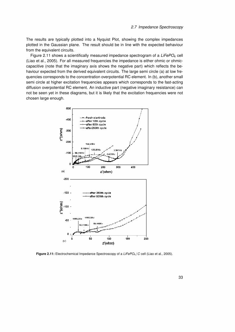
The results are typically plotted into a Nyquist Plot, showing the complex impedancesplotted in the Gaussian plane. The result should be in line with the expected behaviourfrom the equivalent circuits.
Figure 2.11 shows a scientifically measured impedance spectrogram of a LiFePO4 cell(Liao et al., 2005). For all measured frequencies the impedance is either ohmic or ohmic-capacitive (note that the imaginary axis shows the negative part) which reflects the be-haviour expected from the derived equivalent circuits. The large semi circle (a) at low fre-quencies corresponds to the concentration overpotential RC element. In (b), another smallsemi circle at higher excitation frequencies appears which corresponds to the fast-actingdiffusion overpotential RC element. An inductive part (negative imaginary resistance) cannot be seen yet in these diagrams, but it is likely that the excitation frequencies were notchosen large enough.
heat-treatment.25 This is important for the preparation of high-performance lithium-ion phosphate cathode materials.
Figure 5 illustrates the rapid charge–discharge cyclic perfor-mance of the LiFePO4/C cathode. The cell was charged with2 C c.c. + 4.2 V c.v. mode and discharged at 2 C rate to 2.0 V atroom temperature. It was clearly observed that the discharge capac-
ity increased gradually in the initial cycling stage. After 30 cycles,the steady discharge capacities were achieved at about127–131 mAh/g. The stable performance lasted for 300 cycles, thenthe discharge capacity dropped gradually to 93 mAh/g at the 500thcycle. After a following cycle of 0.1 C rate charge and discharge, thecell capacity recovered to 110 mAh/g. However, in the following 2C rate cycling the decrease trend continued. The discharge capacitydropped to 65 mAh/g at the 800th cycle.
To further understand the material behavior, EIS was applied.Figure 6 shows the Nyquist plots of the Li ! LiFePO4/C cell in thecompletely discharged state as a function of cycle number. It can beseen that the Nyquist plots for the fresh cell and the cell after tencycles are comprised of a depressed semicircle in high-to-mediumfrequency range and a line inclined at constant angle to the real axisin the frequency range below 4 Hz. The high-frequency intercept atthe x axis corresponds to the ohmic resistance of the cell. The de-pressed semicircle in the higher frequency range is mainly related tothe complex reaction process at the electrolyte /cathode interface,which may include the migration resistance of SEI film formed onthe surface of LiFePO4 particles, the particle-to-particle contact re-sistance, charge-transfer resistance, and corresponding capacitances.The inclined line in the lower frequency range is attributed to theWarburg impedance, which is associated with lithium-ion diffusionthrough the LiFePO4 electrode. It can be seen that the size of thehigher frequency semicircle apparently decreases with the increaseof cycle number. This phenomenon can be explained in the follow-ing way: Once the cell was cycled, the diffusing paths of lithiumions were gradually developed with the permeation of electrolytethrough electrode particles upon cycling. More active reaction siteswere produced and the conductivity of lithium ions was improved in
Table I. Impedance parameters derived using equivalent circuit models for Li ¸ LiFePO4/C cell.
a R!: ohmic resistance R1: resistance parameter for higher frequency semicircle R2: resistance parameter for lower frequency semicircle.b Q1,Q2: CPE; T and P are the constant phase parameters of the equation Z = 1/$T"I*##p% used for fitting the depressed semicircles in the Nyquist plots
!* represents the complex conjugate I = &!1; # is the angular frequency of the ac signal".c P, R, T are the Warburg "W# parameters of the equation Z = R*ctnh"$I*T*#%P#/"I*T*##P used for fitting the low-frequency straight line of the Nyquist
plots.d Calculated using model 1.e Calculated using model 2.
Figure 6. EIS plots of the Li ! LiFePO4/C cell after different cycles in thedischarged state.
Figure 7. Equivalent circuit models used for fitting of the impedance spectraof the Li ! LiFePO4/C cell.
A1971Journal of The Electrochemical Society, 152 !10" A1969-A1973 !2005" A1971
www.esltbd.org address. Redistribution subject to ECS license or copyright; see 130.95.148.111Downloaded on 2013-03-14 to IP
Figure 2.11: Electrochemical Impedance Spectroscopy of a LiFePO4/C cell (Liao et al., 2005).
33
2 Batteries
The simplifications incorporated into the equivalent circuits proposed (replacing the War-burg impedance by only two RC elements) seems justified. It is remarked that batteriesstill are chemical constructions which undergo highly dynamic, non linear responses. TwoEIS plots of the same battery at the same state of charge at the same temperature with thesame range of frequencies but different excitation amplitudes would not provide the sameresults, for example. Another example is the dependancy of the capacity on the dischargecurrent which is discussed next.
2.8 Peukert’s Law
Wolfgang Peukert empirically described a dependancy between the available capacity oflead-acid batteries and the rate at which they are discharged in 1897 (Peukert, 1897). ThePeukert equation is often stated as:
Cp =
I1A
k
t (2.12)
where:
• Cp is the capacity at a 1A-discharge-rate,
• I is the actual discharge current,
• t is the actual time to discharge the battery.
For practical cells, the capacity at a 1A discharge rate is not usually given. It is useful toreformulate the law to a known capacity and discharge rate:
It = C
CIH
k1
(2.13)
where:
• H [h] is the rated discharge time,
• C [Ah] is the rated capacity at that discharge rate,
• I [A] is the actual discharge current,
• k [1] is the Peukert coefficient,
• t [h] is the actual time to discharge the battery
For example, a battery with a Peukert coefficient of k = 1.2 and a rated capacity ofC = 100Ah at a rated discharge time of H = 10h would provide a capacity of only
34
2.9 Definitions and Characteristics
It = 100Ah
100Ah20A · 10h
0.2
= 87Ah. (2.14)
when discharged at I = 20A and thus t = 5h. Peukert’s law is an empirical law which isa mathematical fit of the observation with no physical background. Typical values of k arebetween 1.1 and 1.3 for lead-acid batteries while Lithium batteries achieve values of 1.05and thus closer to the ideal of 1.
It is controversially discussed (Doerffel and Sharkh, 2006) whether Peukert’s equationcan be used to predict the SoC of a Lithium-ion battery if it is notdischarged at a constantcurrent and a constant temperature.
2.9 Definitions and Characteristics
In the context of batteries, it is usual to use a few common definitions and abbreviationswhich are presented next besides typical characteristics.
2.9.1 State of Charge
The State of Charge (SoC) is the percentage of the maximum possible charge that ispresent inside a rechargeable battery (Pop, 2008, p. 3):
SoC =Cavl
Cfull. (2.15)
When a battery is new, the full capacity equals the nominal capacity:
Cfull = Cnom. (2.16)
The SoC also depends on the discharge rate and the temperature.
2.9.2 Degree of Discharge
A valuable measure is the degree of discharge (DoD) [Ah]. Though related to the Stateof Charge, it is given as an absolute measure rather than a relative one. For example, a100Ah battery could be at 0% SoC at a DoD=100Ah when new but reach that SoC alreadyafter DoD=75Ah due to ageing or when discharged at a higher rate than specified, as thedisposable amount of charge depends on the discharge rate according to Peukert’s Lawwhich is discussed in section 2.8. Also, when discharging a battery at a lower rate thanspecified, it is possible that the DoD overtops the nominal capacity Cnom but the initial SoCwould still be 100%.
35
2 Batteries
2.9.3 State of Health
State of Health (SoH) is a ’measure’, typically a number between 0 and 1, that reflectsthe general condition of a battery and its ability to deliver the specified performance incomparison to a fresh battery (Pop, 2008, p. 3). Common numbers SoH calculation al-gorithms rely on are for example the cycle count, which means how often a cell has beencharged/discharged, tracking of the inner impedance (see figure 2.12), tracking of the fullcapacity, numbers of operations outside a safe operational area (SOA) et cetera.S. Cheng et al. / Journal of Alloys and Compounds 293–295 (1999) 814–820 819
Fig. 10. EIS of battery C with voltage decay during the initial stage of cycling.
battery deterioration during cycling. Fig. 10 shows that, 4. Conclusionswith an increase in the number of cycles, R increasessgradually, which leads to a decrease in voltage. The 1. The EIS of a Ni /MH battery consists of a semicircleincrease of R is mainly due to the drying out of the and a sloped straight line. The semicircle reflects thesseparator, and thus results in an increase of the ohmic electrochemical process of the battery, the diameter ofresistance of the battery. This inference is supported by the which indicates the reactive impedance (R ) of thetfollowing test: dead batteries were dissected and immersed electrode reaction. The slope of the straight line isin an electrolyte of 6 M KOH solution. It was discovered related to the diffusion process of the protons in thethat the voltage performance and capacity of the batteries electrode.almost entirely recovered. In Fig. 11, EIS indicates that, 2. During activation, R and R of the battery decreaset swith an increase of cycling, R stays almost constant, while markedly, and both tend to constant values after three tosR increases gradually. In this case the battery performance five cycles.tundergoes a constant decrease of capacity with the voltage 3. There are two main types of battery deterioration. Oneremains essentially unchanged. Hence, the voltage per- is caused by capacity decay, and the other by voltageformance of the battery is related to R , while battery decay. The former is due to the increase of R , while thes tcapacity is related to R . latter is caused by an increase of R .t s
Fig. 11. EIS of battery B with capacity decay during cycling.
Figure 2.12: Electrochemical Impedance Spectrograms of a NiMH cell which suffered early damage due to avoltage decay during the initial stage of cycling (Cheng et al., 1999).
2.9.4 C-Rate
The C-Rate is a useful and commonly used nominal capacity-proportional charge- or dis-charge current and defined as:
IC [A] = C · Cnom[Ah]1h
(2.17)
For example, a Cnom = 100Ah battery has a 0.5C-rate of I0.5 = 50A or a 2C-rate ofI2.0 = 200A, while the discharge times are t0.5 = 2h and t2.0 = 30min, respectively.
2.9.5 Charge- and Discharge Characteristics
Figure 2.13 shows the discharge characteristics of a LiFePO4 cell at different dischargecurrents. Full capacity is only available at low discharge currents. However, cells whichhave been discharged at high rates first can be discharged at low rates to a 100% DoD.
36
2.9 Definitions and CharacteristicsHIGH CAPACITY LFP26650EV ENERGY CELL DATA
Executing Engineering Excellence
Performance may vary depending on application All specifications and operation conditions are subject to change without notice. This data is for evaluation purposes only. No guarantee is intended or implied by this data. Rev. SP-700080-001 / A
1125 American Pacific Drive, Suite C • Henderson, NV 89074 • 702.478.3590 • www.K2battery.com
Figure 2.13: Discharge Curves of a LiFePO4 cell for different discharge currents (Image courtesy of K2Energy).
Noteworthy is the low voltage decay over large parts of the SoC. Discharge curves alsoreveal an internal DC resistance of approximately 20m.
The open circuit voltage underlies a hysteresis (Roscher and Sauer, 2011), whichmeans that the direction of previous current has an effect on the settled open circuit voltage(figure 2.14)
M.A. Roscher, D.U. Sauer / Journal of Power Sources 196 (2011) 331–336 333
Fig. 1. Voltage response on a 20C constant current charge pulse (a) and the preferred battery electric equivalent circuit for voltage reconstruction (b).
frequency of the current excitation.
Ucell(j!) = Icell(j!) ·
Rs +Rp
1 + j!RpCp
+ OCV (1)
The simulated voltage response on the constant current pulse usingthe illustrated equivalent circuit is given in Fig. 1a. By fitting thecomponents Rs, Rp, Cp of the equivalent circuit, the voltage can bereproduced accurately. With the simple RRC-model the maximumdeviation between the modeled and the measured voltage is lessthan 4 mV during the applied 20C pulse. During the current pulsethe OCV changes, due to the changing SOC. The OCV drift leads tothe difference between the measured cell voltage and the voltageof the battery model (where the OCV is held constant) for t > 40 s inFig. 1a.
4.2. OCV model development and parameterization
The gradual complete discharge and subsequent charge cyclesemphasize the pronounced OCV hysteresis of the investigated cells.This is expected since it is known that LiFePO4 [15] and graphite[16] exhibit pronounced OCV hysteresis phenomena. Hence, theOCV after previous charge is higher than the OCV after dischargeat the same SOC value, which is illustrated in Fig. 2. Accord-ingly, two different OCV curves exist, OCVcharge and OCVdischarge,describing the specific OCV characteristics of the investigatedcells.
Both of the curves comprise characteristic OCV plateaus. The gapbetween the two curves depends on the SOC and exhibits local min-ima at SOC = 40% and 85% and local maxima at SOC = 20% and 65%and reaches a maximum value of approximately 60 mV. For OCV
Fig. 2. OCV curves of the LiFePO4-based cells depending on the previous currentdirection, measured after various rest periods at each step.
model development both of the curves (OCVcharge and OCVdischarge)will be considered.
In Fig. 2 the measured OCV values after 1 min, 5 min and 30 minrest time are inserted additionally. These intermediate values indi-cate that the OCV recovers over several minutes and even hoursuntil a steady state is reached. (The OCV changes less than 1 mVfrom 3 h to 8 h rest and hence is assumed to be stable.) Moreover,the voltage decay depends on the SOC. The characteristic plateauscannot be identified clearly after 1 min rest; they rather emergeduring rest. The OCV recovery is depicted in Fig. 3, plotted overSOC, where the differences between the measured OCVs after cer-tain rest durations and the OCV curves after 3 h rest, which areassumed to be almost stable, are given.
The cell voltage recovery over several minutes or hours can-not be reproduced with the simple equivalent circuit model as it isgiven in Fig. 1b, comprising a resistor Rs connected in series witha parallel RC branch (Rp, Cp). The OCV decay effect has to be con-sidered separately. A possible way to incorporate the informationabout the rest time for OCV reproduction is to introduce a recoveryfactor ", which indicates whether the OCV is completely recovered(to its values after 3 h rest) or not. During load the recovery factoris equal to " = 1 and " = 0 if the OCV is in a steady state after 3 h rest.Therefore, the transition from " = 1 to " = 0 during rest periods isassumed to proceed as first order exponential decay, according toEq. (2), with the time constant of the OCV decay #.
"(trest) = exp!trest
#
(2)
The cell voltage values at the beginning (trest " 0) of the distinctrest periods as well as after very long rest periods (trest " #) are
Fig. 3. Voltage recovery during gradual OCV testing for various rest durations plot-ted over SOC, with the OCV after 3 h used as reference.Figure 2.14: OCV curves of LiFePO4-based cells depending on the previous current direction, measured after
various rest periods at each step (Roscher and Sauer, 2011).
2.9.6 Temperature Characteristics
Battery behaviour is strongly dependant on the ambient temperature while - until certainlimits - higher temperatures correlate with better performance. The reason for that is theQ10 temperature coefficient, a measure of the rate of change in a biological or chemicalsystem as a consequence of increasing the temperature by 10°C, which is typically 2-3 in
37
2 Batteries
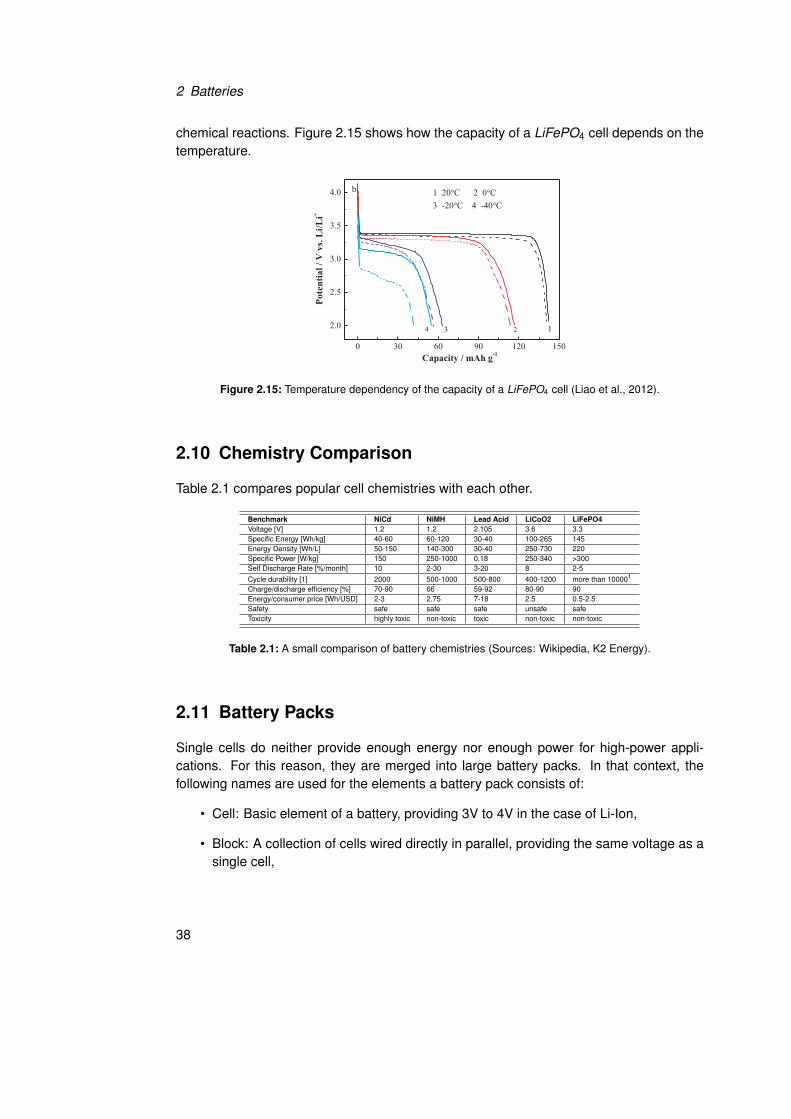
chemical reactions. Figure 2.15 shows how the capacity of a LiFePO4 cell depends on thetemperature.
L. Liao et al. / Electrochimica Acta 60 (2012) 269– 273 271
0.0 0.5 1.0 1.5 2.0 2.5 3.00
8
16
24
32
40
48
56
64 20°
°°
°C 0 C
-20 C -40 C
Cur
rent
den
sity
/ mA
g-1
Time / h
Fig. 3. Profiles of tapering current vs. constant-voltage charging time at 20, 0, !20and !40 "C, respectively.
temperature decreased, the capacity decreased and the electricalpolarization increased, especially at !20 "C, as indicated by thevoltage difference between the charge (increase) and discharge(decrease) plateaus. Charge capacity at 0 "C, !10 "C and !20 "Cwere 138.8 mAh g!1, 134.3 mAh g!1 and 130.2 mAh g!1, separately.The reversible discharge capacity at 0 "C, !10 "C and !20 "C were113.6 mAh g!1, 102.9 mAh g!1 and 58.9 mAh g!1.
Compared with Fig. 2(a) and (b), we can find that no matter thecell is charged at the room temperature or at the low tempera-ture, discharge capacity is slightly affected by charge temperaturein range of !20 to 20 "C.
Furthermore, at !20 "C, all lithium ions can almost be extractedby delivering similar charge capacity as that of at 20 "C. However,the discharge capacity at !20 "C was below 50% discharge capacitydelivered at 20 "C, demonstrating that for a given CV time limit,although the lithium ions can totally extract by using CC/CV modeat low temperature, the lithiation process is still blocked at lowtemperature by exhibiting very low capacity.
Fig. 3 shows the change trends of tapering current during CVcharge period at various temperatures. Cells were charged in CVmodel for 1 h and 3 h after being charged in CC model. The cur-rent decreases quickly and then slowly tends to be stable as theCV time extends to 3 h. It is shown that the lower the temperature,the more the elapsed time before the current tends to be steady,indicating that more time is required for complete delithiation. Forexample, when the temperature is above 0 "C, lithium ion can becompletely extracted with a CV time limit of 1 h, but the temper-ature drops below !20 "C, CV time limit of 3 h or even much moreis needed. Thus, moderately extending CV charging time may bea potential method to ensure lithium ion be completely extractedand be delivering more discharge capacity.
In order to investigate the effect of CV charge time on dis-charge capacity, discharge curves of LiFePO4/Li cell charged byCC/CV model (CV for 1 h and 3 h) under different temperatureswere shown in Fig. 4. Both charge and discharge were car-ried out at the same temperature. Compared with a capacity of138.9 mAh g!1 (20 "C), 113.8 mAh g!1 (0 "C), 56.7 mAh g!1 (!20 "C)and 41.7 mAh g!1 (!40 "C) for CV time of 1 h, LiFePO4 cathode ofthe CV charge time for 3 h delivered reversible discharge capacity of140.5 mAh g!1 (20 "C), 116.5 mAh g!1 (0 "C), 63.4 mAh g!1 (!20 "C)and 54.7 mAh g!1 (!40 "C), the discharge capacities at 20 "C and0 "C were almost unchanged with constant voltage time extended.However, it is worth mentioning that the discharge capacities at!20 "C and !40 "C increased by 11.8% and 31.2%, the low temper-ature capacity retention related to 20 "C increased from 40.8% to
0 30 60 90 120 150
2.0
2.5
3.0
3.5
4.0
Capacit y / mAh g-1
Pote
ntia
l / V
vs.
Li/L
i+
4 3 2
1 20°C 2 0°C3 -20°C 4 -40°C
1
b
Fig. 4. Discharge curves with different constant-voltage charge time at 20, 0, !20and !40 "C, respectively. (Dashed line: 1 h; solid line: 3 h.)
45.6% (!20 "C) and 30.3% to 38.9% (!40 "C), demonstrating thatlowing the temperature, the effect of CV time on discharge capacityincreased obviously. With the temperature decreased, diffusion oflithium ion through electrode materials gets more difficult, [18,19]extend CV time limit can ameliorate the diffusion between thesolid phase and make lithium ion insertion process more smoothly.These further confirm that an extended CV time limit is helpful toimprove the discharge capacity by certain extent at low tempera-ture, especially below !20 "C. Furthermore, it is clear that voltageplateau of CV time for 3 h is slight higher than that of 1 h. We con-firm that extending CV time can compensate overpotential due tothe polarization of concentration difference and electrochemicalpolarization.
Seen from the above discussions, it is seen that an effectivemethod to enhance the low temperature discharge capacity canbe proposed from the charge–discharge regime by extending theCV time.
To understand the origins for this low temperature capacitychange and the effect of temperature on charge/discharge, the EISof full charged and discharged state was measured and analyzed atvarious temperatures in Fig. 5.
The impedance spectrum is generally composed of two partiallyoverlapped semicircles at high frequency and medium frequencyand a straight sloping line at the low frequency end. Such an EISpattern can be fitted by equivalent circuit in Fig. 6 [15]. Where, Rbis bulk resistance reflecting the electric conductivity of the elec-trolyte, separator, and electrode; Rsei and Csei are resistance andcapacitance of the solid-state interface layer formed on surface ofelectrode, which correspond to the semicircle at high frequency; Rctand Cdl are charge-transfer resistance and its related double-layercapacitance between electrode and electrolyte, which correspondto the semicircle at medium frequency; W is Warburg impedancerelated to the lithium ions diffusion in the active material, whichis indicated by a straight sloping line at the low frequency. Thecorresponding values were list as shown in Table 1.
Note that at !40 "C, the impedance spectrum of the low fre-quency shows some noise, it maybe the low frequency limit(0.01 Hz) of the impedance measurement is too high to observeaccurately the diffusion process of lithium ion, similar phenomenonwas found previous reports. [17,20] Therefore, we only investigatethe change of resistance at high frequency and medium frequencydespite that Warburg diffusion is an important factor influencinglow temperature performance [19].
Fig. 7 shows the relations between resistance and tempera-ture at full discharged and charged state. It is observed that theRb and Rsei vary with the temperature in a very similar manner,
Figure 2.15: Temperature dependency of the capacity of a LiFePO4 cell (Liao et al., 2012).
2.10 Chemistry Comparison
Table 2.1 compares popular cell chemistries with each other.
Benchmark NiCd NiMH Lead Acid LiCoO2 LiFePO4Voltage [V] 1.2 1.2 2.105 3.6 3.3Specific Energy [Wh/kg] 40-60 60-120 30-40 100-265 145Energy Density [Wh/L] 50-150 140-300 30-40 250-730 220Specific Power [W/kg] 150 250-1000 0.18 250-340 >300Self Discharge Rate [%/month] 10 2-30 3-20 8 2-5Cycle durability [1] 2000 500-1000 500-800 400-1200 more than 100001
Table 2.1: A small comparison of battery chemistries (Sources: Wikipedia, K2 Energy).
2.11 Battery Packs
Single cells do neither provide enough energy nor enough power for high-power appli-cations. For this reason, they are merged into large battery packs. In that context, thefollowing names are used for the elements a battery pack consists of:
• Cell: Basic element of a battery, providing 3V to 4V in the case of Li-Ion,
• Block: A collection of cells wired directly in parallel, providing the same voltage as asingle cell,
38
2.11 Battery Packs
• Battery: A collection of blocks wired in series to provide a higher voltage,
• Battery Pack: A collection of batteries, arranged in any series or parallel combina-tion.
Picture 2.16 shows an example of a large 25.6V/128Ah LiFePO4 battery consisting of 8blocks à 40 cylindrical cells. Two of these batteries in series (yielding 51.2V/128Ah) formthe traction pack of the Formula SAE car.
Dimension of one battery is 104x208x520mm. The pack can provide a continuous cur-rent of 480A and handle 30s-peaks of up to 1120A at a DC resistance of 4m.
Figure 2.16: A large 25.6V/128Ah LiFePO4 battery consisting of 8 blocks of 40 3.2Ah cells in parallel.
39
3 Battery Management System
A Battery Management System (BMS) is designed to put any of the following tasks intoexecution:
• Monitoring the battery status,
• Protecting the battery,
• Estimating the battery’s state,
• Maximizing the performance of the battery,
• Reporting back to users or external devices.
In order to fulfil these tasks, it must accomplish the following functions:
• Prevent that the voltage of any cell exceeds a certain limit or drops below a certainlimit by disabling the charging current or requesting that it be stopped.
• Avoid cell temperatures that exceed a limit by stopping the battery current directly,requesting that it be stopped, or requesting cooling.
• Prevent the charging or discharging current from exceeding a limit.
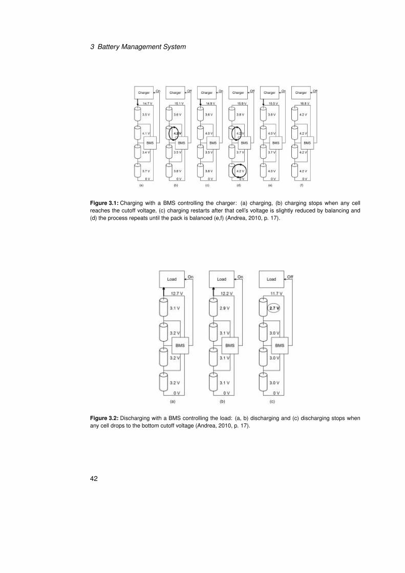
A BMS is essential when charging a Li-Ion battery. As soon as any cell reaches its max-imum charged voltage, the BMS must turn off the charger (see figure 3.1). Overchargingcan provoke a thermal runaway which can cause a fire.
A BMS can also balance the battery in order to maximize its capacity. This can beaccomplished by removing charge from the most charged cell until its voltage is low enoughso that the charger can be applied again and charge the other cells. The process isrepeated until all cells are at the same voltage, fully charged, which means that the packis balanced.
Discharging a Li-Ion battery also requires a BMS. As soon as the voltage in any celldrops to a low cutoff voltage, the load is turned off by the BMS (see figure 3.2) (Andrea,2010, p. 16).
41
3 Battery Management System
wise, a commercially available BMS will get you there much faster for much lessmoney, with fewer resources and a higher likelihood of success. Simply put:
1.3 Li-Ion BMSs 17
Figure 1.16 Charging with a balancing BMS controlling the charger: (a) charging; (b) charging stopswhen any one cell reaches the top cutoff voltage; (c) charging restarts after that cell’s voltage is slightlyreduced by balancing; and (d) the process repeats until (e, f) the pack is balanced.
Figure 1.17 Discharging with a BMS controlling the load: (a, b) discharging; and (c) dischargingstops when any one cell drops to the bottom cutoff voltage.
Figure 3.1: Charging with a BMS controlling the charger: (a) charging, (b) charging stops when any cellreaches the cutoff voltage, (c) charging restarts after that cell’s voltage is slightly reduced by balancing and(d) the process repeats until the pack is balanced (e,f) (Andrea, 2010, p. 17).
wise, a commercially available BMS will get you there much faster for much lessmoney, with fewer resources and a higher likelihood of success. Simply put:
1.3 Li-Ion BMSs 17
Figure 1.16 Charging with a balancing BMS controlling the charger: (a) charging; (b) charging stopswhen any one cell reaches the top cutoff voltage; (c) charging restarts after that cell’s voltage is slightlyreduced by balancing; and (d) the process repeats until (e, f) the pack is balanced.
Figure 1.17 Discharging with a BMS controlling the load: (a, b) discharging; and (c) dischargingstops when any one cell drops to the bottom cutoff voltage.Figure 3.2: Discharging with a BMS controlling the load: (a, b) discharging and (c) discharging stops when
any cell drops to the bottom cutoff voltage (Andrea, 2010, p. 17).
42
3.1 Topologies
3.1 Topologies
How can a battery management system be realized? Three different concepts shall becompared in the next subsections, namely:
• The centralized BMS,
• the modular BMS,
• the Master-Slave-BMS,
• the distributed BMS with control wires and
• the distributed BMS without control wires (using powerline communications).
3.1.1 Centralized BMS
A centralized BMS (figure 3.3) is located in a single assembly, which is connected to thecells via a bundle of wires (N+1 wires for N cells in series). Advantages include:
• Economic reasons: only one printed circuit board (PCB) with one microchip isneeded.
• Maintenance and repair: if a repair is required, it is easier to replace just a singleassembly.
• Accuracy: centralized BMS use the same offsets for all cells.
Disadvantages include:
• Tap wires are referenced to high voltage and a short to the chassis results in a lossof isolation.
• "Spaghetti" problem: Hundreds of wires can run through the high voltage-section,increasing the risk of shorts considerably.
• Adding additional cells is not possible at all if all input ports are used or vice versa,some inputs might stay unused.
• No temperature measurement of each individual cell is possible.
• No voltage measurement is possible during the balancing process, as the drop in IRvoltage across the long tap wire is considerably large.
• Error proneness: tap wires can fit into many inputs.
• Crimp connections are prone to getting loose.
A representative of this topology is Convert The Future’s Flex BMS-481.1
A modular BMS (figure 3.4) is similar to a centralized one, except it is subdivided intomultiple, identical modules, each with its own wirebundle leading to one of the batteries inthe pack. One module takes on the "master" role, commanding the others. Advantagesinclude:
• Manageability: Modules can be placed close to the cells handled by it.
• Scalability: Inserting more cells is feasible by just the addition of more BMS modules.
A disadvantage is mostly the slightly higher cost, as modules have redundant functions.
3.1.3 Master-Slave BMS
In the Master-Slave architecture the functionalities are not equal as opposed to the modu-larized BMS. Slaves are specialized in measuring the voltage of several cells only, report-ing them to a master, which has no voltage measurement function, but can communicate,calculate and control the Slaves and external protectors. Communication between masterand Slaves requires a dedicated communication wire. This architecture is shown in figure3.5. Advantages include:
• Higher specialization: more accurate voltage measurement.
• Lower costs as no unused function needs to be included in either the master or theslaves.
The main disadvantage is that a separate master and slave needs to be designed.A prominent representative of this architecture is eLithion’s Lithiumate BMS.
44
3.1 Topologies
Figure 3.4: A modularized BMS architecture.
Figure 3.5: A Master-Slave BMS architecture.
3.1.4 Distributed BMS
While all the previously discussed topologies had electronics grouped and housed sep-arately from the cells, in a distributed BMS, the electronics are contained on cell boardsdirectly placed on the cells being monitored. There will be N modules for N cells plusone master module controlling the slaves. Communication runs over a dedicated commu-nication wire, typically a daisy-chain connecting all slaves with the master. This solutionrequires 2N voltage measurement wires for N cells as well as N communication wires.
Advantages include:
45
3 Battery Management System
• Temperature measurement of each cell is easy, as the PCB is placed right on top ofthe cells.
• Replacing damaged boards or cells requires detaching of only one module with twowires instead of all N+1 wires needing to be taken off when a centralized BMS fails.
• Better noise immunity due to shorter connection wires allow for more accurate volt-age measurements.
• Specialization allows cheap slaves.
Disadvantages include:
• Higher costs compared to a centralized solution due to the need of N-1 additionalprinted circuit boards plus electronics, as well as 2N+1 more wires.
• Replacement of damaged modules can also be more difficult, as cell modules areinside the battery pack, which is sealed, when its voltage exceeds 40V.
A representative of this architecture is EVpower’s ZEVA-BMS2, which is a very minimal-istic BMS. They use an analogous detection of overvoltage and a 1W passive balancingresistor on each cell, no microcontroller on the slaves and a daisy-chain where every slavecan be closed (everything is okay) or open (in case of a failure). The master can thendetect whether the control line is grounded or tri-state.
Figure 3.7: A real-world distributed BMS setup. Image courtesy of GK Anlagetechnik.
3.1.5 Distributed BMS without communication wires
A distributed BMS without communication wires is the kind of BMS we are currently build-ing. While the cell boards in a distributed system could theoretically even be integratedinto the battery itself, as the only connections are the battery poles, the need for com-munication wires between the cells still exists. If it were possible to use the powerline asa communication medium, this would no longer be a hurdle. This thesis deals with thequestion, whether and to what extent it is possible to replace these wires by powerlinecommunication and to create self-controlling, inherently safe cells, which is achieved bythe master’s ability to switch the load and the charger on and off. The topology is shown infigure 3.8.
3.1.6 Comparison
Although a centralized BMS seems to be the most logical and straightforward approach,coming at the lowest possible costs, its severe disadvantages make the use of a Master-Slave topology or a distributed topology preferable. Not only are these architectures moreversatile, they also come at lower maintenance costs and maximum measurement preci-sion without the need for "spaghetti wiring". Their main disadvantage, the expense, canstill be kept low by using specialized electronics.
47
3 Battery Management System
Figure 3.8: A distributed battery management system without the need for extra wiring since communicationbetween master and slaves is established over the powerline enables the manufacturing of intelligent cells,able to report their state to an external master and receive commands, for example to balance themselves.
3.2 Measurement
3.2.1 Voltage
Measuring the voltage in each cell is crucial for ensuring operation within the safe operat-ing area, and beyond that also essential for further determination of inner cell parameters.Whereas, in the easiest case, the cell voltage could be compared to fixed limits to preventunderdischarging and overcharging, collecting further internal parameters about the bat-tery’s state requires a more precise digital representation. The accuracy is determined bythe assignment:
• Simple detection of the event of a fully charged or discharged cell requires an accu-racy of no more than 100mV, since the OCV vs. SoC curve is very exact at the topand bottom ends.
• Top balancing a battery during the charging process demands an accuracy of 50mV.
• Accurate estimation of a cell’s SoC from its OCV requires an accuracy of 10mV orbetter in order to obtain SoC estimation errors < 10%.
• Accurate estimation of a cell’s SoC from its OCV in the central plateau of the OCVversus SoC curve (20% to 80% SoC) requires an accuracy of 1mV or better. This isa requirement to estimate the SoC with no knowledge of its previous history.
48
3.2 Measurement
Resolution [bit] Accuracy [mV]6 62.58 15.6
10 3.912 1.014 0.2
Table 3.1: Required ADC resolution to achieve a certain measurement accuracy with a maximum voltage of4V.
• To accurately estimate a cell’s internal parameters without an additional amplifier,the accuracy must definitely be below 1mV, the more the better.
The accuracy requirements at a maximum voltage of 4V translates into resolution de-mands of the ADC, as shown in table 3.1.
3.2.2 Current
Knowledge of the battery current is necessary for the following tasks
• for Coulomb-counting fuel gauges,
• to ensure the operation within the safe operation area and
• to enable the slaves to measure the IR compensated open circuit voltage.
High currents can be measured mainly by using
• a current shunt, a small-valued, high-power and high-precision resistor (typically50m or less) or
• a Hall effect current sensor
where Hall effect sensors have the following advantages
• a dissipated power of almost zero
• an inherent insulation from the pack current and
• the potential to measure the current without touching the high voltage.
The main disadvantage of Hall effect sensors is an offset at zero current, which is depen-dant on the temperature in addition. This could create a faultily measured SoC if basedon coulomb-counting. However, Hall effect sensors are used in commercial BMS. A repre-sentative example is eLithion’s Lithiumate Lite BMS. Current shunts, in contrast, have
49
3 Battery Management System
• no offset at zero current,
• no insulation from the pack,
• a slightly variable resistance in response to temperature changes,
• introduction of quite significant energy losses (e.g. 100W at 100A/10m).
Coulomb-counting demands for very high-resolution ADC because standby currents occurat levels as low as several mA. Driving currents on the other hand can reach up to 1000A.Maxim’s DS2740 Coulomb Counter features a 15-bit for currents of ±5.12A using a 10mshunt, TI’s BQ34Z100 fuel gauge uses a 15-bit ADC as well, gauges able to measurecurrents up to 9999A have been reported with 18-bit -ADCs.
Figure 3.9: 1200A/50mV (41.6µ) current shunt as sold by dutch company TBS Electronics. Image courtesyof TBS Electronics, .
3.2.3 Temperature
Measuring the ambient temperature of the battery pack is necessary. However, there isno special requirement on the accuracy - a simple thermal switch with two fixed limitsis sufficient. The typical safe temperature operation range of many LiFePO4 cells variesfrom -20 through +60°C. Many microcontrollers come with integrated temperature sensors,which are absolutely sufficient.
3.3 Balancing
Balancing is a very important function of every BMS to keep the amount of charge of eachcell on the same level and thus maximize the available total energy of the pack. The totalpack energy is limited by the block with the lowest charge. To enable the battery pack
to deliver its full energy capacity, all blocks must be able to provide the same amount ofcharge. When blocks are connected in series every block sees the same in- and outgoingcurrent. Therefore, as every chain, it is as strong as its weakest link, which means in thiscase that the maximum amount of charge Cmax which can be taken from or inserted intothe pack consisting of n blocks with the charges Ci , i = 1...n equals
Cmax = min Ci (3.1)
The balancing process is illustrated in figure 3.10.
0
100
Cell1 2 3
usable charge
SOC [%]
(a) unbalanced
0
100
Cell1 2 3
SOC [%]
(b) balancing
0
100
Cell1 2 3
SOC [%]
usable charge
(c) recharging
Figure 3.10: Balancing of cells with different states of charge. (a) Pack capacity is limited to weakest cell. (b)Balancing pack. (c) Full capacity available after recharging balanced pack.
3.3.1 Balancing Currents
What balancing current is needed? 100mA? 1A? 10A? The answer to this question de-pends on the battery size, the application and whether we talk about gross balancing ora newly installed or repaired pack or just maintenance balancing. While a 1A balancingcurrent would balance a 100Ah pack on a rate of 1%/h and might be acceptable, it wouldbe an overkill for a 10Ah pack. Figure 3.11 gives an overview of the time necessary tobalance grossly unbalanced packs of different sizes.
In general, as soon as a pack has been balanced once, balancing only needs to equalizethe different self-discharge rates. A typical self-discharge rate for LiFePO4 batteries is1%/month. Translated into a 100Ah battery, this implies an average self-discharge rate of1.4mA. If another cell has a self-discharge rate of 1.6mA the required balancing currentwill be only 0.2mA, when operated continuously. However, continuous balancing is notvery commonly used and thus, higher balancing currents are more common. It can bestated, though, that a 1%/h balancing current should be sufficient for most applications.
3.3.2 Algorithms
The next question arising is how to determine the amount of charge that needs to beequalized. A few promising algorithms are listed below:
51
3 Battery Management System
• A balance current of 10 mA will not be able to balance a 1,000-Ah packwithin the lifetime of its owner.
• Conversely, a balance current of 10A would be an overkill for a 1-Ah battery,as it will balance it in less than 6 minutes.
Maintenance BalanceIf a battery starts balanced, keeping it in balance is a far easier job than gross bal-ancing. All that is required is to compensate for the variation in leakage in the cells(self discharge). For example, if all the cells have exactly the same leakage, then nobalancing is required. The SOC of all the cells will slowly drop exactly by the sameamount, so the battery will remain in balance
If all the cells have exactly the same leakage, except for one cell whose leakage is1 mA less, then the BMS has to discharge that one cell at an average current of 1 mAto make up for the difference in leakage (either that, or add 1 mA to all the othercells).
In the example above, the average balancing current was 1 mA. If the BMS cando balancing nonstop, then 1 mA is the actual balancing current. However, in manyapplications, the BMS is turned on only part of the time (yet, leakage dischargescells all the time). In such applications, the balance current has to be higher, ininverse proportion to how much time is available for balancing. For example, if theBMS is only able to balance 1 hour every day, the balance current must be 24 mA toachieve an average of 1 mA.
Of course, it is OK if the BMS is capable of a higher balancing current. If so, theBMS can achieve the required balance current by one of two methods:
• Reduce the balancing current down to the required level;• Turn the balancing current on and off with a duty cycle such that, on the aver-
age, the balancing current is down to the required level.
3.2 Management 77
Figure 3.19 Time required to balance a grossly unbalanced pack versus balance current for vari-ous pack sizes.Figure 3.11: Time to balance grossly unbalanced battery packs of different capacities using different balanc-
ing currents (Andrea, 2010, p. 77).
• Voltage based algorithms,
• Final voltage based algorithms and
• SoC history based methods (Andrea, 2010, p. 66 et. seq).
The goal of each is to equalize the charge level of each cell in the pack. Voltage basedalgorithms aim for equalization of cell voltages, since when the voltages are equal, the SoCis equal. Balancing can take place all the time, which is an advantage, as lower balancingcurrents can be used. Problems with the voltage measurement occur at the flat plateau,where the OCV differences are very small, as demonstrated in figure 3.12.
This disadvantage is overcome by the final voltage based algorithm. However, it allowsonly a short amount of time for balancing, namely the time during which the fullest cell is inits 80%-100%-SoC area, requiring large balancing currents, which is a big disadvantage.
The SoC history based method records the SoC at the end of charge without the on-off-procedure of the charger but measures the charging current instead. As soon as anycell voltage Vc,i starts rising quickly, the current is integrated until the last cell reachesthat voltage - or until the charging process stops as the fullest cell has reached 100%.This integrated current is the charge which can be taken off that cell without risking it tofall below the SoC of the lowest cell. The balancing process can continue while idling ordischarging. After a couple of recharging events, the pack is balanced, without the need forvery large balancing currents or precise voltage measurement. All cells except the lowestcan be balanced simultaneously.
52
3.3 Balancing
algorithm is: energy is removed from the cells whose voltage is above a threshold(such as 3.4V for a LiFePO4 cell).
Later we will analyze balancing in the middle or the bottom instead of at thetop; for now let us assume that balancing is always done at the top. (It is not possibleto balance both at the top and at the bottom, because real-world cells have differentcapacities, so they cannot be balanced both at 100% SOC and at 0% SOC.)
The advantage of this method is that it avoids operating in the flat portion of thevoltage versus SOC curve, where voltage cannot be relied on as a measure of SOC,operating instead at the ends, where voltage is strongly affected by the SOC. When aLi-Ion cell is close to being fully charged, its voltage increases rapidly as it is chargedfurther. A change of 100 mV indicates a change in SOC of on the order of 1~3%.So, if all the cells are within 100 mV, their SOC are also within 1~3%. That is whythis balancing method operates in that area.
One problem with the final voltage algorithm is that usually there is very littletime left between the moment the cell voltages are high enough to start using themfor balancing, and the moment that the charging source is removed. For example,an EV that is plugged in only part of the day may have 2 hours for charging, leavingonly 10 minutes for balancing at the end of charge. A solution to this limitation is touse a much stronger balancing current, to make up for the short time available.
Another problem with the final voltage algorithm is that each cell’s terminalvoltage during charging is higher than its OCV due to the IR drop across its resis-tance, and cell-to-cell variations in resistance can easily affect the cell voltage morethan the SOC does. Therefore, this algorithm could also be counterproductive, byresulting in the discharging of cells with the highest resistance instead of the oneswith the highest SOC, and therefore increasing the unbalance.
3.2 Management 67
Figure 3.13 Difference in OCVs of two LiFePO4 cells versus SOC, at various delta SOC levels.
Figure 3.12: Differences in OCVs of two LiFePO4 cells at different SoCs (Andrea, 2010, p. 67).
3.3.3 Top or Bottom balancing
Real battery packs consist of cells whose capacities don’t match exactly. Therefore, onehas to choose between equalizing the cell´s charge at the bottom and not being able tofully charge all except the lowest capacity cell (figure 3.13) or equalizing at the top, and notbeing able to completely discharge all cells except the one which has reached 100% first(figure 3.14).
Figure 3.13: Three bottom-balanced cells of different capacities. (a) Unbalanced, (b) fully charged, (c) empty.
Which balancing method is preferable? Top balancing offers some serious advantagesover bottom balancing for the following reasons:
1. Top balanced batteries can store more energy. Because higher SoC levels comealong with higher cell voltages, the same amount of charge taken at a higher SoClevel will ultimately lead to a larger energy output.
2. Top balancing allows running of high power loads for a longer time. That is due
53
3 Battery Management System
Figure 3.14: Three top-balanced cells of different capacities. (a) Unbalanced, (b) fully charged, (c) empty.
to the typically negligible low cell resistance which increases with falling SoC levelsand can start limiting the maximum current drawable when many cells come closeto being discharged. Since the average SoC is always higher for top balanced cellsthan it is for bottom balanced cells, the average total resistance is lower, too.
3. Due to certain cell chemistries it is necessary to fully charge cells every once in awhile to maintain an internal chemical balance. For these kinds of cells, top balanc-ing is the only considerable method.
4. Top balancing is more accurate if the SoC is derived from the terminal voltage. IRdrops turn out to be lower at lower currents and the charging current is typically lowerthan the discharging current.
5. Top balancing is more forgiving if the BMS is overridden. A Li-Ion cell dies whenunderdischarged and therefore a BMS should be in charge of stopping the dischargewhen any cell is low. However, the electric car user may decide to override the BMS.If the cells are bottom balanced, all cells will start to die while only the weakest cellwill die if they are top balanced.
6. Charging top balanced cells is easy. A CCCV charger can charge top balanced cells.Constant current is used until one cell is full. Taking a battery on and off the chargeris easily feasible when the cells are top balanced. Constant voltage is applied whenthe current is gradually reduced, until all cells are equally charged (figure 3.15).This algorithm, though working well, has one major limitation: Balancing can onlyoccur during a short period of time. As a consequence, this requires large balancingcurrents or long queue times (Andrea, 2010, p. 75 et seq.).
Balancing can be passive (energy is wasted in heat) or active (energy is transferredbetween cells). In the next subsections, a selection of promising techniques of both kindsare presented.
54
3.3 Balancing
Figure 3.15: Final voltage based top balancing algorithm. After one cell is charged up to 100% SoC (a),charging is suspended by the BMS and all cells above 80% charge or more than the lowest one are balancedto 80% SoC (b, d) or until matching the lowest SoC (f), whichever occurs first. Afterwards, the charging isresumed (c, e), until all cells have reached 100% SoC (g).
55
3 Battery Management System
3.3.4 Active Balancing
The basic idea of active balancing is to use external circuits to actively transport energyamong cells in order to balance the cells. Though none of these techniques can be usedin our BMS due to the requirement for no external wiring, active balancing techniques arean interesting and promising approach which is mentioned in this thesis.
In the last years many different active balancing techniques have been proposed. Sortedby energy flow, they can be grouped in three categories:
1. Cell to pack method,
2. pack to cell method and
3. cell to cell method.
The methods can also be categorized by circuit topology. Possible topologies are
1. shunting methods,
2. shuttling methods and
3. energy converter methods.
We first want to have a look at shunting solutions.
3.3.4.1 Shunting
Figure 3.16: Complete shunting while charging. This method requires at least one diode per cell and twoswitches which need to have a resistance significantly lower than the cell itself. This is very hard to achieveespecially with large batteries or at least very expensive.
Shunting techniques aim at bypassing the charging current if a cell is close to be fullycharged. A complete shunting technique requires two switches and a diode per cell. The
56
3.3 Balancing
setup is shown in figure 3.16. As an example, the top most battery has S1 closed andS4 open while being charged and S4 closed and S1 open when full. The diode preventsshort-circuiting the cell. In practical application this approach will only work if the switchresistances are substantially lower than the cell resistances, which is almost impossibleto achieve, especially when it comes to large cells (100Ah) with inner resistances of lessthan 1m. Other than that, the in-series switches (S1, S2, S3) must be able to handle verylarge currents of 1000A and more in case of an EV. These would be heavy duty and veryexpensive contactors. In addition, in case of a failure of the controller, which closes S1 andS4 at the same time, a low-resistance short-circuit will destroy the switches, interruptingthe current of the complete pack. In summary, as this solution is merely an intellectualpastime rather than a practical solution, we want to keep looking for better solutions toactively balance a battery pack.
3.3.4.2 Shuttling
"Charge shuttling cell balancing mechanisms consist of a device that removes charge froma selected cell, stores that charge, and then delivers it to another cell" (Moore and Schnei-der, 2001).
Flying Capacitor There are several representations of charge shuttling schemes, aninteresting one being a ’flying capacitor’, shown in figure 3.17a. In this method, the cellwith the maximum voltage (e.g. B1) is selected to charge the flying capacitor C. Afterwards,B1 is disconnected again and the cell with the minimum charge (e.g. B3) is selected. Thecapacitor then delivers charge Q to B3 based on the differential voltage between B1 andB3:
Q = C(VB1 VB3). (3.2)
The amount of charge which can be stored in a capacitor is already low in general andbecomes problematic especially when all cells are in the flat plateau of the SoC curve andthus the differential voltage is only several millivolts. A 100mV differential voltage and a100uF capacitor assumed, the exchanged charge is 2.78 · 109Ah only. A high switchingfrequency appears to be key to make this approach work. However, it is limited by thelarge RC time constants formed by the flying capacitor’s equivalent series resistance. Theresistance of the switch (even a MOSFET has typically at least a few 100m) and the largecapacitance. For example, a 1000µF capacitor and a 1 resistance result in a time con-stant = 1ms, limiting the switching frequency to only few 100Hz. A large (100Ah) batterypack requires a charge shuttling device with a very large capacitor with extremely largeswitching currents and therefore a significant amount of energy is dissipated as resistiveheat in the switches and capacitor. Although contributing to balancing, this is counter pro-ductive to the idea of active balancing. However, the technique becomes more interestingwhen operated in the high SoC area. This will often be the case in electric vehicles, since
57
3 Battery Management System
they will routinely be either fully charged or empty. The shuttling device can operate whilecharging and discharging.
A variation of that shuttling method could be a flying capacitor for every two battery cells(figure 3.17b), swapping charge from the higher charged cell to the lower charged cell.Each capacitor only needs simple controls to activate the switches.
volts/cell) and trigger the charger to turn off. Cellbalancing is useful to control the higher voltage cells untilthe rest of the cells can catch up. In this way, thecharger is not turned off until the cells simultaneouslyreach the end-of-charge voltage.
END-OF-CHARGE CELL BALANCING METHODS
Typically, cell-balancing methods employed during and atend-of-charging are useful only for electric vehiclepurposes. This is because electric vehicle batteries aregenerally fully charged between each use cycle. Hybridelectric vehicle batteries may or may not be maintainedfully charged, resulting in unpredictable end-of-chargeconditions to enact the balancing mechanism.
Hybrid vehicle batteries also require both high powercharge (regenerative braking) and discharge (launch assistor boost) capabilities. For this reason, their batteries areusually maintained at a SOC that can discharge therequired power but still have enough headroom to acceptthe necessary regenerative power. To fully charge theHEV battery for cell balancing would diminish chargeacceptance capability (regenerative braking).
CHARGE SHUNTING
The charge-shunting cell balancing method selectivelyshunts the charging current around each cell as theybecome fully charged (Figure 1). This method is mostefficiently employed on systems with known charge rates.The shunt resistor R is sized to shunt exactly thecharging current I when the fully charged cell voltage V isreached. If the charging current decreases, resistor R willdischarge the shunted cell. To avoid extremely largepower dissipations due to R, this method is best usedwith stepped-current chargers with a small end-of-chargecurrent.
B1 B2 Bn
Control
R1
S1
RnR2
S2 Sn
I
I1 I2In
Figure 1. Charge Shunting
Disadvantages of the charge shunting method are therequirement for large power dissipating resistors, highcurrent switches, and thermal management requirements.This method is best suited for systems that are chargedoften with small charge currents.
ACTIVE CELL BALANCING METHODS
Active cell balancing methods employ an active charge-shuttling element or voltage or current converters to moveenergy from one cell to another. These devices can beeither analog or digitally controlled. The two majorclassifications of active cell balancing methods are chargeshuttling and energy converting.
CHARGE SHUTTLING
Charge shuttling cell balancing mechanisms consist of adevice that removes charge from a selected cell, storesthat charge, and then delivers it to another cell. There areseveral embodiments of charge shuttling schemes, themost notable being a 'flying capacitor' (Figure 2).
The control electronics close the proper switches tocharge capacitor C across cell B1. Once the capacitor ischarged, the switches are opened. The switches are thenclosed to connect capacitor C across cell B2. Thecapacitor then delivers charge to B2 based on thedifferential of voltage between B1 and B2 (Eq.1).
The capacitor is then connected in the same manneracross B3, B4, ,Bn, B1, The highest charged cells willcharge C and the lowest charged cells will take chargefrom C. In this way, the charge of the most charged cellsare distributed to the least charged cells. The onlyelectronic controls needed for this method is a fixedswitching sequence to open and close the properswitches.
A variation on the 'flying capacitor' method is intelligentlyselect which cells to balance. In this way, the capacitorcan be charged from the highest cell and selectivelydischarged to the lowest cell. This method candramatically reduce the time to charge balance the cells,especially if the highest and lowest charged cells are onthe opposite ends of the pack. Additional controls arenecessary to detect and select the target cells.
22
21 21
21arg BB CVCVeCh ??
(a)
This method requires a large number of switches (n+5)rated at the peak charging current for C. For a idealsystem (no ESR in the capacitor or switching losses) witha very large cell imbalance (Bn = 3.0V, Bm = 4.0V), a flyingcapacitor could balance these cells at an initial rate of1Ahr per hour per 1000uF of capacitance switching at1kHz with an average switch current of 1A. Figuring in thecapacitor ESR and switching losses dramaticallyincreases the system's time constant for charging anddischarging, effectively reducing actual balancing currentby at least an order of magnitude and increasing the peakswitch current. The larger the capacitor used, the longerit will take to transfer a usable charge and the clock ratewill have to be decreased and the peak switch current willincrease. A large (100Ahr) battery pack would require acharge shuttling device with a very large capacitor withextremely large switch currents. A significant amount ofenergy is dissipated as resistive heating in the switchesand capacitor. A large portion of balancing is simplyachieved by dissipating the charge from the highercharged cells up as heat.
Another charge shuttling method shares a 'flyingcapacitor' for every two battery cells (Figure 3). Thecapacitor constantly switches between the two cells,thereby swapping charge from the higher charged cell tothe lower charged cell. Each capacitor only needs simplecontrols to activate the switches.
B2B1
CControl
I
Figure 3. Charge Shuttling Between Two Cells
Several charge shuttling blocks can be cascaded forhigher voltage packs (Figure 4). Because cells B2 .Bn-1
share flying capacitors with their two neighboring cells,charge can travel from one end of the cell string to theother. This method would take a large amount of time totransport charge from high cells to low cells if they are onthe opposite ends of the pack because the charge wouldhave to travel through every cell with time and efficiencypenalties. This method has a packaging advantage: forevery two cells, the control circuitry, power supply andcapacitor can be packaged in a single unit powered fromthe cells they are balancing. Units can be added as cellcount is increased.
B2B1B3
C1
C2
C3
C4
Control Control
Control Control
I1 I3
I2 I4
B4
Figure 4. Charge Shuttling with Several Cells
Charge shuttling techniques are of limited usefulness forHEV applications. Lithium chemistries offer a relativelyflat open cell terminal voltage across a broad range ofSOC from 40%-80% (Figure 5). A cell at a high SOCdoes not have a significantly large ?V from a low SOCcell, unless one of those cells are on a voltage 'knee' over90% SOC or below 20% SOC. HEV batteries operate inthe mid-SOC range, and this is where the cell-to-cellvoltage differentials are the smallest, thus limiting theusefulness of charge shuttling techniques.
Voltage vs. State of Charge
3.2
3.4
3.6
3.8
4
4.2
4.4
0 20 40 60 80 100State of Charge
Vol
tage
Figure 5. Open Cell Voltage of Lithium Polymer Battery
Charge shuttling techniques are useful for EVapplications. Because an EV can be routinely fullycharged, the voltage differential between a fully chargedcell and a lesser-charged cell is greater near the ends ofthe voltage curve (Figure 5). This increases theeffectiveness of the technique.
ENERGY CONVERTERS
Cell balancing utilizing energy conversion devices employinductors or transformers to move energy from a cell orgroup of cells to another cell or group of cells. Two activeenergy converter methods are the switched transformerand the shared transformer.
The switched transformer method shares the sameswitching topology as the flying capacitor method (Figure
(b)
Figure 3.17: Flying capacitor charge shuttling methods for n cells, (a) using one flying capacitor, (b) using n-1flying capacitors (Moore and Schneider, 2001).
Switched Inductor In 2000, K. Nishijima et. al (Nishijima et al., 2000) proposed a dif-ferent charge shuttling method to overcome the low balancing rates of the flying capacitor.It is a pulse-width modulated (PWM) controlled balancing system, shown in figure 3.18. Ituses a complimentary pair of MOSFET transistors acting as counteracting switches whichare periodically opened and closed in a duty cycle proportional to the voltage differencebetween BC1 and BC2. In case the voltage difference is zero, the duty cycle is 50%. IfBC1 has a higher SoC, the duty cycle will be shifted towards a longer closing time of S1.During this time, BC1 drives a current through S1 and L, which makes the coil build upa magnetic field and store energy in it. As the energy of a coil depends on the currentaccording to
E =12
Li2 (3.3)
and since a rapid change of energy and therefore, a rapid change of current through a coilin zero-time would require infinite power, the coil will counteract a current jump by inducinga voltage according to Faraday’s law
VL = ddt
= Ldidt
. (3.4)
This oppositely directed voltage will cause the source potential of Q2 to drop below GNDand create a current over the body diode of S2, charging the battery BC2. Shortly after-wards, S2 is closed, "charging" L1 in the opposite direction, but for a shorter time interval.
58
3.3 Balancing
The process is demonstrated graphically in figure 3.19 for better understanding. To preventa short-circuit across both batteries when both transistors can be conductive for a shorttime during switching, the authors use a very short "dead time" in which both transistorsare definitely open. Only the body diodes of the transistors prevent a massive voltage peakwhen switching.
In theory, this method, acting as a boost converter, is also able to shuttle energy fromthe lower charged cell to the higher charged cell, which is distinct from the flying capacitormethods.
The outstanding performancing in terms of balancing rates can be remarked in figure3.20. The circuitry is able to transfer 325mAh of charge in less than three minutes using aswitching frequency of 100kHz and a 100µH coil.
an induction between multi-windings of the transformer. However, in these circuits, it is necessary to do a complete coupling among windings. And the control current flowing between the cells and the windings is limited in internal resistances of the respective cells and the other components.
In. PRINCIPLE OF P w M CONTROUED BATTERY BALANCING SYSTEM
Fig. 2 shows a circuit to explain the basic principle of the method presented here, where two cells are balanced by means of PWM. The method is the same as that of a technique of DC to DC converter with duty ratio control. In this system, two cells BCl or BC2 are connected to alternately a choke coil L through switches of complimentary pair. Fig 3 shows switching scheme of this system. In these waveforms, the action of soft switching is neglected to simply the explanation. For driving the complimentary pair switch, an oscillator supplies the square wave with 50% duty as shown Fig. 3 (a). Then PWM control is achieved independently in each switch using variable resistances Rcl and Rc2 controlled by a battery management system (BMS). For example, if the voltage V1 of the cell BCl is higher than the voltage V2 of the cell BC2, a variable resistance RCl is increased by BMS. Then the voltage waveform supplied to the gate of the complimentary pair switch, which draws a transient as shown in Fig. 3(b). Therefore, OR t h e of the switch SI and off time of switch S2 being extended as shown in Fig. 3 (cxd), an average current flowed into the cell BC2 is shifted to positive side as shown in Fig. 3 (e). In the same way, if the voltage V2 is higher than the voltage V1, a variable resistance RC2 is increased, an average current flowed into BC1 is shifted to positive side. Finally, if the voltage Vi equals to the voltage V2, both variable resistances are changed into highest resistance, then the complimentary pair switch is made to be off. Therefore, there is no power loss.
In the conventional system as shown in Fig.1 (c), just after the switches turn off, a large surge voltage arises due to energy stored in the leakage inductance of the transformer during the switches on. For protecting the switch against the surge voltage, a snubber is usually necessary. It will cause a loss in the resistance component of the snubber. In the proposed system as shown in Fig. 2, a surge voltage does not occur by making use of soft switching. This technique is easily achieved by setting in short off interval (dead time) during commutation of the complimentary pair switch. In the dead time of the commutation from the switch S1 to the switch S2, the magnetic energy stored in the choke coil is recovered to the cell BC2 through the body diode of the switch S2. At the same time, the surge voltage is reduced. In addition, a charge stored in parasitic capacitance of switch S2 being also recovered to BC2, the voltage of switch S2 is changed to zero. Because the switch S2 is turned on in this interval, the switching loss is reduced. In the same way, surge and switching loss are reduced during the commutation from the switch S2 to the switch S1.
Fig. 4 is an example for realizing a battery balancing system controlled by PWM, where series connection of 5 cells
B C L 7 ......
Cell vobges f BC2 i ......... lV2 : : : _ . : . . I t j $
Fig. 2 Principle of PWM controlled battery balancing system
i (a) Voltage of the oscillator f ;
. . . (b) Gate voltage of switch i
(c) Drain-source voltage of s 1 j . . . . . .
. . . (d) Mi-source voltage of S2 t t
: I .
(e) Current of Choke coil
Fig. 3 Switching scheme in case of V1 V2
0-7803-5692-61001$10.00 (c) 2000 IEEE 518
Figure 3.18: Switched Inductor Shuttling Method. Counteracting switches S1 and S2 charge the coil in dutycycles proportional to the voltage difference of two batteries BC1 and BC2 (Nishijima et al., 2000).
Active Balancing in a Modular DesignLast, this technique is examined towards it’s suitability for a modular design using powerline communicating slave modules. First of all, one would have to use alternating slaveswith and without a coil at the negative side. Then, Slave A coil negative must be connectedto Slave B positive. In this case, one loses the possibility to store the slave module insidethe battery. The DC/DC converter must be able to handle voltage spikes of 2 ·VBAT + 0.7V .In summary, you can replace 2 transistors and two balancing resistors by 2 MOSFETs and1 coil, saving one part, however you will need an additional bypass capacitor for powerlinecommunications, as the coil acts as a low-pass filter, attenuating the HF signal. Gainingthe ability to balance without a 100% loss in heat, we would be sacrificing the capability ofa modular design towards a design of 2 batteries as the minimum entity.
59
3 Battery Management System
Figure 3.19: Switched Inductor Shuttling Principle. (a) VPWM = high, BC1 charges L (Q1 closed, Q2 open).(b) VPWM = low, Q1 opens and Q2 closes. According to the induction law L pulls V3 below GND potential tomaintain the coil current in the moment of switching and by that, it makes the body diode of Q2 conductive,thus using the lower part of the circuit to remain it’s coil current. By that, it charges BC2. Q1’s body dioderemains non-conductive, as V3 < V1. (c) V3 rises after L has sufficiently recovered it’s energy into BC2, andthe transistor Q2, which has GND potential at it’s gate now, becomes conductive, as VGS < 0. BC2 startscharging L in the opposite direction over Q2. (d) Q1 closes and Q2 opens, L forces V3 to rise above V1 untilQ1’s body diode becomes conductive and charges BC1. The duty cycle of the transistor pair’s gate voltagecontrols which battery discharges more in average.
3.3.4.3 Energy Converters
As seen in the previous paragraph, boost converters can accelerate the balancing process.Such devices employ inductors or transformers to move energy from a cell to another oreven a group of cells.
The switched transformer method (figure 3.21a) uses the same switching topology asthe flying capacitor method. However, current I is taken from the entire pack and isswitched into transformer T. The transformer output is rectified through diode D and de-livered into cell Bn, which is determined by the setting of switches S. Electronic controlselects the target cell and sets switches S. This method can rapidly balance low cells. Dis-
60
3.3 Balancing
balancing system is driven by a frequency of 1OOkHz. Fig. 6 (a) (b) shows experimental results of charging characteristics. In this experiment, initial voltages of BC1, BC4 and BC5 are equal to 3.5V as a full discharged condition, and initial voltages of BC2 and BC3 are equal to 4.0V as a half discharged condition. Fig. 7 (a) (b) shows load characteristics. Also in this case, when a test starts, initial voltages of BC2 and BC3 are equal to 4.3V as a full charged condition, and initial voltages of BCI, BC4 and B5 are equal to 4.0V as a half discharged condition. Fig. 7 and 8 shows that the cell’s voltages are completely balanced by the novel balancing circuit proposed here.
v. CONCLUSlON
In the preceding discussions, we have proposed a novel balancing system for improving the battery lifetime and the performance, and verified the usefulness by the experiments on the charging and discharging characteristics. This system consists of same numbers of DC to DC converters as that of the cell, all cell voltages are completely balanced by PWM control. This system is simple construction because all converters are drove by an oscillator, and PWM controls of respective converters are given by a battery management system. Also high efficiency is realized by making use of soft switching. The number of DC to DC converter will be reduced by using time sharing method.
REFERENCES
[l] B. Lindemark, “Individual cell voltage equalizers (IEC) for reliable battery performance”, in Conf. Rec. INTELEC, Kyoto, Japan, 1991, pp. 196-201
T. Shmpo, H. Suzuki, “Development of Battery Management System for Electric Vehicle”, EVS 14, December 15-17, 1997, Orlando, Florida USA. K. Nishijima, H. Sakamoto, K. Harada, “Balanced Charging of Series
Connected Battery Cells”, lNTELEC’98, October 4-8, 1998, San Francisco, California, USA.
K. Nishijima, H. Sakamoto, K. Harada, “A Magnetic Coupled Simple and High Efficient Battery Management System”, INTERMAG, April 9- 13,2000, Toronto, Canada. H. Kahlen, B. Hauck, “Battery Management with a Two Wire Bus for
Single Cell Charging and Measurement”, EVS-13, October 13-16, 1996,
[2]
[3]
[4]
[SI
Osaka, Japan. [6] M. Homung, M. L. N. Wiegman, D. M. Divan, D. W. Novotny,
Battery System “, IEEE Tran. Ind. Applicate, Vo1.35, No.1, Jan I Feb, 1999.
Design Considerations for Charge Equalization of an Electric Vehicle
Figure 3.20: Outstanding performance of Switched Inductor Balancing both during (a) charging and (b) dis-charging. Five 1350mAh Li-Ion batteries, three of them empty and two of them at 50% SoC initially, arebalanced after less than three minutes. (Nishijima et al., 2000).
61
3 Battery Management System6). Current I is taken from the entire pack and is switchedinto transformer T. The transformer output is rectifiedthrough diode D and delivered into cell Bn, which isdetermined by the setting of switches S. Electroniccontrol is required to select the target cell and setswitches S.
Sn+1
B3B2B1 Bn
Control
S1 S2 S3 S4
I
n:1T
D
Figure 6. Swiched Transformer
This method can rapidly balance low cells at the cost ofremoving energy from the entire pack. Disadvantagesinclude high complexity, high parts count in terms ofcontrol, magnetics, and switches, and low efficiency dueto switching losses and magnetics losses.
A shared transformer has a single magnetic core withsecondary taps for each cell (Figure 7). Current I from thecell stack is switched into the transformer primary andinduces currents in each of the secondaries. Thesecondary with the least reactance (due to a low terminalvoltage on Bn) will have the most induced current. In thisway, each cell receives charging current inverselyproportional its relative SOC.
I
T
B3B2B1 Bn
Control
I1 I2 I3 In
Figure 7. Shared Transformer
The only active component in the shared transformer isthe switching transistor for the transformer primary. Noclosed-loop controls are required. The shared transformercan rapidly balance a multicell pack with minimal losses.Disadvantages of this cell balancing method includescomplex magnetics and high parts count due to each
secondary's rectifier. The balancing circuit would have tobe designed for the maximum expected number of cells;additional secondary taps could not be easily added.
Several transformers can be used with the same result bycoupling the primary windings instead of coupling via asingle magnetic core (Figure 8). The benefit of thismethod is each cell can have its own magnetic core, thusallowing additional cells to be added to the string withoutaltering the host controller.
I
B3B2B1 Bn
Control
I1 I2 I3 In
T1 T2 T3 Tn
Figure 8. Multiple Transformer
The shared transformer method is suitable for both EVand HEV applications. If current I1 is designed to besmall (< 100mA/Ahr capacity), the device could operatecontinuously at a higher efficiency than any of the otheractive methods.
PASSIVE CELL BALANCING METHODS
DISSIPATIVE RESISTORS
The dissipative method shunts selected cells with highvalue resistors to remove charge from the highest cellsuntil they match the charge of the lowest cells (Figure 9).This circuit is the simplest and cheapest cell balancingimplementation. If the resistor value is chosen so that I issmall (<10mA/Ahr capacity), the physical resistor sizeand switch rating can be small. A 10mA/Ahr resistorcould balance severely high cells at a rate of 1% per hour.If operated continuously, such a technique could drain theentire battery pack in a few days.
B1 B2 Bn
Control
R1
S1
RnR2
S2 Sn
I
I1 I2In
Figure 9. Dissipative Method
(a)
6). Current I is taken from the entire pack and is switchedinto transformer T. The transformer output is rectifiedthrough diode D and delivered into cell Bn, which isdetermined by the setting of switches S. Electroniccontrol is required to select the target cell and setswitches S.
Sn+1
B3B2B1 Bn
Control
S1 S2 S3 S4
I
n:1T
D
Figure 6. Swiched Transformer
This method can rapidly balance low cells at the cost ofremoving energy from the entire pack. Disadvantagesinclude high complexity, high parts count in terms ofcontrol, magnetics, and switches, and low efficiency dueto switching losses and magnetics losses.
A shared transformer has a single magnetic core withsecondary taps for each cell (Figure 7). Current I from thecell stack is switched into the transformer primary andinduces currents in each of the secondaries. Thesecondary with the least reactance (due to a low terminalvoltage on Bn) will have the most induced current. In thisway, each cell receives charging current inverselyproportional its relative SOC.
I
T
B3B2B1 Bn
Control
I1 I2 I3 In
Figure 7. Shared Transformer
The only active component in the shared transformer isthe switching transistor for the transformer primary. Noclosed-loop controls are required. The shared transformercan rapidly balance a multicell pack with minimal losses.Disadvantages of this cell balancing method includescomplex magnetics and high parts count due to each
secondary's rectifier. The balancing circuit would have tobe designed for the maximum expected number of cells;additional secondary taps could not be easily added.
Several transformers can be used with the same result bycoupling the primary windings instead of coupling via asingle magnetic core (Figure 8). The benefit of thismethod is each cell can have its own magnetic core, thusallowing additional cells to be added to the string withoutaltering the host controller.
I
B3B2B1 Bn
Control
I1 I2 I3 In
T1 T2 T3 Tn
Figure 8. Multiple Transformer
The shared transformer method is suitable for both EVand HEV applications. If current I1 is designed to besmall (< 100mA/Ahr capacity), the device could operatecontinuously at a higher efficiency than any of the otheractive methods.
PASSIVE CELL BALANCING METHODS
DISSIPATIVE RESISTORS
The dissipative method shunts selected cells with highvalue resistors to remove charge from the highest cellsuntil they match the charge of the lowest cells (Figure 9).This circuit is the simplest and cheapest cell balancingimplementation. If the resistor value is chosen so that I issmall (<10mA/Ahr capacity), the physical resistor sizeand switch rating can be small. A 10mA/Ahr resistorcould balance severely high cells at a rate of 1% per hour.If operated continuously, such a technique could drain theentire battery pack in a few days.
B1 B2 Bn
Control
R1
S1
RnR2
S2 Sn
I
I1 I2In
Figure 9. Dissipative Method
(b)
6). Current I is taken from the entire pack and is switchedinto transformer T. The transformer output is rectifiedthrough diode D and delivered into cell Bn, which isdetermined by the setting of switches S. Electroniccontrol is required to select the target cell and setswitches S.
Sn+1
B3B2B1 Bn
Control
S1 S2 S3 S4
I
n:1T
D
Figure 6. Swiched Transformer
This method can rapidly balance low cells at the cost ofremoving energy from the entire pack. Disadvantagesinclude high complexity, high parts count in terms ofcontrol, magnetics, and switches, and low efficiency dueto switching losses and magnetics losses.
A shared transformer has a single magnetic core withsecondary taps for each cell (Figure 7). Current I from thecell stack is switched into the transformer primary andinduces currents in each of the secondaries. Thesecondary with the least reactance (due to a low terminalvoltage on Bn) will have the most induced current. In thisway, each cell receives charging current inverselyproportional its relative SOC.
I
T
B3B2B1 Bn
Control
I1 I2 I3 In
Figure 7. Shared Transformer
The only active component in the shared transformer isthe switching transistor for the transformer primary. Noclosed-loop controls are required. The shared transformercan rapidly balance a multicell pack with minimal losses.Disadvantages of this cell balancing method includescomplex magnetics and high parts count due to each
secondary's rectifier. The balancing circuit would have tobe designed for the maximum expected number of cells;additional secondary taps could not be easily added.
Several transformers can be used with the same result bycoupling the primary windings instead of coupling via asingle magnetic core (Figure 8). The benefit of thismethod is each cell can have its own magnetic core, thusallowing additional cells to be added to the string withoutaltering the host controller.
I
B3B2B1 Bn
Control
I1 I2 I3 In
T1 T2 T3 Tn
Figure 8. Multiple Transformer
The shared transformer method is suitable for both EVand HEV applications. If current I1 is designed to besmall (< 100mA/Ahr capacity), the device could operatecontinuously at a higher efficiency than any of the otheractive methods.
PASSIVE CELL BALANCING METHODS
DISSIPATIVE RESISTORS
The dissipative method shunts selected cells with highvalue resistors to remove charge from the highest cellsuntil they match the charge of the lowest cells (Figure 9).This circuit is the simplest and cheapest cell balancingimplementation. If the resistor value is chosen so that I issmall (<10mA/Ahr capacity), the physical resistor sizeand switch rating can be small. A 10mA/Ahr resistorcould balance severely high cells at a rate of 1% per hour.If operated continuously, such a technique could drain theentire battery pack in a few days.
B1 B2 Bn
Control
R1
S1
RnR2
S2 Sn
I
I1 I2In
Figure 9. Dissipative Method
(c)
Figure 3.21: Energy Converters used for active balancing. (a) Switched Transformer, (b) Shared Transformer,(c) Multiple Transformer (Moore and Schneider, 2001).
62
3.3 Balancing
advantages include "high complexity, high parts count in terms of control, magnetics, andswitches, and low efficiency due to switching losses and magnetics losses" (Moore andSchneider, 2001).
A shared transformer is built up by a single magnetic core with secondary taps for eachcell (figure 3.21b). Current I from the pack is switched into the transformer and inducescurrents in each of the secondaries. The secondary with the least reactance (due to a lowterminal voltage on Bn) will have the most induced current. This way, each cell receivescharging current inversely proportional to its relative SoC. The shared transformer can"rapidly balance a multicell pack with minimal losses" (Moore and Schneider, 2001). Noclosed-loop controls are required. Disadvantages are complex magnetics, a high partscount due to each secondary’s rectifier and the balancing circuit being designed specificallyfor the given battery pack. Additional taps can not be added easily.
Using several transfomers can overcome this issue with the same result. Instead ofcoupling via a single magnetic core, the primary windings are coupled. This allows eachcell to have its own magnetic core. Furthermore, this architecture is scalable and allowsadding additional cells at a later time (Fig. 3.21c).
The shared transformer method is suitable for EV applications. If current I is designedto be small (< 100mA/Ah capacity), the device could operate "continuously at a higherefficiency than any of the other active methods" (Moore and Schneider, 2001).
3.3.5 Passive Balancing
6). Current I is taken from the entire pack and is switchedinto transformer T. The transformer output is rectifiedthrough diode D and delivered into cell Bn, which isdetermined by the setting of switches S. Electroniccontrol is required to select the target cell and setswitches S.
Sn+1
B3B2B1 Bn
Control
S1 S2 S3 S4
I
n:1T
D
Figure 6. Swiched Transformer
This method can rapidly balance low cells at the cost ofremoving energy from the entire pack. Disadvantagesinclude high complexity, high parts count in terms ofcontrol, magnetics, and switches, and low efficiency dueto switching losses and magnetics losses.
A shared transformer has a single magnetic core withsecondary taps for each cell (Figure 7). Current I from thecell stack is switched into the transformer primary andinduces currents in each of the secondaries. Thesecondary with the least reactance (due to a low terminalvoltage on Bn) will have the most induced current. In thisway, each cell receives charging current inverselyproportional its relative SOC.
I
T
B3B2B1 Bn
Control
I1 I2 I3 In
Figure 7. Shared Transformer
The only active component in the shared transformer isthe switching transistor for the transformer primary. Noclosed-loop controls are required. The shared transformercan rapidly balance a multicell pack with minimal losses.Disadvantages of this cell balancing method includescomplex magnetics and high parts count due to each
secondary's rectifier. The balancing circuit would have tobe designed for the maximum expected number of cells;additional secondary taps could not be easily added.
Several transformers can be used with the same result bycoupling the primary windings instead of coupling via asingle magnetic core (Figure 8). The benefit of thismethod is each cell can have its own magnetic core, thusallowing additional cells to be added to the string withoutaltering the host controller.
I
B3B2B1 Bn
Control
I1 I2 I3 In
T1 T2 T3 Tn
Figure 8. Multiple Transformer
The shared transformer method is suitable for both EVand HEV applications. If current I1 is designed to besmall (< 100mA/Ahr capacity), the device could operatecontinuously at a higher efficiency than any of the otheractive methods.
PASSIVE CELL BALANCING METHODS
DISSIPATIVE RESISTORS
The dissipative method shunts selected cells with highvalue resistors to remove charge from the highest cellsuntil they match the charge of the lowest cells (Figure 9).This circuit is the simplest and cheapest cell balancingimplementation. If the resistor value is chosen so that I issmall (<10mA/Ahr capacity), the physical resistor sizeand switch rating can be small. A 10mA/Ahr resistorcould balance severely high cells at a rate of 1% per hour.If operated continuously, such a technique could drain theentire battery pack in a few days.
B1 B2 Bn
Control
R1
S1
RnR2
S2 Sn
I
I1 I2In
Figure 9. Dissipative MethodFigure 3.22: Passive cell balancing using dissipative resistors (Moore and Schneider, 2001).
Passive balancing techniques remove charge from the highest cells until they match thecharge of the lowest cells. This is, in the easiest case, done by dissipative resistors whichare switched by transistors operated in their active region (see figure 3.22). Although itdoes not seem to be a solution as elegant as the active balancing, since energy is wastedin heat, there are a lot of reasons why this technique has become the favorite of most BMS,among them:
63
3 Battery Management System
1. Simple design.
2. Cheap parts.
3. Easy installation: no inter-cell circuitry needed.
4. Easy scalability.
Additionally, recent improvements in battery manufacturing processes have greatly min-imized unbalances due to limiting different self discharge rates to a minimum level. Batterypacks need to be gross balanced only after having assembled them for the very first time.After that, the balancing circuits only need to equalize tiny differences in different self-discharge rates, which are typically only a few Milliamperes in practical cells. 3
Especially due to the constraint of having no inter-cell circuitry in our project, we rely onthis solution, and design both a Bang-Bang- and a P-Balancing circuitry with adjustablebalancing currents in section 4.10.
3.4 Evaluation
From the measured data, a calculation or estimation of certain parameters relating to thestate of the pack may be executed by the BMS. They include
• State of Charge (SoC) and Depth of Discharge (DoD)
• Resistance and inner parameters
• Capacity and
• State of Health (SoH).
This information is not crucial for the protection of the pack, but for the convenience ofthe user who may be informed prior to failure, when a cell needs to be replaced or the packneeds attention.
3.4.1 State of Charge and Depth of Discharge
One thing a user is typically interested in is the battery’s state of charge to estimate howmuch longer the battery will power their device. The flat plateaus of the SoC vs. voltagecurves of lithium batteries however make fuel gauging an "inexact science" at best and a"wild guessing game" at worst (Andrea, 2010, p. 89). Almost every big chip manufactureroffers a variety of so called "fuel gauge" ICs and this subsection is dedicated to demystifytheir functional principle and even to coming up with a more advanced approach. While a
3Source: Rob Mason, Founder and CEO of Electric Vehicle conversions company EVworks.
lead-acid battery’s SoC can be determined by measuring the density of the electrolyte andNiCd and NiMH batteries offer steep enough SoC vs. voltage curves, a Lithium battery’sSoC cannot be measured directly. However, there are multiple possibilities to estimate theSoC. Among them:
• Voltage translation,
• current integration ("Coulomb counting") and
• inner parameter translation.
3.4.1.1 Voltage Translation
State of Charge estimation by voltage translation seems easy, but is rather complicated.Figure 3.23 shows a real recorded voltage translation function of a LiFePO4 cell. A 12-bitADC with an accuracy of 1mV was used to obtain these results.
Figure 3.23: Voltage translation function obtained by a 12-bit ADC on a real LiFePO4 cell.
How serious a voltage measurement error translates into a SoC estimation error isshown in figure 3.24.
Not only will
• Low-resolution ADCs
65
3 Battery Management System
2.5 2.6 2.7 2.8 2.9 3 3.1 3.2 3.30
5
10
15
20
25
30
35
40
OCV [V]
SOC
Est
imat
ion
Erro
r [%
]
8mV
2mV
1mV
4mV
Figure 3.24: Unprecise voltage measurements lead to untolerably high SoC estimation errors. Shown areSoC estimation errors for different voltage measurement accuracies.
• variances between two different ADCs
• measurement noise and
• unprecise voltage dividers
limit the achievable accuracy massively. Variations on the cell chemistry can even shift theOCV by up to 100mV within the same LiFePO4 technology.
All these limitations make an uncalibrated voltage translation the guessing game men-tioned before. The BMS must at least learn the voltage transfer function for one cycle, butit is common to use voltage translation only outside the flat plateau.
3.4.1.2 Current Integration
A method widely spread is current integration or "coulomb counting". A very small-valued"shunt" resistor (typically below 10m) is connected in series with the battery and the load.The voltage across it is proportional to the current in- or outgoing and the integration of thecurrent is the charge taken out or put into the pack. Disadvantages include
• Cell leakage is not registered and
66
3.4 Evaluation
• offset in the measurement will result in a SoC drift.
A calibration of voltage translation at low and high SoC and coulomb counting at the flatplateau results in very good outcome.
3.4.1.3 Inner Parameters
An additional possibility to estimate the SoC without coulomb integration can be the eval-uation of inner cell parameters. The feasibility will be conducted in section 3.4.3.
3.4.2 Capacity
Measuring the actual available capacity Cavl of a pack is required for a more accurate SoCestimation. A decrease can be used to deduct a decreased State of Health. Required formeasuring the capacity is a coulomb counter and as it is possible to determine the capacityboth by charging from 0% to 100% or discharging from 100% to 0%, it is preferable to doso while discharging because in electric vehicles, discharging typically happens quickerthan charging and thus, the non-IR-compensated dispensable charge could be limited dueto previously mentioned Peukert’s law.
3.4.3 Resistance and Inner Parameters
The most sophisticated approach to gain knowledge about the battery is obtaining innerparameters and gaining further information tracking them. Inner parameters we are inter-ested in, as shown in figure 2.9c, are:
• The ohmic resistance R,
• the diffusion overpotential parameters CD and RD and
• the concentration overpotential parameters CC and RC .
Together, those parameters form the inner resistance
Z = R +RD
1 + j!RDCD+
RC
1 + j!RCCC. (3.5)
The reverse evaluation can help with a better SoC determination, and tracking of theseparameters can help improving the State of Health measurement.
3.4.4 State of Health
State of Health (SoH) is a ’measure’ that reflects the general condition of a battery and itsability to deliver the specified performance in comparison to a fresh battery (Pop, 2008, p.3).
67
3 Battery Management System
The SoH indication may involve for example cycle-counting. In the simplest case thenumber of full charge and discharge cycles can be counted and the SoH can be calculatedbased of a stored maximum capacity function. For users do not always wait until a batteryreaches an empty or full state the system should therefore take into account SoC levelsother than empty and full. Other than that, different types of batteries and different typesof user behaviour can cause problems. Due to this spread, the SoH evolution will bedifferent for each user and application, and will consequently be rather unpredictable. Itis not possible to deal with such unpredictable behaviour with a simple charge/dischargecycles counting implementation. An adaptive system must therefore be used to ensure anaccurate SoC indication when the battery ages. Examples of adaptive algorithms benefitfrom
• Neural networks (Gérard et al., 1997), (Grewal and Grant, Oct.),
• Kalman filters (Plett, 2004) or
• Fuzzy logic (Salkind et al., 1999).
The state of health determination
• is specific for a chemistry, a type of cell, and a manufacturer
• requires a specifically fitted model derived from empirical observations and
• requires training.
Implementing, training and testing these models for specific applications and batteries isa huge task which requires expensive lab equipment, a variety of fresh batteries, pro-grammable loads, high precision data loggers, typically 2000 charges and discharges percell and further on. This thesis focuses on providing the hard- and firmware required to per-form measurements which can then be used to train a SoH-estimation model. Ultimately,the state of health can then be used to display the remaining run-time of the battery to theuser.
68
4 Experimental Platform
This chapter deals with the design of the experimental platform needed to meet the re-search goals stated in the introduction. In detail, a slave module, capable of
• measuring cell voltage,
• measuring cell impedance,
• calculating state of charge,
• calculating state of health,
• communicating with a host PC via RS232,
• communicating with other slaves via power line and
• being powered by the battery it is connected to only
with special focus on
• a small size (max. 60x75mm) to fit a standard sized 90Ah battery,
• a low price to minimize cost of the system consisting of multiple slaves and
• a low current consumption to minimize battery drain
is designed (see figure 4.1).
69
4 Experimental Platform
Figure 4.1: Experimental Verification Platform.
70
4.1 Architecture
4.1 Architecture
First of all, an overview on the experimental verification platform we designed is given.Figure 4.2 shows a block diagram of the platform designed and details are discussed inthe subsequent sections.
Figure 4.2: Architecture of the experimental verification platform and its interface to a PC.
4.2 Microcontroller
The microcontroller is the central unit of the slave. It communicates with the PC, executestasks automatically, for example monitoring cell voltage and balancing, and tasks speciallyrequested, like measuring impedance. Further, it is able to monitor data over a periodof time and send it back to the PC when requested. The powerline communication IC iscontrolled by the microcontroller as well. There is definitely no shortage of microcontrollers.While functionalities between different manufacturers are alike, Atmel’s microcontrollersstand out by offering very short execution times. Most operations are computed in onesingle clock cycle which helps operating them at the lowest possible clock frequency andthus, save energy. Atmel offers the very user-friendly, Visual Studio based IntegratedDevelopment Environment Atmel Studio and uses only one pin for programming by using
71
4 Experimental Platform
the reset signal as a clock signal during programming. The integrated on-chip debuggingplatform helps inspect variables and registers at runtime.
With no real constraints regarding speed and our project being far from utilising all it’splenty of features, the choice would usually have been the cheapest ATmega16 chip.Due to the need for a 12-bit Analog/Digital Converter (ADC) and the need for two Uni-versal Asynchronous Receivers/Transmitters (UART) , one for PC communication andone for communication with the PLC Integrated Circuit (IC) , the more advanced modelATxmega16D4 is chosen in it’s minimum configuration with 16kB Flash memory and 4kBboot section. Some key features contain1:
• Operation voltage ranging from ultra-low 1.6V to 3.6V,
• Operation frequencies of up to 32MHz,
• Ultra-low power consumption of 960µA active and 240µA idle at 2MHz clock fre-quency,
• One 12-channel, 12-bit, 200ksps ADC (Successive Approximation Result (SAR)),
• One 12-channel, 12-bit 200ksps DAC,
• Two Hardware UARTs,
• 16-bit real time counter,
• On-chip debugging interface,
• Sleep functionalities,
• Watchdog timer.
4.3 DC/DC Converter
We use Linear Technology’s LTC3240-3.3 DC/DC Converter which is both a step up andstep down charge pump, providing a stable output of 3.3V at up to 150mA. Featuring alow quiescent current of only 65µA, a shutdown current of below 1µA, high conversionefficiencies and a small package, it suits our demands very well. Important characteristicsare illustrated in figure 4.3.
! Step-Up/Step-Down Charge Pumps Generate Fixed 3.3V or 2.5V Outputs
! VIN Range: 1.8V to 5.5V! Output Current up to 150mA! Automatic Mode Switching! Constant Frequency (1.2MHz) Operation in
Step-Up Mode! Low Dropout Regulator Operation in
Step-Down Mode! Low No-Load Quiescent Current: IQ = 65µA! Built-In Soft-Start Reduces Inrush Current! Shutdown Disconnects Load from Input! Shutdown Current < 1µA! Short-Circuit/Thermal Protection! Available in a 6-Lead (2mm ! 2mm) DFN Package
3.3V/2.5V Step-Up/Step-Down Charge Pump
DC/DC Converter
The LTC®3240-3.3/LTC3240-2.5 are step-up/step-down charge pump DC/DC converters that produce a fi xed regulated output voltage of 3.3V or 2.5V over a wide input voltage range (1.8V to 5.5V).
With input voltages greater than the regulated output voltage the LTC3240 operates as a low dropout regulator. Once the input voltage drops within 100mV of the regulated output voltage the part automatically switches to step-up mode. In step-up mode the LTC3240 operates as a constant frequency (1.2MHz) doubling charge pump.
The LTC3240-3.3/LTC3240-2.5 feature low no load operat-ing current (65µA typical) and ultralow operating current in shutdown (<1µA). Built-in soft-start circuitry prevents excessive inrush current during start-up. Thermal shut-down and current-limit circuitry allow the parts to survive a continuous short-circuit from VOUT to GND.
The LTC3240-3.3/LTC3240-2.5 require only three tiny external ceramic capacitors for an ultrasmall application footprint. The LTC3240-3.3/LTC3240-2.5 are available in a 6-pin (2mm ! 2mm) DFN package.
! 2 AA to 2.5V! 2-3 AA/Li-Ion to 3.3V! Low Power Supplies for Cameras, I/O Supplies,
Audio, PC Cards, Misc. Logic, etc., in a Wide Variety of Handheld Products
Output Voltage vs Input Voltage (Full Range)
APPLICATIO SU
FEATURES DESCRIPTIO
U
TYPICAL APPLICATIO
U
OFF ON
VIN
GND
SHDN
VOUTC– C+
LTC3240-3.31µF 4.7µF
1µF
3.3VIOUT = 150mA2.7V TO 4.5V
3240 TA01a
Li-Ion OR3-CELL NiMH
, LT, LTC and LTM are registered trademarks of Linear Technology Corporation.All other trademarks are the property of their respective owners.Protected by U.S. Patents including 6411531.
Li-Ion to 3.3V at Up to 150mA
INPUT VOLTAGE (V)1.7
OUTP
UT V
OLTA
GE (V
)
3.30
3.40
5.7
3240 TA01b
3.20
3.102.7 3.7 4.72.2 3.2 4.2 5.2
3.50
3.25
3.35
3.15
3.45IOUT = 30mA
(a)
LTC3240-3.3/LTC3240-2.5
43240fb
No-Load Input Current vs Supply Voltage (LTC3240-3.3)
Mode Switch Threshold vs Load Current (LTC3240-3.3)
Effective Open-Loop Resistance vs Temperature (LTC3240-3.3)
TEMPERATURE (°C)–40
EFFE
CTIV
E OP
EN-L
OOP
RESI
STAN
CE (!
)
8
9
10
60
3240 G07
7
6
5–15 10 35 85
VIN = 1.8VVOUT = 3V
SUPPLY VOLTAGE (V)1.7
0
NO-L
OAD
INPU
T CU
RREN
T (µ
A)
10
30
40
50
100
70
2.7 3.7 4.2
3240 G08
20
80
90
60
2.2 3.2 4.7 5.2 5.7
No-Load Input Current vs Supply Voltage (LTC3240-2.5)
SUPPLY VOLTAGE (V)1.7
0
NO-L
OAD
INPU
T CU
RREN
T (µ
A)
10
30
40
50
100
70
2.7 3.7 4.2
3240 G09
20
80
90
60
2.2 3.2 4.7 5.2 5.7
ILOAD (mA)0
V IN
(V)
3.60
3.70
160
3240 G10
3.50
3.4040 80 12020 60 100 140
3.80
3.55
3.65
3.45
3.75DOUBLER TOLDO MODE
(VIN RISING)
LDO TODOUBLER MODE
(VIN FALLING)
Mode Switch Threshold vs Load Current (LTC3240-2.5)
ILOAD (mA)0
2.65
V IN
(V)
2.70
2.75
2.80
2.85
40 80 120 160
3240 G11
2.90
2.95
20 60 100 140
DOUBLER TO LDOMODE (VIN RISING)
LDO TO DOUBLERMODE (VIN FALLING)
SUPPLY VOLTAGE (V)1.80
0
EFFI
CIEN
CY (%
)
10
30
40
50
100
70
2.80 3.80 4.30
3240 G12
20
80
90
60
2.30 3.30 4.80 5.30 5.80
ILOAD = 40mA
ILOAD = 1mA
LDO TO DOUBLERMODE (VIN FALLING)
DOUBLER TO LDOMODE (VIN RISING)
VOUT2V/DIV
200µs/DIV 3240 G13VIN = 2.4VRLOAD = 66!
SHDN2V/DIV
VOUT20mV/DIV
AC COUPLED
500ns/DIV 3240 G14VIN = 2.4VILOAD = 100mA
(b)
Figure 4.3: Characteristics of the LTC3240-3.3 DC/DC Converter. (a) Input-Output-Voltage-Behaviour (b) Ef-ficiency based on input voltage. Images courtesy of Linear Technology.
4.4 Powerline Communication Device
At the moment, the only commercially available powerline communication chip optimizedfor battery communication is offered at an Israeli company named Yamar and is calledSIG60. It provides parallel communication on 7 independant Binary Phase Shift Keying(BPSK) modulated carriers at selectable frequencies of either 1.75, 4.50, 5.50, 6.00, 6.50,10.50 or 13.00 MHz. The message to be transmitted can be transferred via a standardserial signal consisting of one start bit (low), followed by 8 data bits and ended with onestop bit (high), at data rates of up to 115.2 kbps (at 10.50 and 13.00 MHz only). Paritycheck or handshaking are not supported. The device only operates at a narrow rangeof supply voltages of 3.0-3.6V and thus, it must rely on a DC/DC converter when batteryvoltages are outside of that range. The supply current is 40mA on idle and 50mA duringtransmission. As this is a value too high for battery applications (it would drain a 3.2Ahbattery in less than 80h), the device can be set into a sleep mode where the current draindrops by three orders of magnitude to only 80µA while still being able to process messageson the powerline.
The device requires a considerably large amount of outer circuitry, which is shown infigure 4.4.
Decoded data from the powerline is output at HDO while data for transmission is ac-cepted serially at HDI, which is being pulled high when not used by R8. Having passedthe in-built multi-phase modem, the BPSK modulated signal is output through port DTxO,band-pass-filtered around the chosen carrier frequency fc by ceramic capacitor F0 and
73
4 Experimental PlatformPreliminary and proprietary Information of YAMAR Electronics Ltd. Subject to change without notice.
• F0 and F1 are ceramic filters • Adjust R1 for maximal output level without distortion on powerline. • C1 and C2 values depend on crystal used. Usually values are between 0pF (NC) to 1.5pF. • Optional 3MHz HPF for very noisy channels, replace C9 with C9a, C11, D8 and L3 • F1 is an optional communication channel
3.1.1 Ceramic Filter Considerations
The SIG60 is designed to operate with one ceramic filter for transmission and reception. However, if switching between two channels is desired, two ceramic filters are required. The minimum allowable bandwidth of the ceramic filters is +/-60 kHz @ 3dB. Narrow bandwidth limits the maximal bit rate. The SIG60 selectable frequencies meet market available ceramic filters. It is important to select the widest bandwidth available. 1.75MHz, 10.5MHz and 13MHz may use discrete filters. Through hole ceramic filters are available from Oscilent. Nominal
* 1.75MZ can operate only at 9.6Kbps ** 10.5MHz and 13.00MHz operates at 115.2Kbps instead of 9.6Kbps.
Figure 4.4: Powerline Communication IC Yamar SIG60 including outer circuitry. Image courtesy of YamarElectronics, Ltd.,
high-pass-filtered by R12 and C7 at a cutoff-frequency of 1.6kHz. After that, it is ampli-fied by the built-in amplifier and output at TXO, where it passes the de-coupling capacitorsC10 and C4 before entering the power line. The Schottky diodes D1 and D2 protect theIC from voltage spikes on the powerline. The decoding of a RX powerline signal worksanalogously. C5 and C6, with a piece of wire in between acting as inductor, works as a lowpass filter for the voltage supply with a double pole at 22.5MHz, 5nH inductance assumed,dropping at a 40dB/dec rate for frequencies higher than the pole.
The modulated high-frequency (HF) signal and the decoded RS232-signal are shown infigure 4.5.
The subsequent sections provide insight into the communication system according toinformation from the patent (Maryanka, 2006) and the datasheet of the SIG60 IC.
4.4.1 Data Transmission
DC power lines are typically considered as "very noisy communication channels with highlevel impulse noises, causing communication errors over a wide range of frequencies. InAddition, parts of the frequencies [...] may be blocked for long periods of time as a resultof Electro Magnetic Interference (EMI) or strong attenuation resulting from inter-symbol
Figure 4.5: High-frequency signals on the powerline. (a) Signal attenuation: High-frequency TX (bottom) andRX (top) signal. (b) Correct decoding: High-frequency RX signal (top) and decoded byte (bottom). The signalattenuation does not depend on the distance very much, but more on capacitances parallel to the load.
interference, fading and standing waves" (Maryanka, 2006). Therefore, data is transmittedvia symbol codes that have a high resistance to random errors. Resistance to errors isachieved by lengthening the symbol transmission period. According to those sources, thedata which can be transmitted at data rates of up to 115.200 bauds per second or (as 2out of 10 bauds are start and stop bits) 92.160 bits per second is translated into symbolswith a symbol duration Ts of a multiple of the carrier cycle duration Tc , that is
Ts = n · Tc , n 2 N. (4.1)
The carrier frequency isfc = n · fs (4.2)
using a symbol rate of
fs =1Ts
(4.3)
with n being the number of phase shifts within one symbol.Each data symbol is a unique pattern of phase shifts, for example "+90°+90°-90°+90°
-90°-90°" can represent a logical ’1’ and "-90°-90°+90°-90°+90°+90°" can be a logical’0’ for a n = 6 configuration, as shown in figure 4.62 The receiver monitors how manyphase shifts can be detected. A channel is considered bad, if more than 1 in 101 detectedsymbols were assigned by m = 5 = n 1 detected phase shifts instead of 6. Then, thechannel usage strategy is adapted, which can be:
1. Change the pattern length n,2This spread spectrum technique is known from Code Division Multiple Access (CDMA), where one bit is
represented by a combination of so-called "chips".
75
4 Experimental Platform
Figure 4.6: BPSK symbols used for transmission. Shown are symbols of the duration of 6 carrier cycles. 5out of 6 phase shifts are detected by the receiver. (Maryanka, 2006)
2. Change the identification criterion, that is the needed number of correctly detectedphase shifts m or
3. Cease use of a channel for communication.
Additionally, error correction codes (ECC) are used by the system, although not revealedin the patent.
Identifications can be:
1. True positive: intended pattern has been recognized correctly by the receiver.
2. False positive ("noise bytes"): Random noise on the channel causes random phaseshifts of the carrier wave. A data error occurs only when noise causes a prolongedshift over most of the symbol period. Random noise is unlikely to do that for manycycles, thus the likelihood of errors decreases as the symbol period increases. Thatis by choosing large numbers of n at the cost of slower signaling.
3. False negative (lost signals). Can be reduced by decreasing the required number ofphase shifts m.
In general, when there are serious consequences of false positive identification errorsand the channel is noisy, the number of phase shifts can be increased from six to eight
76
4.4 Powerline Communication Device
and the number of detected phase shifts is increased from 5 to 6 at the cost of slowersignaling (Maryanka, 2006). In the underlying system, a symbol rate of fs = 636kHz witha symbol duration of TS = 1.57µs, n = 6 phase shifts per symbol at a carrier frequency offc = 3.8MHz are used.
4.4.2 Channels
Selectable channels with their available bitrates are shown in figure 4.7.Preliminary and proprietary Information of YAMAR Electronics Ltd. Subject to change without notice.
When in command mode, the host can configure the device according to the desired operating parameters. The device enters command mode when pin HDC is lowered to “0”. When in command mode, data on the HDI pin is not transmitted to the bus, but is used to configure the SIG60. The command can be written in any of the allowed bit rates. In order to write to a control register, the host sends two bytes. The first byte begins with the address of the register followed by 5(hex). The second byte is the configuration data, as shown in figure 4.1. The bytes should be sent more than 200nSec after lowering HDC.
First Byte Register Address 5(hex) Second Byte Configuration Data Configuration Data
Figure 4.3 shows the pins involved in the writing process:
T3>1/half bit rate
Figure 4.1 - Writing to a Control Register In order to read from a control register, the host sends one byte. The byte should be sent more than 200nSec after lowering HDC. The byte begins with the address of the register followed by ”D”(hex). The SIG60 will then output the content of the register to pin HDO.
Figure 4.2 shows the pins involved in the reading process:
Figure 4.2 - Reading from a Control register
Examples: In order to write xxH to register 0, lower the HDC pin and write 05xxH In order to write yyH to register 1, lower the HDC pin and write 15yyH In order to read from register 0, lower the HDC pin and write 0DH In order to read from register 1, lower the HDC pin and write 1DH
T1
start bit Address stop bit
HDI Read Command:
HDC:
0 1 3 2
HDI
HDC
stop bit
T3
start bit
Address start bit
stop bit
Configuration Data
0 1 3 2 0 1 3 2 4 5 7 6 d a t a start bit
Data
T1
T2
Figure 4.7: Selectable channels with their available transmission speeds.
4.4.3 Arbitration
Since the power line is a shared medium, there must be a medium access control algorithmfor collision detection and resolution to decide which device is allowed to transmit. Thisarbitration algorithm is shown in figure 4.8
77
4 Experimental Platform
Figure 4.8: Signal arbitration algorithm used to handle multiple transmitters over a shared medium (Maryanka,2006).
4.5 Current Measurement
Current must be known for the following reasons, as the impedance measurement requiresknowledge of the actual current. Only voltage based SOC estimation is possible withoutknowledge of the current. But also voltage based SOC estimation methods require knowl-edge of the actual current, as they measure the open circuit voltage only if no current isdrawn and has not been drawn for a time long enough to have the polarization effectssettled. With knowledge of the current and the impedance, it will be possible to derive theSOC by the voltage only even if the current is not zero. In our test setup, the current ismeasured through an external in-series shunt resistor and the differential voltage appliedto the ADC. In a real Battery Management System, it’s the task of the master to measurethe current and transmit this information to the slaves.
4.6 Undervoltage Protection
A cell specific undervoltage protector must be available to prevent the cell from beingdestroyed by underdischarging. For LiFePO4 chemistries, the low voltage cutoff voltage isUmin = 2.0V . For that purpose, the IC LM8364-2.0 is appropriate. It draws a quiescentcurrent of 0.65uA only and pulls the reset lines low of the other ICs on the board in case ofan undervoltage condition, hence preventing them from operating and draining the batteryfurther.
78
4.7 Voltage Measurement
4.7 Voltage Measurement
Analog/Digital Converters have been developed and are available on the market for a verylong time. Due to their popularity they exist in a vast range for almost any application,serving any demands in bandwidth, sampling time and accuracy. Our specific applicationhas the following constraints/requirements:
1. Standby current consumption must be minimal as batteries shall maintain theircharge.
2. Accuracy must be below e 1mV to precisely track the SOC.
3. Offset must be compensated for an offset free SOC determination.
4. Time domain measurements in the low kHz range must be possible.
Or, translated into hardware requirements,
1. both the voltage divider resistors as well as the ADC input resistance must be ashigh as possible,
2. the resolution must be higher or equal than 12bit .
Offset compensation can not be performed with this architecture, the offset can be reducedto a minimum by choosing lower resistance values of the voltage divider:
R2 RADC (4.4)
It is obvious that this will result in a higher standby current i . Moreover, although minimumvalues are typically supplied in ADC datasheets, the exact value of RADC is unknown whichmakes an offset free measurement more difficult. However, we will see later that it ispossible to overcome this issue.
First of all, a schematic diagram of the voltage measurement circuit is shown in figure4.9. R1 and R2 form a voltage divider to match the maximum input voltage of the ADCconverter. Apart from the stochastic errors, introduced by the measurement inaccuracy ofthe ADC itself and inexact values of R1 and R2, the measurement of the true open circuitvoltage VBAT is superposed by the following systematic errors:
• Finite resistance error : ADC current iADC, included in i , creates a voltage drop atbattery inner resistance, leading to VTerm 6= VBat.
• ADC error : Finite but unknown ADC input resistance RADC < 1 results in an errorof VADC,
• Load resistance error : Connected loads iLOAD > 0, which are not always avoidable,decrease VTerm.
79
4 Experimental Platform
Figure 4.9: Voltage measurement setup. R1 and R2 form a voltage divider, RADC represents the finite ADCresistance, RC the connection resistance and RLOAD the load. The battery open circuit voltage, which is subjectof interest, is VBAT .
What can be done to reduce the errors? Clearly, the stochastic errors are unavoidableand can only be minimized by choosing parts with minimal variances in their values. Interms of the systematic errors, it is obvious that the load will be connected during operationin a way that an accurate voltage measurement would depend on the exact knowledge ofthe battery´s inner resistance. However, in general voltage based SOC estimation whileunder load is not recommended. However, while not under load, only the finite resistanceand the ADC error adulterate the measurement of the true open circuit voltage and both ofthem can be eliminated completely.
True open circuit voltage measurement
Two measurements with the same ADC but different voltage dividers allow for a true opencircuit voltage measurement, as unveiled in figure 4.10 (assuming no other current is beingdrawn from the battery at the moment of measurement). The trick is that while the firstmeasurement only gives a single voltage vADC,1 corresponding to a current i1, while thesecond measurement vADC,2 at i2 6= i1 gives the slope from which can be concluded to theopen circuit voltage at i = 0. Although not explicitly determining the unknowns, this methodeliminates the influence of all series resistances known and unknown, that is RADC, theconnector resistance RC as well as the battery´s inner resistance Ri (implicit in the batterysymbol). A positive side effect is that this method works best for R2 values of the same
80
4.7 Voltage Measurement
magnitude order as RADC, which is in the M range, and thus contributes to a low standbycurrent usage.
Figure 4.10: True open circuit voltage measurement principle. The OCV VBAT can be derived from two mea-surements using different voltage divider resistors. .
As shown in figure 4.11, which uses the substitutions V = VPCB (voltage at the printedcircuit board) and R2 = R1
m , m 2 R, the open circuit voltage VBat can be determined byusing two different values of R1, R11 and R12, which result in two different terminal voltagesV1 and V2. The ADC resistance is
RADC =V1R11 V2R12
(1 + m)(V2 V1)(4.5)
and the open circuit voltage
VBat = V1R11 + V1R11V2R12
(1+m)(V2V1) (1 + m)V1R11V2R12(1+m)(V2V1)
. (4.6)
Figure 4.11: Nomenclature at the true open circuit voltage measurement.
81
4 Experimental Platform
4.8 Electrochemical Impedance Spectroscopy
Additionally to the insight into a battery’s State of Health (SOH), knowledge about theimpedance is of great significance for the battery management system functionality:
1. State of Health determination is possible by tracking the complex impedance.
2. Open Circuit Voltage determination while charging or discharging is possible onlyknowing the DC resistance.
Furthermore, it can help to detect corrosion, for example at the battery poles, which canlead to an interrupted current flow in very early stages.
Electrical measurement lessons offer a variety of methods to measure the compleximpedance of RLC networks. Some of the possibilities are:
In general, measurements can be made in either the time- or frequency domain. Mea-surements in the frequency domain work in the way that an externally powered signalgenerator applies a sinusoidal current of varying frequencies through the battery (figure4.12) and measures the amplitude- and phase responses to create a Bode- or Nyquist-plot with this data. The battery is the device under test, modelled as ZDUT, and its valuesare determined by
Z DUT =V DUT
i(4.7)
where i is determined over the internal shunt resistor.Other measurement methods can be found at (Benger, 2007).In our setup, we want to measure these parameters without an external power supply
(figure 4.13). Our DUT has the dual function of powering the AC signal generating circuitas well as being the DUT itself.
The signal generator could be realized by using the DAC of the microcontroller plussubsequent amplifier, however the linearity could be greatly affected when it comes tofrequencies so high that the intended sinusoidal waveform becomes edgy. Using timersto create pulse-width modulated on/off waveforms plus subsequent analog filter bank andamplifier could reduce these problems. In any case, an amplitude detector and a phasedetector is needed to calculate the complex impedance. The amplitude detector can bea peak-type rectifier and the phase detector can be realised by using a 1-bit comparatorplus a fast-counting counter, both provided by the microcontroller. The fast-acting counter
82
4.9 Time-domain based Impedance Measurement
Figure 4.12: A typical I-V-measurement setup as used in many EIS measurement devices. The signal gener-ator comes along with its own power supply.
Figure 4.13: An I-V-measurement setup as used in our setup. The signal generator is powered by the DUT.
counts the ticks from when VDUT(t) crosses zero until i(t) crosses zero. This value isproportional to the phase difference.
Though a proper EIS without an external device or external power supply is conceivable,for a first approach we focus on a time-domain based measurement, leaving the option forchanging towards a frequency-domain measurement if the results turn out to be insuf-ficient. Time-domain based measurement requires less sophisticated circuitry but morecomplicated estimation algorithms. The next section describes the knowledge necessaryto understand time-domain based impedance measurement.
4.9 Time-domain based Impedance Measurement
Measuring impedance in the time-domain relies on applying a current jump and capturingthe dropping terminal voltage recovery afterwards. The amplitude of the voltage dropdepends on the magnitude of the current jump and the inner cell resistance. Unfortunately,it is of advantage to use small currents (to not drain the battery) and the impedances oflarge traction battery blocks can be as low as several 100µ. This can result in voltage
83
4 Experimental Platform
Figure 4.14: Sample and Hold circuit.
drops as low as 100µV which can not be resolved by the ADC without prior amplification.Hence, a voltage drop amplifier, capable of amplifying a differential voltage on the upperrail of the supply voltage is designed. A very low-droop, analog sample and hold-circuitholds the old voltage prior to dropping it.
4.9.1 Sample and Hold
Sample and Hold circuits are mainly characterized by their switch delay time, acquisitiontime to achieve an n-bit accuracy and an effect called droop and come in a large varietyfor many applications of interest.
The focus for our application is much more on minimizing the droop effect rather thanoptimizing it’s acquisition time, as the time delay between sampling and dropping the bat-tery voltage can almost be chosen arbitrarily and subsequent measurements usually areseveral minutes apart from each other. Droop refers to the storage capacitor’s leakage ofcharge, which is caused by it’s internal finite parallel resistance and by current flowing intothe operational amplifier input due to its finite input resistance. Also a very high isolationresistance of the switch M1 is important. Figure 4.14 shows a simple sample-and-holdcircuitry in accordance to (Tietze et al., 2002, p. 978 et seq.3).
The principle of operation is: If the relay M1 is triggered by setting high Vsample, the stor-age capacitor C1 is charged to the value of the battery voltage VBAT. When C1 has beenloaded sufficiently, M1 opens, such that C1 stores the old voltage. To provide this voltage
3In the literature, an additional input op amp is used in front of the storage capacitor to prevent putting strainon the source. As we are dealing with very low resistance batteries, the input op amp is neglectable.
Table 4.1: Technical parameters of SIL03-1A72-71D Relay.
for subsequent usage, the operational amplifier O1 is used as an impedance convertingvoltage follower, providing the same voltage as on it’s high-impedance input.
4.9.1.1 M1 (Switch)
M1 works as the main switch. It must be capable of providing an almost infinitely largeresistance when closed to isolate the stored value from changes in the battery voltageafterwards. MOSFETs, which are typically suggested for this purpose, do not work forour intentions, as their isolation resistance of only a few M would discharge the storagecapacitor too quickly, as the time constants would be in the range of = 1M · 100nF =100ms (assumed using a DMG1013T PMOS transistor). It depends on the time required tohold the value. If we were sampling at, say, 1MHz, a MOSFET would be a suitable solution.As we need to hold the value for at least 30 seconds at a droop rate of less than several1µV
s , we need isolation resistances as high as several 1T. The only device which canprovide isolation resistances that large are reed relais and among them there is only onewhich provides the necessary 1T and a trigger voltage of 3.3V. Therefore, our choice isthe MEDER SIL03-1A72-71D relay. Some important parameters are summarized in table4.1.
4.9.1.2 C1 (Hold Capacitor)
The storage capacitor must
1. be large to obtain a low droop,
2. have very low self discharge and
3. have no hysteresis.
Electrolytic and aluminium capacitors, though they offer high volumetric capacitances, can-not be used due to their high self discharge and hysteresis. Also the popular small andfast ceramic capacitors cannot be used due to noteworthy hysteresis. A good choice arepolypropylene capacitors, which do not show any hysteresis. On the downside they be-come more pricey the higher their capacitance values, which are not very high in generaldue to their very low volumetric capacitance. We use a 100nF polypropylen capacitor,which is good trade off between cost and droop with the used high-impedance devicesconnected to it.
85
4 Experimental Platform
4.9.1.3 O1 (Impedance Converter)
The impedance converter, for our purpose, must
1. provide very high input resistance,
2. be single supplied,
3. offer rail-to-rail in- and outputs.
4. come with a low standby current
Op amps (OPA) are famously known for their almost ideal behaviour in terms of linear am-plification, speed, accuracy, ease of use, low output impedance and high input impedance,but still most of the standard op amps do not fulfil requirements for our application asa large percentage of them need a dual voltage supply (e.g. ±15V ), which our batteryoperated circuit cannot offer. And, although typically in the G range already, an inputresistance of this dimension would still cause a droop too large for our purpose. Op ampswith larger input impedances are available, though. It is those ones who were made in aCMOS technology instead of a bipolar one, which come with an increased input impedanceof three to four decimal powers.
Benchmark NJU7096M NJU7091AF-TE1 MCP6032 MCP6052Supply Voltage [V] 1-5.5 1-5.5 1.35-5.5 1.8-6.0Supply Current [µA] 200 15 1.35 30Input Impedance [] 1T 1T 1T 10TOffset Voltage [µV ] ? ? ±150 ±150Input Bias Current [pA] 1 1 1 1Slew Rate [ V
Table 4.2: Comparison of different operational amplifiers for their suitability as impedance converter and volt-age drop amplifier.
With a common mode input impedance of 10T, a very high Open Loop Gain of 115dBand an output voltage swing range of VSS +15mV to VDD15mV , the Microchip MCP6052fulfils our requirements (see comparison at table 4.2). It is a single supply op amp providingRail-to-Rail In- and Outputs, low Offset Voltage of only ±150µV although it has quite alow Gain Bandwidth Product of only 385kHz as well as a low slew rate of only 0.143 V
µs ,which are both caused and compensated by the low quiescent current of only 30µA. Thisremarkably low value makes it a highly recommendable candidate for long battery life time.
86
4.9 Time-domain based Impedance Measurement
0
1
t
VC
VB
AT
e
hold voltage+ droop
hold voltageuninterruptedhold capacitorcharge curve
tacqtD,on+tr
Figure 4.15: Sample and Hold signals.
Notable is the fact, that due to our limitation of a 3.3V power supply, this circuity is onlyoperational for battery voltages of
VBAT,min = 0.015V
VBAT,max = 3.285V
as voltages below or above will be limited to these values. This covers the SOC Range0-95% for LiFePO4 batteries.
4.9.1.4 Calculation and Simulation
The given circuitry provided in figure 4.14 results in the time behaviour shown in figure4.15.
The hold capacitor charging time constant using relay resistance Ron equals
= RonC = 0.1 · 100nF = 0.1ns, (4.8)
which relates to a charging time tchrg until the error e is below 1µV of
tchrg = · ln(e
VBAT) = 1.5ns. (4.9)
In hold mode, the capacitor sees a total resistance of
Rhold = Roff k RO1,in = 5T k 10T = 3.33T (4.10)
which leads to an initial droop rate of
dVdt
=V0
RC=
3.2V3.33T · 100nF
= 9.6µVs
. (4.11)
87
4 Experimental Platform
The maximum charging current equals
I0 =VBAT,max
RDS,on=
4V0.1
= 40A, (4.12)
effective for a very short time only and thus handleable by the relay.
4.9.2 Voltage Drop Amplifier
If a load is applied to the battery, the terminal voltage step response looks as shown infigure 4.16.
0
1
t
VB
AT,load
VB
AT,idle ΔV
Δ VΩ
ΔVD
V1V2 V3
V0
t3t2t1t0
Figure 4.16: Battery terminal voltage step response after applying a load.
We want to take a look at the simplified EEEC as shown in figure 2.9b and see how theparameters can be obtained.
The terminal voltage VTerm(t) after a current jump I(t) at t = t1 is given by
VTerm(t) = VBAT V VD ·
1 exp tD
= VBAT I(t)R I(t)RD ·
1 exp t
RDCD
(4.13)
with
I(t) = I0 · s(t t0) (4.14)
s(t) =
(1, t 00, t < 0
(4.15)
The unknown parameters VBAT, R, RD and CD can be derived by 4 measurements V0,V1, V2 and V3 at times t0, t1, t2 and t3, while t3 > t2 > t1 > t0.
V0 must be measured before the current jump and V1 immediately after. V2 and V3 canbe sampled arbitrarily, but it is advisable to choose t2 and t3 such that a good trade-offbetween a small measuring time and a small ADC sampling error is achieved.
88
4.9 Time-domain based Impedance Measurement
Condition |V ||I| = 100mA, Ri = 20m (1 cell) 2mV|I| = 100mA, Ri = 0.5m (40 cells) 50µV|I| = 3A, Ri = 20m (1 cell) 60mV|I| = 3A, Ri = 0.5m (40 cells) 1.5mV
Table 4.3: Expectable voltage drop magnitudes for different conditions.
4.9.2.1 Voltage Drop Magnitude
A look at the expected voltage drops for different battery resistances and current jumps(see table 4.3) discloses that they need to be pre-amplified before being applied to theADC. The ADC resolution of
1LSB = 244µV (4.16)
would introduce a large quantizing error otherwise.A reduction of the quantizing error can be achieved
1. by increasing the magnitude of the current jump |I(t)| or
2. by an analogue pre-amplification of the voltage drop V (t).
The problems with the first option are:
• Additional hardware is needed, at least another power resistor and transistor areneeded, which are big and expensive.
• Higher magnitude of current jumps result in an increased dissipated power, whichvery quickly produces non-handleable thermal problems.
• Though short-term overshooting of the resistor’s power rating is allowable, RC timeconstants at low SOC do not fall into this category.
• An increased energy dissipation of the battery for every measurement.
• PCB traces, as not being made for high currents, will introduce a significant voltagedrop which leads to larger measurement errors.
Far better compared to the first approach is an analogue pre-amplification of the voltagedrop, which shall be examined next.
4.9.2.2 Voltage Drop Amplifier
The voltage drop amplifier shall amplify the difference between the original battery voltagesampled by the hold capacitor and the dropping terminal voltage function, expressed in thefollowing transfer function:
V Out(t) = A ·VSample VTerm(t)
(4.17)
89
4 Experimental Platform
The circuitry is shown in figure 4.17 As we are dealing with the same kind of op amp we
O1
R1R2
R3
R4
3V3
V_Term
V_OutV_Sample V+V-
Figure 4.17: Voltage drop amplifier. The single-ended operational amplifier is used as a differential amplifier.
also use for the sample and hold impedance converter, which is not a differential but asingle ended amplifier, we are using a little trick to make it work like a differential amplifier.With the given circuitry, the output voltage can be calculated as follows:
VOut =(R1 + R2)R4
(R4 + R3)R1VSample
R1
R2VTerm
=
R2 + R1
R2
R4
R4 + R3
VSample
R1
R2VTerm
(4.18)
The differential input impedance is approximately
ZIN = R2 + R3 (4.19)
By choosing
R1 = R4 (4.20)
R2 = R3 (4.21)
(4.22)
the voltage difference V+ V is zero for VSample = VTerm and thus VOut = 0. The outputvoltage expression simplifies to
VOut = A(VSample VTerm) (4.23)
with the amplification factor
A =R1
R2(4.24)
90
4.9 Time-domain based Impedance Measurement
which represents the desired behaviour.The amplification factor must be chosen accordingly to the maximum expectable block
impedance.Figure 4.18 shows a simulation of a 2mV voltage drop which is amplified to 1V (the ADC
reference voltage) using an amplification factor of A = 500 = 54dB showing the expectedresult. This voltage drop would result from a current jump magnitude of |I| = 100mA atan inner resistance of Ri = 20m. Care must be taken when choosing amplification factorscloser to the open loop gain as the formula 4.23 becomes inaccurate. It is not advisable togo beyond amplification factors of A = 1000 = 60dB and use the built-in ADC pre-amplifier,if additional amplification is needed.
Figure 4.18: Voltage drop amplifier simulation using Ri = 20m, CD = 1F and A = 500.
92
4.10 Balancing
4.10 Balancing
Balancing is needed for equalizing charge in each battery block to maximize the totalamount of storable energy in the battery pack. We discussed several active and passivebalancing techniques in chapter 3.3 and want to make use of that knowledge to use thebest possible technique for our experimental platform.
The main constraint which prevents us from using a non-energy-wasting active balanc-ing approach is the ease-of-installation requirement. All active balancing solutions requirewiring across battery blocks to transfer energy. As our platform stands out by not usingany interconnects, using additional wiring for balancing would conduct the effort ad absurdum.
This leaves us with passive balancing, which should occur at the top of SOC, as dis-cussed in chapter 3.3.
• Charge the pack while monitoring all block voltages. Once one block leaves the flatplateau, start bypassing charging current across the cell and gradually increase it asthe SOC comes closer to 100% SOC. This approach requires relatively large bypasscurrents, as it must work within a short period of time, but works also without preciseknowledge of the SOC. This option will be discussed in section 4.10.1.
• Precisely monitor SOC and balance all the time, no matter whether charging, dis-charging or idle. This method can work well with low currents, as it’s having plentyof time to do the work. We discuss this option in detail in section 4.10.2.
4.10.1 P-Balancing
P-Balancing refers to the principle of a P-Controller in control systems: An actuating vari-able is adjusted by measuring the error of a control variable and multiplying it by a constantfactor. It can be realized by a circuitry given in figure 4.19. A desired value can be gener-ated by the DAC provided from the Microcontroller. Alternatively, a pulse-width-modulatedsignal with an optional low pass filter can be used. The op amp O1 adjusts the gate voltageVG such that
VDAC Vfb = 0 (4.25)
by adjusting the n-channel MOSFET resistance RDS accordingly. The balancing currentIBAL creates a voltage drop across the small-valued current sensing shunt resistor RSH,VSH, which is amplified through O2 to the value of
Vfb =
1 +R1
R2
VSH
=
1 +R1
R2
IBALRSH.
(4.26)
93
4 Experimental Platform
Figure 4.19: P-Balancing. The balancing current IBAL can be adjusted linearly by an arbitrary voltage createdby the DAC.
The balancing current is
IBAL =VDAC
A · RSH(4.27)
withA = 1 +
R1
R2. (4.28)
As RDS RSH, the bulk power is dissipated by the MOSFET. The maximum balancingcurrent is limited by the maximum dissipatable transistor heat PMAX and given by
IBAL,max =PMAX
VBAT. (4.29)
It can be easily be scaled to the wanted maximum balancing time. What makes thiscircuitry attractive is it’s simplicity, scalability and linear adjustability. The non-linearity ofthe transistor is compensated by the feedback signal derived from VSH.
Application as HeaterThis circuitry could also be used as a heating application. If the cell temperature dropsbelow it’s safe temperature range, the balancing circuit could be used as an adjustableheater to prevent damage to the cell.
94
4.10 Balancing
4.10.2 Bang-Bang-Balancing
Bang-Bang-Balancing refers to the character of controlling the balancing current: on andoff. It can be realised with either bipolar or MOSFET transistors as switches and a resistorto dissipate the heat. Bipolar circuits, as being current controlled, require an additionalbase resistor and should make use of low VCE saturation voltage type transistors such asPhilipp’s PBSS4230T to make them not dissipate much heat and to make the balancingcurrent mostly dependant on the choice of the balancing resistor RBAL only.
The maximum allowable value of the base resistor can be calculated as
RB,max =VSUP VBE,sat,max
IBAL· hFE,min (4.30)
using the supply voltage VSUP, the maximum saturation voltage VBE,sat,max, the balancingcurrent IBAL and the minimum current amplification factor hFE,min. Choosing a value RB <RB,max allows for a higher balancing current IBAL.
The maximum balancing current depends on the maximum power dissipation of thebalancing resistor and is given by
IBAL,max =PMAX
VBAT VCE,sat. (4.31)
The use of MOSFETs is not recommended as the limited supply voltage at the gate ofVGS = 3.3V is not sufficient to saturate the transistor for higher drain currents than a fewhundred Milliamperes. If not saturated, the transistor works in a linear operation modewhich incurs a large voltage drop across the drain and source, which affects the adjusta-bility of the balancing current by the appropriate resistor value. A circuitry for both types oftransistor is given in figure 4.20.
95
4 Experimental Platform
(a) (b)
Figure 4.20: Bang-Bang-Balancing Circuits (a) using bipolar transistor (b) using PMOS transistor.
96
5 Verification
5.1 Communication
The developed PLC functionality is tested in order to answer questions concerning reliabil-ity and constraints. For all tests, a PC transmits test messages via RS232 to Slave 1 whichforwards the test message to Slave 2 over the power line. Slave 2 decodes the distortedmessage and sends it back to the PC, which categorizes the received byte as
• "OK", if the sent message equals the received message,
• "Error", if the sent message does not equal the received message,
• "Noise", if a message was received without a prior transmission or
• "Miss", if no message was received after a transmission.
Additionally, so called re-sync events are registered. Re-syncs take place after three erro-neous received bytes. Figure 5.1 shows the channel model.
Figure 5.1: Channel model used for communication tests.
A PC transmits test signals, which are first converted to CMOS levels by a MAX232 levelconverter to shift from RS232 (±15V ) to CMOS levels (3.3V/0V) and vice versa. Then,they are forwarded to the Master. The Master or slave 1 forwards it to the powerline whereit reaches the slave or slave 2. The Slave decodes the message and sends it back to thePC using it’s UART. That is only possible because all devices share a common ground.
The RS232 interface is configured in 1s8b1s mode, that means one message consistsof one start bit, eight data bits and is terminated by a stop bit at a baud rate of
fb = 19.200baud
s(5.1)
97
5 Verification
which equals a data rate of
fd = 1.92kBs
. (5.2)
For the PLC transmission, a carrier frequency of
fc = 5.5MHz (5.3)
is used.Signal bursts run for approximately 60 seconds or 115.200 bytes.First of all, a basic verification using a DC power supply, is conducted. Compared to
large batteries, it stands out by a comparably large inner resistance and an adjustablevoltage, thus offering mild conditions for a first test.
5.1.1 Communication over Power Supply
Two BMS slaves are connected in parallel to a 0-30V 0-2.5A low dropout (LDO) voltageregulating DC power supply (Manson EP-613) (see 5.2). The voltage is adjusted from1V-5.5V to reveal
• the minimum voltage for operation,
• the influence of the slaves’ DC/DC converters when operated in step-down (LDO)mode (input voltages > 3.3V) and
• the communication behavior when the DC/DC converter is in step-up (switching)mode (input voltages 3.3V).
Figure 5.2: Communication over Power Supply test setup. Both devices are connected in parallel.
98
5.1 Communication
The communication works perfectly for the full voltage range of 2.0V-4.0V, as shown infigure 5.3. Beyond that, communication down to 1.5V is still 100% reliable. That is thecase when the DC/DC converter stops working.
1 1.5 2 2.5 3 3.5 4 4.5 5 5.50
10
20
30
40
50
60
70
80
90
100
Voltage [V]
Perc
enta
ge [%
]
Error BytesMiss BytesNoise BytesRe−Syncs
Figure 5.3: Byte error ratio for two slaves connected in parallel to the same DC power supply of variablevoltage. An error rate of 0.00% is measured for voltages above 1.5V.
5.1.2 Communication over Battery Block
The power supply is now replaced by a Thundersky 3.2V LiFePO4 90 Ah (WB-LYP90AHA)battery as shown in figure 5.4. Although it has an inner resistance of less than 1m whichis a lot lower than the DC power supply, RX signal levels almost stay the same and so dothe bit error rates: 0.00% errors occur in this test as well, as the results in figure 5.5 show.Apparently, the series inductance of the battery (see figure 2.9c), typically in the range ofa few hundred Microhenrys at that capacity, prevents the high-frequency TX signal frombeing attenuated by the battery.
5.1.3 Communication over Battery Pack
Since a battery management system needs to report data of each cell over a chain of cells,the next interesting question arising is: how well does this kind of communication work. Asshown in figure 5.6, this setup uses two 3.2V LiFePO4 batteries to create a minimalisticbattery pack. One slave board acts as master module (connected to the pack voltage of6.4V) while the other one acts as slave (connected to a single block of 3.2V). Commonground for RS232 transmission is the negative pole of battery 2.
Figure 5.7 shows a spectrogram of the RX signal after having passed the decouplingcapacitor C4 of figure 4.4. It shows distinctive peaks at the carrier frequency of 5.5MHzand it’s harmonics at 11MHz, 16.5MHz and so forth. The fundamental peak at 5.5MHz isapproximately 42dB from the noise floor which is a value that would allow a lot faster com-munication speeds than 19.200bps with the Shannon limit indicating a channel capacity C
99
5 Verification
Figure 5.4: Communication over Battery Block setup. Both devices are connected in parallel.
OK Error Miss Noise Resync0
10
20
30
40
50
60
70
80
90
100 100.000
Perc
enta
ge [%
]
0.000 0.000 0.000 0.000
Figure 5.5: Communication over a Battery Block works without any errors.
of 8.87MBit/s for that channel according to Shannon’s law
C = B · log2
1 +
SN
(5.4)
with signal energy S, noise energy N and bandwidth B. The signal-to-noise ratio can oftenbe estimated by checking the spectrum analyzer: As long as the resolution bandwidthR is bigger than the signal bandwidth B or equals it, the S/N ratio can be read from thespectrogram as the distance to the noise floor.
Another observation from the spectrogram is a high total harmonic distortion (THD)which is defined as the ratio of the energy of all harmonics Hi and the energy of thefundamental wave F . This behaviour is not tolerable in shared mediums but does not
100
5.1 Communication
Figure 5.6: One-way Master-Slave-Communication setup using a minimalistic battery pack consisting of twobatteries in series. A PC is used to send test data to the Master, which forwards the data to the Slave using thepower line. The Slave decodes data and sends it back to the PC using it’s UART. The PC compares sent datawith received data and classifies the received data bytes as "OK", "Error" or "Noise" and also counts "Miss"bytes and Re-Sync Events.
cause any harm in this case.
THD =
sNP
i=1H2
i
F(5.5)
Figure 5.7: Spectrum of the RX signal from 0 to 50MHz. Remarkable are the carrier frequency of 5.5MHz andit’s harmonics, which are not filtered very well, causing a large total harmonic distortion which could interferewith other devices on the power line and even radiate into the air, especially when the power line is long.
Figure 5.8 shows the PLC spectrum centered around the carrier frequency fc = 5.5MHz.The bandwidth is B = 636kHz.
The decoded results are faultless, however, and can be seen in figure 5.9. At reasonableSignal-To-Noise-Ratios (S/N), communication works without any errors.
101
5 Verification
Figure 5.8: PLC spectrum around carrier frequency.
OK Error Miss Noise Resync0
10
20
30
40
50
60
70
80
90
100 100.000
Perc
enta
ge [%
]
0.000 0.000 0.000 0.000
Figure 5.9: One-way Master-Slave-Communication over a battery pack works perfectly.
5.1.4 Communication over Battery Pack with Attenuation
An interesting question arising after having seen the battery pack communication setupworking perfectly at high S/N levels is the question, at which S/N level the PLC IC startsproducing errors. For this purpose, a cutoff-frequency variable low pass filter is used inseries with the battery blocks to attenuate the signal. The results which are partially shownin figure 5.10 have demonstrated that S/N = 5dB is the critical level at which the firsttransmission errors occur. Data tend to get lost first ("Miss Bytes") as the S/N decreasesand are then decoded wrongly. This is surprising, since it would be expected to be theother way around. Once one byte has been decoded falsely, there is a high chance thatthe next two bytes are, as well, causing a re-sync event in consequence.
102
5.1 Communication
OK Error Miss Noise Resync0
10
20
30
40
50
60
70
80
90
100 99.731
0.035 0.209 0.000 0.025
Perc
enta
ge [%
]
(a)
OK Error Miss Noise Resync0
10
20
30
40
50
60
70
80
90
10093.031
3.234 2.588 0.009 1.138
Perc
enta
ge [%
]
(b)
(c) (d)
Figure 5.10: Results of the communication over battery pack with attenuation tests. (a) and (c) S/N = 3dB, (b)and (d) S/N = 0dB.
103
5 Verification
5.1.5 Communication in an Electric Vehicle
Finally, a communication test within the battery pack of an operational real-world electricvehicle is carried out. An electric Ford Focus (shown in image 5.11) was used for thesepurposes. Insight into technical data can be gained from table 5.1.5.
(a) (b)
Figure 5.11: An electric Ford Focus is used for electric vehicle communication tests.
Electric vehicle power lines are piled with impulsive noise due to switching of large cur-rents of the DC power line (figure 5.12a), mainly caused by the motor controllers to controlthe revs, but also by other devices like the DC/DC converter which powers the standard12V devices.
(a) (b) (c)
Figure 5.12: Oscilloscope and spectrum analyzer snapshots under heavy load. (a) Switching voltage spikeson the oscilloscope. (b) Frequency spectrum 0-50MHz without transmission. (c) Frequency spectrum 0-50MHz with transmission. The increased noise level around 5.5MHz (b) causes a lot of wrongly decoded"noise bytes" when no transmission occurs. However, their appearance probability is drastically decreasedwhen a transmission, which emerges clearly from the noise spectrum, takes place.
As it is an asset to a car to have a high range, big battery packs are used. Big batterypacks come along with low inner impedances and do not necessarily offer good conditions
104
5.1 Communication
Base CarBase Vehicle 2011 Ford Focus Sedan, manual, 5-seaterDrivetrain 5sp manual, front wheel driveCurb Weight same as combustion model
Electrical PartsMotor Netgain Impulse 9Motor Controller EVnetics Soliton1Battery Pack 45x ThunderSky LFP160AHA (LiFePO4, 3.2V, 160Ah)Pack Voltage 144VCapacity 23kWhMaximum Current 480AMaximum Power 80kWDC/DC Converter Iota DLS-55Brake Assist Electric vacuum pumpPower Steering Electric power steering pumpHeater Electric heaterAir-conditioner Belt drivenBattery Management EV Power
for communication. For example, where it is common practice in communication engineer-ing to match the source resistances with the wave resistance of the cable to maximizethe transmitted power into the cable and to avoid reflections resulting in standing wavesand Rayleigh-Fading, it is not possible to match impedances using a powerline, as thewave impedance depends on the geometry of the cabling. For these reasons, an electricvehicle is the ultimate worst-case scenario and thus, it is most suitable to answer the ques-tion whether or not power line communication is a viable solution for battery managementsystems.
Figure 5.13: Wrongly decoded noise bytes, while car under load and no transmission taking place.
Like before, the battery pack of the test vehicle is fitted with two BMS modules, oneconnected to a single 3.2V block and acting as a slave and the other one connected to twosingle blocks, sharing a common ground with the laptop for RS232 communication (seefigure 5.14).
Figure 5.14: Communication in an Electric Vehicle test setup. Communication capability over a large batterypack consisting of 45 LiFePO4 batteries of 160Ah blocks shall be examined for different load scenarios. Com-plex impedance ZLOAD is representative of all load connected to the HV battery pack, i.e. the motor controllersand DC/DC converter et cetera .
The laptop is running on battery mode to not create an earth loop capable of capturingadditional noise. Oscilloscope snapshots and frequency spectra are taken and communi-cation reliability is measured under different load scenarios:
• Car off (integrity check - should provide similar results compared to the "communi-cation over battery pack" results).
106
5.1 Communication
• Ignition and all electrical devices on
• Revving with almost no load on the engine
• Revving with load on the engine
During the tests, the most variable benchmark was the rate of captured noise bytes, asshown in figure 5.15.
While the engine is turned off, no noise bytes are captured and communication worksreliably. On ignition and with no transmission, a few noise bytes are captured due to theincreased noise floor introduced by the DC/DC converter. The occurence of noise bytesincreases drastically when the motor controllers powers the engines. However, they almostcompletely disappear when a concurrent transmission takes place.
Figure 5.16 shows the final result for the communication in an electric vehicle under loadtransmission test. With a correct transmission rate of 99.937%, it can be concluded thatcommunication works very reliably even under worst conditions.
5.1.6 Conclusions
To conclude this section, it can be stated that:
• Powerline communication works reliably, even in the worst-case scenario of an elec-tric vehicle under load.
• An increased number of noise bytes while no transmission takes place needs pre-cautions in terms of simple channel coding.
• Significant line attenuation due to the length of the power line could not be observed.
• Parallel capacitances to the individual power supply can massively attenuate the HFsignal and such a HF short-circuiting must be prevented.
• From a communications engineering point of view, it can be stated that the transmis-sion works reliably down to S/N levels of 5dB of the main carrier frequency.
• A lot of the available channel capacity is still unused and further research towardsan integration of larger parts of electric car communication into the powerline canbe conducted. A common usage of the high voltage power line and the low voltagepower line is possible.
Because of these aspects, Powerline Communication can be called a viable solution toreplace communication wires.
107
5 Verification
(a)
0 5 10 15 20 25 300
10
20
30
40
50
60
70
80
90
100
Num
ber o
f noi
se b
ytes
Time [s]
(b)
(c)
0 5 10 15 20 25 300
20
40
60
80
100
120
140
160
180
Num
ber o
f noi
se b
ytes
Time [s]
(d)
(e)
0 5 10 15 20 25 300
500
1000
1500
2000
2500
Num
ber o
f noi
se b
ytes
Time [s]
(f)
(g)
0 5 10 15 20 25 300
5
10
15
Num
ber o
f noi
se b
ytes
Time [s]
(h)
Figure 5.15: Communication in an Electric Vehicle test results (1). Spectrograms and number of noise bytescaptured for scenarios (a,b) Off, no transmission (c,d) Ignition, no transmission (e,f) Engine revving with 30kWload, no transmission (g,h) Engine revving with 30kW load, with transmission.
108
5.2 Inner Parameters
OK Error Miss Noise Resync0
10
20
30
40
50
60
70
80
90
100 99.937
0.015 0.034 0.010 0.004
Perc
enta
ge [%
]
Figure 5.16: Communication in an Electric Vehicle test results (2): under load, with transmission taking place.
5.2 Inner Parameters
Using the voltage drops shown in figure 5.18, the inner parameters of a K2 LFP26650EVLiFePO4 3.2Ah battery shall be determined. The model to be parametrized is the simpleEECE, as shown in figure 5.17, consisting of
• an ohmic resistance R,
• the fast-acting diffusion overpotential resistance RD and capacitance CD as well asthe time constant RDCD ,
• the slow-acting concentration overpotential resistance RC and capacitance CC andthe according time constant RCCC and
• the open circuit voltage VBAT.
These parameters are determined over the full range of states of charge, as R = f (SoC)and RD, CD, RC , CC , VBAT = f (SoC,t).
Answers to the following questions are sought:
• What is the range of values to expect, and what variances are to expect?
• Which values are suitable best to deduct the state of charge?
• What influence does the current jump magnitude have on the measurements?
• Which edge, the falling one or the rising one, provides more accurate results?
• What minimum voltage drop magnitude is needed for an unamplified measurement,and can the limit be pushed using the previously designed analog voltage drop am-plifier?
109
5 Verification
Figure 5.17: Electrochemical Electrical Equivalent Circuit with the parameters R, RD , CD , RC , CC and VBAT
to be determined for different states of charges.
Finally, the obtained parameters are used to calculate the complex impedance which isillustrated in a Nyquist Plot.
Figure 5.18 shows the voltage drop and recovery procedure in detail, which is the basefor all three subsequent experiments, which are conducted at different discharge rates.
5.2.1 High Discharge Rate Unamplified Measurement
5.2.1.1 Setup
We start off the experiment by choosing a large initial discharge current of idis =2.26A/7.2W or 0.7C, which is derived from the applied discharge resistor of Rdis = 1.3,with a setup as illustrated in figure 5.19. We further use a period setting of Tdis = 60sand Trec = 30s to obtain a reasonably fine-gridded SoC resolution and a large recoverytime to give the battery a chance to settle at the true open circuit voltage including alloverpotentials before further discharge continues.
5.2.1.2 Capacity
Before doing the actual parameter estimation, the ability of the Battery Management Sys-tem to determine the capacity of a battery shall be proven. Therefore, a K2 LFP26650EV3.2V / 3.2Ah LiFePO4 battery is discharged over a RDis = 1.3 resistance at an (initial)0.7C rate while monitoring the terminal voltage. Figure 5.20 shows the results. While thecell shows the characteristic voltage curve of a LiFePO4 battery with a flat plateau for DoDs
110
5.2 Inner Parameters
0 20 40 60 80 100 120 140 160 1803
3.05
3.1
3.15
3.2
3.25
3.3
Time [s]
V Term
[V]
V2 V3
V1
σV=0.00237V
Tdis Trec
Figure 5.18: Voltage drop procedure in detail. Discharge periods of duration Tdis are followed by recoveryperiods of Trec. Voltage V1 is the last sample before a current jump, rising or falling, V2 is the sample right afterand V3 the last sample before the opposite edge. All recorded samples, sampled at a rate of fs, are subject tomeasurement noise introduced by the ADC with a standard deviation of V .
of up to 80% and an exponentially decreasing voltage afterwards, the nominal capacity of3.2Ah has already fallen to less than 2Ah in this example. The slope of the energy degreeof discharge decreases over time as the terminal voltage decrease. The balancing currentis obtained by calculating
IBAL,i =VTerm,i VC,i
RBAL. (5.6)
This is used for calculating the depth of discharge as
DoD(t) =fstX
i=1
IBAL,i (5.7)
and the energy depth of discharge as
DoDE(t) =fstX
i=1
VTerm,i · IBAL,i, (5.8)
respectively.Next, we have a look at the inner parameters, starting with the diffusion overpotential
and ohmic parameters.
111
5 Verification
Figure 5.19: High discharge rate voltage drop setup. The battery is discharged over RDrop with the dischargecurrent idis for a period of tdis, followed by a recovery phase of trec and then repeated. During all the time,the battery voltage VBAT is captured and later used to calculate the inner parameters of the battery. Thepotential VRel is used to calculate idis and track the degree of discharge. An external 12V relay, triggered by theslave, is used to enable high discharge currents and, maybe even more important, to seperate large dischargecurrents from the PCB, which would otherwise create a significant voltage drop across the thin PCB routesand the ground plane, significantly enlarging and distorting the measured inner impedance. The use of therelay comes at the price of a relatively large settling time of approximately 1.5ms, making the automatizedmeasurement of the diffusion overpotential parameters difficult.
5.2.1.3 Diffusion Overpotential and Ohmic Parameters
Diffusion is a process with a relatively low time constant of several milliseconds. Therefore,we increase the sampling rate to fs = 1000Hz and sample 185 values. These valuesare trade-offs between the limited memory resources in the microprocessor, a resolutionfine enough to capture the details in the beginning and coarse enough to see the finalsettling voltage. Limited computational resources in the microprocessor do not leave alot of room for averaging, resulting in noisier data. Figure 5.22 shows the transients atdifferent degrees of discharge and figure 5.21 shows the calculated values of RD, CD andthe associated time constants RC.
The EEC parameters are calculated by taking three samples V1(t1), V2(t2) and V3(t3) ac-cording to figure 5.18. They are used to calculate a first approach to the inner parametersby explicitely solving equation 4.13 for the parameters
Figure 5.20: Capacity Determination of a LiFePO4 battery of nominal capacity of Cnom = 3.2Ah.
R =V1 V2
IBAL, (5.9)
RD =V2 V3
IBAL, (5.10)
CD =1
ln
1 + V3V1+IBALRIBALRD
·RD
t3
. (5.11)
These start values are used to iteratively calculate a best fit of the equation
Vterm(t) = V1 + idis · RD ·
1 exp
tRDCD
= F (5.12)
by finding coefficients!x =
RD
CD
(5.13)
that solve the problem
minxkF
!x ,!x m!y mk2
2 (5.14)
= minx
X
i
F!x , xm,i
ym,i
2 (5.15)
given measured input data !x m and !y m.
113
5 Verification
0 50 1000.025
0.03
0.035
0.04
0.045
0.05
RΩ
+ R
D [Ω
]
DOD [%]
0 50 1000.1
0.15
0.2
0.25
0.3
0.35
0.4
0.45
0.5
CD
[F]
DOD [%]
0 50 1000.005
0.01
0.015
τ RΩ
+DC
D [s
]
DOD [%]
datafit
datafit
datafit
Figure 5.21: Diffusion parameters RD , CD and associated time constant RC behaviour for different degrees ofdischarge. Large measurement variances make a reverse deduction to the state of charge difficult. The trendshows decreasing RD , increasing CD and increasing RC for higher degrees of discharge.
In truth, RD also contains the ohmic resistance R. The sharp voltage recovery jump ishidden behind a transient from relay bouncing. If transistors were used as switches, thesettling times in the nanosecond scale would be better suited for a separate measurementof R. A simultaneous measurement of R and RD would still be problematic due tomaximum sampling speed required for R measurement leaving no space for enoughsubsequent samples which are needed to determine RD.
5.2.1.4 Concentration Overpotential Parameters
In contrast to the previously discussed diffusion overpotential parameters, the concentra-tion overpotential is a comparably slow process with time constants in the seconds range.Therefore, the calculation is conducted at the low sampling rate which is used to cap-ture the whole discharge process. Figure 5.24 shows the results of the calculation. RCranges from 15m through 158m while steadily increasing and precisely measurable.CC ranges from 715F through 100F while trending downwards, however not as steadilyas RC . Multiplied, they result in time constants from 7.3s through 18.2s.
It is basically possible to determine these parameters while the battery voltage recoversfrom a current jump or while the current is still on. Figure 5.23 shows the estimationprocess while discharging. While trending similarly, all three values are higher. This isbecause the state of charge decreases while still measuring, resulting in larger voltagedrops. Hence, a measurement during a recovery period with a constant SoC is advised.
5.2.1.5 Nyquist Plot
The results obtained can also be presented in a Nyquist Plot, which is shown in figure 5.25.Visible are two overpotential RC elements of very different time constants which vary fordifferent degrees of discharge. For very high frequencies, this plot approaches 0, as theohmic resistance could not be obtained seperately from the diffusion resistance. Theseplots need to be compared to a real EIS to rate the accuracy.
114
5.2 Inner Parameters
0 0.05 0.1 0.15
2.6
2.8
3
3.2
Time [s]
V BAT [V
]
DOD = 0%
CD = 0.20FRD+R
Ω = 0.039Ω
τRΩ+D
CD = 7.5ms
0 0.05 0.1 0.15
2.6
2.8
3
3.2
Time [s]V BA
T [V]
DOD = 10%
CD = 0.13FRD+R
Ω = 0.046Ω
τRΩ+D
CD = 5.9ms
0 0.05 0.1 0.15
2.6
2.8
3
3.2
Time [s]
V BAT [V
]
DOD = 20%
CD = 0.19FRD+R
Ω = 0.047Ω
τRΩ+D
CD = 9.0ms
0 0.05 0.1 0.15
2.6
2.8
3
3.2
Time [s]
V BAT [V
]
DOD = 30%
CD = 0.23FRD+R
Ω = 0.038Ω
τRΩ+D
CD = 8.7ms
0 0.05 0.1 0.15
2.6
2.8
3
3.2
Time [s]
V BAT [V
]DOD = 40%
CD = 0.19FRD+R
Ω = 0.038Ω
τRΩ+D
CD = 7.4ms
0 0.05 0.1 0.15
2.6
2.8
3
3.2
Time [s]V BA
T [V]
DOD = 50%
CD = 0.20FRD+R
Ω = 0.045Ω
τRΩ+D
CD = 8.8ms
0 0.05 0.1 0.15
2.6
2.8
3
3.2
Time [s]
V BAT [V
]
DOD = 60%
CD = 0.18FRD+R
Ω = 0.044Ω
τRΩ+D
CD = 7.8ms
0 0.05 0.1 0.15
2.6
2.8
3
3.2
Time [s]
V BAT [V
]
DOD = 70%
CD = 0.22FRD+R
Ω = 0.036Ω
τRΩ+D
CD = 7.7ms
0 0.05 0.1 0.15
2.6
2.8
3
3.2
Time [s]
V BAT [V
]
DOD = 80%
CD = 0.22FRD+R
Ω = 0.041Ω
τRΩ+D
CD = 9.0ms
0 0.05 0.1 0.15
2.6
2.8
3
3.2
Time [s]
V BAT [V
]
DOD = 90%
CD = 0.49FRD+R
Ω = 0.029Ω
τRΩ+D
CD = 14.3ms
0 0.05 0.1 0.15
2.6
2.8
3
3.2
Time [s]
V BAT [V
]
DOD = 100%
CD = 0.46FRD+R
Ω = 0.027Ω
τRΩ+D
CD = 12.7ms
Figure 5.22: Diffusion process transients for different degrees of discharge. Diffusion happens relativelyquickly, requires a faster sampling and comes along with more noise. N=185, T = 1ms.
115
5 Verification
0 20 40 60 80
2.6
2.8
3
3.2
3.4
Time [min]
V Term
[V]
(a)
datafit
0 20 40 60 80 1000
0.05
0.1
0.15
0.2
RC
[Ω]
DoD [%]
(b)
datafit
0 20 40 60 80 1000
200
400
600
800
CC
[F]
DoD [%]
(c)
datafit
TDis=79.13min, fs=65.4Hz, RDis=1.3Ω, Cnom=3.2Ah, 0.7C, Evaluation while discharging
0 20 40 60 80 1005
10
15
20
τ RCC
C [s
]
DoD [%]
(d)
datafit
Figure 5.23: High discharge rate Concentration Overpotential Parameter Estimation for different degrees ofdischarge, estimated during recovery phases.
0 20 40 60 80
2.6
2.8
3
3.2
3.4
Time [min]
V Term
[V]
(a)
datafit
0 20 40 60 80 1000
0.05
0.1
0.15
0.2
RC
[Ω]
DoD [%]
(b)
datafit
0 20 40 60 80 1000
100
200
300
400
500
600
700
CC
[F]
DoD [%]
(c)
datafit
TDis=79.13min, fs=65.4Hz, RDis=1.3Ω, Cnom=3.2Ah, 0.7C, Evaluation while recovering
0 20 40 60 80 1004
6
8
10
12
14
τ RCC
C [s
]
DoD [%]
(d)
datafit
Figure 5.24: High discharge rate Concentration Overpotential Parameter Estimation for different degrees ofdischarge, estimated during discharging phases.
116
5.2 Inner Parameters
0 0.05 0.1 0.15 0.2 0.25−0.12
−0.1
−0.08
−0.06
−0.04
−0.02
0
Re(Z) [Ω]
Im(Z
) [Ω
]
0% DOD20% DOD40% DOD60% DOD80% DOD100% DOD
ω
Figure 5.25: Nyquist Plot of High Discharge Unamplified Measurement Test Results for frequencies from1mHz to 1kHz.
5.2.2 Medium Discharge Rate Unamplified Measurement
5.2.2.1 Setup
The discharge current is reduced to a rate of 0.2C( 650mA/2W ) with 10-seconds recov-ery periods after each 30 seconds of discharge and a slightly different test setup. This testis using the on-PCB balancing resistor and makes no use of the relay from figure 5.19 butuses the transistor as a switch. The measurement is distorted by a significant voltage dropacross the thin PCB lines, which have a resistance of approximately 0.3. The dischargetest ran for 269 minutes while taking samples at a rate of fs = 18.42Hz. This test also doesnot consider the ohmic resistance to be a part of the diffusion resistance, as has beendone in the high discharge setup, but considers the diffusion resistance to be part of theohmic resistance, to see if the results are more prone to measurement noise.
5.2.2.2 Capacity
First of all, a discharge test is conducted. Results are shown in figure 5.26. Of course,the typically flat trend at high SoC levels is visible (a). For example, the initial voltage of3.25V drops to 3.10V only after 210 min, which corresponds to a DoD of 80%. While theSoC estimation using a common 10-bit ADC resolution would limit the SoC resolution toabout 2.6% in that area, a 12-bit ADC can achieve a 0.65% resolution. The balancingcurrent (b) is proportional to the terminal voltage. The depth of discharge reveals the ageof the battery and the capacity loss involved. At this stage of development, the currentsupply of the whole board was 110mA and thus not negligible. Together with the recorded
117
5 Verification
maximum DoD of 2.12Ah, the total DoD was 2.61Ah, which means a 18.34% loss of theinitial capacity.
0 50 100 150 200 2502.5
3
3.5
Time [min]
V Term
[V]
(a)
0 100 200 3000
0.1
0.2
0.3
0.4
0.5
0.6
0.7
I Dis
[A]
Time [min]
(b)
0 100 200 3000
20
40
60
80
100
DoD
[%]
0 100 200 3000
0.5
1
1.5
2
2.5
DoD
[Ah]
Time [min]0 100 200 300
0
50
100
DoD
E [%]
TDis=268.55min, fs=18.4Hz, RDis=4.3Ω, Cnom=3.2Ah, 0.2C, Evaluation while recovering
0 100 200 3000
5
10
DoD
E [Wh]
Time [min]
Figure 5.26: Discharge at 0.2C rate. More capacity is available compared to the 0.7C rate.
5.2.2.3 Ohmic Resistance Parameter
Next, the ohmic resistance is measured. Figure 5.27 shows the calculated ohmic innerresistance R. Ranging from R,min = 298m to R,max = 326m, the ohmic resistanceof the connectors clearly overtops the cell resistance, which is confirmed by a multimetermeasurement of the connector resistance of 0.2 0.3. This constant value could be de-termined by a precise low resistance measuring tool and be subtracted for a near-perfectestimation of the inner resistance. From this data set an increasing trend of R can be ob-tained, as figure 5.27 illustrates. The best linear fit reveals an increased ohmic resistanceof 6m.
5.2.2.4 Diffusion Overpotential Parameters
Diffusion Overpotential Parameters are skipped in this test as the lower sampling raterequired for lower discharge rates is too low to resolve the diffusion process. Thus, thediffusion resistance is included in the ohmic resistance and the diffusion capacitance is notdetermined at all. Concentration Overpotential Parameters, on the other side, can still beobtained. The results are presented next.
118
5.2 Inner Parameters
0 50 100 150 200 250
0.3
0.305
0.31
0.315
0.32
0.325
Time [min]
RΩ
[Ω]
measurementlinear fit
Figure 5.27: Medium discharge rate estimation of R. Within the given range, the variability of this parameteris pretty high. The best linear fit shows an increase of the inner resistance of 6m.
5.2.2.5 Concentration Overpotential Parameters
As expressed in figure 5.28, both RC and CC show the same trend as in the high dischargetests (figure 5.24). However, both RC and CC tend to be smaller and ranges from 10m at0% DoD to 50m at 80% DoD, 73m at 90%, 85m at 95% and then to increase rapidlyto 212m at 100%.
CC shows a decreasing trend from 310F at 0% DoD down to 24F at 100% DoD with alot of variance.
Due to the constant trend of RD and it’s independance from the connector resistanceit seems to be a better choice to rely upon for SoC determination rather than the ohmicresistance, which is very prone to fluctuation and dependant on the connector resistance,however the dependance on the discharge rate must be kept in mind.
5.2.2.6 Nyquist Plot
Figure 5.29 presents the results of the medium discharge rate unamplified measurementin a Nyquist Plot. Compared to the high discharge setup, the smaller half-circle from thediffusion overpotential is missing and a DC-Offset of 0.3, introduced by the PCB wireresistance, can be observed.
5.2.3 Low Discharge Rate Amplified Measurement
When it comes to low discharge currents in the range of a C/20 rate or less, the voltagedrop is too low to measure it unamplified. In the Formula SAE car, for instance, a 128Ah
119
5 Verification
0 100 200 3001.5
2
2.5
3
3.5
Time [min]
V Term
[V]
(a)
datafit
0 20 40 60 80 1000
0.05
0.1
0.15
0.2
0.25
RC
[Ω]
DoD [%]
(b)
datafitavg
0 20 40 60 80 1000
200
400
600
800
1000
CC
[F]
DoD [%]
(c)
datafitavg
TDis=268.55min, fs=18.4Hz, RDis=5Ω, Cnom=3.2Ah, 0.2C, Evaluation while recovering
0 20 40 60 80 1000
5
10
15
20
25
τ RCC
C [s
]
DoD [%]
(d)
datafitavg
Figure 5.28: Concentration Overpotential Parameter Estimation for different degrees of discharge, estimatedduring recover phases, at a discharge rate of 0.2C.
0.35 0.4 0.45 0.5 0.55 0.6 0.65 0.7−0.14
−0.12
−0.1
−0.08
−0.06
−0.04
−0.02
0
Re(Z) [Ω]
Im(Z
) [Ω
]
0% DOD20% DOD40% DOD60% DOD80% DOD100% DOD
ω
Figure 5.29: Nyquist Plot of Medium Discharge Unamplified Measurement Test Results for frequencies from1mHz to 1kHz.
120
5.2 Inner Parameters
battery pack with a block resistance of 500µ is used. To achieve a suitable voltage dropof 8mV in magnitude (using 3 bits of accuracy), a current jump of 16A needs to be applied,conducting up to 64W of heat for at least 30 seconds. This is not a viable option as notonly it would require a massive radiator but would also drain the battery too much. Hence,the amplifier circuit which has been designed (see section 4.9.2) is used in combinationwith the balancing circuit as the voltage dropper, which exists anyway. When turning onthe balancing current of 200mA, the voltage drops by 100µV . An amplification factor of
A = 500 (5.16)
is used to achieve an output amplitude of 50mV , which is applied to the ADC. As thisamplitude is then referenced to ground rather than to the battery voltage, there is no moreneed for a voltage divider in front of the ADC. The internal voltage reference of the Micro-controller is 1.00V and therefore the signal can be applied directly, gaining another twobits of accuracy (a 1:4 voltage divider assumed), ending up with a quantizing accuracy of7.7 bits for state of charge levels greater than 20%. Below these levels the voltage dropmagnitude increases and with a headroom of 950mV , there is still enough space to am-plify these without clipping. Also, at the amplification level of A = 54dB, it is ensured thatthe op amp is far from reaching saturation, which would occur near it’s open loop gain ofA0 = 115dB.
The Sample and Hold circuit had a measured droop rate of 5mVh which equals to 1.4µV
sand is even better than the calculated value of 9.6µV
s . The amplifier specifications havebeen successfully validated for an amplification factor of A = 500 and sample voltage dropshave been successfully recorded according to the setup described in figure 5.30.
The discharge rate used in the balancing circuit of C/640 would take more than 26days to discharge the battery and did not allow a complete automatic discharge test fortime reasons within this work. A half-automatic discharge test with quick discharges to acoarse grid of SoC levels and measurements in between has not been conducted due tothe lack of appropriate discharge equipment and sufficiently tested automatic dischargeroutines which gives the chance for an extensive examination to another work.
5.2.4 Conclusions
The last part of the inner parameter estimation section concludes the results. After all thetests conducted, it can be stated that time-domain measurements are suitable and providewith the expected results:
• Measurements of capacity work reliably in the time domain.
• Measurements of the ohmic resistance R work, but their accuracy is strongly de-pendant from very high sampling rates, to not falsely include parts of the voltagedrop introduced by the diffusion overpotential in the ohmic resistance. High sam-pling rates come along with a high clock speed, which linearly increases the re-
121
5 Verification
Figure 5.30: Low discharge rate voltage drop setup. The battery is discharged over RDROP with the dischargecurrent idis for a period of tdis, followed by a recovery phase of trec and then repeated. During all the time thebattery voltage Vbat is captured and later used to calculate the inner parameters of the battery. The potentialVRel is used to calculate idis and track the degree of discharge.
quired power. The direct usage of the ohmic resistance for SoC determination isproblematic.
• Measurements of the diffusion overpotential parameters RD and CD work at slightlyhigher but still reasonable sampling rates. An automatic measurement is advisedwith transistors as switches only, as relais come with a large settling time and bounc-ing can make the triggering complicated. Though in the trend, RD decreases andCD increases, both parameters are not usable for a direct estimation of the SoC.
• Measurements of the concentration overpotential RC and CC work best. Not onlycan they work at very low sampling rates, they are also pretty invariant to shifts in thestart point of measurement, as the process is so slow that the diffusion overpotentialdoes not interfere with the measurement any more. Parameter measurements showa very good trend, especially RC is definitely a very good candidate for a direct SoCestimation.
• Given the choice between a measurement during discharge or recovery, the latteroption should be preferred.
122
5.2 Inner Parameters
• If the proposed low droop low discharge rate precision amplifier is used, very littledischarge test currents of smaller than a C/640 rate can be used while still achievinghighly accurate results, making that method suitable for very large battery packs ofmore than 100Ah and dropping the drain from the battery to an absolute minimum.
• Nyquist Plots created from these parameters still need to be compared to the resultsof an EIS to prove their accuracy.
• Models for an accurate SoC and SoH determination, e.g. using Kalman filters, needto be derived in a further work. More training data for different discharge rates, sam-pling frequencies, required sampling accuracies and different ambient temperaturesare a prerequisite for that endeavour. Relevant parts of the hard- and firmware anddiscussions of the test procedures have been provided.
123
6 Conclusions
6.1 Results
Both technological hurdles addressed in this thesis,
1. the constraint of having to use external communication wires and
2. the limited ability to obtain inner parameters without external measurement devices,
could be clearly reduced with the proposed technology. It has been shown that powerlinecommunication is a viable solution for dedicated communication wires by achieving a suc-cess rate of over 99.9% of correctly transmitted packets in the worst-case scenario of anelectric vehicle under load. Inner cell parameters which until now could be obtained byexternal electrochemical impedance spectroscopy devices only can now be derived fromtime-domain measurement evaluations on an industry-standard microcontroller.
6.2 Future Research
Subject of future research could be the development of a model to accurately deductsecondary inner parameters from the primary inner EEEC parameters given by the tech-nology developed. Especially the determination of State of Charge and State of Healthwithout prior knowledge of the cell and without relying on external circuitry as is neededfor coulomb-counting, for example, could be a valuable benefit for the user convenience.Large amounts of training data of different cells from different manufacturers, of a differentage, tested at different ambient temperatures are required to feed these models.
Intelligent battery packs capable of communicating with a charging station can helpestablish a grid of Multi-Voltage-DC-Quick-Charging-Stations as a temporary technologywhere electric vehicle manufacturers do not agree on a standardized battery voltage. Thebattery pack could instruct the charging station which voltage and charging current is re-quired and the charging station can adapt to its needs.
As one charging station serves many customers, it would be more economic to put thechargers into the charging stations rather than into each single electric vehicle. That way,the high weight of a quick charger could be saved for each car. Even for the customer itwould be interesting, since currently, batteries are no longer the limiting factor of a quickrecharge.
Chargers, on the other hand, are still confining a quick recharge. High power chargerscome along with high material costs and thus are expensive. Public charging stations
125
6 Conclusions
featuring ultra-fast chargers would break even a lot quicker than privately owned ones andas fast public chargers allow serving even more customers per day this would pay off forpublic stations rather than for private users.
No matter which road is taken, a strong foundation has been established which marksa new era of individual transportation as electric and hopefully, with this work, a smallcontribution to that success has been made.
5.1 Channel model used for communication tests. . . . . . . . . . . . . . . . . 975.2 Communication over Power Supply test setup . . . . . . . . . . . . . . . . 985.3 Byte error ratio for two slaves connected in parallel to the same DC power
5.5 Communication over a Battery Block works without any errors. . . . . . . . 1005.6 One-way Master-Slave-Communication setup using a minimalistic battery
pack consisting of two batteries in series . . . . . . . . . . . . . . . . . . . 1015.7 Spectrum of the RX signal from 0 to 50MHz . . . . . . . . . . . . . . . . . 1015.8 PLC spectrum around carrier frequency. . . . . . . . . . . . . . . . . . . . 1025.9 One-way Master-Slave-Communication over a battery pack works perfectly. 1025.10 Results of the communication over battery pack with attenuation tests . . . . 1035.11 An electric Ford Focus is used for electric vehicle communication tests. . . . 1045.12 Oscilloscope and spectrum analyzer snapshots under heavy load . . . . . . 1045.13 Wrongly decoded noise bytes, while car under load and no transmission
taking place. . . . . . . . . . . . . . . . . . . . . . . . . . . . . . . . . . . 1065.14 Communication in an Electric Vehicle test setup . . . . . . . . . . . . . . . 1065.15 Communication in an Electric Vehicle test results (1) . . . . . . . . . . . . . 1085.16 Communication in an Electric Vehicle test results (2) . . . . . . . . . . . . . 1095.17 Electrochemical Electrical Equivalent Circuit with the parameters R, RD,
CD, RC , CC and VBAT to be determined for different states of charges. . . . . 1105.18 Voltage drop procedure in detail . . . . . . . . . . . . . . . . . . . . . . . . 1115.19 High discharge rate voltage drop setup . . . . . . . . . . . . . . . . . . . . 1125.20 Capacity Determination of a LiFePO4 battery of nominal capacity of Cnom =
different degrees of discharge . . . . . . . . . . . . . . . . . . . . . . . . . 1145.22 Diffusion process transients for different degrees of discharge . . . . . . . . 1155.23 High discharge rate Concentration Overpotential Parameter Estimation for
different degrees of discharge, estimated during recovery phases. . . . . . . 1165.24 High discharge rate Concentration Overpotential Parameter Estimation for
different degrees of discharge, estimated during discharging phases. . . . . 1165.25 Nyquist Plot of High Discharge Unamplified Measurement Test Results for
discharge, estimated during recover phases, at a discharge rate of 0.2C. . . 1205.29 Nyquist Plot of Medium Discharge Unamplified Measurement Test Results
2.1 A small comparison of battery chemistries . . . . . . . . . . . . . . . . . . 38
3.1 Required ADC resolution to achieve a certain measurement accuracy witha maximum voltage of 4V. . . . . . . . . . . . . . . . . . . . . . . . . . . . 49
4.1 Technical parameters of SIL03-1A72-71D Relay. . . . . . . . . . . . . . . . 854.2 Comparison of different operational amplifiers for their suitability as
impedance converter and voltage drop amplifier. . . . . . . . . . . . . . . . 864.3 Expectable voltage drop magnitudes for different conditions. . . . . . . . . . 89
5.1 Technical data of the Ford Focus electric test vehicle . . . . . . . . . . . . . 105
131
Bibliography
D. Andrea. Battery Management Systems for Large Lithium Ion Battery Packs. Power en-gineering. Artech House, 2010. ISBN 9781608071043. URL
.
D.I.R. Benger. Elektrochemische Impedanzspektroskopie zur Ermittlung der Parameter fürein Ersatzschaltbild elektrochemischer Speicher (Versuchsanleitung). Technical Report,Technische Universität Clausthal, 2007. URL
.
B. Bhangu, P. Bentley, D. Stone, and C. Bingham. Nonlinear observers for predictingstate-of-charge and state-of-health of lead-acid batteries for hybrid-electric vehicles. InVehicular Technology, IEEE Transactions on, 54(3), pp. 783–794, 2005.
E. Biglieri. Coding and modulation for a horrible channel. In Communications Maga-zine, IEEE, 41(5), pp. 92 – 98, may 2003. ISSN 0163-6804. doi:10.1109/MCOM.2003.1200107.
S. Cheng, J. Zhang, M. Zhao, and C. Cao. Electrochemical impedance spectroscopystudy of Ni/MH batteries. In Journal of Alloys and Compounds, 293âC“295(0), pp. 814– 820, 1999. ISSN 0925-8388. doi:10.1016/S0925-8388(99)00363-1. URL
.
D. COMSOL, P. Updates, C.M. Books, S. Chart, C.S. Chart, C. Multiphysics, R. Module,M. Module, H.T. Module, S.M. Module et al.. In Electrochemical impedance spec-troscopy of a lifepo4/li half-cell.
R. Dell, D. Rand, and R.S. of Chemistry (Great Britain). Understanding Batteries.Royal Society of Chemistry paperbacks. Royal Society of Chemistry, 2001. ISBN9780854046058.
D. Doerffel and S.A. Sharkh. A critical review of using the Peukert equation for de-termining the remaining capacity of lead-acid and lithium-ion batteries. In Journalof Power Sources, 155(2), pp. 395 – 400, 2006. ISSN 0378-7753. doi:10.1016/j.jpowsour.2005.04.030. URL
.
K. Dostert. Powerline-Kommunikation, May 2012. CTAN:.
S. Galli and O. Logvinov. Recent developments in the standardization of power line com-munications within the ieee. In Communications Magazine, IEEE, 46(7), pp. 64–71,2008.
O. Gérard, J.N. Patillon, and F. d’Alché Buc. Neural network adaptive modeling of batterydischarge behavior. In W. Gerstner, A. Germond, M. Hasler, and J.D. Nicoud (eds.),Artificial Neural Networks — ICANN’97, volume 1327 of Lecture Notes in ComputerScience, pp. 1095–1100. Springer Berlin Heidelberg, 1997. ISBN 978-3-540-63631-1.doi:10.1007/BFb0020299. URL .
S. Grewal and D. Grant. A novel technique for modelling the state of charge of lithium ionbatteries using artificial neural networks. In Telecommunications Energy Conference,2001. INTELEC 2001. Twenty-Third International, pp. 174–179. Oct. ISSN 0537-9989.doi:10.1049/cp:20010596.
A. Jossen. Fundamentals of battery dynamics. In Journal of Power Sources,154(2), pp. 530 – 538, 2006a. ISSN 0378-7753. doi:10.1016/j.jpowsour.2005.10.041. URL
. <ce:title>Selected papers from the Ninth Ulm ElectrochemicalDays</ce:title>.
A. Jossen. Moderne Akkumulatoren richtig einsetzen. Inge Reichardt Verlag, Untermeitin-gen, 2006b. ISBN 3939359114.
M. Jüstel, A. Schwinger, B. Friedrich, and M. Binnewies. Synthesis of lifepo4 by ultrasonicand nozzle spray pyrolysis. In Zeitschrift für Physikalische Chemie, 226(2), pp. 177–183,2012.
L. Liao, P. Zuo, Y. Ma, X. Chen, Y. An, Y. Gao, and G. Yin. Effects of temper-ature on charge/discharge behaviors of LiFePO4 cathode for Li-ion batteries. InElectrochimica Acta, 60(0), pp. 269 – 273, 2012. ISSN 0013-4686. doi:10.1016/j.electacta.2011.11.041. URL
.
X.Z. Liao, Z.F. Ma, Y.S. He, X.M. Zhang, L. Wang, and Y. Jiang. Electrochemical behav-ior of lifepo4/ c cathode material for rechargeable lithium batteries. In Journal of theElectrochemical Society, 152(10), pp. A1969–A1973, 2005.
Y. Maryanka. Voice, music, video and data transmission over direct current wires. March 101998. US Patent 5,727,025.
Y. Maryanka. Signaling over noisy channels. March 7 2006. US Patent 7,010,050.
S.W. Moore and P.J. Schneider. A review of cell equalization methods for lithium ion andlithium polymer battery systems. In SAE Publication, pp. 01–0959, 2001.
K. Nishijima, H. Sakamoto, and K. Harada. A pwm controlled simple and high performancebattery balancing system. In Power Electronics Specialists Conference, 2000. PESC 00.2000 IEEE 31st Annual, volume 1, pp. 517–520. IEEE, 2000.
A. Padhi, K. Nanjundaswamy, and J.B.d. Goodenough. Phospho-olivines as positive-electrode materials for rechargeable lithium batteries. In Journal of the ElectrochemicalSociety, 144(4), pp. 1188–1194, 1997.
W. Peukert. Über die abhängigkeit der kapazität von der entladestromstärke bei bleiakku-mulatoren. In Elektrotechnische Zeitschrift (ETZ). 18, pp. 287–288, 1897.
G.L. Plett. Extended Kalman filtering for battery management systems of LiPB-based HEV battery packs: Part 3. State and parameter estimation. In Journal ofPower Sources, 134(2), pp. 277 – 292, 2004. ISSN 0378-7753. doi:10.1016/j.jpowsour.2004.02.033. URL
.
V. Pop. Battery Management Systems: Accurate State-Of-Charge Indication for BatteryPowered Applications. Philips Research Book Series. Springer Science + BusinessMedia B.V, 2008. ISBN 9781402069451.
M.A. Roscher and D.U. Sauer. In Dynamic electric behavior and open-circuit-voltagemodeling of LiFePO4-based lithium ion secondary batteries", journal = "Journal ofPower Sources, 196(1), pp. 331 – 336, 2011. ISSN 0378-7753. doi:10.1016/j.jpowsour.2010.06.098. URL
.
A.J. Salkind, C. Fennie, P. Singh, T. Atwater, and D.E. Reisner. Determination ofstate-of-charge and state-of-health of batteries by fuzzy logic methodology. In Jour-nal of Power Sources, 80(1âC“2), pp. 293 – 300, 1999. ISSN 0378-7753. doi:10.1016/S0378-7753(99)00079-8. URL
.
U. Tietze, C. Schenk, and C. Schenk. Halbleiter-Schaltungstechnik. Springer, 2002. ISBN9783540428497. URL .
D.H. Wenzl. Ersatzschaltbilder und Modelle. Die unterschiedlichen Auswirkungenauf die elektrischen Eigenschaften der Komponenten der Batterie beim Laden,Entladen und beim Altern. Technical Report, Technische Universität Clausthal,2006. URL