21
Smart imagers integration in 3D stack technology D43D Workshop June 2017 STMicroelectronics/Imaging Division Jerome Chossat

Smart imagers integration in 3D stack technology
D43D Workshop June 2017
STMicroelectronics/Imaging Division
Jerome Chossat

Smart Imagers – D43D workshop - J.Chossat - STMicrolectronics/Imaging Division 27/06/2017
Presentation content
• Why smart imagers ?
• Rationale for using 3D stacking
• Description of STMicroelectronics 3D stacked smart imager prototype
• Next steps and directions for 3D over target markets
2
Smart Imagers – D43D workshop - J.Chossat - STMicrolectronics/Imaging Division 27/06/2017
Why smart imagers ?
3

Smart Imagers – D43D workshop - J.Chossat - STMicrolectronics/Imaging Division 27/06/2017
Case analysis: Indoor people detectionPractical example of people detection system running on VGA image at 30 fps.
Camera
Perception Transport Processing
networkImage
analysis
Camera networkCompImage
analysisDcomp
Camera networkDetectionUpper layer
analysis
0.1 1 10 100 100k 10M bps1k 10k 1M
Sigfox
LoRaWAN
GSM
LTE
WIFI
BLE
Metadata from image analysis
CompressedVideo
VG
A
HD
100M 1G
VG
A
HD
UncompressedVideo
73 Mbps
1 to 1.5 Mbps
From few bps to few kbps
• Transferring metadata rather than raw image is more efficient by a significant ratio (~x107)
• This is fully scalable as quantity and frequency of information can be adapted to the network and application needs.
• This is the only approach compatible narrow band Long Range RF communication technologies targeted for IoT.
4

Smart Imagers – D43D workshop - J.Chossat - STMicrolectronics/Imaging Division 27/06/2017
From Imager to Analyses – a complete chain
Sen
sor
digi
tal
Sen
sor
arra
y
ISP
Com
pute
r V
isio
n
Sen
sor
anal
og
Dec
isio
n
5
Sen
sor
digi
tal
Sen
sor
arra
y
ISP
Com
pute
r V
isio
n
Sen
sor
anal
og
Dec
isio
n
PH
Y
RF Smart cam
Sen
sor
digi
tal
Sen
sor
arra
y
ISP
Com
pute
r V
isio
n
Sen
sor
anal
og
Dec
isio
n
RF
Smart Imager
Sen
sor
digi
tal
Sen
sor
arra
y
ISP
Com
pute
r V
isio
n
Sen
sor
anal
og
Dec
isio
n
PH
Y
RF Cloud
model
Smart Imagers – D43D workshop - J.Chossat - STMicrolectronics/Imaging Division 27/06/2017
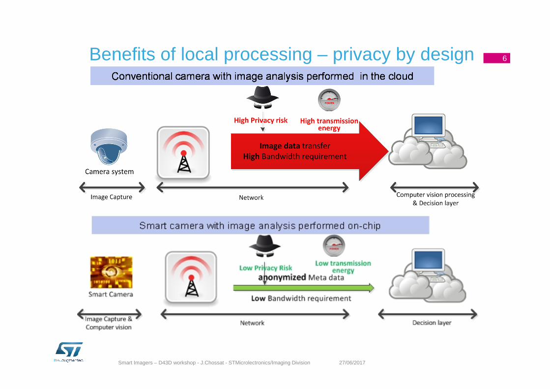
6Benefits of local processing – privacy by design

Smart Imagers – D43D workshop - J.Chossat - STMicrolectronics/Imaging Division 27/06/2017
Rationale for 3D stacking
7
Smart Imagers – D43D workshop - J.Chossat - STMicrolectronics/Imaging Division 27/06/2017
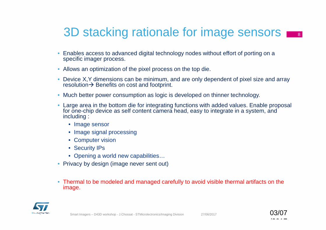
3D stacking rationale for image sensors
• Enables access to advanced digital technology nodes without effort of porting on a specific imager process.
• Allows an optimization of the pixel process on the top die.
• Device X,Y dimensions can be minimum, and are only dependent of pixel size and array resolution� Benefits on cost and footprint.
• Much better power consumption as logic is developed on thinner technology.
• Large area in the bottom die for integrating functions with added values. Enable proposal for one-chip device as self content camera head, easy to integrate in a system, and including :
• Image sensor• Image signal processing • Computer vision• Security IPs• Opening a world new capabilities…
• Privacy by design (image never sent out)
• Thermal to be modeled and managed carefully to avoid visible thermal artifacts on the image.
8
03/07/2017

Smart Imagers – D43D workshop - J.Chossat - STMicrolectronics/Imaging Division 27/06/2017
STMicroelectronics 3D stacked smart imager prototype
9

Smart Imagers – D43D workshop - J.Chossat - STMicrolectronics/Imaging Division 27/06/2017
Image Sensor 3D stack technology
Conventional BSI Imager 3D stacked BSI Imager
• Pixels • Analog & Readout• Sensor Logic
Top die
• Substrate for mechanical support
Bottom die
• Pixels
Top die
• Analog & Readout• Sensor Logic• And more !!!
Bottom die
• Wafer on Wafer stacking
• Hybrid bonding technology
• Passive substrate replaced by advance digital CMOS wafer
• Cut done at Column level – only pixels matrix on the top die.
10

Smart Imagers – D43D workshop - J.Chossat - STMicrolectronics/Imaging Division 27/06/2017
Image Sensor 3D stack technology
3D stacking
• Fine pitch interco thanks to Hybrid Bonding technology• Top die optimized for pixel – keep only pixel layers• Process developed with CEA/Leti
Credits: STM CRL R&D 3D team
TO
P D
ie
Alu pads
Metal3
Metal1
Metal2
Metal4
Metal3
Metal1
Metal2
Meal4
Vx Line
HBVHBP
BO
TT
OM
D
ie
Metal3
Metal1 Metal2
Metal5 Metal4
Metal6
Metal7
Metal3
Metal5
Metal3
Metal1 Metal2
Metal4
Metal6
Metal7
Seal Standard CMOS Pads & Circuits
Stacked Pads
HBPHBV
IO and other circuits
Metal5
Bon
ding
inte
rfac
e11

Smart Imagers – D43D workshop - J.Chossat - STMicrolectronics/Imaging Division 27/06/2017
Hybrid Bonding Interface• 100% yield measured on electrical structures
• Including 30k daisy chains
• Alignment perf <200nm +/-3s
0
0,2
0,4
0,6
0,8
1
-0,5 0 0,5C
um
ula
tive
po
pu
lati
on
(%
)Resistance Delta (%)
1000 Thermal Cycles
(+50°C/+150° C)
BondingInterface
1µm
Credits: STM CRL R&D 3D team

Smart Imagers – D43D workshop - J.Chossat - STMicrolectronics/Imaging Division 27/06/2017
Area budget available on both layers
• Example top and bottom dies breakdown for a • 14Mpix, 1.5um pixel pitch, imager or
• 3.5Mpix 3um device (2x2 pixel grouping) .
Top die
Bottom die
~30mm2 of digital process available for providing
added value !22%
67%
11% Sensor control andADCDigital
Ios
73%
27%
Top Die
Array
Ios and connections
13

Smart Imagers – D43D workshop - J.Chossat - STMicrolectronics/Imaging Division 27/06/2017
3D Stack imager content
Video Timing
ADC
Power management
Y Dec
HDR Processing
ISP
Defect CorrectionColor shading correction
Tone mappingAWB, AE
Color Noise reduction
Mipi CSI
Optical flowaccelerator
Face &Object detection
accelerator
6 cores computer vision processor
CPU
CPU
CPU
CPU
CPU
CPU
Sha
red
mem
ory
11MbitsCentral Memory buffer
MCU
Image processing
Computer vision
Sensor IPs
Peripherals
14
Smart Imagers – D43D workshop - J.Chossat - STMicrolectronics/Imaging Division 27/06/2017
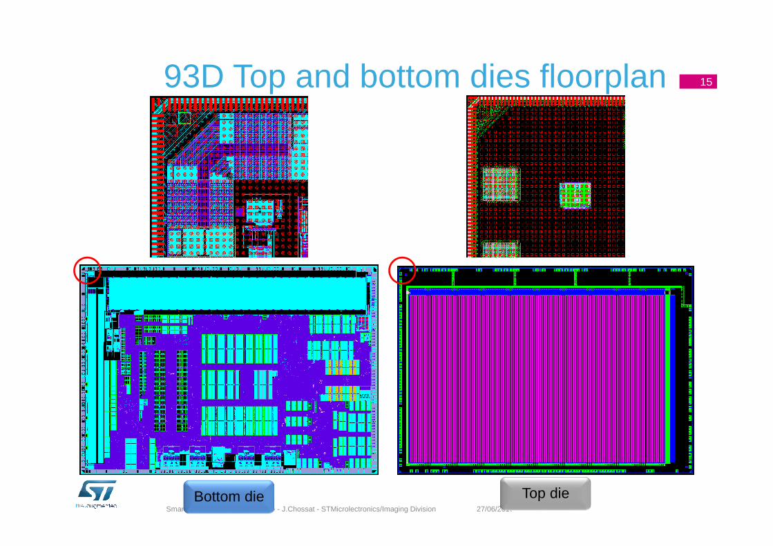
93D Top and bottom dies floorplan
Top dieBottom die
15

Smart Imagers – D43D workshop - J.Chossat - STMicrolectronics/Imaging Division 27/06/2017
93D smart camera use cases shown at CES
Peopleindoor
Optical flow
gender
ageIdentification
Emotions
Faces
16

Smart Imagers – D43D workshop - J.Chossat - STMicrolectronics/Imaging Division 27/06/2017
Power consumption and thermal
Algorithm speed Power
Image Signal Processing
30fps 82mW
Face detection 10fps 39mW
Face Identification 10fps 21mW
Human Body detection 3.6fps 50mW
17
• Goal– To minimize global heating and avoid increasing dark
current– To minimize local heating (hot spots) which could
become visible on the imager.
• Modeling • Measurements
• Architecture– Frequency reduction higher than area increase
� IP dependent gain b/w 10% and 60%
– Easier timing closure at ¼ frequency � saving b/w 10% and 30%
– Can work at lower voltage (e.g. 1.0V instead of 1.1V) � 10% saving
Collaboration with Apache /
Ansysand
CEA-Leti
IP IP
• Area = a• Frequency = F
• Area = ~2.5 * a• Frequency = F/4

Smart Imagers – D43D workshop - J.Chossat - STMicrolectronics/Imaging Division 27/06/2017
Next steps and directions for 3D
18

Smart Imagers – D43D workshop - J.Chossat - STMicrolectronics/Imaging Division 27/06/2017
Convolutional Neural Networks
• State of the Art convolutional neural networks are now delivering high performances for classification and detection.
• Their integration in constrained systems is however still challenging in term of:
• Memory size
• Memory bandwidth/granularity
• 3D is helping as: • Stacking a 3rd layer for increasing total
memory budget
• Providing a direct interconnect b/w a layer of small distributed memories and a layer of HW accelerators.
19
Memory layer
Large banks(regular cores)
Distributed fine grain(CNN and HW acceleration)

Smart Imagers – D43D workshop - J.Chossat - STMicrolectronics/Imaging Division 27/06/2017
3D directions over target markets
• ISO 26262• Image Signal Processing• Minimal thermal dissipation• Security
20
• Pixel quality optimization• X/Y dimensions (Cost and size)• Readout speed• Power consumption
• Ultra low power consumption• Computer vision• Security
• Event based imagers• Global shutter• Flicker free
Smart imagers
Conventional imagers
Specific pixels
Automotive imagers• Mid resolution• Integrated ISP chain• Complex safety features• Advanced low power node• Security functions
• 2 Layers 3D device• Pitch interconnect: med pitch
• Large resolution• Multiple readouts• Some ISP functions• Advanced low power node
• 2 Layers 3D device• Pitch interconnect: med pitch
• Mid resolution• Pixel split on 2 layers
• 2 Layers 3D device used for pixel split
• Pitch interconnect: pix pitch
• Small resolution• Multi-core processing
• Large memories• Neuronal processing
• Many distributed memories
• 3 Layers 3D device• Imager layer• Processing layer• Memory layer
• Pitch interconnect: small pitch
Architectures 3D requirementsMarkets

Smart Imagers – D43D workshop - J.Chossat - STMicrolectronics/Imaging Division 27/06/2017
Thanks for your attention


