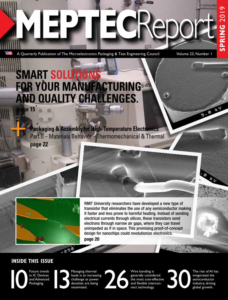
A Quarterly Publication of The Microelectronics Packaging & Test Engineering Council Volume 23, Number 1 -Corp. INSIDE THIS ISSUE 26 Wire bonding is generally considered the most cost-effective and flexible intercon- nect technology. 13 Managing thermal loads is an increasing challenge as power densities are being maximized. 10 Future trends in IC Devices and Advanced Packaging. 30 The rise of AI has invigorated the semiconductor industry, driving global growth. SMART SOLUTIONS FOR YOUR MANUFACTURING AND QUALITY CHALLENGES. page 15 Packaging & Assembly for High-Temperature Electronics Part II – Materials Behavior – Thermomechanical & Thermal page 22 + RMIT University researchers have developed a new type of transistor that eliminates the use of any semiconductor making it faster and less prone to harmful heating. Instead of sending electrical currents through silicon, these transistors send electrons through narrow air gaps, where they can travel unimpeded as if in space. This promising proof-of-concept design for nanochips could revolutionize electronics. page 20 SPRING 2019
Transcript
A Quarterly Publication of The Microelectronics Packaging & Test Engineering Council Volume 23, Number 1
-Corp.INSIDE THIS ISSUE
26Wire bonding is generally considered the most cost-effective and flexible intercon-nect technology.13
Managing thermal loads is an increasing challenge as power densities are being maximized.10
Future trends in IC Devices and Advanced Packaging. 30
The rise of AI has invigorated the semiconductor industry, driving global growth.
SMART SOLUTIONS FOR YOUR MANUFACTURING AND QUALITY CHALLENGES. page 15
Packaging & Assembly for High-Temperature ElectronicsPart II – Materials Behavior – Thermomechanical & Thermalpage 22
+
RMIT University researchers have developed a new type of transistor that eliminates the use of any semiconductor making it faster and less prone to harmful heating. Instead of sending electrical currents through silicon, these transistors send electrons through narrow air gaps, where they can travel unimpeded as if in space. This promising proof-of-concept design for nanochips could revolutionize electronics. page 20
SPRI
NG
201
9
www.amkor.com
Enabling the FutureAs the original pioneers of theOSAT industry, Amkor has helpeddefine and advance the technologymanufacturing and test landscape.We deliver innovative packagingsolutions with the service andcapacity global customers rely on.
MEPTEC Report Vol. 23, No. 1. Published quarterly by MEPCOM LLC, 315 Savannah River Dr., Summerville, SC 29485. Copyright 2019 by MEPCOM LLC. All rights reserved. Materials may not be reproduced in whole or in part without written permission. MEPTEC Report is sent without charge to members of MEPTEC. For non-members, yearly subscriptions are available for $75 in the United States, $80US in Canada and Mexico, and $95US elsewhere. For advertising rates and information contact Gina Edwards at 408-858-5493, Fax Toll Free 1-866-424-0130.
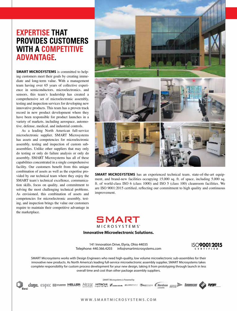
ON THE COVERSMART Solutions for Your Manufacturing and Quality Challenges: As a leading North American full-service microelectronic supplier, SMART Microsys-tems has assets and competencies for microelectronic assembly, testing and inspection of custom sub-assemblies. Unlike other suppliers that may only do testing, only do failure analysis, or only do assembly, SMART Microsystems has all of these capabilities concentrated in a single compre-hensive facility. (see page 15)
10 ANALYSIS – IC packaging technology is being challenged by two distinct, yet closely linked product trends. On one
hand, consumers demand more powerful electronics products – from computers to tablets to smartphones – that provide more features and greater functionality; on the other hand, they want their products to be smaller, lightweight, and ergonomic.
RANDALL SHERMAN, JERRY WATKINS AND FRANK KLOMPNEW VENTURE RESEARCH CORP.
19 TECH BRIEFS – The State-of-the-Art Technology Briefs contains articles from the Binghamton University S3IP
“Flashes.” Binghamton University currently has research thrusts in healthcare/medical electronics; 2.5D/3D packaging; power electronics; cybersecure hw/sw systems; photonics; MEMS; and next generation networks, computers and communications.
DR. GAMAL RAFAI-AHMEDXILINX
15 ENVIRONMENTAL LIFE TEST – The environmental condi-tions in which a product is intended to function need to
be considered carefully. Once these conditions have been deter-mined, a life test profile is defined to simulate the environmental conditions in which the product will need to survive. When the profile is completed, a functional test is performed to evaluate whether the product is still operating to customer specifications.
SMART MICROSYSTEMS
22 PACKAGING – Part I of this series introduced semicon-ductor devices and their general high-temperature capa-
bilities that must be accommodated by assembly and packaging, followed by a glimpse of assembly and packaging materials and technology in regard to high-temperature operation. In Part II thermomechanical and thermal properties will be explored.
DR. RANDALL K. KIRSCHMANR&D CONSULTANT FOR ELECTRONICS TECHNOLOGY
The MEPTEC Report is a Publication of the Microelectronics Packaging & Test
AEHR RECEIVES $2.3M+ IN ORDERS FOR SERVICES AND SUPPORT Aehr Test Systems has announced it has received over $2.3 million in orders for test and burn-in system services and support from a leading multi-national manufacturer of advanced logic integrated circuits (ICs) and analog and mixed signal devices for automo-tive, industrial, communica-tions equipment, enterprise systems and personal elec-tronics applications. “Aehr is committed to support this long-term cus-tomer with the challenges in meeting the ever increas-ing reliability demands of their expanding automotive products line,” said Vernon Rogers, EVP of Sales and Marketing at Aehr Test. Headquartered in Fremont, California, Aehr Test Systems is a world-wide provider of test sys-tems for burning-in and testing logic, optical and memory integrated circuits and has over 2,500 sys-tems installed worldwide.www.aehr.com
ANALOG RANKS #17 AMONG WORLD’S 100 MOST SUSTAINABLE CORPORATIONSAnalog Devices, Inc. has announced that it has been ranked #17 in the Corpo-rate Knights 2019 list of the 100 Most Sustainable Cor-porations in the World. This is the third consecutive year that ADI has risen on the list, having ranked #42 in 2018 and #78 in 2017. “We are delighted to be recognized once again for our strong commitment to economic, environmental, governance, and social sustainability,” said Vincent
Mühlbauer and PragmatIC Announce Strategic Partner-ship Delivering Innovative RFID Manufacturing SolutionsHigh-performance material raises device reliability within challenging environments
MÜHLBAUER, THE proven technology supplier of RFID and smart label pro-duction and personalisation solutions, and PragmatIC, a pioneer in ultra-low cost flex-ible electronics, are pleased to announce their strategic partnership to deliver solu-tions that support the integra-tion of PragmatIC’s unique flexible integrated circuits (FlexICs). The companies have been working together since 2018 building on Mühlbauer’s extensive experience in inlay assembly to develop practi-cal solutions for high speed bonding of FlexICs. The TAL15000 is the industry benchmark system for flip-chip RFID inlay production, with a throughput of up to 13,000 inlays per hour and a
global installed base of more than 300 machines. PragmatIC recently an-nounced its first ConnectIC®
products focused on HF-RFID for smart packaging applications including brand authentication and grey market avoidance. The quali-fication of the TAL15000
for FlexIC assembly enables
manufacturers to leverage their existing installed base to deliver dramatically lower cost RFID inlays. Coupled with the incredibly thin, flexible and robust nature of FlexICs, this unlocks the potential to extend RFID solutions into a much wider range of mass market oppor-tunities. For more information visit www.muehlbauer.de/ ◆
TEXAS INSTRUMENTS HAS INTRODUCED two new Ethernet physical layer (PHY) trans-ceivers, expanding connectivity options for designers of both space-constrained applica-tions and time-sensitive networks (TSNs). The DP83825I low-power 10-/100-Mbps Ethernet PHY has a 44 percent smaller pack-age size than competing devices and provides a 150-meter cable reach. The DP83869HM is the industry’s only gigabit Ethernet PHY that supports copper and fiber media, and offers high-temperature operation up to 125°C, which enables engineers to leverage the speed and reliability of gigabit Ethernet connectivity in harsh environments. These devices join TI’s extensive portfolio of Ethernet PHY transceivers and empower designers to implement connectivity in a vari-ety of challenging designs. The small pack-age, low power consumption and long cable reach of the DP83825I enable designers to reduce the size and cost of compact IP network camera, lighting, electronic point-of-sale and other space-constrained applications without sacrificing network reach. The high operating
temperature of the DP83869HM, as well as its electrostatic discharge (ESD) immunity and support for media conversion, help increase performance and design flexibility in factory automation, motor drive and grid infrastructure equipment designs. Texas Instruments Incorporated (TI) is a global semiconductor design and manufactur-ing company that develops analog integrated circuits (ICs) and embedded processors. Learn more at www.ti.com. ◆
TI’s new Ethernet PHYs Simplify Design and Optimize Network Performance
Roche, President and CEO, Analog Devices. “At ADI, we have long prided our-selves in setting increas-ingly ambitious goals in these areas and driving aggressively to meet and exceed them across our global footprint.”www.analog.com
ASE’S CHAIRMAN RECEIVES HONORARY DOCTORATE DEGREE ASE is pleased to an-nounce that Chairman Jason Chang was pre-sented the Honorary Doctorate Degree by the prestigious National Sun Yat-sen University in honor of his entrepreneurship and extensive contribution to the semiconductor industry. Jason founded ASE in 1984 together with his brother, Richard. They established the first facil-ity in Kaohsiung, Taiwan with only 200 persons. The Kaohsiung campus has since grown to a head-count of 26,000 employees, while globally ASE has over 93,000 employees. Jason believes firmly in human capital and is committed to cultivating talent across the organization. In recognition of his focus and commit-ment, Jason was presented the Dale Carnegie Leader-ship Award in 2017. In 2015, Jason received the SEMI award for his suc-cessful commercialization of copper wire that has enabled the development of affordable and high per-formance consumer end-products. As the Chairman and CEO of the world’s leading semiconductor manufactur-ing service provider, Jason has inculcated in his team the value of sustainability and corporate citizenship. www.aseglobal.com
XILINX, INC. AND SAMSUNG ELECTRONICS Co., Ltd., have announced an expanded collabo-ration that has resulted in the world’s first 5G New Radio (NR) commercial deployment. This world-first deployment is in South Korea and will be followed by additional countries globally in 2019 and beyond. Xilinx and Samsung have been working together to develop and deploy multiple 5G Massive Multiple-input, Multiple-output (mMIMO) and millimeter wave (mmWave) solutions using the Xilinx® UltraScale+™ plat-form. Additionally, Samsung is collaborating with Xilinx on its forthcoming Versal® adapt-able compute acceleration platform (ACAP) products to deliver state-of-the-art 5G solutions. The goal is to address a multi-fold increase in compute density requirements in next-generation 5G mMIMO systems while enabling the use of machine learning algorithms to maximize the benefits of beamforming gains to further boost capacity and performance.
“Our strong relationship with Samsung spans many years and we’re very proud to be a part of the 5G NR commercial deployment in addition to expanding our relationship with the company on our Versal platform,” said Liam Madden, executive vice president of hardware and sys-tems product development, Xilinx. “We are com-mitted to providing our customers with solutions that drive high value services and look forward to our continued collaboration with Samsung.” “Through a joint initiative from close collabo-ration with a trusted partner, Xilinx, Samsung was able to successfully supply the state-of-the-art products that were essential in 5G com-mercialization,” said Jaeho Jeon, executive vice president and head of R&D, networks business, Samsung Electronics. “Taking full advantage of our resources and gearing up with our 5G solu-tions, Samsung will take a leap forward in pro-viding immersive user experiences and enriching the life of next-generation technologies.” Visit www.xilinx.com for more information. ◆
SKYWORKS SOLUTIONS, Inc., an innovator of high per-formance analog semiconduc-tors connecting people, places and things, today introduced Sky5™ LiTE – the industry’s first fully integrated front-end solution for mass tier 5G cellular applications. With improved RF performance in a uniquely compact pack-age, Skyworks’ newest device simplifies designs, enabling faster deployment. The base-band agnostic platform sup-ports up to 100 MHz wide bandwidth of 5G new radio (NR) waveforms with flexible power management options – delivering high-speed network experiences with optimized efficiency and near zero latency. Targeted for mass markets, Sky5™ LiTE interfaces with all leading chipset providers and equips early 5G adopters with differ-entiated architectures for an open ecosystem – the favored
approach when compared with closed, sole-sourced RF front-end products. With the recent introduction of Sky5™ Ultra for premium applica-tions, Skyworks offers the most comprehensive 5G port-folio in the market. All Sky5™ solutions support new 5G NR wave-forms and spectrum in addition to enhanced carrier aggregation and 4G/5G dual connectivity, while deliver-ing exceptional levels of inte-
Xilinx and Samsung Jointly Enable the World’s First 5G NR Commercial Deployment
gration and performance. Skyworks is a global company with engineering, marketing, operations, sales and support facilities located throughout Asia, Europe and North America and is a member of the S&P 500® and Nasdaq-100® market indices. For more information about Sky5™ LiTE and our comprehensive Sky5™ port-folio, visit www.skyworksinc.com or contact [email protected]. ◆
Skyworks Launches Sky5™ LiTE for Universal 5G DeploymentsFirst high-performance platforms to support mass market devices
INFINEON APPOINTS DR. SVEN SCHNEIDER TO CFO MAY 2019The Supervisory Board of Infineon Technologies AG has appointed Dr. Sven Schneider to become the CFO effective 1 May 2019. His contract will initially run for three years. Dr. Schnei-der is moving to Infineon from Linde AG, where he is currently Board Spokes-man, CFO and Labor Director. Schneider succeeds Dominik Asam, who will be moving to Airbus SE on 1 April. During the transition period, the CEO of Infineon Technologies AG, Dr. Rein-hard Ploss, will manage the company’s finance organi-zation. As Chief Financial Officer, Dr. Schneider will be in charge of Accounting & Reporting, Financial Con-trolling, Financial Planning, Investor Relations, Taxes, Treasury, Auditing, Compli-ance, Export Control, Risk Management, Business Continuity, and Information Technology.www.Infineon.com
DISCO RECEIVES PRESTIGIOUS INTEL QUALITY AWARDDISCO Corporation has been recognized by Intel Corporation as a recipi-ent of its prestigious 2018 Supplier Continuous Qual-ity Improvement (SCQI) award. The SCQI award is Intel’s most prestigious recognition and signifies an elite performance in all critical management sys-tems supporting quality, cost, availability, technol-ogy, customer service, and sustainability. Companies like DISCO that receive this award are considered to be industry role-models that provide unparalleled supply
The announcement sees the strengthening of ON Semiconductor’s comprehen-sive and growing SiC ecosys-tem that features complemen-tary devices including SiC diodes, and SiC drivers, plus vital resources such as device simulation tools, SPICE models and application infor-mation to help design and systems engineers meet their high frequency circuit devel-opment challenges. ON Semiconductor’s 1200 volt (V), 80 milliohm (mΩ), SiC MOSFETs are rugged and align with the needs of modern high fre-quency designs. They com-bine high power density with highly efficient operation that can significantly reduce operating costs and overall system size due to smaller device footprints. These characteristics also mean less thermal management is required, further reduc-ing bill of materials (BoM)
ON SEMICONDUCTOR, driving energy efficient innovations, has introduced two new silicon carbide (SiC) MOSFET devices. The industrial grade NTHL080N-120SC1 and AEC-Q101 auto-motive grade NVHL080N-120SC1 bring the enabling, wide-ranging performance benefits of wide band gap technology to important high growth end application areas such as Automotive DCDC and onboard charger applica-tions for electric vehicles as well as solar, and uninter-ruptible and server power supplies.
costs, size and weight. Key features and associ-ated design benefits of the new devices include class-leading low leakage cur-rent, a fast intrinsic diode with low reverse recovery charge, which gives steep power loss reduction and supports higher frequency operation and greater power density, and low Eon and Eoff / fast turn ON and OFF combined with low forward voltage to reduce total power losses and therefore cooling requirements. Low device capacitance supports the ability to switch at very high frequencies which reduces troublesome EMI issues; meanwhile, higher surge, avalanche capability, and robustness against short-circuits enhances overall ruggedness, gives improved reliability and longer overall life expectancy. For more information, visit www.onsemi.com. ◆
ON Semiconductor Introduces New Industrial and Automotive Qualified SiC MOSFETsComplementing a Growing Ecosystem and Bringing Wide Band Gap Performance Benefits to Rapid Growth Applications
SMI (SILICON MICROSTRUCTURES, INC.) is pleased to announce that biocompatibility of IntraSenseTM has been confirmed at a major medical device manufacturer. Biocompatibil-ity is a critical factor during the design of an invasive medical device and the compliance of IntraSenseTM parts ensures easy integration into a variety of minimally invasive applica-tions. The IntraSenseTM line of pressure sensing solutions simplifies direct pressure monitoring throughout the anatomy leveraging indus-try leading size of less than 1-French. It is designed to enable accurate in vivo pressure sensing in many minimally invasive devices, including catheters and endoscopes. To ensure easy system integration, the sensor can be directly exposed to different bodily fluids with no encapsulation required. IntraSenseTM bio-compatibility and stable performance has now been confirmed through extensive testing.
“Independent testing by third parties is an important part of our product development,” explains Dr. Justin Gaynor, Vice President, IntraSenseTM Product Line. “Our customer con-firmed that their device, in which IntraSense is exposed directly to the bloodstream, showed reactivity grades of zero for cytotoxicity, sensitization and intracutaneous reactivity. It was rated non-toxic, non-pyrogenic and non-hemolytic. Finally, it was found non-activating in thrombolytic and SC5b-9 tests. For visit www.si-micro.com. ◆
chain support to Intel. “I am honored to recog-nize the winners of Intel’s Supplier Continuous Qual-ity Improvement award for 2018,” said Randhir Thakur, corporate vice president and general manager of Global Supply Chain at Intel. “These suppliers continuously display their commitment to Intel and collaborate deeply with us to delight our customers. The SCQI award dis-tinguishes best-in-class standards of service, responsibility, and integrity. To qualify for SCQI status, Intel suppliers must exceed the highest expectations and aggressive perfor-mance goals while scoring at least 95 percent on an integrated report card that assesses performance throughout the year. www.discousa.com ◆
ceiver bandwidth perfor-mance when compared to traditional solutions. It is critical for applications where high bandwidth is paramount, including: net-working, cloud and 5G appli-cations, optical transport net-works, enterprise network-ing, cloud service providers, and 5G. By supporting dual-mode modulation, 58Gbps PAM4 and 30Gbps NRZ, new infrastructure can reach 58Gbps data rates while staying backward-compatible with existing network infra-structure.
THE INTEL STRATIX 10 TX FPGAs are the world’s first field programmable gate array with 58Gbps PAM4 transceiver technology enab-ling 400Gb Ethernet deploy-ment. This technology dou-bles transceiver bandwidth performance when compared to traditional solutions. At the Optical Fiber Communications (OFC) con-ference in San Diego March 11-15, Intel’s Programmable Solutions Group showcased market-leading 58Gbps transceiver technology inte-grated on the Intel® Stratix® 10 TX FPGA – the world’s first field programmable gate array (FPGA) with 58Gbps PAM4 transceiver technol-ogy now shipping in volume production and enabling 400Gb Ethernet deployment. This industry-leading technology doubles trans-
To facilitate the future of networking, Network Func-tion Virtualization (NFV) and optical transport solu-tions, Intel Stratix 10 TX FPGAs provide up to 144 transceiver lanes with serial data rates of 1 to 58Gbps. This combination delivers a higher aggregate bandwidth than any current FPGA, enabling architects to scale to 100Gb, 200Gb and 400Gb delivery speeds. Intel Stratix 10 FPGA 58Gbs transceivers are interoperable with 400G Ethernet FPGAs, using only eight channels to support new high-bandwidth require-ments for routers, switches, active optical cables and direct attach cables, intercon-nects, and test and measure-ment equipment. For more information go to www.intel.com . ◆
Intel Stratix 10 TX
Promex develops unique heterogeneous assembly processes for manufacturing Medical,
Biotech & Complex DevicesStart with a FREE Promex design review for reliability & manufacturability
• Class 100 & Class 1000 cleanroom assembly environments (ISO 5 & ISO 6)
• Solidworks for design review, simulating process capability & tooling fabrication
• Flip chip (Cu pillar/solder balls) assembly• Fine-pitch thermocompression assembly• Al & Au wirebonding (low temp) • Ultra-thin die (backgrinding, dicing & die attach)• Mechanical part assembly on wafer• Fluid channel sealing • Assembly at low temperature (< 85°C)• ITAR, ISO 13485:2016, ISO 9001: 2015 & IPC 610
certified, Calif. FDB Medical Device Manufacturing License
Electronic coupling is the transfer of ener-gy from one circuit or medium to another. Sometimes it is intentional and sometimes not (crosstalk). I hope that this column, by mixing technology and general observa-tions, is thought-provoking and “couples” with your thinking. Most of the time I will stick to technology but occasional cross-talk diversions may deliver a message closer to home.
Look Beyond the Small Screen to Get the Big Picture!
COUPLING & CROSSTALKBy Ira Feldman
THE ELECTRONICS INDUSTRY IS in a transition forced by rapid changes in computer hardware and concepts. How-ever, there is even more change on the horizon and this historical perspective can help you to understand and plan for the future. The earliest ‘big iron’ computer sys-tems were built to solve specific scientif-ic and computational problems. UNIVAC in the 1950s, marked the beginning of general purpose ‘commercial’ computing systems. The software applications were limited by the capability of the general-purpose mainframes and minicomputer hardware. As hardware became faster, enabling more powerful software, rapid adoption occurred in many industries. But for non-scientific use, hardware fully defined and limited the practica-bility of software and applications. In the 1980s and 90s, computing shifted from mainframes to personal computers (PCs). The economies of scale made it feasible for individuals to have their own computers. And widespread corporate deployments to the desk of each employee quickly followed since the productivity gain far exceeded the cost. Computing moved out of the data center and was fully decentralized with this new model of personal computing. Users started to demand and define their own needs! As a result, software engineers responded to these needs with-in the limitations of the hardware. Then, as today, PC manufacturers
relied on Intel to supply the research and development (R&D) to drive improve-ments in the system architecture. These suppliers have simply become ‘box assemblers’ competing in the market with the lowest cost brand name or white box system. In the end, Intel sets the product specifications and features of their micro-processors which in turn defines the system’s performance. However, appli-cations are still limited by the available computational hardware and architecture. With annual volumes approximately five times that of PCs, smartphones are currently the engine powering semi-conductor industry growth. Within the robust competition in the smartphone marketplace there is a never-ending quest for improved functionality (including increased processing power, better qual-ity displays, and longer battery life) and product differentiation to keep or gain market share. Even with such hardware improvements the main operating sys-tems, Android and iOS, are still limited by the hardware functionality. Today smartphones are where the consumer sees innovation taking place. Users are enthralled as new features such as 3D face identification and folding displays are added. Looking ahead the baseband processor and associated radio frequency (RF) ‘front end’ will need to change significantly to support 5G. Not to mention if / when millimeter wave (mmWave) mesh networking is imple-mented as part of 5G. And there contin-ues to be advanced packaging innovation including 2.5D and 3D integration, wafer level chip scale packaging (WLCSP), and panel level processing (PLP) to improve performance and lower costs. From a system architecture perspec-tive however, smartphones and PCs due to their general-purpose nature have become static. The core system design of a smartphone is not much different than a forty-year-old PC design centered around a processor with a traditional von Neu-mann architecture. So, where is the real innovation in system architecture and semiconductors occurring? It’s in the cloud! And the cloud has flipped the paradigm in terms of the application defining the hardware instead of being limited by it. Regardless of what you call them, the ‘Super 7’ (Intel’s term) or the Hyper-scale 8 operate data centers on a scale orders of magnitude larger than other companies. Alibaba, Amazon, Apple,
Baidu, Facebook, Google, Microsoft, and Tencent all have hyperscale data centers. Operating on the scale of millions of servers has required significant engineer-ing at all levels to cost-effectively build and run these data centers. These hyperscale companies have also pared back their computing equip-ment to only the essentials, eschewing any non-essential feature and eliminat-ing all cosmetic items. Never going to attach a display to a server? Eliminate the display driver circuitry. Plastic bezels or fancy sheet metal? Gone. In this vein, the hyperscale companies have developed their own supply chain using electronic manufacturing service (EMS) providers to build their own systems and bypass traditional server companies like Hewlett-Packard and Dell. The scale of their purchasing makes it economical to obtain servers and other equipment with just the minimum required features at the lowest possible cost. Facebook and Microsoft have gone one step further by setting up the Open Compute Project to ‘open source’ their hardware designs to further increase innovation and econo-mies of scale. Beyond operational and supply chain ‘improvements’, significant investments have also been made by the hyperscale operators in new types of computational architecture and hardware. They have developed “private hardware” to enable specific end applications. For example, the deployment of machine learning has required substantial addi-tional computing power. Graphical pro-cessor units (GPUs) have been success-fully tasked with some of this computing load. So well in fact that Nvidia has repositioned its GPU products and com-pany from being a graphics card provider to a machine learning company that also makes graphics cards. Microsoft, Facebook, and others have turned to field programmable gate array (FPGA) co-processors to further acceler-ate machine learning computing. And Google calculated in 2013 that it would need to double their data centers to han-dle their machine learning load if they didn’t change their computing equip-ment. So Google developed their own application specific integrated circuit (ASIC) with a unique architecture suited for neural networks. Their initial Tensor Processor Unit (TPU) provided an “order of magnitude” greater computing power for machine learning applications per
watt of power than a traditional server. And Google has provided customer access to their third generation TPUs via their cloud services. Facebook’s Chief Artificial Intel-ligence (AI) Scientist, Yann LeCun, at the recent IEEE International Solid State Circuits Conference (February 2019), described how they need new machine learning (deep learning) hardware to continue to make advances. He stated that different processor architectures are needed along with changes in the way arithmetic is done in circuits to increase efficiency. Not only is Facebook discuss-ing basic circuity, they have created their own in-house chip design team to do the research and development to build the hardware they desire or require. Why does it make sense for a ‘social media’ giant and the other hyperscale cloud operators to go all the way down to the gate level on their hardware? Their computational needs are very specific and they must obtain greater efficiency than can be provided by general purpose computing hardware. Since they operate on such a large scale – both in terms of computing units purchased and power
consumed – they can justify the tens to hundreds of million dollar investments to build private hardware including custom leading-edge ASICs. In an effort to gain an advantage over their competitors, the hyperscale companies will continue to push non-traditional architectures and other proprietary innovations. The new frontier of computing inno-vation now resides in the hyperscale data centers. The pendulum has swung back to the ‘big iron’ from the distributed computing environment with a twist. “Software” and “social media” compa-nies now need solution architects and hardware experts to develop the most efficient computing platforms to serve the needs of their applications. And hard-ware companies need consultants and connections to the hyperscale companies to understand the needs of the applica-tions to properly position their technol-ogy for consideration. Unlike consumer and commercial products, we will only see the details of these proprietary solu-tions when the cloud providers wish to let the sun shine through. While most people were busy star-ing down at their smartphone screens,
they didn’t glance up to see the con-centration of computing power move to ‘the cloud’. Now you need more - the ability to see the direction the wind is blowing these clouds and what can be done to “make it rain” on your company! For more of my thoughts, please see my blog http://hightechbizdev.com. As always, I look forward to hearing your comments directly. Please contact me to discuss your thoughts or if I can be of any assistance. ◆
IRA FELDMAN is the Principal Consultant of Feldman Engineering Corp. which guides high technology products and services from concept to high volume manufacturing. He engages on a wide range of projects including technical marketing, prod-uct-generation processes, supply-chain management, and business development. ([email protected])
Conference Sponsors:
For more information, visit:
www.ectc.net
Don’t Miss Out on the Industry’s Premier Event!
The only event that encompasses the
diverse world of integrated systems packaging.
MORE THAN 350 TECHNICAL PAPERS
COVERING:Fan-Out WLP & CSP 3D & TSV Processing
Heterogeneous Integration Fine Pitch Flip-ChipMEMS & Sensors
Advanced Substrates Advanced Wire Bonding
Flexible & Wearable Devices RF Components
Automotive ElectronicsHarsh Environment
Bio/Medical DevicesThermal/Mech Simulation
Interconnect ReliabilityOptical Interconnects
HIGHLIGHTSn41 technical sessions
including:
•5 interactive presentation sessions, including one featuring student presenters
n18 CEU-approved Professional Development Courses
nTechnology Corner Exhibits, featuring more than 100 industry-leading vendors
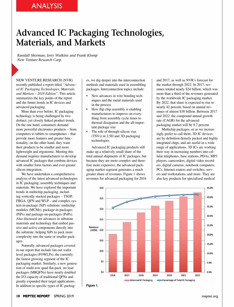
NEW VENTURE RESEARCH (NVR) recently published a report titled “Advanc-ed IC Packaging Technologies, Materials and Markets – 2018 Edition”. This article summarizes the key points of the report and the future trends in IC devices and advanced packaging. More than ever before, IC packaging technology is being challenged by two distinct, yet closely linked product trends. On the one hand, consumers demand more powerful electronics products – from computers to tablets to smartphones – that provide more features and greater func-tionality; on the other hand, they want their products to be smaller and more lightweight and ergonomic. Meeting this demand requires manufacturers to develop advanced IC packages that combine devices with smaller form factors and ever-greater silicon integration. We have undertaken a comprehensive analysis of the latest advanced technologies in IC packaging, assembly techniques and materials. We have explored the important trends in multichip packaging, includ-ing vertically stacked packages – TSOP, FBGA, QFN and WLP – and complex sys-tem-in-package (SiP) solutions: multichip modules (MCMs), package-in-packages (PiPs) and package-on-packages (PoPs). Also discussed are advances in substrate materials and technology that embed pas-sive and active components directly into the substrate, helping SiPs to pack more complexity into the same or smaller pack-ages. Naturally, advanced packages covered in our report that include fan-out wafer level packages (FOWLPs), the currently the fastest growing segment of the IC packaging market. Similarly, a new genera-tion of multi-row quad flat-pack, no lead packages (MRQFNs) have nearly doubled the I/O capacity of traditional QFNs and greatly expanded their target applications. In addition to specific types of IC packag-
Advanced IC Packaging Technologies, Materials, and Markets Randall Sherman, Jerry Watkins and Frank Klomp New Venture Research Corp.
es, we dig deeper into the interconnection methods and materials used in assembling packages. Interconnection topics include:
• New advances in wire bonding tech- niques and the metal materials used in the process• How flip chip assembly is enabling manufacturers to improve on every- thing from assembly cycle times to thermal dissipation and the all-impor- tant package size• The role of through-silicon vias (TSVs) in 2.5D and 3D packaging technologies
Advanced IC packaging products still make up a relatively small share of the total annual shipments of IC packages, but because they are more complex and there-fore more expensive, the advanced pack-aging market segment generates a much greater share of revenues. Figure 1 shows revenues for advanced packaging for 2016
and 2017, as well as NVR’s forecast for the market through 2022. In 2017, rev-enues totaled nearly $24 billion, which was more than a third of the revenues generated by the worldwide IC packaging market. By 2022, that share is expected to rise to nearly 42 percent, based on annual rev-enues of almost $38 billion. Between 2017 and 2022, the compound annual growth rate (CAGR) for the advanced packaging market will be 9.7 percent. Multichip packages, or as we increas-ingly prefer to call them, 3D IC devices, are by definition densely packed and highly integrated chips, and are useful in a wide range of applications. 3D ICs are working their way in increasing numbers into cel-lular telephones, base stations, PDAs, MP3 players, camcorders, digital video record-ers, digital cameras, notebook computers, PCs, Internet routers and switches, serv-ers and workstations, and more. They are also key products for specialized medical
applications, where companies are looking for highly miniaturized packages that can be used for insertion into the body, such as cochlear hearing aids. 3D ICs will be the building blocks of a variety of communication devices, data centers, routers and sensors that access and support the Internet of Things (IoT) over 5G broadband networks. The IoT, often augmented and enhanced by Arti-ficial Intelligence (AI) capabilities, will contribute to the growth of new consumer and industrial applications, such as edge computing, autonomous cars, healthcare monitoring devices, interactive gaming, smart home appliances, etc. Semiconductor technology requires electronics manufac-turers to adapt to a new reality, realign their strategic and operating plans in order to bring to market billions of connected devices and interdependent systems.1 A complete transition to vertical device structures, combining memory and logic, is expected to evolve over the years to come. This affects the entire electronics supply chain, ranging from OEMs and IDMs to Foundries, OSATs, EMS providers, PCB vendors and assembly equipment suppli-ers. System integrators will set the design requirements and device specifications at the beginning of each product cycle, stipu-lating volume, cost, delivery time, yield to defect ratios, etc. Manufacturing partners must be ready to execute, using innova-tive automation strategies that increase production flexibility, improve operational efficiency and product quality to meet the changing needs of customers and maintain their competitiveness in the industry. Drawing on the insights of STATS ChipPAC 2, 3D IC integration, driven by mobile applications and high-performance computing and networking, is progressing on three fronts at the same time, starting with the package level, the wafer-level and more recently at the silicon level. By combining Embedded Wafer Level BGA (eWLB) and Fan-Out Wafer Level Packag-ing (FO-WLP) technology with Through Silicon Via (TSV) and Integrated Passive Device (IPD) technology, the industry is achieving heterogeneous integration in a wide range of design configurations. Given
constraints in the Front-end of line (FEOL) and the Back-end of line (BEOL), the Mid-end of line (MEOL) process flow may be best suitable to the assembly requirements, especially with the integration of memory and logic devices at advanced technology nodes. (see Figure 2) In advanced 3D stacking technologies, an important step is to develop fine pitch and high-density solder micro bumps for Flip Chip (FC) interconnect. Die attach-ment to the PCB is usually carried out with thermo-compression FC bonders in a controlled collapse chip connection (C4). Passive devices such as resistors, capaci-tors, filters and resonators are key building blocks of RF circuitry, but are also relative-ly large devices, consuming 70% or more of the available board space in some cases. This is a powerful argument for combining IPD with TSV, integrating (stacking) pas-sive components to save space and limit the overall package footprint. In the FO-WLP workflow, chips are processed on a wafer in the Foundry and diced at the OSAT. Using High Density SMT machines, the dies are picked from the wafer onto a metal carrier, which is encapsulated by an epoxy molded com-pound to produce a reconstituted wafer, usually in a 300mm round format. The fan-out manufacturing process, such as the formation of RDL layers and bumping to form external I/O terminals, is conducted on the reconstituted wafer. Then, the molded package is separated and the dies are cut, forming a finalized chip in a fan-
out package. Beyond smartphones (Apple, Xiaomi), the technology is being used in the automotive market to enable Advanced Driver Assistance Systems (ADAS), using NXP, Freescale and Infineon 10mm pack-ages. Die assembly processing costs, ex-cluding the cost of the die itself, may reach some 15% of total packaging costs because both FC bonding and mixed IC / SMT assembly are quite expensive. Since the material contribution of the populated substrate comprises approximately 30 to 60% of the entire packaging cost, IDMs and OSATs are working with substrate suppliers and considering Fan-Out Panel Level Packaging (FO-PLP) to employ more die in larger area formats. While still immature, Samsung Electro-Mechanics, ASE, PTI and JCET / STATS ChipPac are experimenting with FO-PLP technology, which, should their focus shift from PCB to TF substrates and assembly, could result in cutting some of the less scalable process steps in 3D IC integration. In the production of handheld devices such as mobile phones and tablets, the traditional boundaries between transistor manufacturing, interconnect, packaging and assembly are blurring. Driven by 3D IC integration, we are witnessing a conver-gence of Wafer processing, IC packaging and PCB assembly operations. This is because, in the interconnection of vertical structures, such as TSVs and bumps, the equipment and process steps during differ-ent stages of production must be compat-ible. For the OSATs to remain competitive in the WLP era, they must now provide customers with a much higher level of
continued on page 25
1 According to different sources, the IoT market could generate $3.9 trillion (low estimate) to $11.5 trillion (high estimate) in the next decade. The semiconductor industry could realize $50 billion to $75 billion in value from IoT-related products, ranging from chip sets to mini-systems.2 Thin SiP and 3D eWLB (embedded Wafer Level BGA) - STATS ChipPAC, ICEP-IAAC Proceedings
Figure 2. (Source: United Microelectronics Corporation)
the die attach paste materials used must be compatible with long post-dispense times while awaiting die placement and adhesive curing. This time after material deposition and prior to die placement is referred to as ‘open time’ and, if the paste does not have a long open time and dries out or cures from exposure, poor wetting, incomplete fillets or inconsistent bond line thicknesses may result and adversely affect reliability. LOCTITE ABLESTIK ABP 8068T’s stage time – the time after the die is bonded but before the material is cured – is also very forgiving in order to achieve optimal manufacturability. The adhesion performance of the
sintering and resin matrix curing. The new, patent-pending LOCTITE® ABLESTIK®
ABP 8068T semi-sintering die attach paste series has successfully addressed the regulatory challenges of high-lead solders, thermal conductivity drawbacks of conven-tional die attach pastes, and processability shortcomings of sintering products that require high pressure.
Processability and Performance Ease-of-use is a key advantage of LOC-TITE ABLESTIK ABP 8068T materials; they can be processed with existing meth-ods, allowing use of needle dispensing and/or printing platforms and standard bonding equipment for maximized UPH. There is no requirement to invest in additional equipment or change current processes; the pressure and high heat needed to achieve sintering with some sintering products aren’t necessary. Henkel’s semi-sintering materials exhibit no missing dots, paste separation or adhesion degradation after 24 hours of continuous dispensing. Excellent resin bleed out control on different lead frame surfaces is also a characteristic of the new semi-sintering die attach pastes. In many cases, high power applications integrate miniaturized packages where multiple packages are processed on a sin-gle strip. Because of this serial approach,
NO MATTER WHERE YOU LOOK, IT seems that nearly every part of the elec-tronics sector is being impacted by the integration of smaller, higher-functioning devices. Smartphones, data centers, auto-mobiles, airplanes, smart home systems and even gaming devices are all packing massive capability into more compact spaces. As consumers, we love what this brings to our lives. As designers and manu-facturers, we understand what this brings to the device – more heat! Thermal man-agement isn’t a new concern; effectively dissipating heat has always been a key component of reliable operation. Today, however, power densities are being maxi-mized, making managing the thermal load increasingly challenging. While thermal interface materials are a large part of the equation at the board level, die level thermal management is also an important element of optimized device reliability. Until recently, high thermal die attach solutions were limited to high-lead solders which are subject to impending environmental phase-out legislation; or, silver sintering materials that require inte-gration of complex processes. Even previ-ous generation, so-called high thermal die attach pastes have been unable to deliver ultra-high thermal conductivity because of silver filler interface contact limitations. With these shortcomings understood, Henkel materials scientists embarked on a development project to formulate a high thermal die attach portfolio that is pro-cessed as easily as standard die attach and provides the high thermal conductivity of high-lead solder and pure silver sintering, while delivering the reliability character-istics of resin-based die attach pastes. The result is a semi-sintering – also referred to as hybrid sintering – die attach paste that allows simultaneous silver particle
High Thermal Semi-Sintering Die Attach PasteNo Solder, No Pressure, No Problem Raj Peddi, Henkel Corporation
Consistent Printing and Dispensing for 24 Continuous HoursGood printability and consistent dispensingwith no separation or missing dots
indicating it is a viable replacement for solder materials. Finally, because of LOCTITE ABLES-TIK ABP 8068T’s ability to bind the silver sintered structure in its unique resin matrix, the semi-sintering materials do not exhibit the brittleness of pure silver sintered mate-rials. This makes Henkel’s semi-sintering portfolio applicable to a wide die size range, providing high elongation (tough-ness) for better thermal cycling perfor-
LOCTITE ABLESTIK ABP 8068T series semi-sintering pastes on various die sizes (as large as 5 mm x 5 mm) and lead frame finishes (including Ag, Cu, PPF and Au) is also robust. In addition, thermal conductiv-ity of the material when cured at 200°C is 110 W/m-K, which is comparable to pure silver sintered materials.
Reliability As in-package thermal conductivity is a more accurate predictor of reliability performance than standard bulk thermal conductivity measurements, an in-package thermal test was conducted to evalu-ate LOCTITE ABLESTIK ABP 8068T within a functional QFN package. The semi-sintering material exhibited better in-package thermal performance than tra-ditional Ag-filled die attach adhesives on all lead frame surfaces – even Cu, where conventional materials struggle to form an intermetallic layer and have high interfacial thermal resistance. Here, the semi-sintering die attach paste showed in-package thermal resistance similar to that of soft solder,
mance and, therefore, reliability. For more information about Henkel’s novel semi-sintering die attach pastes, download our recent webinar (https://www.henkel-adhesives.com/us/en/insights/all-insights/events-webinars/high-thermal-die-attach-webinar.html) and/or visit Henkel’s semi-sintering product page (https://www.henkel-adhesives.com/us/en/products/industrial-adhesives/die-attach-adhesives/semi-sintering-die-attach-paste.html). ◆
W W W . S M A R T M I C R O S Y S T E M S . C O M
CUSTOM ENVIRONMENTAL LIFE TEST & FAILURE ANALYSIS
SMART SOLUTIONS FOR YOUR MANUFACTURING AND QUALITY CHALLENGES.Improve Yield and Reduce Overall Manufacturing Costs Using SMART Microsystems In-House Expertise and Resources for Custom Microelectronic Assembly, Testing and Inspection.
ROOT CAUSE ANALYSIS AND TEST FOR MICROELECTRONIC ASSEMBLIES TO REDUCE COST.
In the world of new product development, failure analysis is valuable tool that can reduce costs and accelerate time to market. Failure analysis can be used to achieve a better understanding of the be-havior of a microelectronic assembly after being stressed by the conditions from its application environment. In a thoughtful design, the environ-mental conditions in which a product is intended to function need to be considered carefully. Once these conditions have been determined, a life test profile is defined in order to simulate the environ-mental conditions in which the product will need to survive. When the life test profile is completed, a functional test is performed to evaluate whether the product is still operating according to customer specifications. The next step is to perform destruc-tive and/or non-destructive analysis of the product to identify its strengths and weaknesses. Analysis should always be conducted regardless of whether or not there is a confirmed failure. In this stage of the new product development cycle a complete “lessons learned” review is in order. It is important to use all collected data to drive design and process improvements. This aligns with proven new product development strategies such as: test early, test often and concurrent engineering. The idea is to create early learning using failure analysis results in order to implement improvements before freezing the product design. The results of this “lessons learned” review drive action in the form of a Risk Analysis, PFMEA, DFMEA, other six sigma techniques and quality methods. Failure analysis is an effective tool for the development of microelectronic assemblies for new products.
2
COMPLETE CMM PRECISION DIMENSIONAL INSPECTION TO MANAGE INCOMING MATERIAL QUALITY.
A s new products and components continue to miniaturize in the growing and expand-ing microelectronics field, the test and measurement requirements have become
more demanding. Finding solutions to these stringent measurement requirements is crucial to maintaining quality products, and to accelerate the design and development processes. Full service suppliers must not only provide microelectronic assembly ser-vices, but also perform life and environmental testing, as well as precision measure-ment, functional testing, and final inspection. Exposure to this full service type of prod-uct development creates a unique perspective on the demands and benefits of including precision measurement which can bring added value to a customer. When considering a suite of potential measurement systems provided by a full service supplier – such as optical inspection, CSAM, 3D X-ray, interferometry, and SEM – it is important to be able to measure the smallest detail features with precision and accuracy. For mechani-cal assemblies used for microelectronic packaging, a coordinate measurement machine (CMM) has significant advantages.
SMART Microsystems’ Environmental Life Testing lab and Inspection & Analysis Services labs are available to help you identify reliability issues early in your product development. Our contract testing and inspection labo-ratories work directly with you to provide testing and inspection solutions that help ensure product quality and reliability. As part of your turn-key product solu-tion, reliability study, or on an as-needed basis for over-flow/bandwidth, SMART Microsystems can help solve your equipment resource needs.
1
ISO9001:2015C E R T I F I E D
Innovative Microelectronic Solutions.
W W W. S M A R T M I C R O S Y S T E M S . C O M
DEVELOPING AND EXECUTING TEST PLANS TO IMPROVE YIELD AND ELIMINATE EARLY LIFE AND FIELD FAILURES.SMART Microsystems uses two strategies – Test Early Test Often and Concurrent Engi-neering – in order to successfully develop new products that meet market demands. These product development strategies create quicker learning and shorter design cycles. By implementing these two strategies, product development teams can lower overall development time and cost to meet the demands of the microelectronic assembly market. The Test Early Test Often approach to product development addresses the flaws of the traditional product development cycle (PDC). This strategy shortens the overall PDC by employing targeted testing early in the development process. The Test Early Test Often approach uncovers weaknesses in designs by testing fundamental design and process assumptions before too much value is added to the part. In this strategy, requirements for new science are highlighted, potential issues are addressed before they become integrated into the process, and the overall cycle of iterative changes is shortened. Another strategy to address the pitfalls of the traditional PDC is the Concurrent Engineer-ing approach to product development. Concurrent Engineering promotes manufacturable design and reduces overall product development cost by creat-ing synergies between design and process engineer-ing groups. By beginning with the end in mind, this strategy encourages the design engineer to consider the process and the process engineer to consider the design. Implementation of Concurrent Engineering hand-in-hand with the Test Early Test Often strat-egy adds real, measurable value. These combined engineering strategies significantly lower overall development time and cost.
10
1 - Coordinate Measurement Machine2 - Scanning Electron Microscope (SEM) and Energy Dispersive X-Ray Spectroscopy (EDS)3 - Pull and Shear Tester4 - Thermal Shock and Thermal/Humidity Chambers
5 - Interferometer 6 - High Temperature Storage 7 - Environmental Life Test Lab 8 - Acoustic Microscope 9 - 3D X-Ray10 - Super UV Chamber
EXPERTISE THAT PROVIDES CUSTOMERS WITH A COMPETITIVE ADVANTAGE.
SMART MICROSYSTEMS is committed to help-ing customers meet their goals by creating imme-diate and long-term value. With a management team having over 65 years of collective experi-ence in semiconductors, microelectronics, and sensors, this team’s leadership has created a comprehensive set of microelectronic assembly, testing and inspection services for developing new innovative products. This team has a proven track record in new product development where they have been responsible for product launches in a variety of markets, including aerospace, automo-tive, defense, medical, and industrial controls. As a leading North American full-service microelectronic supplier, SMART Microsystems has assets and competencies for microelectronic assembly, testing and inspection of custom sub-assemblies. Unlike other suppliers that may only do testing or only do failure analysis or only do assembly, SMART Microsystems has all of these capabilities concentrated in a single comprehensive facility. Our customers benefit from this unique combination of assets as well as the expertise pro-vided by our technical team where they enjoy the SMART team’s technical excellence, communica-tion skills, focus on quality, and commitment to solving the most challenging technical problems. As envisioned, this combination of assets and competencies for microelectronic assembly, test-ing, and inspection brings the value our customers require to maintain their competitive advantage in the marketplace.
SMART MICROSYSTEMS has an experienced technical team, state-of-the-art equip-ment, and brand-new facilities occupying 15,000 sq. ft. of space, including 5,000 sq. ft. of world-class ISO 6 (class 1000) and ISO 5 (class 100) cleanroom facilities. We are ISO 9001:2015 certified, reflecting our commitment to high quality and continuous improvement.
SMART Microsystems works with Design Engineers who need high-quality, low volume microelectronic sub-assemblies for their innovative new products. As North America’s leading full-service microelectronic assembly supplier, SMART Microsystems takes complete responsibility for custom process development for your new design, taking it from prototyping through launch in less
overall time and cost than other package assembly suppliers.
TECH BRIEFS
tion. By using a laser to selectively melt and bond an alloy directly onto the silicon of the CPUs or graphics processors they were able to completely remove any thermal interface materials. They plan to print microchannels on the chip itself to make spirals or mazes that the coolant can travel through directly on the chip instead of using the thermal paste. Lowering the operating temperatures of devices will improve the energy efficiency of data centers by about 5%, which can save $438 million dollars in electricity and can prevent 3.7 billion pounds of carbon diox-ide from being emitted per year. (IEEC file #10926, ECN, 11/15/18)
Missouri University researchers have developed an EMI blocking film for electronic devices by employing a spin-spray layer-by-layer processing (SSLbL). The system employs mounted spray heads above a spin coater that deposit sequential nanometer-thick monolayers of oppositely charged compounds on a component, pro-ducing high quality films in much less time than by traditional methods. The process allowed them to fashion flexible, semi-transparent EMI-shielding film comprising hundreds of alternating layers of carbon nanotube (CNT), an oppositely charged titanium carbide called MXene, a family of carbide flakes, and polyelectrolytes. The market for EMI blocking solutions, which employ conductive or magnetic materials, is expected to surpass $7 billion by 2022. (IEEC file #10890, R&D, 11/1/18)
Three-dimensional (3D) nanoprinting is attracting increasing interest because it offers novel possibilities for designing and fabricating nanoscale components and devices. Researchers from the University of Pennsylvania have developed a novel nanoscale additive manufacturing technique
Researchers at Washington University have new insights into the cause of den-drites in lithium ion batteries, paving the way for smaller, safer, more energy-dense batteries. A lithium ion battery is made of three layers: an anode layer of low-voltage material (graphite); a cathode layer of high-voltage material (lithium cobalt oxide); and a layer of porous plastic which separates the two. The separator is wetted by a liquid called an electrolyte. The study found that a nanoporous ceramic separator can block whiskers up to a certain current density, after which surface growths can slowly penetrate the separator. (IEEC file #10885, Science Daily, 10/26/18)
University of Waterloo researchers have taken a huge step towards making smart devices that do not use batteries or require charging. These battery-free objects, which feature an IP address for internet connectivity, are known as Internet of Things (IoT) devices. If an IoT device can operate without a battery it lowers maintenance costs and allows the device to be placed in areas that are off the grid. The researchers hacked an RFID tag with a phototransistor, a tiny sensor that responds to different levels of light. By exposing the phototransistor to light, it changed the characteristics of the RFID’s antenna, which in turn caused a change in the signal going to the reader. They then developed an algorithm on the reader side that monitors change in the tag’s signal, which is how it senses light levels. (IEEC file #10908, Sci-ence Daily, 11/7/18)
Binghamton University researchers have developed a manufacturing technique that will keep electronics cooler by 10˚C allowing for faster, more efficient computa-
We are pleased to continue this feature in the MEPTEC Report, brought to us by new Advisory Board member Dr. Gamal Rafai-Ahmed from Xilinx. The State-of-the-Art Technology Briefs contains articles from the Binghamton University S3IP “Flash-es.” Full text is available upon request through the IEEC Site at: http://www.bing-hamton.edu/s3ip/index.html.
IBM researchers have developed a new technique to control the magnetism of a single copper atom. The technology could allow individual atomic nuclei to store and process information. They demonstrated how they can control the magnetism of a single atom’s nucleus by performing Nucle-ar Magnetic Resonance (NMR) one atom at a time. This is the first time this has been achieved in an environment where we can see the atom and reposition in using a Scan-ning Tunneling Microscope (STM). The STM lets researchers build structures from atoms to test them out so they can under-stand what they want to build in the future by using a technique called spin resonance. (IEEC file #10930, EE Times, 11/16/18)
University of Pennsylvania researchers have demonstrated a new material they call “nanocardboard,” an ultrathin equivalent of corrugated paper cardboard. Nanocar-dboard weighs less than a milligram/sq.cm. Nanocardboard is made out of an aluminum oxide film forming a hollow plate with a height of tens of microns. Its sandwich structure makes its stiffness more than ten thousand times compared to a solid plate of the same mass. Nanocardboard is also a supreme thermal insulator and is ideal for aerospace and microrobotic applications. (IEEC file #10906, R&D, 11/6/18)
State-of-the-Art Technology Briefs A special feature courtesy of Binghamton University
termed Nanotribological Printing (NTP), which creates structures through tribome-chanical and tribochemical surface interac-tions at the contact between a substrate and an atomic force microscope probe, where material pattern formation is driven by normal and shear contact stresses. This technique advances the field of nanomanu-facturing by providing a versatile and easily accessible method for creating complex (multi-material) nanostructures. (IEEC file #10913, Nanowerk, 11/12/18)
RMIT University researchers have developed a new type of transistor that eliminates the use of any semiconductor making it faster and less prone to harmful heating. Instead of sending electrical cur-rents through silicon, these transistors send electrons through narrow air gaps, where they can travel unimpeded as if in space. This promising proof-of-concept design for nanochips as a combination of metal and air gaps could revolutionize electronics. The air channel transistor technology has the current flowing through air, so there are no collisions to slow it down and no resistance in the material to produce heat. (IEEC file #10927, ECN, 11/19/18) Researchers at HZB have investigated an alternative approach of light manage-ment with textures in tandem solar cells. Using microstructured layers they were able to increase the efficiency of perovskite-silicon tandem solar cells, achieving 25.5%, which is the highest published value to date. To accomplish this, they fabricated a perovskite/ silicon tandem device whose silicon layer was etched on the back-side. The perovskite layer was applied by spin-coating onto the smooth front-side of the silicon. The team afterwards applied a poly-mer light management foil to the front-side of the device. (IEEC file #10914, Science Daily, 11/12/18)
Moore’s Law, the current approach of shrinking the size of transistors, is com-
ing to an end. Whether things stall at the current 7nm size, drop down to 5nm, the reality of a nearly insurmountable wall is fast approaching. Hence, companies are developing new novel ways to keep the essential performance moving in a posi-tive direction. One of the most compelling ideas, are chiplets. Chiplets are key IP blocks taken from a more complete chip design that are broken out on their own and then connected together with clever new packaging and interconnect technologies. It’s a new version of an SoC, which com-bined various pieces of independent silicon onto an MCM that provide a complete solu-tion. (IEEC file #10915, Techspot, 11/13/18)
MARKET TRENDS
The global lithium-Ion battery market will increase to an annual $100 billion value by 2025 and grow at a CAGR of 14.3% over the forecast period of 2018-2025. Lithium-ion battery market growth is driven by the growing demand for electric vehicles, consumer electronics, and energy storage solutions globally. Easy availability, high energy density, low-discharge rates and long-life cycle are some of the key features which makes lithium-ion batteries preferable over its counterparts and expect-ed to foster the global market revenue. (IEEC file #10872, Adroit Market Research, 10/11/18)
The foldable phone era has begun as Samsung introduced the world to its upcoming foldable phone in November 2018. The phone, which is a tablet when it’s fully opened and then a phone when it’s closed, uses a new display technology called Infinity Flex Display. It allows you to open and close the device over and over without any degradation of the display. The Main Display, the bigger screen you see when unfolding the phone, is 7.3 inches and has a 4.2:3 aspect ratio, a resolution
MARKET TRENDS
of 1536x2152, and a screen density of 420 dpi. The foldable phone can run up to three apps at the same time. Samsung is also working on technology for rollable and stretchable displays. (IEEC file #10922, CNET, 11/9/18)
KAUST researchers have developed photovoltaic organic materials that captures light efficiently and that potentially could be coated on building materials and lead to the long-awaited promise and incorporate windows or roof tiles that harvest solar energy. These molecules could be formu-lated as inexpensive printable inks that are applied to regular building components such as windows. Turning sunlight into electricity is a multistep process, and the key to developing high-performance organ-ic photovoltaic materials has been to find organic molecules that are good at every step, (IEEC file #10874, ECN, 10/16/18)
Caltech engineers have developed an optical gyroscope that is 500 times smaller than the current state-of-the-art device yet can detect phase shifts that are 30 times smaller than those systems. The gyroscope achieves this improved perfor-mance by using a new technique called “reciprocal sensitivity enhancement. In this case, “reciprocal” means that it affects both beams of the light inside the gyroscope in the same way. Since the Sagnac effect relies on detecting a difference between the two beams as they travel in opposite directions, it is considered nonreciprocal. Inside the gyroscope, light travels through miniatur-ized optical (IEEC file #10894, R&D, 10/26/18)
Dentistry has become one of the leading medical fields for application of 3D technologies with the dental 3D print-ing market forecasted to reach 9.5 billion by 2027. The combination of 3D printing and scanning offers a much more personal-ized approach to dentistry. For instance, if a tooth needs to be replaced, a dentist can
surface plane. The surface plane can be par-allel to a substrate. The cladding can have nanoparticles made of acrylic and/or ure-thane. The core can have similar nanopar-ticles of acrylic and/or urethane as well as nanoparticles with a high refractive index such as zirconia. The optical waveguide can be formed by ink-jet printing.
BINGHAMTON UNIVERSITY
BINGHAMTON UNIVERSITY currently has research thrusts in healthcare / medi-cal electronics; 2.5D/3D packaging; power electronics; cybersecure hw/sw systems; photonics; MEMS; and next generation net-works, computers and communications. The S3IP Center of Excellence is an umbrella organization comprising five constituent research centers. More information is avail-able at www.binghamton.edu/s3ip
Integrated Electronics Engineering Center (IEEC) - The IEEC is a New York Center of Advanced Technology (CAT) responsible for the advancement of elec-tronics packaging. Its mission is to provide research into electronics packaging to enhance our partner’s products, improve reliability and understand why parts fail. More information is available at www.bing-hamton.edu/ieec
Center for Autonomous Solar Power (CASP) - The CASP center focusses on thin film solar cells and supercapacitors. The CASP team has been invited to take part in the Cohort 5 NEXUS-NY program to explore market opportunity of a dielectric capacitor technology (patent currently draft-ed) that recently came out of CASP center. More information is available at www.bing-hamton.edu/casp.
NorthEast Center for Chemical Energy Storage (NECCES) - NECCES has been extended by DOE until 2020. One of our major goals for 2018 is to build the capability to make prototype lithium-ion cells that are more realistic than the coin cells that are now being used. An industry grade dry-room has been installed, and a pouch cell prototype manufacturing line is now being installed. We expect this to be operational before year-end 2018. More information is available at www.bingham-ton.edu/necces. ◆
BINGHAMTON UNIVERSITY
3D scan the tooth and create an identical replica—eliminating all guesswork and pos-sibility for human error when determining a replacement tooth. This process ensures that the new tooth will fit seamlessly and comfortably within a patient’s mouth and be a perfect aesthetic match within their smile. (IEEC file #10895, ECN, 10/25/18)
Google has a patent for a contact lens that can monitor blood glucose and dis-pense insulin automatically. Samsung has patented a contact lens with an integrated camera. The next great wave of technology innovation may come in the form of the one of the most intimate of all wearables: con-tact lenses. This would track to the move-ment of your eyeball, layering an image over your regular vision for an even more seamless experience than Google Glass can provide. The lens would power and con-trol a visible array of 64 pixels in a living eye. These pixels are “active,” projecting light. (IEEC file #10939, Eye Buy Direct, 11/13/18)
The automotive smart antenna market is expected to grow from $2.3 billion in 2018 to $5.9 billion by 2025, at a CAGR of 14.2% during the forecast period. The market is driven by various factors such as the growing cellular applications for connected vehicles and the rise in demand for connectivity-based safety features. The major restraints are lack of information technology, communication infrastructure in developing regions, and lag in government norms. Hybrid electric vehicle segment is the largest market share (IEEC file #10935, Evaluation Engineering, 11/15/18) The use of biosensing is opening many applications. Non-intrusive optical sensors as part of a larger information sys-tem could be paradigm-changing to well-ness. As an example, to measure a patient’s heart rate an optical biosensor shines a light into the capillary bed of the patient’s
tissue and measures the light that has scat-tered from the tissue. As arterial blood pulsates through capillaries in the tissue, the amount of light it absorbs or scatters changes with each pulse, synchronously to the patient’s heart beat. By observing the variations of light intensity, the optical bio-sensor can monitor heart rate and other vital signs. (IEEC file #10880, Machine Design, 9/10/18)
RECENT PATENTS
Semiconductor package having a coaxial first layer interconnect (Assignee: Intel Corp.) - Pub. No.- WO/2018/182652- Semiconductor packages having a first layer interconnect portion that includes a coaxial interconnect between a die and a package substrate are described. In an example, the package substrate includes a substrate-side coaxial intercon-nect electrically connected to a signal line. The die is mounted on the package substrate and includes a die-side coaxial interconnect coupled to the substrate-side coaxial interconnect. The coaxial inter-connects can be joined by a solder bond between respective central conductors and shield conductors.
Chip-on-wafer package and method of forming same (Assignee: Taiwan Semiconductor Manuf.) - Patent No.- 10,096,571- A method includes bonding a die to a substrate, where the substrate has a first redistribution structure, the die has a second redistribution structure, and the first redistribution structure is bonded to the second redistribution structure. A first isola-tion material is formed over the substrate and around the die. A first conductive via is formed, extending from a first surface of the substrate, where the first surface is opposite the second redistribution structure, the first conductive via contacting a first conductive element in the second redistribu-tion structure.
Preparation and usage of optical waveguides (Assignee: Empire Technolo-gy Development) - Patent No.- 10,101,529- A mirrorless optical waveguide can include a cladding and a core. The core can include an elongate section parallel to a surface plane. The core can further include two curved end sections that curve toward a
PART I OF THIS SERIES INTRODUCED semiconductor devices and their general high-temperature capabilities that must be accommodated by assembly and packag-ing, followed by a glimpse of assembly and packaging materials and technology in regard to high-temperature operation. Parts II, III and IV focus on basic behavior (or perhaps misbehavior) of assembly and packaging materials at high temperatures, to 500–600°C, considering the parameters illustrated in Figure 1. Part II, in this issue, explores thermome-chanical and thermal properties. Part III, in the next issue, will explore electrical properties, and Part IV, in the following issue, will explore mechanical properties. An electronic package must provide (a) paths for heat and electric current, and (b) mechanical support and protection, all of which depend on the package materi-als. Awareness of their temperature behav-ior is vital for package modeling, design, and especially performance and reliability. Materials properties are often considered only at room temperature, but for high-temperature electronics their behavior at higher temperatures, namely 200°C and above, is needed. Unfortunately, nature is not coopera-tive: with few exceptions, the properties of materials relevant to assembly and packaging all worsen with increasing tem-perature; thermal energy (phonon energy) is nearly always disruptive. However, awareness of materials properties at high temperatures enables package design that is tolerant to temperature extremes.
Thermal Expansion A key materials parameter is its coef-ficient of thermal expansion (CTE). For materials used in electronics packaging CTE typically increases as temperature is increased (Figure 2). In addition, met-
als tend to have large CTEs compared to semiconductors and ceramics. Metals such as molybdenum (Mo) are an exception, with a CTE nearer to that of semiconduc-tors and ceramics. A consequent effect is that the differ-ence in CTEs between two materials that might be joined in a package assem-bly can increase with temperature. For example, SiC-vs-AlN (Figure 3): between 125°C and 300°C the difference (in ppm/°C) increases from 0.06 to 0.65; at 500°C it has increased further to 1.15. Thus, as the temperature range is extend-
ed, the stress between a SiC die and an AlN substrate will in general be larger (minus possible stress relaxation). CTE mismatch may especially be an issue for repeated thermal cycling over a wide high-temperature range. E.g. Figure 4 is a cross-section micrograph of a SiC die attached to a DBC (direct bonded Cu) alumina (Al2O3) substrate after 300 ther-mal cycles between 35°C and 400°C[1]. Both the SiC/attach material/DBC and the DBC/alumina interfaces have failed. Whether a package will see a continu-ous high temperature (as for power-plant
Packaging & Assembly for High-Temperature Electronics Part II – Materials Behavior – Thermomechanical & ThermalDr. Randall K. KirschmanR&D Consultant for Electronics Technology
(CTE = coefficient of thermal expansion, TC = thermal conductivity, ρ = resistivity, L = inductance, D = dielectric constant and loss, M = mechanical, MP = melting point†)
Figure 1. A generalized package and basic materials parameters relevant for high temperature operation.
Figure 2. Coefficients of thermal expansion (CTEs) of materials used in electronic packaging.‡
SiC ceramic. Because of this dependence on materials properties, Figure 5 is intended only to illustrate trends with tem-perature and should not be used for strict numerical values. As temperature increases, the differ-ent forms of a material tend towards TC equality as thermal effects become domi-nant over structure. E. g. the two forms of SiC tend toward the same TC. Likewise for SiO2: single-crystal quartz versus amorphous fused silica.
Thermal Conductivity versus Thermal Expansion Figure 6 is an Ashby plot of several CTEs versus TCs of packaging materials to illustrate a basic difficulty for electronic packaging, particularly for high tempera-tures. Semiconductor die need packaging materials that have high TC with reason-ably matched CTE. As seen, this is not generally the situation—matched CTE materials often have low TC and vise-versa (C is an exception). Some relief is available in the form of composites, e. g. Cu/W, Al/SiC and Ag/C, which have low CTEs with TCs approaching that of pure high-TC metals such as Al and Cu[2][3]. As temperature increases, typically TC decreases and CTE increases for materi-als used in electronic packaging as Figure 6 illustrates: TC-vs-CTE points typically move toward the lower right, whereas the desirable area is usually upper left. In other words, the basic difficulty usu-ally gets worse as temperature increases. Furthermore, the increase in CTE plus decrease in TC makes thermal gradients and associated stress a greater concern.
upon cooling. This underlines the desir-ably of avoiding high temperatures during assembly operations. (See Part I)
Thermal Conductivity Thermal conductivity (TC) is another key materials parameter (Figure 5). The TC of metals (Al, Ag, Au, Cu, Mo) decreases only slightly with increasing temperature in the 0–600°C range, be-cause in this range their thermal conduc-tion is primarily via mobile electrons. In contrast, TC typically decreases consider-ably for other good thermal conductors and increases for poor thermal conductors. Thus, as temperature increases, con-trol of the flow of heat is more difficult, and an internal component’s temperature is further increased—above an already high ambient temperature—especially for power devices. In extreme cases this launches thermal runaway. Here, wide-bandgap (WBG) semicon-ductors, SiC, GaN and C (diamond), excel in regard to thermal design since they can accommodate higher temperatures than Si. (See Part I) Plus, the TCs of SiC and C are considerably larger than that of Si; e.g. the TC of SiC at 300°C is about the same as that of Si at room temperature (Figure 5, blue horizontal dashed line), and the TC of C is more than an order of magni-tude higher. Thermal conductivity is very sensitive to materials conditions, such as alloying, crystal structure, impurities and doping. These conditions typically decrease TC. For example, at room temperature the TC of single-crystal SiC is an order of magni-tude higher than the TC of polycrystalline
instrumentation) or repeated cycling between room temperature and high temperature (as for jet engine controls) can be a critical design factor. Also, if a temperature considerably higher than the operating temperature is used for assembly (e.g. for die attach), then there would be a high built-in stress
Figure 4. Example of the consequences of mismatched CTEs; die attach is via Au/Sn diffusion bond[1]. (Reproduced with author’s permission.)
Figure 3. CTEs for SiC and AlN, with lower black line illustrating the increase in the difference as temperature increases.‡
Figure 5. Thermal conductivities (TC) of materials used in electronic packaging: semiconductors, single crystal (left) and non-semiconductors (right).‡
Figure 6. Examples of TC-vs-CTE at 100°C, 300°C and 500°C (blue numbers), illustrating typical trends.‡
Polymers Polymers (plastics) for packages, PCBs, flex, and adhesives, could pose serious difficulties for increased operat-ing temperature because of their moisture absorption, high CTEs, and low TCs. CTEs are typically 20–80 ppm/°C at ≈ room temperature for polymers used in electronic packages and flex, although CTEs can be reduced by a factor 2–3 with fillers. This becomes more serious if a polymer is operated above its glass transi-tion temperature (Tg) at which the CTE of many plastics can increase by 2–4 times (e.g. FR-4 Tg ≈ 120–140°C, polyimide Tg ≈ 220–250)[4]. Polymer-glass PCB com-posites may have a slightly higher Tg
[5]. TCs of filled polymers are at best 0.03 W/cm-°C at ≈ room temperature. Thus, both the CTEs and TCs place polymers in the unfavorable lower-right of TC-versus-CTE territory (Figure 6). However, the overriding consideration is that polymers have limited relevance for reliable high-temperature packaging because polymers are not advised for elec-tronics use much above 200°C. Although there are polymers with use temperatures above 200°C, the applicability of these to high-temperature electronics packaging needs further study.
Caution The data in the Figures in this article are derived from particular materials specimens and are not universally applic-able: much depends on materials condi-tions, fabrication and processing details, and history; a discussion of these is beyond the scope of this article. Thus, the data for other materials and situa-tions may differ considerably from that shown. The purpose of the Figures is to indicate typical trends with increasing temperature rather than providing general numerical values. ◆
Read Part III of Packaging & Assembly for High-Temperature Electronics in the Summer 2019 MEPTEC Report.
AcknowledgementsI am indebted to Rich Grzybowski (MACOM), Wayne Johnson (Auburn University) and Harold Snyder (Physi-cal Solutions Group) for reviewing this article and for valuable suggestions and providing graphics.
Notes†Melting point (MP) as used here means the temperature above which the material is no longer solid, and thus can be the material’s melting-point temperature (for elements or compounds), or eutectic or solidus tempera-ture (for alloys).
‡Information in the graphs of Figures 2, 3 and 5 is the result of comparing, selecting, averag-ing, and smoothing data from several sources: Figure 2 and Figure 3 are derived from references as follows: Al, Ag, Cu[6], AlN & Al2O3
[7]; Figure 5 is derived from references as follows: alumina[7][13][14][Kyocera data sheets][Norton data sheets], AlN[7], C[15], fused silica[7][13], GaN[11][15][16], Mo[3][11], quartz[13], sapphire[16], Si[3][15], SiC[Kyocera data sheets], Si3N4
[7][Kyocera data sheets].
Room temperature (RT) is taken to be +22°C.
References[1] R. W. Johnson, “Electronics packaging for extreme environments,” Proc. - 5th International Planetary Probe Workshop (IPPW-5), Bordeaux, France, 25-29 June 2007
[2] J. Broughton, V. Smet, R. R. Tummala and Y. K. Joshi, “Review of thermal packaging technolo-gies for automotive power electronics for trac-tion purposes,” J. Electronic Packaging, v. 140, 040801-1 to -11, Dec. 2018, Paper No: EP-17-1128; doi: 10.1115/1.4040828
[3] Y. S. Touloukian, R. W. Powell, C. Y. Ho and P. G. Klemens, Thermal Conductivity – Metallic Elements and Alloys, Thermophysical Properties of Matter, v. 1, 1970; ISBN 0-306-67021-6
[4] R. W Johnson, Introduction to Part VIII: “Hybrid materials, assembly, and packaging,” pp. 729-748 in High-Temperature Electronics, ed. R. Kirschman, IEEE Press/Wiley, 1999; ISBN: 0-7803-3477-9
[5] O. Aviño-Salvado, W. Sabbah, C. Buttay, H. Morel and P. Bevilacqua, “Evaluation of printed-circuit board materials for high-temperature opera-tion,” J. Microelectronics and Electronic Packag-ing, International Microelectronics Assembly and Packaging Society, v. 14, n. 4, pp.166-171, Oct. 2017; doi: 10.4071/imaps.516313
[6] Y. S. Touloukian, R. K. Kirby, R. E. Taylor and P. D. Desai, Thermal Expansion – Metallic Elements and Alloys, Thermophysical Properties of Matter, v. 12, 1975; ISBN 0-306-67032-1
[7] D. de Faoite, D. J. Browne, F. R. Chang-Díaz and K. T. Stanton, “A review of the processing, composition, and temperature-dependent mechani-cal and thermal properties of dielectric technical ceramics,” J. Materials Science, v. 47, n. 10, pp. 4211-4235, May 2012; doi: 10.1007/s10853-011-6140-1
[8] R. R. Reeber and K. Wang, “Lattice param-eters and thermal expansion of important semi-conductors and their substrates,” Mater. Res. Soc. Symp., v. 622, T6.35.1–6, 2000; doi: 10.1557/PROC-622-T6.35.1
[9] Y. S. Touloukian, R. K. Kirby, R. E. Taylor and T. Y. R. Lee, Thermal Expansion – Nonmetal-lic Solids, Thermophysical Properties of Matter, v. 13, 1986; ISBN 0-306-67033-X
[10] A. Erba, “On combining temperature and pressure effects on structural properties of crystals with standard ab initio techniques,” J. Chemical Physics, v. 141, 124115, 2014; doi: 10.1063/1.4896228
[11] M. Seiss, T. Mrotzek, N. Dreer, S. Knippscheer and W. Knabl, “Molybdenum-copper-composites for the advanced thermal management of modern electronics,” 19th Plansee Seminar, Reutte, Aus-tria, 29 May-2 June 2017, Paper RM 49; https://www-plansee-com.azureedge.net/fileadmin/user_upload/Plansee_Seminar/PDFs/Molybdenum-copper-composites_for_the_advanced_thermal_management_of_modern_electronics.pdf
[12] D. N. Talwar, “On the pressure-dependent phonon characteristics and anomalous thermal expansion coefficient of 3C-SiC,” Materials Sci-ence and Engineering B, v. 226, pp. 1-9, Dec. 2017; http://doi.org/10.1016/j.mseb.2017.08.018
[13] Y. S. Touloukian, R. W. Powell, C. Y. Ho and P. G. Klemens, Thermal Conductivity – Nonmetal-lic Solids, Thermophysical Properties of Matter, v. 2, 1970; ISBN 0-306-67022-4
[14] J. Kita, A. Engelbrecht, F. Schubert, A. Groß, F. Rettig and R. Moos, “Some practical points to consider with respect to thermal conductivity and electrical resistivity of ceramic substrates for high-temperature gas sensors,” Sensors and Actuators B: Chemical, v. 213, pp. 541-546, 2015; http://doi.org/10.1016/j.snb.2015.01.041
[15] S. Li, Q. Zheng, Y. Lv, X. Liu, X. Wang, P. Y. Huang, D. G. Cahill and B. Lv, Supplementary Materials for “High thermal conductivity in cubic boron arsenide crystals,” Science, First Release, 5 July 2018 (Fig. S8); http://science.sciencemag.org/content/sci/suppl/2018/07/03/science.aat8982.DC1/aat8982_Li_SM.pdf
[16] B. Gao and K. Kakimoto, “Modeling grown-in dislocation multiplication on prismatic slip planes for GaN single crystals,” J. Applied Physics, v. 117, 035701, 2015; doi: 10.1063/1.4905946 ◆
Dr. Randall Kirschman is based in Silicon Valley and provides consult-ing related to R&D for electronic devices and circuits, as well as assis-tance in obtaining funding, particu-larly for extreme temperatures. He also presents professional develop-ment courses covering the principles and practical aspects of low-temper-ature and high-temperature electron-ics. (www.ExtremeTemperatureElec-tronics.com). He received his Ph.D. from Caltech in physics and electri-cal engineering. E-mail: [email protected].
engineering resources and manufacturing capabilities, comparable to those of the wafer fabs. SMIC’s collaboration with JCET / STATSChipPac in the SJ Semi venture, supported by China’s National Integrated Circuit Industry Investment Fund (ICF), is illustrative in this regard. (see Figure 3) Like the OSATs migrating up the semiconductor manufacturing value chain, we see more and more evidence of a con-vergence between IC packaging and PCB assembly processes. IC assembly special-ists are extending their reach to the PCB assembly world, but, also, PCB assembly specialists are moving upstream into the IC packaging world. Mixed IC / PCB assem-bly models, such as ASE / USI, OSE, IMI, Hana and Stars Microelectronics have already taken hold, and are successfully delivering vertically integrated products from components to modules and systems. Assembly equipment providers like ASM Pacific and Kulicke & Soffa are now sell-ing mixed IC / PCB assembly platforms to non-traditional customers such as Intel, TSMC, UMC, Amkor, AT&S, Nari Tech-nology and Wistron NeWeb. Foxconn’s unsuccessful bid to acquire Siliconware Precision Industries (SPIL), remains symptomatic of an aggressive EMS provider eager to take control of higher margin IC assembly services. (see Figure 4) Table 1 summarizes the application markets that are expected to utilize 3DICs for the years 2016 through 2022. The rapid spread of smartphones across the globe has made these devices among the most dominant of all electronics products. Yet, significant number of applications are being used for other mobile devices, in particular tablets. Moreover, transportation applications are a significant market seg-ment and are growing almost as rapidly as cell phones. This expansion is driven largely by mobile applications, to enable greater safety and convenience – features that require an expanding number of sen-sors and monitoring devices throughout the ecosystem. Medical needs include imaging, diagnostics, monitoring and surgical appli-cations. Even greater applications involve aerospace/defense navigation, weapons and surveillance. The Advanced IC Packaging Tech-nologies, Materials and Markets – 2018 Edition, is the latest in a 20+ year-long
tradition of providing in-depth and accu-rate analysis of IC packaging markets. It is 315 pages in length and provides a detailed analysis, insight and commentary on a critical technology that contributes to the very existence of the modern electronics marketplace. In addition, the report profiles of 21 leading packaging companies provid-ing overview of each company and their advanced IC packaging products, and their most important solutions and contributions
to this rapidly changing market arena. NVR is proposing a multiclient study titled “The Worldwide Market and Supply Chain for the Next Generation of 3DIC Devices” to be completed in 2Q19. For more information and a prospectus please contact Randall Sherman at [email protected]/ Tel: (530) 265-2004, or visit NVR’s website at www.newventureresearch.com/ ◆
SPRING 2019 MEPTEC REPORT 25meptec.org
continued from page 11
Figure 4. (Source: New Venture Research)
Figure 3. (Source: New Venture Research)
Table 1.
Multichip Packaging Unit Shipments by Application (Package Units M)
WIRE BONDING IS GENERALLY considered the most cost-effective and flex-ible interconnect technology and is used to assemble the vast majority of semiconduc-tor packages. In fact over 15 trillion inter-connects are formed by wire bonding each year. With that said wire bonding intercon-nects have also long been the bane of the existence of many process and manufactur-ing engineers. The process engineering and development takes extensive effort involv-ing destructive pull and shear testing as well as multifactorial design of experiments. Once the process is developed and released to manufacturing, the manufacturing engi-neering teams are tasked with the respon-sibility of keeping the process centered in the process window, also requiring some level of destructive testing. And the irony of destructive testing is that every bond we test does not ship to the customer and the only bonds that we ship to our customer are ones we have not tested. So how is it that wire bonding is still such a robust process to cre-ate low-cost and reliable electrical intercon-nects between microelectronic components and mechanical package assemblies? Per-haps one answer is in a rigorous statistical method of process control. The process of wire bonding is simply the joining of two metals through force and vibration. Thorough wire bond process engineering and development takes exten-sive effort. Once the design is complete with the wire size, materials, and loop geometry chosen, the next step is to estab-lish a high strength quality weld between the wire and the base metal, commonly referred to as the bond foot. When two met-als are joined as is the case with wire bond-ing, the best way to determine if the weld joint is strong enough and properly formed is through destructive shear testing. In the process of shear testing, a blade is used to shear completely through the wire bond
After the wire bond weld has been prop-erly optimized and dialed into the process window with shear testing, the actual wire loop formation needs to be optimized. This is typically accomplished through destruc-tive wire bond pull testing. Bonding wire is typically provided with a tensile ultimate strength test certification on the wire spool. Using the wire tensile strength one can calculate the theoretical pull strength from the bond and loop geometry. In this case the part under test is secured to the base of the pull tester, a hook placed under the bond wire, and a pull force is applied until the wire fails in tensile load. And again we collect the maximum tensile value to be used to determine if the overall strength is adequate and establishes an objective data point/s for analysis and statistical process methods. The failure mode is also col-lected to insure that we fully understand such things as the heal formation and wire strength. As is the case any time we join metals, the weld joint should always be stronger than the components being joined. So we should never see a wire lift off the bond pad or see the plating (if the pad is plated) separate from the bond pad. Because the wire formation of the heal should always be the weakest element of the interconnect, a heal break should be the highest occurring failure mode. Once the product is released to production, manufac-turing engineering would use pull testing as a leading indicator of bond tool wear. Keep in mind that the overall pull strength of the bond loop is a function of the loop geom-etry, not just the tensile strength of the wire. The bond angle determines the overall pull force required to reach the tensile strength of the wire. This is why in some ways, if the loop formation is not tightly controlled, the pull test results can be confounding. Once the wire bond process is fully developed, documented and released to
foot to determine the force required to shear through the welded joint. We also carefully examine the failure mode and the remnant left behind after shearing is complete. The maximum shear value can be used to deter-mine if the overall strength is adequate and establishes an objective data point/s for analysis and statistical process methods. The evaluation of the remnant left behind provides evidence of potential weakness in the weld, and ways in which the wire bond weld can be improved. In the wire bond process development effort, destructive wire bond shear testing is still the most valuable tool.
Destructive Wire Bond Testing for Development and Production
26 MEPTEC REPORT SPRING 2019 meptec.org
William Boyce SMART Microsystems Ltd.
Bond Foot
Bond Angle ≈30˚
Example of wire bond showing location of bond foot.
PROTOTYPE DEVELOPMENT ENVIRONMENTAL LIFE TEST MANUFACTURING SERVICES
SMART Microsystems works with Design Engineers who need high-quality, low volume microelectronic sub-assemblies for their innovative new products. As North America’s leading full-service microelectronic assembly supplier, SMART Microsystems takes complete responsibility for custom process development for your new design, taking it from prototyping through launch in less overall time and cost than other package assembly suppliers.
Call us today at 440-366-4203 or visit our website for more information about our capabilities and services.
DICING | DIE ATTACH/FLIP CHIP | ENCAPSULATION | ENVIRONMENTAL LIFE TEST | FAILURE ANALYSIS | TEST & INSPECTION | WIRE BONDING
manufacturing, the manufacturing engineer-ing teams are tasked with the responsibil-ity of keeping the process under control. As stated earlier, we cannot destroy every bond with testing, and we cannot develop confidence in the process without testing. So process monitoring and control is typi-cally accomplished through some level of statistical process control (SPC) methods. A testing plan will be established to pull and shear a specific number of wire bonds per lot of material and collect the data in a running chart. This method of statistical process control keeps testing to a minimum, maintains product quality within the process windows, and most importantly alerts the manufacturing engineering team when the process may be wandering out of control. Some manufacturers like to rely on Mil Std 883 for guidance on wire bond pull strength and testing. At SMART Micro-systems, we like to use the published wire
28 MEPTEC REPORT SPRING 2019 meptec.org
strength and analytical data to establish our minimum wire bond tensile and shear strength. Then we use shear testing as the primary objective data for wire bond weld strength, and pull testing for loop formation, loop geometry, and overall formation pro-cess health. When products are released to production there is no substitute for rigor-ous in-process SPC shear and pull testing. For more about SMART Microsystems services visit smartmicrosystems.com. ◆
William Boyce is the Engineering Manager at SMART Microsystems. He has served in senior engineering roles over the last 19 years with accomplishments that include manufactured automotive sensors. He is certified in EIT and Six Sigma Green Belt and is an industry rec-ognized expert in Al wire bonding. Additional-ly, he designed and led the metrology lab and machine shop at Sensata. Mr. Boyce earned a Bachelor of Science in Engineering degree from the University of Rhode Island and has been a member of the IMAPS New England Chapter for over 10 years.
dimensions or protect against in-package interference, novel isolation techniques and conductive adhesives are being used as alternative approaches to traditional EMI shielding. Moving from 2D-IC designs to 2.5D or 3D-ICs, packaging engineers are facing a major paradigm shift. The dimensional challenges associated with this transition are many, not the least of which is the requirement to control the thermal load. As the 3D silicon structure is relatively immature, reliability data is somewhat sparse. Ongoing 3D integra-tion including 3D-IC and 3D silicon integration must address the reliability considerations for heat dissipation over smaller areas. To enable 3D silicon integration, material specialists have developed wafer-level underfill films for stacked silicon ICs and micro-bump bonding, which are integrated between the IC and organic substrate. Adhesives designed to help reduce warpage, particularly for
stacked package applications used in through-silicon-via (TSV) devices, are also making new designs possible. Small handheld and wearable devices are fueling a large part of the growth for multi-functional 3D SiP packages. As a case-in-point, Apple’s first iPhone in 2007 had two wafer-level packages (WLP). By 2016, the iPhone 8 plus design contained 60 WLPs (59 fan-in and 1 fan-out) and the Apple Watch launched using 0.35 mm-pitch WLCSPs coated with an EMI shielding material. On an almost daily basis, Moore’s Law, smart computing and AI innova-tions are being increasingly integrated into our lives and our dependence upon them is becoming more pronounced. Consumers will continue to demand incremental increases in capability, plac-ing new challenges on semiconductor packaging engineers. At some point in the future, intelli-gent computers may help semiconductor packaging engineers overcome these
SPRING 2019 MEPTEC REPORT 29meptec.org
OPINION
continued from page 30
DOUG DIXON heads business development initiatives at 360 BC Group, a B2B marketing agency specializing in marketing research, website design and oversight, con-tent development and high-end 3D graphics and images. The firm works with a diverse client base in various industries including semiconductor manufacturing, electronics assembly and municipal government agencies. www.360-biz.com; [email protected] or 714.488.8712.
challenges, develop next- generation semiconductor devices, resolve 3D-IC design constraints and pre-empt unfore-seen reliability issues. For now, though, packaging engineers will have to face these obstacles while pushing the limits of physics with shrinking IC packaging designs. ◆
SUPPLY CHAIN MANAGEMENT QUALITY PRODUCTS/SERVICES WIDE RANGE OF EMS SERVICES
With decades of multi-industry expertise, Stars Microelectronics Thailand has become your manufacturing choice for your small outline packaging assembly and test. Stars is also your EMS strategic partner to launch specialty products from design concept to market.
Global Reach, Multi-Industry Expertise, First-Rate Quality, Speed, and Cost
FOCUS ON SMALL OUTLINE PACKAGING ASSEMBLY AND TEST:DFN, QFN, TDFN, TQFN, UDFN, XDFN, XQFN, X2DFN, MSOP, US8, SOT, SOIC, TSOT, TSSOP, MEMS, SENSORS, SIP, FLEX, PCBA
Visit www.starsmicro.com for more information. 2157 O’Toole Ave., Suite 10, San Jose, California 95131
and venture capitalist (VC) funding. Last year, VCs invested more than US $1.5 Bn in emerging AI chip companies. AI’s growth has the realization of Moore’s Law to thank; the technology is possible due to the shrinking size of transistors – a footprint reduction that has occurred steadily over the past five decades. With consumers demanding smaller, more capable and increasingly connected devices, semiconductor pack-ages have followed suit with the devel-opment of system-in-package (SiP) and multi-functional devices, initially placing die side-by-side or stacked, moving to three-dimensional (3D-IC) integration. While some experts are predicting the end to significant transistor scaling by 2020, noting that integrated circuits (IC) cannot get much smaller as transis-tors are already approaching the size of an atom, innovation will march on.
The proliferation of 3D-IC packaging and smarter software ensure continued advancements in the semiconductor industry. Device miniaturization will persist, even though the pace may slow. With ongoing dimensional reductions comes greater integration at the package level and accompanying design and reliabil-ity challenges. In addition to shrinking device footprints and thicknesses, it’s common that ICs with higher and lower operating frequencies are contained in a singular semiconductor package, as is the case with some SiP devices. RF isolation of single-package, varying-frequency ICs is one of the newer 3D-IC integration challenges. Because conven-tional EMI shielding caps do not comply with the required super-thin packaging
IN 1965, GORDON MOORE’S BOLD prediction set the pace for the modern world of electronics. Over five decades ago, he projected that dramatic increases in computing power and decreases in relative cost would occur at an incon-ceivable rate. Since the establishment of Moore’s Law, computer power has – as predicted – doubled every 18 months. Today, some artificial intelligence (AI) experts believe the next computing evolution will deliver technology smart enough to understand its own designs and self-direct exponential improve-ments. The rise of AI, like most preceding disruptive technologies, has invigorated the semiconductor industry, driving global growth across multiple applica-tions within diverse market sectors. Five years ago, AI was a wild ambition; more hype than reality. Now, the nearly 60 percent of people in the world connected to the Internet are already using AI technology that’s built into smartphones and smart wireless devices. As AI and the Internet of Things (IoT) converge, the growth of AI devices will surge, delivering new technologies in smart transportation, smart homes and smart sensors for more integrated, intelligent devices. Currently, AI is one of the major growth engines for the electronics industry, with sensors as the key enablers for smart functionality and semiconductor advances the linchpin for sensor capability. In fact, the SEMI industry association is forecasting that AI and the 5G cellular communication standard will be major growth drivers pushing the semiconductor market to over US $500 Bn by the year 2020. And the market has capitalized on the oppor-tunities this expansion presents, as evi-denced by the rise in new chip startups
OPINION
Doug Dixon, Chief Marketing Officer 360 BC Group
Artificial Intelligence Driving Growth for Semiconductors