Overview: SMT Dynamics in Anaheim, California is a contract assembler which has both leaded and lead-free processes in place at their facility. They have recently implemented a lead-free wave process and have been manufacturing lead-free SMT for some time now. SMT Dynamics has the ability to build high reliability lead-free RoHS Compliant assemblies. SMT Dynamics chose Kester as a technology partner to assist them in lead-free assembly. Recently a large build of high-end printer boards were assembled using Kester’s Lead-free Solutions product line. The Kester products used at SMT Dynamics for all lead-free builds are: K100 Ultra-Pure Bar for wave assembly 2235 Water Washable Liquid Flux R520A SAC305 Water Washable Solder Paste K100, 331 Water Washable Flux Solder Wire This document examines the lead-free processes used to successfully build 5000 high-end printer boards. It describes the process variables chosen to achieve high reliability builds but also offers details from the examination of these lead-free boards to the IPC-610D criteria. This document was prepared with the permission from Carlos Rivas, Director of Operations at SMT Dynamics, Anaheim, California. Further information on SMT Dynamics services and capabilities can be obtained on the web at www.smtdynamics.com. SMT Dynamics commonly produces Printed Circuit Board Assemblies using Flip Chip, Bare Die, BGA (Ball Grid Array), Micro BGAs, 0201 – 52 mm sq. components, and COB (Chip on Board) Assemblies. Lead-free Process Summary: Equipment: Wave Unit: Team Paragon Model WS-450PC- LF
New Lead-free Capable Wave Equipment used at SMT Dynamics
Features: Spray Fluxer 5 sections of bottom-side convection heaters about 15 inches in width Quartz heater, before wave solder, width about 6 inches Chip wave, laminar wave Titanuim solder pot and fingers No top preheaters on this machine 2 cooler blowers after wave solder pot 6° inclination used at the conveyor, adjustable. Cleaning Machine: Electrovert AquaStorm 200 with DI water only, no additives used. Printer: DEK 265 Horizon, with laser cut stencils, 10% reduction for top-side assembly Component Mounting: Siemens Siplace 80, S25HM and Siemens Siplace 80, F5HM Reflow Oven: Vitronics-Soltec XPM820, air atmosphere used Chemistries tested: K100 Ultra-Pure Solder Bar Kester 2235 Water Washable Liquid Flux R520A SAC305 Solder Paste K100 331, Solder Wire, 66 core (3% flux by weight), 0.031 inch diameter Board Type: 0.062 inch thick ENIG, ground plane on connector J11 Board OEM: Printer board for FutureLogic Inc., a leading world wide manufacturer of thermal printers. Board ID Number: 140-000-92-100 A revision Components: Pure tin, matte tin, lead-free type SMD and Through-hole parts Wave Solder Test Conditions: Conveyor Speed: 61 centimeters per minute. Solder temperature 265°C, only laminar wave used. Preheater settings WS-450PC-LF: 135, 140, 150, 155, 160
Top-side preheat board: 129-131°C. Contact solder width: 2 inches or 5.1 centimeters. Contact Time: 5 seconds Hand-soldering Process: Soldering Station: EDSYN Solder Stations Tip temperature: 750º F. Tip type: Lead-free capable, various tip configurations to suit applications Reflow Thermal Profile: The thermal profile was measured using a Super M.O.L.E. Gold SPC Version 4.01 and the key points are summarized below for three thermo-couples. Peak temperatures: 243.9, 245.0, 246.7 ºC, average is 254.2 ºC Time above liquidus: 1:07, 1:09, 1:12 minute: seconds Time to peak: 3:37, 3:31 minute: seconds Time to Liquidus: 3:00, 2:56, 2:55 minutes: seconds Slope to max: 3.82, 3.89, 3.54 minutes: seconds Slope cooling: 2.99, 2.43, 2.57 minutes: seconds Air atmosphere was used and the conveyor speed was set at 25 inches per minute. Thermal reflow profile is attached.
Observations: About 24 assemblies were initially run and sent to FutureLogic. FutureLogic contracted CE Analytics for the IPC-610D evaluation. The report indicated excellent bonding with uniform intermetallic during cross-sectional analysis. The solder joints were void-free and no defects were observed. Cross-sections done on copper leads also exhibited outstanding intermetallic formation. Cross-sectional testing revealed excellent bonding to the nickel base metal. The boards assembled were lead-free compatible with an ENIG finish. This was also observed on all SMD and through-hole devices. The contact angles on SMD parts were exceptional and less than 90 degrees and free of defects. A top-side fillet was obtained using K100 in the wave operation, including excellent flow around the annular rings. No solder defects were noticed. Overall the validation was first rate, with the exception of connector J11. This connector was determined to be RoHS compliant from a material composition perspective. There were very minor cracks observed in the solder fillet on the wave side of the board. It was suspected that this was caused by shrinkage rates on the plastic pin connector used by this connector. This was confirmed by FutureLogic. Subsequent connectors were hand soldered by hand using K100 cored wire with 331 core flux. The joints exhibited very good soldering with reduced cracking issues. All joints were examined using a microscope at 10X. They were found to be bright and free of surface shrinkage effects. Hole-fill was adequate per J-STD-610D. Good wetting of the solder was noticed on boards sent to Kester for further analysis. Drossing in the wave pot was very low and acceptable. The dam back plate could have been elevated slightly to avoid excessive back-spill, which was present. No discoloration of the dross was observed. Flux was applied uniformly across the board. The air knife was set at 10º from the perpendicular to blow off the excess flux. Due to a higher preheat setting of 230 ºC, a small amount of smoking was noticeable at the wave. Hand-soldered joints also looked superb with smooth, shiny surfaces and low contact angles. These joints looked very similar to leaded joints normally done with Sn63Pb37. Although the top-side preheat temperature was 230 ºC, which is a little high for an alcohol flux, the wetting was excellent. This may be due to the higher activity of the Kester 2235 wave soldering flux. A lower preheat temperature is normally recommended. Details extracted from the Lead-free Validation Report follow in the next pages.
Typical Wetting Observed on Assembled Board on SMD Parts with R520A
Excellent Hole-fill observed in Wave Soldered joints using K100.
Wave Joints completely free of voids and excellent bonding observed.
Excellent hole-fill with K100 Observed at Connector
Kester Laboratory Analysis of SMT Dynamics Assemblies SMT Dynamics in Anaheim, CA requested an optical analysis of assemblies processed with the following materials: Kester R520A (SAC305, 89.5%, Type 3) lead free water-soluble paste.
Kester 2235 lead free water-soluble liquid flux
Kester K100 lead free bar solder
Kester K100 Solder Wire with 331 core flux Kester’s Analytical Lab provided technical data with results presented for the following tests.:
o Visual analysis SMT Dynamics supplied six PCB assemblies which were evaluated in this report.
Kester Equipment Set • The following was the equipment set that was used to conduct testing:
o Hirox Hi-Scope KH-2200 MD3
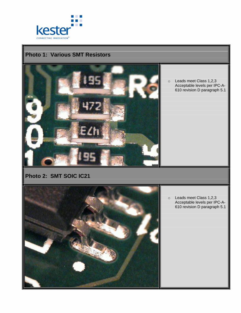
Photo 1: Various SMT Resistors
o Leads meet Class 1,2,3 Acceptable levels per IPC-A-610 revision D paragraph 5.1
Photo 2: SMT SOIC IC21
o Leads meet Class 1,2,3 Acceptable levels per IPC-A-610 revision D paragraph 5.1
Photo 3: SMT QFP IC14
o Leads meet Class 1,2,3 Acceptable levels per IPC-A-610 revision D paragraph 5.1
o Exposed basis metal common with lead free alloys and is acceptable per IPC-A-610 revision D paragraph 5.2.1.
Photo 4: SMT Resistor Network R70
o Leads meet Class 1,2,3 Acceptable levels per IPC-A-610 revision D paragraph 5.1
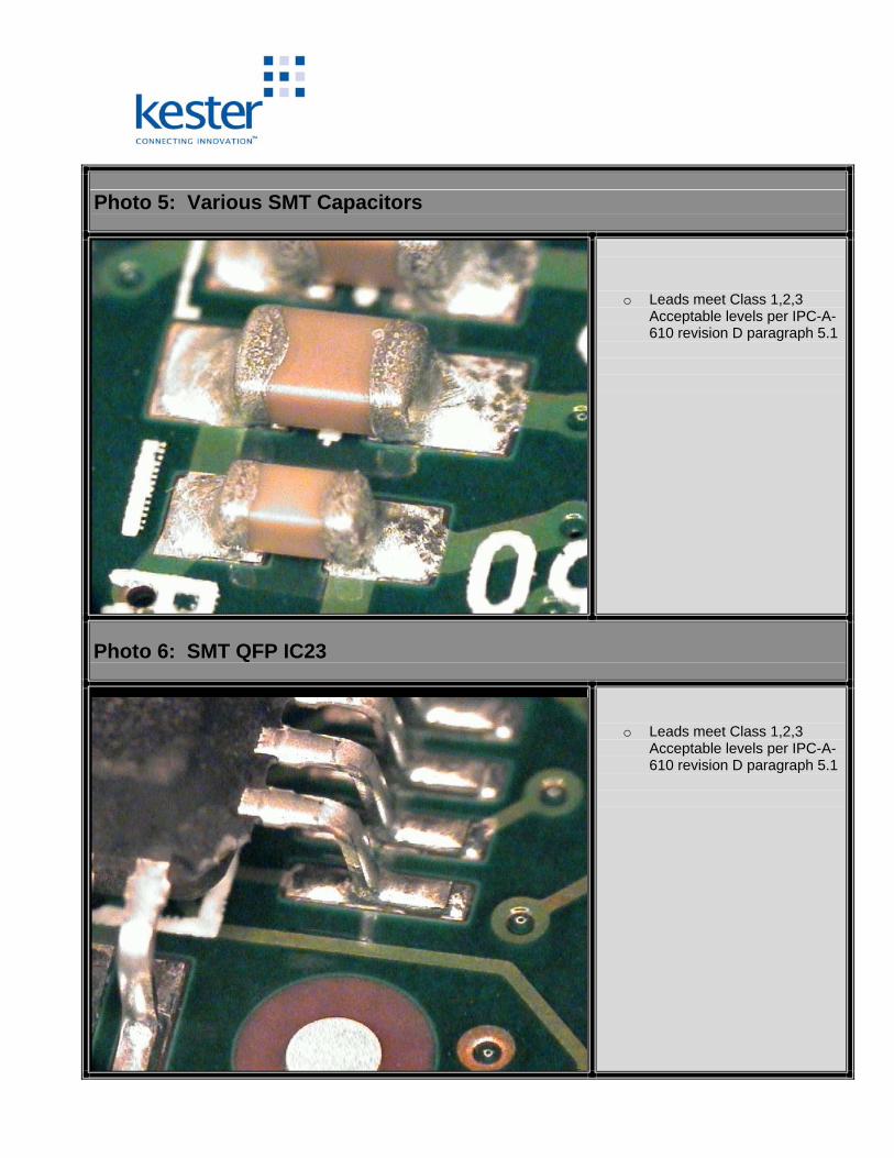
Photo 5: Various SMT Capacitors
o Leads meet Class 1,2,3 Acceptable levels per IPC-A-610 revision D paragraph 5.1
Photo 6: SMT QFP IC23
o Leads meet Class 1,2,3 Acceptable levels per IPC-A-610 revision D paragraph 5.1
Photo 7: SMT DIP J-Lead IC1
o Leads meet Class 1,2,3 Acceptable levels per IPC-A-610 revision D paragraph 5.1
Photo 8: Through Hole DIP IC19
o Leads meet Class 1,2,3 targets per IPC-A-610 revision D paragraph 7.5.5
o No void areas or surface imperfections.
o Leads and lands are well wetted.
o Leads are discernible. o 100% fillet around leads. o Solder covers lead and
feathers out to a thin edge on land.
o No evidence of fillet lifting.
Photo 9: Through Hole DIP IC12 Top Side
o There is 100% vertical hole fill.
o Vertical hole fill meets class 3 requirements per IPC-A-610 revision D paragraph 7.5.5 Table 7-6.
Photo 10: Through Hole DIP IC12 Bottom Side
o Leads meet Class 1,2,3 targets per IPC-A-610 revision D paragraph 7.5.5
o No void areas or surface imperfections.
o Leads and lands are well wetted.
o Leads are discernible. o 100% fillet around leads. o Solder covers lead and
feathers out to a thin edge on land.
o No evidence of fillet lifting.
Photo 11: Through Hole DIP IC17 Top Side
o There is 100% vertical hole fill.
o Vertical hole fill meets class 3 requirements per IPC-A-610 revision D paragraph 7.5.5 Table 7-6.
Photo 12: Through Hole DIP IC17 Bottom Side
o Leads meet Class 1,2,3 targets per IPC-A-610 revision D paragraph 7.5.5
o No void areas or surface imperfections.
o Leads and lands are well wetted.
o Leads are discernible. o 100% fillet around leads. o Solder covers lead and
feathers out to a thin edge on land.
o No evidence of fillet lifting.
Photo 13: Through Hole SIP Connector U11 Top Side
o There is 100% vertical hole fill.
o Vertical hole fill meets class 3 requirements per IPC-A-610 revision D paragraph 7.5.5 Table 7-6.
Photo 14: Through Hole SIP Connector U11 Bottom Side
o Leads meet Class 1,2,3 targets per IPC-A-610 revision D paragraph 7.5.5
o No void areas or surface imperfections.
o Leads and lands are well wetted.
o Leads are discernible. o 100% fillet around leads. o Solder covers lead and
feathers out to a thin edge on land.
o No evidence of fillet lifting.
Photo 15: Through Hole Terminal T2 Top Side
o There is 100% vertical hole fill.
o Vertical hole fill meets class 3 requirements per IPC-A-610 revision D paragraph 7.5.5 Table 7-6.
Photo 16: Through Hole Terminal T2 Bottom Side
o Leads meet Class 1,2,3 targets per IPC-A-610 revision D paragraph 7.5.5
o No void areas or surface imperfections.
o Leads and lands are well wetted.
o Leads are discernible. o 100% fillet around leads. o Solder covers lead and
feathers out to a thin edge on land.
o No evidence of fillet lifting.
Photo 17: Through Hole DIP IC15 Top Side
o There is 100% vertical hole fill.
o Vertical hole fill meets class 3 requirements per IPC-A-610 revision D paragraph 7.5.5 Table 7-6.
Photo 18: Through Hole DIP IC15 Bottom Side
o Leads meet Class 1,2,3 targets per IPC-A-610 revision D paragraph 7.5.5
o No void areas or surface imperfections.
o Leads and lands are well wetted.
o Leads are discernible. o 100% fillet around leads. o Solder covers lead and
feathers out to a thin edge on land.
o No evidence of fillet lifting.
Lead-free Validation Conclusions: • The lead-free assembly met customer expectations with the use of K100 alloy, R520A solder paste, 2235 liquid flux and K100 wire with 331 core flux. • Both SMD and Through-hole parts exhibited exceptional wetting characteristics
and excellent intermetallic formation. • Low voiding was observed in all types of lead-free joints. • Low contact angles were observed on SMD joints. • 100% vertical hole-fill was observed with all through-hole joints. • Wave soldering process optimization with the K100 Ultra-Pure solder was no
different than traditional leaded systems. • Kester 2235 liquid flux offered excellent activity on all components. • K100 solder wire with 331 core flux provided good wetting of soldered
components with no icicling or cold solder joints detected. No additional liquid flux was required for hand soldering. Joints assembled with K100 wire solder were smooth and bright.
• K100 wave soldered joints were as bright as Sn63Pb37 joints. • Cosmetics for R520A SAC305 solder paste were excellent, but less shiny than
the wave soldered joints. • The solder connections met or exceeded Class 1,2,3 per IPC-A-610 revision D
Paragraph 5.1. • No discoloration of components or boards was noticed at the optimized
temperatures used in all lead-free operations. A final word from SMT Dynamics, Anaheim, California. "As a contract manufacturer of high reliability products, we used K100 in our lead-free wave process and found excellent hole-fill, bright joints, free of defects. In the hand-soldering operation we used K100 solder wire, this gave us the same great results and the R520A solder paste gave us a problem free SMT process. We maintain the same quality and yields in our lead-free processes as our leaded process." Carlos Rivas, Director of Operations, SMT Dynamics, Anaheim, CA.