5-1 FAST AND LS TTL DATA QUAD 2-INPUT NOR GATE 14 13 12 11 10 9 1 2 3 4 5 6 V CC 8 7 GND GUARANTEED OPERATING RANGES Symbol Parameter Min Typ Max Unit V CC Supply Voltage 54 74 4.5 4.75 5.0 5.0 5.5 5.25 V T A Operating Ambient Temperature Range 54 74 –55 0 25 25 125 70 °C I OH Output Current — High 54, 74 – 0.4 mA I OL Output Current — Low 54 74 4.0 8.0 mA SN54/74LS02 QUAD 2-INPUT NOR GATE LOW POWER SCHOTTKY J SUFFIX CERAMIC CASE 632-08 N SUFFIX PLASTIC CASE 646-06 14 1 14 1 ORDERING INFORMATION SN54LSXXJ Ceramic SN74LSXXN Plastic SN74LSXXD SOIC 14 1 D SUFFIX SOIC CASE 751A-02
Transcript
5-1
FAST AND LS TTL DATA
QUAD 2-INPUT NOR GATE
14 13 12 11 10 9
1 2 3 4 5 6
VCC
8
7
GND
GUARANTEED OPERATING RANGES
Symbol Parameter Min Typ Max Unit
VCC Supply Voltage 5474
4.54.75
5.05.0
5.55.25
V
TA Operating Ambient Temperature Range 5474
–550
2525
12570
°C
IOH Output Current — High 54, 74 –0.4 mA
IOL Output Current — Low 5474
4.08.0
mA
SN54/74LS02
QUAD 2-INPUT NOR GATE
LOW POWER SCHOTTKY
J SUFFIXCERAMIC
CASE 632-08
N SUFFIXPLASTIC
CASE 646-06
141
14
1
ORDERING INFORMATION
SN54LSXXJ CeramicSN74LSXXN PlasticSN74LSXXD SOIC
141
D SUFFIXSOIC
CASE 751A-02
5-2
FAST AND LS TTL DATA
SN54/74LS02
DC CHARACTERISTICS OVER OPERATING TEMPERATURE RANGE (unless otherwise specified)
S b l P
Limits
U i T C di iSymbol Parameter Min Typ Max Unit Test Conditions
VIH Input HIGH Voltage 2.0 VGuaranteed Input HIGH Voltage forAll Inputs
VIL Input LOW Voltage54 0.7
VGuaranteed Input LOW Voltage for
VIL Input LOW Voltage74 0.8
Vp g
All Inputs
VIK Input Clamp Diode Voltage –0.65 –1.5 V VCC = MIN, IIN = –18 mA
VOH Output HIGH Voltage54 2.5 3.5 V VCC = MIN, IOH = MAX, VIN = VIHVOH Output HIGH Voltage74 2.7 3.5 V
CC , OH , IN IHor VIL per Truth Table
VOL Output LOW Voltage54, 74 0.25 0.4 V IOL = 4.0 mA VCC = VCC MIN,
VIN = VIL or VIHVOL Output LOW Voltage74 0.35 0.5 V IOL = 8.0 mA
VIN = VIL or VIHper Truth Table
IIH Input HIGH Current20 µA VCC = MAX, VIN = 2.7 V
IIH Input HIGH Current0.1 mA VCC = MAX, VIN = 7.0 V
IIL Input LOW Current –0.4 mA VCC = MAX, VIN = 0.4 V
IOS Short Circuit Current (Note 1) –20 –100 mA VCC = MAX
ICC
Power Supply CurrentTotal, Output HIGH 3.2 mA VCC = MAXICCTotal, Output LOW 5.4
mA VCC MAX
Note 1: Not more than one output should be shorted at a time, nor for more than 1 second.
AC CHARACTERISTICS (TA = 25°C)
S b l P
Limits
U i T C di iSymbol Parameter Min Typ Max Unit Test Conditions
tPLH Turn-Off Delay, Input to Output 10 15 ns VCC = 5.0 V
tPHL Turn-On Delay, Input to Output 10 15 nsCC
CL = 15 pF
5-1
FAST AND LS TTL DATA
HEX INVERTER
14 13 12 11 10 9
1 2 3 4 5 6
VCC
8
7
GND
* * *
* * *
* OPEN COLLECTOR OUTPUTS
GUARANTEED OPERATING RANGES
Symbol Parameter Min Typ Max Unit
VCC Supply Voltage 5474
4.54.75
5.05.0
5.55.25
V
TA Operating Ambient Temperature Range 5474
–550
2525
12570
°C
VOH Output Voltage — High 54, 74 5.5 V
IOL Output Current — Low 5474
4.08.0
mA
SN54/74LS05
HEX INVERTER
LOW POWER SCHOTTKY
J SUFFIXCERAMIC
CASE 632-08
N SUFFIXPLASTIC
CASE 646-06
141
14
1
ORDERING INFORMATION
SN54LSXXJ CeramicSN74LSXXN PlasticSN74LSXXD SOIC
141
D SUFFIXSOIC
CASE 751A-02
5-2
FAST AND LS TTL DATA
SN54/74LS05
DC CHARACTERISTICS OVER OPERATING TEMPERATURE RANGE (unless otherwise specified)
S b l P
Limits
U i T C di iSymbol Parameter Min Typ Max Unit Test Conditions
VIH Input HIGH Voltage 2.0 VGuaranteed Input HIGH Voltage forAll Inputs
VIL Input LOW Voltage54 0.7
VGuaranteed Input LOW Voltage for
VIL Input LOW Voltage74 0.8
Vp g
All Inputs
VIK Input Clamp Diode Voltage –0.65 –1.5 V VCC = MIN, IIN = –18 mA
IOH Output HIGH Current 54, 74 100 µA VCC = MIN, VOH = MAX
VOL Output LOW Voltage54, 74 0.25 0.4 V IOL = 4.0 mA VCC = VCC MIN,
VIN = VIL or VIHVOL Output LOW Voltage74 0.35 0.5 V IOL = 8.0 mA
VIN = VIL or VIHper Truth Table
IIH Input HIGH Current20 µA VCC = MAX, VIN = 2.7 V
IIH Input HIGH Current0.1 mA VCC = MAX, VIN = 7.0 V
IIL Input LOW Current –0.4 mA VCC = MAX, VIN = 0.4 V
ICC
Power Supply CurrentTotal, Output HIGH 2.4 mA VCC = MAXICCTotal, Output LOW 6.6
mA VCC MAX
AC CHARACTERISTICS (TA = 25°C)
S b l P
Limits
U i T C di iSymbol Parameter Min Typ Max Unit Test Conditions
tPLH Turn-Off Delay, Input to Output 17 32 ns VCC = 5.0 V
tPHL Turn-On Delay, Input to Output 15 28 nsCC
CL = 15 pF, RL = 2.0 kΩ
5-1
FAST AND LS TTL DATA
QUAD 2-INPUT AND GATE
14 13 12 11 10 9
1 2 3 4 5 6
VCC
8
7
GND
GUARANTEED OPERATING RANGES
Symbol Parameter Min Typ Max Unit
VCC Supply Voltage 5474
4.54.75
5.05.0
5.55.25
V
TA Operating Ambient Temperature Range 5474
–550
2525
12570
°C
IOH Output Current — High 54, 74 –0.4 mA
IOL Output Current — Low 5474
4.08.0
mA
SN54/74LS08
QUAD 2-INPUT AND GATE
LOW POWER SCHOTTKY
J SUFFIXCERAMIC
CASE 632-08
N SUFFIXPLASTIC
CASE 646-06
141
14
1
ORDERING INFORMATION
SN54LSXXJ CeramicSN74LSXXN PlasticSN74LSXXD SOIC
141
D SUFFIXSOIC
CASE 751A-02
5-2
FAST AND LS TTL DATA
SN54/74LS08
DC CHARACTERISTICS OVER OPERATING TEMPERATURE RANGE (unless otherwise specified)
S b l P
Limits
U i T C di iSymbol Parameter Min Typ Max Unit Test Conditions
VIH Input HIGH Voltage 2.0 VGuaranteed Input HIGH Voltage forAll Inputs
VIL Input LOW Voltage54 0.7
VGuaranteed Input LOW Voltage for
VIL Input LOW Voltage74 0.8
Vp g
All Inputs
VIK Input Clamp Diode Voltage –0.65 –1.5 V VCC = MIN, IIN = –18 mA
VOH Output HIGH Voltage54 2.5 3.5 V VCC = MIN, IOH = MAX, VIN = VIHVOH Output HIGH Voltage74 2.7 3.5 V
CC , OH , IN IHor VIL per Truth Table
VOL Output LOW Voltage54, 74 0.25 0.4 V IOL = 4.0 mA VCC = VCC MIN,
VIN = VIL or VIHVOL Output LOW Voltage74 0.35 0.5 V IOL = 8.0 mA
VIN = VIL or VIHper Truth Table
IIH Input HIGH Current20 µA VCC = MAX, VIN = 2.7 V
IIH Input HIGH Current0.1 mA VCC = MAX, VIN = 7.0 V
IIL Input LOW Current –0.4 mA VCC = MAX, VIN = 0.4 V
IOS Short Circuit Current (Note 1) –20 –100 mA VCC = MAX
ICC
Power Supply CurrentTotal, Output HIGH 4.8 mA VCC = MAXICCTotal, Output LOW 8.8
mA VCC MAX
Note 1: Not more than one output should be shorted at a time, nor for more than 1 second.
AC CHARACTERISTICS (TA = 25°C)
S b l P
Limits
U i T C di iSymbol Parameter Min Typ Max Unit Test Conditions
tPLH Turn-Off Delay, Input to Output 8.0 15 ns VCC = 5.0 V
tPHL Turn-On Delay, Input to Output 10 20 nsCC
CL = 15 pF
5-1
FAST AND LS TTL DATA
TRIPLE 3-INPUT NAND GATE
14 13 12 11 10 9
1 2 3 4 5 6
VCC
8
7
GND
GUARANTEED OPERATING RANGES
Symbol Parameter Min Typ Max Unit
VCC Supply Voltage 5474
4.54.75
5.05.0
5.55.25
V
TA Operating Ambient Temperature Range 5474
–550
2525
12570
°C
IOH Output Current — High 54, 74 –0.4 mA
IOL Output Current — Low 5474
4.08.0
mA
SN54/74LS10
TRIPLE 3-INPUT NAND GATE
LOW POWER SCHOTTKY
J SUFFIXCERAMIC
CASE 632-08
N SUFFIXPLASTIC
CASE 646-06
141
14
1
ORDERING INFORMATION
SN54LSXXJ CeramicSN74LSXXN PlasticSN74LSXXD SOIC
141
D SUFFIXSOIC
CASE 751A-02
5-2
FAST AND LS TTL DATA
SN54/74LS10
DC CHARACTERISTICS OVER OPERATING TEMPERATURE RANGE (unless otherwise specified)
S b l P
Limits
U i T C di iSymbol Parameter Min Typ Max Unit Test Conditions
VIH Input HIGH Voltage 2.0 VGuaranteed Input HIGH Voltage forAll Inputs
VIL Input LOW Voltage54 0.7
VGuaranteed Input LOW Voltage for
VIL Input LOW Voltage74 0.8
Vp g
All Inputs
VIK Input Clamp Diode Voltage –0.65 –1.5 V VCC = MIN, IIN = –18 mA
VOH Output HIGH Voltage54 2.5 3.5 V VCC = MIN, IOH = MAX, VIN = VIHVOH Output HIGH Voltage74 2.7 3.5 V
CC , OH , IN IHor VIL per Truth Table
VOL Output LOW Voltage54, 74 0.25 0.4 V IOL = 4.0 mA VCC = VCC MIN,
VIN = VIL or VIHVOL Output LOW Voltage74 0.35 0.5 V IOL = 8.0 mA
VIN = VIL or VIHper Truth Table
IIH Input HIGH Current20 µA VCC = MAX, VIN = 2.7 V
IIH Input HIGH Current0.1 mA VCC = MAX, VIN = 7.0 V
IIL Input LOW Current –0.4 mA VCC = MAX, VIN = 0.4 V
IOS Short Circuit Current (Note 1) –20 –100 mA VCC = MAX
ICC
Power Supply CurrentTotal, Output HIGH 1.2 mA VCC = MAXICC p
Total, Output LOW 3.3
mA VCC MAX
Note 1: Not more than one output should be shorted at a time, nor for more than 1 second.
AC CHARACTERISTICS (TA = 25°C)
S b l P
Limits
U i T C di iSymbol Parameter Min Typ Max Unit Test Conditions
tPLH Turn-Off Delay, Input to Output 9.0 15 ns VCC = 5.0 V
tPHL Turn-On Delay, Input to Output 10 15 nsCC
CL = 15 pF
5-1
FAST AND LS TTL DATA
SCHMITT TRIGGERSDUAL GATE/HEX INVERTER
The SN54LS/74LS13 and SN54LS/74LS14 contain logic gates/ inverterswhich accept standard TTL input signals and provide standard TTL outputlevels. They are capable of transforming slowly changing input signals intosharply defined, jitter-free output signals. Additionally, they have greater noisemargin than conventional inverters.
Each circuit contains a Schmitt trigger followed by a Darlington level shifterand a phase splitter driving a TTL totem pole output. The Schmitt trigger usespositive feedback to effectively speed-up slow input transitions, and providedifferent input threshold voltages for positive and negative-going transitions.This hysteresis between the positive-going and negative-going inputthresholds (typically 800 mV) is determined internally by resistor ratios and isessentially insensitive to temperature and supply voltage variations.
14 13 12 11 10 9
1 2 3 4 5 6
VCC
8
7
GND
LOGIC AND CONNECTION DIAGRAMS
SN54/74LS13
SN54/74LS14
14 13 12 11 10 9
1 2 3 4 5 6
VCC
8
7
GND
GUARANTEED OPERATING RANGES
Symbol Parameter Min Typ Max Unit
VCC Supply Voltage 5474
4.54.75
5.05.0
5.55.25
V
TA Operating Ambient Temperature Range 5474
–550
2525
12570
°C
IOH Output Current — High 54, 74 –0.4 mA
IOL Output Current — Low 5474
4.08.0
mA
SN54/74LS13SN54/74LS14
SCHMITT TRIGGERSDUAL GATE/HEX INVERTER
LOW POWER SCHOTTKY
J SUFFIXCERAMIC
CASE 632-08
N SUFFIXPLASTIC
CASE 646-06
141
14
1
ORDERING INFORMATION
SN54LSXXJ CeramicSN74LSXXN PlasticSN74LSXXD SOIC
141
D SUFFIXSOIC
CASE 751A-02
5-2
FAST AND LS TTL DATA
SN54/74LS13 • SN54/74LS14
DC CHARACTERISTICS OVER OPERATING TEMPERATURE RANGE (unless otherwise specified)
S b l P
Limits
U i T C di iSymbol Parameter Min Typ Max Unit Test Conditions
VT+ Positive-Going Threshold Voltage 1.5 2.0 V VCC = 5.0 V
VT– Negative-Going Threshold Voltage 0.6 1.1 V VCC = 5.0 V
VT+–VT– Hysteresis 0.4 0.8 V VCC = 5.0 V
VIK Input Clamp Diode Voltage –0.65 –1.5 V VCC = MIN, IIN = –18 mA
VOH Output HIGH Voltage54 2.5 3.4 V
VCC = MIN IOH = –400 µA VIN = VILVOH Output HIGH Voltage74 2.7 3.4 V
VCC = MIN, IOH = –400 µA, VIN = VIL
VOL Output LOW Voltage54, 74 0.25 0.4 V VCC = MIN, IOL = 4.0 mA, VIN = 2.0 V
VOL Output LOW Voltage74 0.35 0.5 V VCC = MIN, IOL = 8.0 mA, VIN = 2.0 V
IT+ Input Current at Positive-Going Threshold –0.14 mA VCC = 5.0 V, VIN = VT+
IT– Input Current at Negative-Going Threshold –0.18 mA VCC = 5.0 V, VIN = VT–
IIH Input HIGH Current1.0 20 µA VCC = MAX, VIN = 2.7 V
IIH Input HIGH Current0.1 mA VCC = MAX, VIN = 7.0 V
IIL Input LOW Current –0.4 mA VCC = MAX, VIN = 0.4 V
IOS Short Circuit Current (Note 1) –20 –100 mA VCC = MAX, VOUT = 0 V
I
Power Supply Current
Total Output HIGHLS13 2.9 6.0
A V MAXICCTotal, Output HIGH
LS14 8.6 16 mA VCC = MAXCC
Total Output LOWLS13 4.1 7.0
CC
Total, Output LOWLS14 12 21
Note 1: Not more than one output should be shorted at a time, nor for more than 1 second.
AC CHARACTERISTICS (TA = 25°C)
S b l P
Max
U i T C di iSymbol Parameter LS13 LS14 Unit Test Conditions
tPLH Propagation Delay, Input to Output 22 22 ns VCC = 5.0 V
tPHL Propagation Delay, Input to Output 27 22 nsCC
CL = 15 pF
Figure 1. AC Waveforms
3 V
0 V
VIN
VOUT
1.6 V0.8 V
tPHL
1.3 V 1.3 V
tPLH
Figure 2. V IN versus V OUT Transfer Function
Figure 3. Threshold Voltage and Hysteresisversus Power Supply Voltage
Figure 4. Threshold Voltage Hysteresisversus Temperature
5
4
3
2
1
00 0.4 0.95 1.2 1.8 2
VIN, INPUT VOLTAGE (VOLTS)
VO
, OU
TPU
T VO
LTAG
E (V
OLT
S)
VCC = 5 VTA = 25°C
2
1.6
1.2
0.8
0.4
04.5 4.75 5 5.25 5.5
VCC, POWER SUPPLY VOLTAGE (VOLTS)
VT
, TH
RES
HO
LD V
OLT
AGE
(VO
LTS)
VT,
HYS
TER
ESIS
(VO
LTS)
∆
1.9
1.7
1.5
1.3
1.1
0.9
0.7– 55° 0° 25° 75° 125°
TA, AMBIENT TEMPERATURE (°C)
VT
, TH
RES
HO
LD V
OLT
AGE
(VO
LTS)
VT,
HYS
TER
ESIS
(VO
LTS)
∆
TA = 25°C
VT+
VT–
∆ VT
VT+
VT–
∆ VT
5-3
FAST AND LS TTL DATA
SN54/74LS13 • SN54/74LS14
SN54LS06, SN54LS16, SN74LS06, SN74LS16 HEX INVERTER BUFFERS/DRIVERS WITH
OPEN-COLLECTOR HIGH-VOLTAGE OUTPUTS SDLS020A – MAY 1990
Copyright 1990, Texas Instruments Incorporated
1POST OFFICE BOX 655303 • DALLAS, TEXAS 75265
• Converts TTL Voltage Levels to MOSLevels
• High Sink-Current Capability
• Input Clamping Diodes Simplify SystemDesign
• Open-Collector Driver for Indicator Lampsand Relays
• Package Options Include “Small Outline”Packages, Ceramic Chip Carriers, andStandard Plastic and Ceramic 300-mil DIPs
description
These monolithic hex inverter buffers/driversfeature high-voltage open-collector outputs tointerface with high-level circuits (such as MOS), orfor driving high-current loads, and are alsocharacterized for use as inverter buffers for drivingTTL inputs. The ′LS06 has a rated output voltageof 30 V and the ′LS16 has a rated output voltageof 15 V. The maximum sink current for theSN54LS06 and SN54LS16 is 30 mA and theSN74LS06 and SN74LS16 is 40 mA.
These circuits are compatible with most TTLfamilies. Inputs are diode-clamped to minimizetransmission-effects, which simplifies design.Typical power dissipation is 175 mW and averagepropagation delay time is 8 ns.
The SN54LS06 and SN54LS16 are characterized over the full military temperature range of –55°C to 125°C.The SN74LS06 and SN74LS16 are characterized for operation from 0°C to 70°C.
logic symbol † logic diagram (positive logic)
1Y211A
2Y4
3Y6
4Y8
5Y10
6Y12
32A53A94A115A136A
1A
2A
3A
4A
5A
6A
1Y
2Y
3Y
4Y
5Y
6Y
† This symbol is in accordance with ANSI/IEEE Std 91-1984 and IECPublication 617-12.
Pin numbers shown are for D, J, and N packages.
1
3
5
9
11
13
2
4
6
8
10
12
1
2
3
4
5
6
7
14
13
12
11
10
9
8
1A1Y2A2Y3A3Y
GND
VCC6A6Y5A5Y4A4Y
SN54LS06, SN54LS16 . . . J PACKAGESN74LS06, SN74LS16 . . . D OR N PACKAGE
(T0P VIEW)
3 2 1 20 19
9 10 11 12 13
4
5
6
7
8
18
17
16
15
14
6YNC5ANC5Y
2ANC2YNC3A
SN54LS06, SN54LS16 . . . FK PACKAGE(T0P VIEW)
1Y 1A NC
4Y 4A6A
3YG
ND
NC
NC – No internal connection
V CC
UNLESS OTHERWISE NOTED this document contains PRODUCTIONDATA information current as of publication date. Products conform tospecifications per the terms of Texas Instruments standard warranty.Production processing does not necessarily include testing of allparameters.
PRODUCT PREVIEW information concerns products in the formative ordesign phase of development. Characteristic data and otherspecifications are design goals. Texas Instruments reserves the right tochange or discontinue these products without notice.
† Stresses beyond those listed under “absolute maximum ratings” may cause permanent damage to the device. This are stress ratings only, andfunctional operation of the device at these or any other conditions beyond those indicated under “recommended operating conditions” is notimplied. Exposure to absolute-maximum-rated conditions for extended periods may affect device reliability.
NOTES: 1. Voltage values are with respect to network ground terminal.2. This is the maximum voltage that should be applied to any output when it is in the off state.
recommended operating conditions
SN54LS06 SN74LS06
SN54LS16 SN74LS16 UNIT
MIN NOM MAX MIN NOM MAX
VCC Supply voltage 4.5 5 5.5 4.75 5 5.25 V
VIH High-level input voltage 2 2 V
VIL Low-level input voltage 0.8 0.8 V
’LS06 30 30
’LS16 15 15
IOL Low-level output current 30 40 mA
TA Operating free-air temperature –55 125 0 70 °C
IOH VCC = MIN, VIL = 0.8 V mA
PARAMETER TEST CONDITIONS MIN TYP MAX UNIT
A Y RL = 110 Ω, CL = 15 pF ns
PRODUCT PREVIEW information concerns products inthe formative or design phase of development.Characteristic data and other specifications are designgoals. Texas Instruments reserves the right to change ordiscontinue these products without notice.
SN54LS06, SN54LS16, SN74LS06, SN74LS16 HEX INVERTER BUFFERS/DRIVERS WITH
OPEN-COLLECTOR HIGH-VOLTAGE OUTPUTS SDLS020A – MAY 1990
3POST OFFICE BOX 655303 • DALLAS, TEXAS 75265
electrical characteristics over recommended operating free-air temperature range (unlessotherwise noted)
SN54LS06 SN74LS06
PARAMETER TEST CONDITIONS† SN54LS16 SN74LS16 UNIT
MIN TYP‡ MAX MIN TYP‡ MAX
VIK VCC = MIN, II = –12 mA –1.5 –1.5 V
’LS06, VOH = 30 V 0.25 0.25
’LS16, VOH = 15 V 0.25 0.25
IOL = 16 mA 0.25 0.4 0.25 0.4
VOL VCC = MIN, VIH = 2 V IOL = 30 mA 0.7 V
IOL = 40 mA 0.7
II VCC = MAX, VI = 7 V 1 1 mA
IIH VCC = MAX, VI = 2.4 V 20 20 µA
IIL VCC =MAX, VI = 0.4 V –0.2 –0.2 mA
ICCH VCC = MAX 18 18 mA
ICCL VCC = MAX 60 60 mA† For conditions shown as MIN or MAX, use the appropriate value specified under recommended operating conditions.‡ All typical values are at VCC = 5 V, and TA = 25°C.
switching characteristics, V CC = 5 V, TA = 25°C (see Note 3)
FROM TO
(INPUT) (OUTPUT)
tPLH 7 15
tPHL 10 20
NOTE 3: Load circuit and voltage waveforms are shown in Section 1 of TTL Logic Data Book, 1988.
IMPORTANT NOTICE
Texas Instruments (TI) reserves the right to make changes to its products or to discontinue any semiconductorproduct or service without notice, and advises its customers to obtain the latest version of relevant informationto verify, before placing orders, that the information being relied on is current.
TI warrants performance of its semiconductor products and related software to the specifications applicable atthe time of sale in accordance with TI’s standard warranty. Testing and other quality control techniques areutilized to the extent TI deems necessary to support this warranty. Specific testing of all parameters of eachdevice is not necessarily performed, except those mandated by government requirements.
Certain applications using semiconductor products may involve potential risks of death, personal injury, orsevere property or environmental damage (“Critical Applications”).
TI SEMICONDUCTOR PRODUCTS ARE NOT DESIGNED, INTENDED, AUTHORIZED, OR WARRANTEDTO BE SUITABLE FOR USE IN LIFE-SUPPORT APPLICATIONS, DEVICES OR SYSTEMS OR OTHERCRITICAL APPLICATIONS.
Inclusion of TI products in such applications is understood to be fully at the risk of the customer. Use of TIproducts in such applications requires the written approval of an appropriate TI officer. Questions concerningpotential risk applications should be directed to TI through a local SC sales office.
In order to minimize risks associated with the customer’s applications, adequate design and operatingsafeguards should be provided by the customer to minimize inherent or procedural hazards.
TI assumes no liability for applications assistance, customer product design, software performance, orinfringement of patents or services described herein. Nor does TI warrant or represent that any license, eitherexpress or implied, is granted under any patent right, copyright, mask work right, or other intellectual propertyright of TI covering or relating to any combination, machine, or process in which such semiconductor productsor services might be or are used.
Copyright 1995, Texas Instruments Incorporated
SN54LS07, SN74LS07, SN74LS17HEX BUFFERS/DRIVERS WITH
OPEN-COLLECTOR HIGH-VOLTAGE OUTPUTSSDLS021A, D3517, MAY 1990–REVISED AUGUST 1991
POST OFFICE BOX 655303 • DALLAS, TEXAS 75265
Copyright 1991, Texas Instruments Incorporated
1
PRODUCTION DATA information is current as of publication date.Products conform to specifications per the terms of TexasInstruments standard warranty. Production processing does notnecessarily include testing of all parameters.
• Converts TTL-Voltage Levels to MOSLevels
• High Sink-Current Capability
• Input Clamping Diodes Simplify SystemDesign
• Open-Collector Driver for Indicator Lampsand Relays
• Package Options Include “Small Outline”Packages, Ceramic Chip Carriers, andStandard and Ceramic 300-mil DIPs
description
These monolithic hex buffers/drivers featurehigh-voltage open-collector outputs to interfacewith high-level circuits or for driving high-currentloads. They are also characterized for use asbuffers for driving TTL inputs. The ′LS07 has arated output voltage of 30 V and the ′LS17 has arated output voltage of 15 V. The maximum sinkcurrent is 30 mA for the SN54LS07 and 40 mA forthe SN74LS07 and SN74LS17.
These circuits are compatible with most TTLfamilies. Inputs are diode-clamped to minimizetransmission-line effects, which simplifies design.Typical power dissipation is 140 mW and averagepropagation delay time is 12 ns.
The SN54LS07 is characterized over the full military temperature range of –55°C to 125°C. The SN74LS07 andSN74LS17 are characterized for operation from 0°C to 70°C.
logic symbol † logic diagram (positive logic)
1Y211A
2Y4
3Y6
4Y8
5Y10
6Y12
32A53A94A115A136A
1A
2A
3A
4A
5A
6A
1Y
2Y
3Y
4Y
5Y
6Y
† This symbol is in accordance with ANSI/IEEE Std 91-1984 andIEC Publication 617-12.
Pin numbers shown are for D, J, and N packages.
1
3
5
9
11
13
2
4
6
8
10
12
1
2
3
4
5
6
7
14
13
12
11
10
9
8
1A1Y2A2Y3A3Y
GND
VCC6A6Y5A5Y4A4Y
SN54LS07 . . . J PACKAGESN74LS07, SN74LS17 . . . D OR N PACKAGE
† Stresses beyond those listed under “absolute maximum ratings” may cause permanent damage to the device. These are stress ratings only, andfunctional operation of the device at these or any other conditions beyond those indicated under “recommended operating conditions” is notimplied. Exposure to absolute-maximum-rated conditions for extended periods may affect device reliability.
NOTES: 1. Voltage values are with respect to network ground terminal.2. This is the maximum voltage that should be applied to any output when it is in the off state.
recommended operating conditions
SN74LS07
SN74LS17 UNIT
MIN NOM MAX MIN NOM MAX
VCC Supply voltage 4.5 5 5.5 4.75 5 5.25 V
VIH High-level input voltage 2 2 V
VIL Low-level input voltage 0.8 0.8 V
’LS07 30 30
’LS17 15
IOL Low-level output current 30 40 mA
TA Operating free-air temperature –55 125 0 70 °C
IOH
VOL
VCC = MIN,
VIL = 0.8 VVCC = MIN,
VIH = 2 V
V
mA
SN54LS07
PARAMETER TEST CONDITIONS MIN TYP MAX UNIT
A Y RL = 110 Ω, CL = 15 pF ns
SN54LS07, SN74LS07, SN74LS17HEX BUFFERS/DRIVERS WITH
OPEN-COLLECTOR HIGH-VOLTAGE OUTPUTS
POST OFFICE BOX 655303 • DALLAS, TEXAS 75265 3
electrical characteristics over recommended operating free-air temperature range (unlessotherwise noted)
SN74LS07
PARAMETER TEST CONDITIONS† SN74LS17 UNIT
MIN TYP‡ MAX MIN TYP‡ MAX
VIK VCC = MIN, II = –12 mA –1.5 –1.5 V
’LS07, VOH = 30 V 0.25 0.25
’LS17, VOH = 15 V 0.25 0.25
IOL = 16 mA 0.4 0.4
IOL = MAX§ 0.7 0.7
II VCC = MAX, VI = 7 V 1 1 mA
IIH VCC = MAX, VI = 2.4 V 20 20 µA
IIL VCC = MAX, VI = 0.4 V –0.2 –0.2 mA
ICCH VCC = MAX 14 14 mA
ICCL VCC = MAX 45 45 mA† For conditions shown as MIN or MAX, use the appropriate value specified under recommended operating conditions.‡ All typical values are at VCC = 5 V, TA = 25°C.§ IOL = 30 mA for SN54 series parts and 40 mA for SN74 series parts.
switching characteristics, V CC = 5 V, TA = 25°C (see Note 3)
FROM TO
(INPUT) (OUTPUT)
tPLH 6 10
tPHL 19 30
NOTE 3: Load circuit and voltage waveforms are shown in Section 1 of TTL Logic Data Book, 1988.
IMPORTANT NOTICE
Texas Instruments (TI) reserves the right to make changes to its products or to discontinue any semiconductorproduct or service without notice, and advises its customers to obtain the latest version of relevant informationto verify, before placing orders, that the information being relied on is current.
TI warrants performance of its semiconductor products and related software to the specifications applicable atthe time of sale in accordance with TI’s standard warranty. Testing and other quality control techniques areutilized to the extent TI deems necessary to support this warranty. Specific testing of all parameters of eachdevice is not necessarily performed, except those mandated by government requirements.
Certain applications using semiconductor products may involve potential risks of death, personal injury, orsevere property or environmental damage (“Critical Applications”).
TI SEMICONDUCTOR PRODUCTS ARE NOT DESIGNED, INTENDED, AUTHORIZED, OR WARRANTEDTO BE SUITABLE FOR USE IN LIFE-SUPPORT APPLICATIONS, DEVICES OR SYSTEMS OR OTHERCRITICAL APPLICATIONS.
Inclusion of TI products in such applications is understood to be fully at the risk of the customer. Use of TIproducts in such applications requires the written approval of an appropriate TI officer. Questions concerningpotential risk applications should be directed to TI through a local SC sales office.
In order to minimize risks associated with the customer’s applications, adequate design and operatingsafeguards should be provided by the customer to minimize inherent or procedural hazards.
TI assumes no liability for applications assistance, customer product design, software performance, orinfringement of patents or services described herein. Nor does TI warrant or represent that any license, eitherexpress or implied, is granted under any patent right, copyright, mask work right, or other intellectual propertyright of TI covering or relating to any combination, machine, or process in which such semiconductor productsor services might be or are used.
Copyright 1995, Texas Instruments Incorporated
5-1
FAST AND LS TTL DATA
DUAL 4-INPUT NAND GATE
14 13 12 11 10 9
1 2 3 4 5 6
VCC
8
7
GND
GUARANTEED OPERATING RANGES
Symbol Parameter Min Typ Max Unit
VCC Supply Voltage 5474
4.54.75
5.05.0
5.55.25
V
TA Operating Ambient Temperature Range 5474
–550
2525
12570
°C
IOH Output Current — High 54, 74 –0.4 mA
IOL Output Current — Low 5474
4.08.0
mA
SN54/74LS20
DUAL 4-INPUT NAND GATE
LOW POWER SCHOTTKY
J SUFFIXCERAMIC
CASE 632-08
N SUFFIXPLASTIC
CASE 646-06
141
14
1
ORDERING INFORMATION
SN54LSXXJ CeramicSN74LSXXN PlasticSN74LSXXD SOIC
141
D SUFFIXSOIC
CASE 751A-02
5-2
FAST AND LS TTL DATA
SN54/74LS20
DC CHARACTERISTICS OVER OPERATING TEMPERATURE RANGE (unless otherwise specified)
S b l P
Limits
U i T C di iSymbol Parameter Min Typ Max Unit Test Conditions
VIH Input HIGH Voltage 2.0 VGuaranteed Input HIGH Voltage forAll Inputs
VIL Input LOW Voltage54 0.7
VGuaranteed Input LOW Voltage for
VIL Input LOW Voltage74 0.8
Vp g
All Inputs
VIK Input Clamp Diode Voltage –0.65 –1.5 V VCC = MIN, IIN = –18 mA
VOH Output HIGH Voltage54 2.5 3.5 V VCC = MIN, IOH = MAX, VIN = VIHVOH Output HIGH Voltage74 2.7 3.5 V
CC , OH , IN IHor VIL per Truth Table
VOL Output LOW Voltage54, 74 0.25 0.4 V IOL = 4.0 mA VCC = VCC MIN,
VIN = VIL or VIHVOL Output LOW Voltage74 0.35 0.5 V IOL = 8.0 mA
VIN = VIL or VIHper Truth Table
IIH Input HIGH Current20 µA VCC = MAX, VIN = 2.7 V
IIH Input HIGH Current0.1 mA VCC = MAX, VIN = 7.0 V
IIL Input LOW Current –0.4 mA VCC = MAX, VIN = 0.4 V
IOS Short Circuit Current (Note 1) –20 –100 mA VCC = MAX
ICC
Power Supply CurrentTotal, Output HIGH 0.8 mA VCC = MAXICC p
Total, Output LOW 2.2
mA VCC MAX
Note 1: Not more than one output should be shorted at a time, nor for more than 1 second.
AC CHARACTERISTICS (TA = 25°C)
S b l P
Limits
U i T C di iSymbol Parameter Min Typ Max Unit Test Conditions
tPLH Turn-Off Delay, Input to Output 9.0 15 ns VCC = 5.0 V
tPHL Turn-On Delay, Input to Output 10 15 nsCC
CL = 15 pF
5-1
FAST AND LS TTL DATA
8-INPUT NAND GATE
14 13 12 11 10 9
1 2 3 4 5 6
VCC
8
7
GND
GUARANTEED OPERATING RANGES
Symbol Parameter Min Typ Max Unit
VCC Supply Voltage 5474
4.54.75
5.05.0
5.55.25
V
TA Operating Ambient Temperature Range 5474
–550
2525
12570
°C
IOH Output Current — High 54, 74 –0.4 mA
IOL Output Current — Low 5474
4.08.0
mA
SN54/74LS30
8-INPUT NAND GATE
LOW POWER SCHOTTKY
J SUFFIXCERAMIC
CASE 632-08
N SUFFIXPLASTIC
CASE 646-06
141
14
1
ORDERING INFORMATION
SN54LSXXJ CeramicSN74LSXXN PlasticSN74LSXXD SOIC
141
D SUFFIXSOIC
CASE 751A-02
5-2
FAST AND LS TTL DATA
SN54/74LS30
DC CHARACTERISTICS OVER OPERATING TEMPERATURE RANGE (unless otherwise specified)
S b l P
Limits
U i T C di iSymbol Parameter Min Typ Max Unit Test Conditions
VIH Input HIGH Voltage 2.0 VGuaranteed Input HIGH Voltage forAll Inputs
VIL Input LOW Voltage54 0.7
VGuaranteed Input LOW Voltage for
VIL Input LOW Voltage74 0.8
Vp g
All Inputs
VIK Input Clamp Diode Voltage –0.65 –1.5 V VCC = MIN, IIN = –18 mA
VOH Output HIGH Voltage54 2.5 3.5 V VCC = MIN, IOH = MAX, VIN = VIHVOH Output HIGH Voltage74 2.7 3.5 V
CC , OH , IN IHor VIL per Truth Table
VOL Output LOW Voltage54, 74 0.25 0.4 V IOL = 4.0 mA VCC = VCC MIN,
VIN = VIL or VIHVOL Output LOW Voltage74 0.35 0.5 V IOL = 8.0 mA
VIN = VIL or VIHper Truth Table
IIH Input HIGH Current20 µA VCC = MAX, VIN = 2.7 V
IIH Input HIGH Current0.1 mA VCC = MAX, VIN = 7.0 V
IIL Input LOW Current –0.4 mA VCC = MAX, VIN = 0.4 V
IOS Short Circuit Current (Note 1) –20 –100 mA VCC = MAX
ICC
Power Supply CurrentTotal, Output HIGH 0.5 mA VCC = MAXICCTotal, Output LOW 1.1
mA VCC MAX
Note 1: Not more than one output should be shorted at a time, nor for more than 1 second.
AC CHARACTERISTICS (TA = 25°C)
S b l P
Limits
U i T C di iSymbol Parameter Min Typ Max Unit Test Conditions
tPLH Turn-Off Delay, Input to Output 8.0 15 ns VCC = 5.0 V
tPHL Turn-On Delay, Input to Output 13 20 nsCC
CL = 15 pF
5-1
FAST AND LS TTL DATA
QUAD 2-INPUT OR GATE
14 13 12 11 10 9
1 2 3 4 5 6
VCC
8
7
GND
GUARANTEED OPERATING RANGES
Symbol Parameter Min Typ Max Unit
VCC Supply Voltage 5474
4.54.75
5.05.0
5.55.25
V
TA Operating Ambient Temperature Range 5474
–550
2525
12570
°C
IOH Output Current — High 54, 74 –0.4 mA
IOL Output Current — Low 5474
4.08.0
mA
SN54/74LS32
QUAD 2-INPUT OR GATE
LOW POWER SCHOTTKY
J SUFFIXCERAMIC
CASE 632-08
N SUFFIXPLASTIC
CASE 646-06
141
14
1
ORDERING INFORMATION
SN54LSXXJ CeramicSN74LSXXN PlasticSN74LSXXD SOIC
141
D SUFFIXSOIC
CASE 751A-02
5-2
FAST AND LS TTL DATA
SN54/74LS32
DC CHARACTERISTICS OVER OPERATING TEMPERATURE RANGE (unless otherwise specified)
S b l P
Limits
U i T C di iSymbol Parameter Min Typ Max Unit Test Conditions
VIH Input HIGH Voltage 2.0 VGuaranteed Input HIGH Voltage forAll Inputs
VIL Input LOW Voltage54 0.7
VGuaranteed Input LOW Voltage for
VIL Input LOW Voltage74 0.8
Vp g
All Inputs
VIK Input Clamp Diode Voltage –0.65 –1.5 V VCC = MIN, IIN = –18 mA
VOH Output HIGH Voltage54 2.5 3.5 V VCC = MIN, IOH = MAX, VIN = VIHVOH Output HIGH Voltage74 2.7 3.5 V
CC , OH , IN IHor VIL per Truth Table
VOL Output LOW Voltage54, 74 0.25 0.4 V IOL = 4.0 mA VCC = VCC MIN,
VIN = VIL or VIHVOL Output LOW Voltage74 0.35 0.5 V IOL = 8.0 mA
VIN = VIL or VIHper Truth Table
IIH Input HIGH Current20 µA VCC = MAX, VIN = 2.7 V
IIH Input HIGH Current0.1 mA VCC = MAX, VIN = 7.0 V
IIL Input LOW Current –0.4 mA VCC = MAX, VIN = 0.4 V
IOS Short Circuit Current (Note 1) –20 –100 mA VCC = MAX
ICC
Power Supply CurrentTotal, Output HIGH 6.2 mA VCC = MAXICCTotal, Output LOW 9.8
mA VCC MAX
Note 1: Not more than one output should be shorted at a time, nor for more than 1 second.
AC CHARACTERISTICS (TA = 25°C)
S b l P
Limits
U i T C di iSymbol Parameter Min Typ Max Unit Test Conditions
tPLH Turn-Off Delay, Input to Output 14 22 ns VCC = 5.0 V
tPHL Turn-On Delay, Input to Output 14 22 nsCC
CL = 15 pF
5-1
FAST AND LS TTL DATA
QUAD 2-INPUT NAND BUFFER
14 13 12 11 10 9
1 2 3 4 5 6
VCC
8
7
GND
* *
* *
* OPEN COLLECTOR OUTPUTS
GUARANTEED OPERATING RANGES
Symbol Parameter Min Typ Max Unit
VCC Supply Voltage 5474
4.54.75
5.05.0
5.55.25
V
TA Operating Ambient Temperature Range 5474
–550
2525
12570
°C
VOH Output Voltage — High 54, 74 5.5 V
IOL Output Current — Low 5474
1224
mA
SN54/74LS38
QUAD 2-INPUT NAND BUFFER
LOW POWER SCHOTTKY
J SUFFIXCERAMIC
CASE 632-08
N SUFFIXPLASTIC
CASE 646-06
141
14
1
ORDERING INFORMATION
SN54LSXXJ CeramicSN74LSXXN PlasticSN74LSXXD SOIC
141
D SUFFIXSOIC
CASE 751A-02
5-2
FAST AND LS TTL DATA
SN54/74LS38
DC CHARACTERISTICS OVER OPERATING TEMPERATURE RANGE (unless otherwise specified)
S b l P
Limits
U i T C di iSymbol Parameter Min Typ Max Unit Test Conditions
VIH Input HIGH Voltage 2.0 VGuaranteed Input HIGH Voltage forAll Inputs
VIL Input LOW Voltage54 0.7
VGuaranteed Input LOW Voltage for
VIL Input LOW Voltage74 0.8
Vp g
All Inputs
VIK Input Clamp Diode Voltage –0.65 –1.5 V VCC = MIN, IIN = –18 mA
IOH Output HIGH Current 54, 74 250 µA VCC = MIN, VOH = MAX
VOL Output LOW Voltage54, 74 0.25 0.4 V IOL = 12 mA VCC = VCC MIN,
VIN = VIL or VIHVOL Output LOW Voltage74 0.35 0.5 V IOL = 24 mA
VIN = VIL or VIHper Truth Table
IIH Input HIGH Current20 µA VCC = MAX, VIN = 2.4 V
IIH Input HIGH Current0.1 mA VCC = MAX, VIN = 7.0 V
IIL Input LOW Current –0.4 mA VCC = MAX, VIN = 0.4 V
ICC
Power Supply CurrentTotal, Output HIGH 2.0 mA VCC = MAXICCTotal, Output LOW 12
mA VCC MAX
AC CHARACTERISTICS (TA = 25°C)
S b l P
Limits
U i T C di iSymbol Parameter Min Typ Max Unit Test Conditions
tPHL Turn-On Delay, Input to Output 18 28 nsCC , L
CL = 45 pF
5-1
FAST AND LS TTL DATA
BCD TO 7-SEGMENTDECODER/DRIVER
The SN54/74LS47 are Low Power Schottky BCD to 7-Segment Decod-er /Drivers consisting of NAND gates, input buffers and seven AND-OR-IN-VERT gates. They offer active LOW, high sink current outputs for drivingindicators directly. Seven NAND gates and one driver are connected in pairsto make BCD data and its complement available to the seven decodingAND-OR-INVERT gates. The remaining NAND gate and three input buffersprovide lamp test, blanking input / ripple-blanking output and ripple-blankinginput.
The circuits accept 4-bit binary-coded-decimal (BCD) and, depending onthe state of the auxiliary inputs, decodes this data to drive a 7-segment displayindicator. The relative positive-logic output levels, as well as conditionsrequired at the auxiliary inputs, are shown in the truth tables. Outputconfigurations of the SN54/74LS47 are designed to withstand the relativelyhigh voltages required for 7-segment indicators.
These outputs will withstand 15 V with a maximum reverse current of250 µA. Indicator segments requiring up to 24 mA of current may be drivendirectly from the SN74LS47 high performance output transistors. Displaypatterns for BCD input counts above nine are unique symbols to authenticateinput conditions.
The SN54/74LS47 incorporates automatic leading and/or trailing-edgezero-blanking control (RBI and RBO). Lamp test (LT) may be performed at anytime which the BI /RBO node is a HIGH level. This device also contains anoverriding blanking input (BI) which can be used to control the lamp intensityby varying the frequency and duty cycle of the BI input signal or to inhibit theoutputs.
• Lamp Intensity Modulation Capability (BI/RBO)• Open Collector Outputs• Lamp Test Provision• Leading/Trailing Zero Suppression• Input Clamp Diodes Limit High-Speed Termination Effects
NOTES:a) 1 Unit Load (U.L.) = 40 µA HIGH, 1.6 mA LOW.b) Output current measured at VOUT = 0.5 V
The Output LOW drive factor is 7.5 U.L. for Military (54) and 15 U.L. for Commercial (74) Temperature Ranges.
SN54/74LS47
BCD TO 7-SEGMENTDECODER/DRIVER
LOW POWER SCHOTTKY
J SUFFIXCERAMIC
CASE 620-09
N SUFFIXPLASTIC
CASE 648-08
161
16
1
ORDERING INFORMATION
SN54LSXXJ CeramicSN74LSXXN PlasticSN74LSXXD SOIC
161
D SUFFIXSOIC
CASE 751B-03
LOGIC SYMBOL
VCC = PIN 16GND = PIN 8
7 1 2 6 3 5
13 12 11 10 9 15 14 4
A B C D LT RBI
a b c d e f gBI/RBO
INPUTS OUTPUTS
TRUTH TABLE
5-2
FAST AND LS TTL DATA
SN54/74LS47
14 15
LOGIC DIAGRAM
NUMERICAL DESIGNATIONS — RESULTANT DISPLAYS
0 1 2 3 4 5 6 7 8 9 10 11 12 13
INPUT
BLANKING INPUT ORRIPPLE-BLANKINGOUTPUT
RIPPLE-BLANKINGINPUT
LAMP-TESTINPUT
A
B
C
D
a a
b b
c c
d d
e e
f f
g g
OUTPUT
DECIMALOR
FUNCTIONLT RBI D C B A BI/RBO a b c d e f g NOTE
0 H H L L L L H L L L L L L H A
1 H X L L L H H H L L H H H H A
2 H X L L H L H L L H L L H L
3 H X L L H H H L L L L H H L
4 H X L H L L H H L L H H L L
5 H X L H L H H L H L L H L L
6 H X L H H L H H H L L L L L
7 H X L H H H H L L L H H H H
8 H X H L L L H L L L L L L L
9 H X H L L H H L L L H H L L
10 H X H L H L H H H H L L H L
11 H X H L H H H H H L L H H L
12 H X H H L L H H L H H H L L
13 H X H H L H H L H H L H L L
14 H X H H H L H H H H L L L L
15 H X H H H H H H H H H H H H
BI X X X X X X L H H H H H H H B
RBI H L L L L L L H H H H H H H C
LT L X X X X X H L L L L L L L D
H = HIGH Voltage Level L = LOW Voltage Level X = Immaterial
NOTES:(A) BI/RBO is wire-AND logic serving as blanking Input (BI) and/or ripple-blanking output (RBO). The blanking out (BI) must be open or held
at a HIGH level when output functions 0 through 15 are desired, and ripple-blanking input (RBI) must be open or at a HIGH level if blankingof a decimal 0 is not desired. X = input may be HIGH or LOW.
(B) When a LOW level is applied to the blanking input (forced condition) all segment outputs go to a LOW level regardless of the state ofany other input condition.
(C) When ripple-blanking input (RBI) and inputs A, B, C, and D are at LOW level, with the lamp test input at HIGH level, all segment outputsgo to a HIGH level and the ripple-blanking output (RBO) goes to a LOW level (response condition).
(D) When the blanking input/ripple-blanking output (BI/RBO) is open or held at a HIGH level, and a LOW level is applied to lamp test input,all segment outputs go to a LOW level.
5-3
FAST AND LS TTL DATA
SN54/74LS47
GUARANTEED OPERATING RANGES
Symbol Parameter Min Typ Max Unit
VCC Supply Voltage 5474
4.54.75
5.05.0
5.55.25
V
TA Operating Ambient Temperature Range 5474
–550
2525
12570
°C
IOH Output Current — High BI /RBO 54, 74 –50 µA
IOL Output Current — Low BI /RBOBI /RBO
5474
1.63.2
mA
VO (off) Off-State Output Voltage a to g 54, 74 15 V
IO (on) On-State Output Current a to gOn-State Output Current a to g
5474
1224
mA
DC CHARACTERISTICS OVER OPERATING TEMPERATURE RANGE (unless otherwise specified)
S b l P
Limits
U i T C di iSymbol Parameter Min Typ Max Unit Test Conditions
VIH Input HIGH Voltage 2.0 VGuaranteed Input HIGH Theshold Voltagefor All Inputs
VIL Input LOW Voltage54 0.7
VGuaranteed Input LOW Threshold Voltage
VIL Input LOW Voltage74 0.8
Vp g
for All Inputs
VIK Input Clamp Diode Voltage –0.65 –1.5 V VCC = MIN, IIN = –18 mA
VOH Output HIGH Voltage BI /RBO 2 4 4 2 VVCC = MIN, IOH = –50 µA,
VOH Output HIGH Voltage, BI /RBO 2.4 4.2 V CC , OH µ ,VIN = VIN or VIL per Truth Table
VOLOutput LOW Voltage 54, 74 0.25 0.4 V IOL = 1.6 mA VCC = MIN, VIN = VIN or
VOLp g
BI /RBO 74 0.35 0.5 V IOL = 3.2 mACC , IN IN
VIL per Truth Table
IO (off)Off-State Output Currenta thru g 250 µA
VCC = MAX, VIN = VIN or VIL per TruthTable, VO (off) = 15 V
VO (on)On-State Output Voltage 54, 74 0.25 0.4 V IO (on) = 12 mA VCC = MAX, VIN = VIH
V T th T blVO (on)p g
a thru g 74 0.35 0.5 V IO (on) = 24 mACC IN IH
or VIL per Truth Table
IIH Input HIGH Current20 µA VCC = MAX, VIN = 2.7 V
IIH Input HIGH Current0.1 mA VCC = MAX, VIN = 7.0 V
IILInput LOW Current BI /RBOAny Input except BI /RBO
–1.2–0.4 mA VCC = MAX, VIN = 0.4 V
IOS BI /RBO Output Short Circuit Current (Note 1) –0.3 –2.0 mA VCC = MAX, VOUT = 0 V
ICC Power Supply Current 7.0 13 mA VCC = MAX
Note 1: Not more than one output should be shorted at a time, nor for more than 1 second.
AC CHARACTERISTICS (TA = 25°C)
S b l P
Limits
U i T C di iSymbol Parameter Min Typ Max Unit Test Conditions
Copyright 1988, Texas Instruments IncorporatedPRODUCTION DATA information is current as of publication date.Products conform to specifications per the terms of Texas Instrumentsstandard warranty. Production processing does not necessarily includetesting of all parameters.
SN5470, SN7470AND-GATED J-K POSITIVE-EDGE-TRIGGEREDFLIP-FLOPS WITH PRESET AND CLEAR
SN5470, SN7470AND-GATED J-K POSITIVE-EDGE-TRIGGEREDFLIP-FLOPS WITH PRESET AND CLEAR
SDLS116 – DECEMBER 1983 – REVISED MARCH 1988
4 POST OFFICE BOX 655303 • DALLAS, TEXAS 75265
IMPORTANT NOTICE
Texas Instruments and its subsidiaries (TI) reserve the right to make changes to their products or to discontinueany product or service without notice, and advise customers to obtain the latest version of relevant informationto verify, before placing orders, that information being relied on is current and complete. All products are soldsubject to the terms and conditions of sale supplied at the time of order acknowledgement, including thosepertaining to warranty, patent infringement, and limitation of liability.
TI warrants performance of its semiconductor products to the specifications applicable at the time of sale inaccordance with TI’s standard warranty. Testing and other quality control techniques are utilized to the extentTI deems necessary to support this warranty. Specific testing of all parameters of each device is not necessarilyperformed, except those mandated by government requirements.
CERTAIN APPLICATIONS USING SEMICONDUCTOR PRODUCTS MAY INVOLVE POTENTIAL RISKS OFDEATH, PERSONAL INJURY, OR SEVERE PROPERTY OR ENVIRONMENTAL DAMAGE (“CRITICALAPPLICATIONS”). TI SEMICONDUCTOR PRODUCTS ARE NOT DESIGNED, AUTHORIZED, ORWARRANTED TO BE SUITABLE FOR USE IN LIFE-SUPPORT DEVICES OR SYSTEMS OR OTHERCRITICAL APPLICATIONS. INCLUSION OF TI PRODUCTS IN SUCH APPLICATIONS IS UNDERSTOOD TOBE FULLY AT THE CUSTOMER’S RISK.
In order to minimize risks associated with the customer’s applications, adequate design and operatingsafeguards must be provided by the customer to minimize inherent or procedural hazards.
TI assumes no liability for applications assistance or customer product design. TI does not warrant or representthat any license, either express or implied, is granted under any patent right, copyright, mask work right, or otherintellectual property right of TI covering or relating to any combination, machine, or process in which suchsemiconductor products or services might be or are used. TI’s publication of information regarding any thirdparty’s products or services does not constitute TI’s approval, warranty or endorsement thereof.
Copyright 1999, Texas Instruments Incorporated
5-1
FAST AND LS TTL DATA
4-BIT MAGNITUDECOMPARATOR
The SN54/74LS85 is a 4-Bit Magnitude Camparator which compares two4-bit words (A, B), each word having four Parallel Inputs (A0–A3, B0–B3); A3,B3 being the most significant inputs. Operation is not restricted to binarycodes, the device will work with any monotonic code. Three Outputs areprovided: “A greater than B” (OA>B), “A less than B” (OA<B), “A equal to B”(OA=B). Three Expander Inputs, IA>B, IA<B, IA=B, allow cascading withoutexternal gates. For proper compare operation, the Expander Inputs to theleast significant position must be connected as follows: IA<B= IA>B = L, IA=B= H. For serial (ripple) expansion, the OA>B, OA<B and OA=B Outputs areconnected respectively to the IA>B, IA<B, and IA=B Inputs of the next mostsignificant comparator, as shown in Figure 1. Refer to Applications section ofdata sheet for high speed method of comparing large words.
The Truth Table on the following page describes the operation of theSN54/74LS85 under all possible logic conditions. The upper 11 lines describethe normal operation under all conditions that will occur in a single device orin a series expansion scheme. The lower five lines describe the operationunder abnormal conditions on the cascading inputs. These conditions occurwhen the parallel expansion technique is used.
• Easily Expandable• Binary or BCD Comparison• OA>B, OA<B, and OA=B Outputs Available
CONNECTION DIAGRAM DIP (TOP VIEW)
NOTE:The Flatpak version has thesame pinouts (ConnectionDiagram) as the Dual In-LinePackage.
14 13 12 11 10 9
1 2 3 4 5 6 7
16 15
8
VCC
B3
A3 B2 A2 A1 A0B1 B0
IA<B IA=B IA>B OA>B OA=B OA<B GND
PIN NAMES LOADING (Note a)
HIGH LOW
A0–A3, B0–B3IA=BIA<B, IA>BOA>BOA<BOA=B
Parallel InputsA = B Expander InputsA < B, A > B, Expander InputsA Greater Than B Output (Note b)B Greater Than A Output (Note b)A Equal to B Output (Note b)
1.5 U.L.1.5 U.L.0.5 U.L.10 U.L.10 U.L.10 U.L.
0.75 U.L.0.75 U.L.0.25 U.L.
5 (2.5) U.L.5 (2.5) U.L.5 (2.5) U.L.
NOTES:a) 1 TTL Unit Load (U.L.) = 40 µA HIGH/1.6 mA LOW.b) The Output LOW drive factor is 2.5 U.L. for Military (54) and 5 U.L. for Commercial (74)
Temperature Ranges.
SN54/74LS85
4-BIT MAGNITUDECOMPARATOR
LOW POWER SCHOTTKY
J SUFFIXCERAMIC
CASE 620-09
N SUFFIXPLASTIC
CASE 648-08
161
16
1
ORDERING INFORMATION
SN54LSXXJ CeramicSN74LSXXN PlasticSN74LSXXD SOIC
161
D SUFFIXSOIC
CASE 751B-03
LOGIC SYMBOL
VCC = PIN 16GND = PIN 8
10 12 13 15 9 11 14 1
423
576
A0 A1 A2 A3 B0 B1 B2 B3IA>BIA<BIA=B
OA>BOA<BOA=B
H = HIGH LevelL = LOW LevelX = IMMATERIAL
5-2
FAST AND LS TTL DATA
SN54/74LS85
LOGIC DIAGRAM
OA>B
OA<B
OA=B
(5)
(6)
(7)
A3B3
A2B2
A<BA=BA>B
A1B1
A0B0
(15)
(1)
(13)
(14)
(12)
(11)
(10)
(9)
(2)(3)(4)
TRUTH TABLE
COMPARING INPUTSCASCADING
INPUTS OUTPUTS
A3,B3 A2,B2 A1,B1 A0,B0 IA>B IA<B IA=B OA>B OA<B OA=BA3>B3 X X X X X X H L LA3<B3 X X X X X X L H LA3=B3 A2>B2 X X X X X H L LA3=B3 A2<B2 X X X X X L H LA3=B3 A2=B2 A1>B1 X X X X H L LA3=B3 A2=B2 A1<B1 X X X X L H LA3=B3 A2=B2 A1=B1 A0>B0 X X X H L LA3=B3 A2=B2 A1=B1 A0<B0 X X X L H LA3=B3 A2=B2 A1=B1 A0=B0 H L L H L LA3=B3 A2=B2 A1=B1 A0=B0 L H L L H LA3=B3 A2=B2 A1=B1 A0=B0 X X H L L HA3=B3 A2=B2 A1=B1 A0=B0 H H L L L LA3=B3 A2=B2 A1=B1 A0=B0 L L L H H L
GUARANTEED OPERATING RANGES
Symbol Parameter Min Typ Max Unit
VCC Supply Voltage 5474
4.54.75
5.05.0
5.55.25
V
TA Operating Ambient Temperature Range 5474
–550
2525
12570
°C
IOH Output Current — High 54, 74 –0.4 mA
IOL Output Current — Low 5474
4.08.0
mA
NOTE:The SN54/74LS85 can be used as a 5-bit comparatoronly when the outputs are used to drive the A0–A3 andB0–B3 inputs of another SN54/74LS85 as shown inFigure 2 in positions #1, 2, 3, and 4.
5-3
FAST AND LS TTL DATA
SN54/74LS85
Figure 1. Comparing Two n-Bit Words
L = LOW LEVELH = HIGH LEVEL
A0 A1 A2 A3 B0 B1 B2 B3
A0 A1 A2 A3 B0 B1 B2 B3 A0 A1 A2 A3 B0 B1 B2 B3L
L
H
IA > BIA < BIA = B
OA > BOA < BOA = B
IA > BIA < BIA = B
OA > BOA < BOA = B
A > B
A < B
A = BSN54/74LS85 SN54/74LS85
An3
An2
An1
An
Bn3
Bn2
Bn1
Bn
APPLICATIONS
Figure 2 shows a high speed method of comparing two 24-bit words with only two levels of device delay. With the techniqueshown in Figure 1, six levels of device delay result when comparing two 24-bit words. The parallel technique can be expandedto any number of bits, see Table 1.
Table 1
WORD LENGTH NUMBER OF PKGS.
1–4 Bits 15–24 Bits 2–6
25–120 Bits 8–31
MSB = MOST SIGNIFICANT BITLSB = LEAST SIGNIFICANT BITL = LOW LEVELH = HIGH LEVELNC = NO CONNECTION
A0 A1 A2 A3 B0 B1 B2 B3
A0 A1 A2 A3 B0 B1 B2 B3L
L
H
IA > BIA < B
IA = B
OA > BOA < B
OA = B
#5
(LSB)
INPUTS
A0 A1 A2 A3 B0 B1 B2 B3IA > BIA < B
IA = B
OA > BOA < B
OA = B
#1
L NC
A20 A21 B23B22B21B20A23A22
A19B19
(MSB)
A5 A6 A7 A8 B5 B6 B7 B8
A0 A1 A2 A3 B0 B1 B2 B3IA > BIA < BIA = B
OA > BOA < BOA = B
#4
NCL
A4B4
A0 A1 A2 A3 B0 B1 B2 B3IA > BIA < BIA = B
OA > BOA < BOA = B
#3
NCL
A9B9
A10 A11 B13B12B11B10A13A12
A0 A1 A2 A3 B0 B1 B2 B3IA > BIA < BIA = B
OA > BOA < BOA = B
#2
NCL
A14B14
A15 A16 B18B17B16B15A18A17
OUTPUTS
A0 A1 A2 A3 B0 B1 B2 B3IA > BIA < BIA = B
OA > BOA < BOA = B
#6
INPUTS
Figure 2. Comparison of Two 24-Bit Words
5-4
FAST AND LS TTL DATA
SN54/74LS85
DC CHARACTERISTICS OVER OPERATING TEMPERATURE RANGE (unless otherwise specified)
S b l P
Limits
U i T C di iSymbol Parameter Min Typ Max Unit Test Conditions
VIH Input HIGH Voltage 2.0 VGuaranteed Input HIGH Voltage forAll Inputs
VIL Input LOW Voltage54 0.7
VGuaranteed Input LOW Voltage for
VIL Input LOW Voltage74 0.8
Vp g
All Inputs
VIK Input Clamp Diode Voltage –0.65 –1.5 V VCC = MIN, IIN = –18 mA
V O HIGH V l54 2 5 3 5 V V MIN I MAX V V
VOH Output HIGH Voltage54 2.5 3.5 V VCC = MIN, IOH = MAX, VIN = VIHVOH Output HIGH Voltage74 2.7 3.5 V
CC , OH , IN IHor VIL per Truth Table
VOL Output LOW Voltage54, 74 0.25 0.4 V IOL = 4.0 mA VCC = VCC MIN,
VIN = VIL or VIHVOL Output LOW Voltage74 0.35 0.5 V IOL = 8.0 mA
VIN = VIL or VIHper Truth Table
IIH
Input HIGH CurrentA < B, A > BOther Inputs
2060
µA VCC = MAX, VIN = 2.7 V
IIHA < B, A > BOther Inputs
0.10.3 mA VCC = MAX, VIN = 7.0 V
IIL
Input LOW CurrentA < B, A > BOther Inputs
–0.4–1.2
mA VCC = MAX, VIN = 0.4 V
IOS Output Short Circuit Current (Note 1) –20 –100 mA VCC = MAX
ICC Power Supply Current 20 mA VCC = MAX
Note 1: Not more than one output should be shorted at a time, nor for more than 1 second.
AC CHARACTERISTICS (TA = 25°C, VCC = 5.0 V)
S b l P
Limits
U i T C di iSymbol Parameter Min Typ Max Unit Test Conditions
tPLHtPHL
Any A or B to A < B, A > B 2420
3630
ns
V 5 0 V
tPLHtPHL
Any A or B to A = B 2723
4545
ns
V 5 0 VtPLHtPHL
A < B or A = B to A > B 1411
2217
ns VCC = 5.0 VCL = 15 pF
tPLHtPHL
A = B to A = B 1313
2026
ns
tPLHtPHL
A > B or A = B to A < B 1411
2217
ns
Figure 3 Figure 4
AC WAVEFORMS
VIN
VOUT
1.3 V
tPHL
1.3 V
1.3 V 1.3 V
tPLH
VIN
VOUT
1.3 V
tPHL
1.3 V
1.3 V 1.3 V
tPLH
5-1
FAST AND LS TTL DATA
UNIVERSAL 4-BITSHIFT REGISTER
The SN54/74LS195A is a high speed 4-Bit Shift Register offering typicalshift frequencies of 39 MHz. It is useful for a wide variety of register andcounting applications. It utilizes the Schottky diode clamped process toachieve high speeds and is fully compatible with all Motorola TTL products.
• Typical Shift Right Frequency of 39 MHz• Asynchronous Master Reset• J, K Inputs to First Stage• Fully Synchronous Serial or Parallel Data Transfers• Input Clamp Diodes Limit High Speed Termination Effects
CONNECTION DIAGRAM DIP (TOP VIEW)
NOTE:The Flatpak versionhas the same pinouts(Connection Diagram) asthe Dual In-Line Package.
14 13 12 11 10 9
1 2 3 4 5 6 7
16 15
8
VCC
MR
Q0 Q1 Q2 Q3 CPQ3 PE
J K P0 P1 P2 P3 GND
PIN NAMES LOADING (Note a)
HIGH LOW
PE Parallel Enable (Active LOW) Input 0.5 U.L. 0.25 U.L.P0 – P3 Parallel Data Inputs 0.5 U.L. 0.25 U.L.J First Stage J (Active HIGH) Input 0.5 U.L. 0.25 U.L.K First Stage K (Active LOW) Input 0.5 U.L. 0.25 U.L.CP Clock (Active HIGH Going Edge) Input 0.5 U.L. 0.25 U.L.MR Master Reset (Active LOW) Input 0.5 U.L. 0.25 U.L.Q0 – Q3 Parallel Outputs (Note b) 10 U.L. 5 (2.5) U.L.Q3 Complementary Last Stage Output (Note b) 10 U.L. 5 (2.5) U.L.
NOTES:a. 1 TTL Unit Load (U.L.) = 40 µA HIGH/1.6 mA LOW.b. The Output LOW drive factor is 2.5 U.L. for Military (54) and 5 U.L. for Commercial (74)b. Temperature Ranges.
The Logic Diagram and Truth Table indicate the functionalcharacteristics of the LS195A 4-Bit Shift Register. The deviceis useful in a wide variety of shifting, counting and storageapplications. It performs serial, parallel, serial to parallel, orparallel to serial data transfers at very high speeds.
The LS195A has two primary modes of operation, shift right(Q0 → Q1) and parallel load which are controlled by the state ofthe Parallel Enable (PE) input. When the PE input is HIGH,serial data enters the first flip-flop Q0 via the J and K inputs andis shifted one bit in the direction Q0 → Q1 → Q2 →Q3 followingeach LOW to HIGH clock transition. The JK inputs provide theflexibility of the JK type input for special applications, and thesimple D type input for general applications by tying the two
pins together. When the PE input is LOW, the LS195A appearsas four common clocked D flip-flops. The data on the parallelinputs P0, P1, P2, P3 is transferred to the respective Q0, Q1,Q2, Q3 outputs following the LOW to HIGH clock transition.Shift left operations (Q3 →Q2) can be achieved by tying the QnOutputs to the Pn–1 inputs and holding the PE input LOW.
All serial and parallel data transfers are synchronous,occurring after each LOW to HIGH clock transition. Since theLS195A utilizes edge-triggering, there is no restriction on theactivity of the J, K, Pn and PE inputs for logic operation —except for the set-up and release time requirements.
A LOW on the asynchronous Master Reset (MR) input setsall Q outputs LOW, independent of any other input condition.
MODE SELECT — TRUTH TABLE
OPERATING MODESINPUTS OUTPUTS
OPERATING MODESMR PE J K Pn Q0 Q1 Q2 Q3 Q3
Asynchronous Reset L X X X X L L L L H
Shift, Set First Stage H h h h X H q0 q1 q2 q2Shift, Reset First H h I I X L q0 q1 q2 q2Shift, Toggle First Stage H h h I X q0 q0 q1 q2 q2Shift, Retain First Stage H h I h X q0 q0 q1 q2 q2
Parallel Load H I X X pn p0 p1 p2 p3 p3L = LOW voltage levelsH = HIGH voltage levelsX = Don’t CareI = LOW voltage level one set-up time prior to the LOW to HIGH clock transition.h = HIGH voltage level one set-up time prior to the LOW to HIGH clock transition.pn (qn) = Lower case letters indicate the state of the referenced input (or output) one set-up time prior to the LOW toHIGH clock transition.
5-3
FAST AND LS TTL DATA
SN54/74LS195A
GUARANTEED OPERATING RANGES
Symbol Parameter Min Typ Max Unit
VCC Supply Voltage 5474
4.54.75
5.05.0
5.55.25
V
TA Operating Ambient Temperature Range 5474
–550
2525
12570
°C
IOH Output Current — High 54, 74 –0.4 mA
IOL Output Current — Low 5474
4.08.0
mA
DC CHARACTERISTICS OVER OPERATING TEMPERATURE RANGE (unless otherwise specified)
S b l P
Limits
U i T C di iSymbol Parameter Min Typ Max Unit Test Conditions
VIH Input HIGH Voltage 2.0 VGuaranteed Input HIGH Voltage forAll Inputs
VIL Input LOW Voltage54 0.7
VGuaranteed Input LOW Voltage for
VIL Input LOW Voltage74 0.8
Vp g
All Inputs
VIK Input Clamp Diode Voltage –0.65 –1.5 V VCC = MIN, IIN = –18 mA
VOH Output HIGH Voltage54 2.5 3.5 V VCC = MIN, IOH = MAX, VIN = VIHVOH Output HIGH Voltage74 2.7 3.5 V
CC , OH , IN IHor VIL per Truth Table
VOL Output LOW Voltage54, 74 0.25 0.4 V IOL = 4.0 mA VCC = VCC MIN,
VIN = VIL or VIHVOL Output LOW Voltage74 0.35 0.5 V IOL = 8.0 mA
VIN = VIL or VIHper Truth Table
IIH Input HIGH Current20 µA VCC = MAX, VIN = 2.7 V
IIH Input HIGH Current0.1 mA VCC = MAX, VIN = 7.0 V
IIL Input LOW Current –0.4 mA VCC = MAX, VIN = 0.4 V
IOS Short Circuit Current (Note 1) –20 –100 mA VCC = MAX
ICC Power Supply Current 21 mA VCC = MAX
Note 1: Not more than one output should be shorted at a time, nor for more than 1 second.
AC CHARACTERISTICS (TA = 25°C)
S b l P
Limits
U i T C di iSymbol Parameter Min Typ Max Unit Test Conditions
fMAX Maximum Clock Frequency 30 39 MHz
V 5 0 VtPLHtPHL
Propagation Delay,Clock to Output
1417
2226 ns VCC = 5.0 V
CL = 15 pF
tPHLPropagation Delay,MR to Output 19 30 ns
CL = 15 pF
AC SETUP REQUIREMENTS (TA = 25°C)
S b l P
Limits
U i T C di iSymbol Parameter Min Typ Max Unit Test Conditions
tW CP Clock Pulse Width 16 ns
V 5 0 V
tW MR Pulse Width 12 ns
V 5 0 V
ts PE Setup Time 25 ns
V 5 0 Vts Data Setup Time 15 ns VCC = 5.0 V
trec Recovery Time 25 ns
trel PE Release Time 10 ns
th Data Hold Time 0 ns
5-4
FAST AND LS TTL DATA
SN54/74LS195A
DEFINITIONS OF TERMS
SETUP TIME(ts) —is defined as the minimum time requiredfor the correct logic level to be present at the logic input priorto the clock transition from LOW to HIGH in order to berecognized and transferred to the outputs.
HOLD TIME (th) — is defined as the minimum time followingthe clock transition from LOW to HIGH that the logic level mustbe maintained at the input in order to ensure continued
recognition. A negative HOLD TIME indicates that the correctlogic level may be released prior to the clock transition fromLOW to HIGH and still be recognized.
RECOVERY TIME (trec) — is defined as the minimum timerequired between the end of the reset pulse and the clocktransition from LOW to HIGH in order to recognize and transferHIGH Data to the Q outputs.
AC WAVEFORMSThe shaded areas indicate when the input is permitted to change for predictable output performance.
Figure 1. Clock to Output Delays andClock Pulse Width
Figure 3. Setup (t s) and Hold (t h) Time for Serial Data(J & K ) and Parallel Data (P 0, P1, P2, P3)
Figure 2. Master Reset Pulse Width, Master Resetto Output Delay and Master Reset to Clock
Recovery Time
Figure 4. Setup (t s) and Hold (t h) Time for PE Input
CONDITIONS: MR = H *Q0 STATE WILL BE DETERMINED BY J AND K INPUTS .
1.3 V1.3 V
1.3 V1.3 VCLOCK
OUTPUT
PE
Qn = Pn Qn* = Qn–1
treltrelts(L) ts(H)
LOAD PARALLEL DATA LOAD SERIAL DATASHIFT RIGHT
1.3 V
CONDITIONS: PE = L PO = P1 = P2 = P3 = H
CONDITIONS: MR = H *J AND K SET–UP TIME AFFECTS Q0 ONLY
PE
J & K
P0 P1 P2 P3
CLOCK
OUTPUT*
CLOCK
CLOCK
OUTPUT
OUTPUTts(H)
th(L) = 0 th(H) = 0
th(H) = 0ts(H)
th(L) = 0ts(L)
tPHL tPLH ts(L)
MR
trec
tPHL
1.3 V
1.3 V
1.3 V
1.3 V
1.3 V 1.3 V
1.3 V 1.3 V
1.3 V
tW
CONDITIONS: J = PE = MR = H K = L
tW1.3 V
5-2
FAST AND LS TTL DATA
QUAD 2-INPUT NAND GATE
• ESD > 3500 Volts
14 13 12 11 10 9
1 2 3 4 5 6
VCC
8
7
GND
GUARANTEED OPERATING RANGES
Symbol Parameter Min Typ Max Unit
VCC Supply Voltage 5474
4.54.75
5.05.0
5.55.25
V
TA Operating Ambient Temperature Range 5474
–550
2525
12570
°C
IOH Output Current — High 54, 74 –0.4 mA
IOL Output Current — Low 5474
4.08.0
mA
SN54/74LS00
QUAD 2-INPUT NAND GATE
LOW POWER SCHOTTKY
J SUFFIXCERAMIC
CASE 632-08
N SUFFIXPLASTIC
CASE 646-06
141
14
1
ORDERING INFORMATION
SN54LSXXJ CeramicSN74LSXXN PlasticSN74LSXXD SOIC
141
D SUFFIXSOIC
CASE 751A-02
5-3
FAST AND LS TTL DATA
SN54/74LS00
DC CHARACTERISTICS OVER OPERATING TEMPERATURE RANGE (unless otherwise specified)
S b l P
Limits
U i T C di iSymbol Parameter Min Typ Max Unit Test Conditions
VIH Input HIGH Voltage 2.0 VGuaranteed Input HIGH Voltage forAll Inputs
VIL Input LOW Voltage54 0.7
VGuaranteed Input LOW Voltage for
VIL Input LOW Voltage74 0.8
Vp g
All Inputs
VIK Input Clamp Diode Voltage –0.65 –1.5 V VCC = MIN, IIN = –18 mA
VOH Output HIGH Voltage54 2.5 3.5 V VCC = MIN, IOH = MAX, VIN = VIHVOH Output HIGH Voltage74 2.7 3.5 V
CC , OH , IN IHor VIL per Truth Table
VOL Output LOW Voltage54, 74 0.25 0.4 V IOL = 4.0 mA VCC = VCC MIN,
VIN = VIL or VIHVOL Output LOW Voltage74 0.35 0.5 V IOL = 8.0 mA
VIN = VIL or VIHper Truth Table
IIH Input HIGH Current20 µA VCC = MAX, VIN = 2.7 V
IIH Input HIGH Current0.1 mA VCC = MAX, VIN = 7.0 V
IIL Input LOW Current –0.4 mA VCC = MAX, VIN = 0.4 V
IOS Short Circuit Current (Note 1) –20 –100 mA VCC = MAX
ICC
Power Supply CurrentTotal, Output HIGH 1.6 mA VCC = MAXICCTotal, Output LOW 4.4
mA VCC MAX
Note 1: Not more than one output should be shorted at a time, nor for more than 1 second.
AC CHARACTERISTICS (TA = 25°C)
S b l P
Limits
U i T C di iSymbol Parameter Min Typ Max Unit Test Conditions
tPLH Turn-Off Delay, Input to Output 9.0 15 ns VCC = 5.0 V
tPHL Turn-On Delay, Input to Output 10 15 nsCC
CL = 15 pF
5-1
FAST AND LS TTL DATA
HEX INVERTER
14 13 12 11 10 9
1 2 3 4 5 6
VCC
8
7
GND
GUARANTEED OPERATING RANGES
Symbol Parameter Min Typ Max Unit
VCC Supply Voltage 5474
4.54.75
5.05.0
5.55.25
V
TA Operating Ambient Temperature Range 5474
–550
2525
12570
°C
IOH Output Current — High 54, 74 –0.4 mA
IOL Output Current — Low 5474
4.08.0
mA
SN54/74LS04
HEX INVERTER
LOW POWER SCHOTTKY
J SUFFIXCERAMIC
CASE 632-08
N SUFFIXPLASTIC
CASE 646-06
141
14
1
ORDERING INFORMATION
SN54LSXXJ CeramicSN74LSXXN PlasticSN74LSXXD SOIC
141
D SUFFIXSOIC
CASE 751A-02
5-2
FAST AND LS TTL DATA
SN54/74LS04
DC CHARACTERISTICS OVER OPERATING TEMPERATURE RANGE (unless otherwise specified)
S b l P
Limits
U i T C di iSymbol Parameter Min Typ Max Unit Test Conditions
VIH Input HIGH Voltage 2.0 VGuaranteed Input HIGH Voltage forAll Inputs
VIL Input LOW Voltage54 0.7
VGuaranteed Input LOW Voltage for
VIL Input LOW Voltage74 0.8
Vp g
All Inputs
VIK Input Clamp Diode Voltage –0.65 –1.5 V VCC = MIN, IIN = –18 mA
VOH Output HIGH Voltage54 2.5 3.5 V VCC = MIN, IOH = MAX, VIN = VIHVOH Output HIGH Voltage74 2.7 3.5 V
CC , OH , IN IHor VIL per Truth Table
VOL Output LOW Voltage54, 74 0.25 0.4 V IOL = 4.0 mA VCC = VCC MIN,
VIN = VIL or VIHVOL Output LOW Voltage74 0.35 0.5 V IOL = 8.0 mA
VIN = VIL or VIHper Truth Table
IIH Input HIGH Current20 µA VCC = MAX, VIN = 2.7 V
IIH Input HIGH Current0.1 mA VCC = MAX, VIN = 7.0 V
IIL Input LOW Current –0.4 mA VCC = MAX, VIN = 0.4 V
IOS Short Circuit Current (Note 1) –20 –100 mA VCC = MAX
ICC
Power Supply CurrentTotal, Output HIGH 2.4 mA VCC = MAXICC p
Total, Output LOW 6.6
mA VCC MAX
Note 1: Not more than one output should be shorted at a time, nor for more than 1 second.
AC CHARACTERISTICS (TA = 25°C)
S b l P
Limits
U i T C di iSymbol Parameter Min Typ Max Unit Test Conditions
tPLH Turn-Off Delay, Input to Output 9.0 15 ns VCC = 5.0 V
DM7406Hex Inverting Buffers with High Voltage Open-Collector Outputs
General DescriptionThis device contains six independent buffers each of whichperforms the logic INVERT function. The open-collectoroutputs require external pull-up resistors for proper logicaloperation.
Pull-Up Resistor Equations
Where: N1 (IOH) = total maximum output high currentfor all outputs tied to pull-up resistor
N2 (IIH) = total maximum input high current forall inputs tied to pull-up resistor
N3 (IIL) = total maximum input low current forall inputs tied to pull-up resistor
Ordering Code:
Devices also available in Tape and Reel. Specify by appending the suffix letter “X” to the ordering code.
Note 1: The “Absolute Maximum Ratings” are those values beyond whichthe safety of the device cannot be guaranteed. The device should not beoperated at these limits. The parametric values defined in the ElectricalCharacteristics tables are not guaranteed at the absolute maximum ratings.The “Recommended Operating Conditions” table will define the conditionsfor actual device operation.
Recommended Operating Conditions
Electrical Characteristics over recommended operating free air temperature range (unless otherwise noted)
Note 2: All typicals are at VCC = 5V, TA = 25°C.
Switching Characteristics at VCC = 5V and TA = 25°C
Supply Voltage 7V
Input Voltage 5.5V
Output Voltage 30V
Operating Free Air Temperature Range 0°C to +70°C
Storage Temperature Range −65°C to +150°C
Symbol Parameter Min Nom Max Units
VCC Supply Voltage 4.75 5 5.25 V
VIH HIGH Level Input Voltage 2 V
VIL LOW Level Input Voltage 0.8 V
VOH HIGH Level Output Voltage 30 V
IOL LOW Level Output Current 40 mA
TA Free Air Operating Temperature 0 70 °C
Symbol Parameter Conditions MinTyp
Max Units(Note 2)
VI Input Clamp Voltage VCC = Min, II = −12 mA −1.5 V
ICEX HIGH Level VCC = Min, VO = 30V250 µA
Output Current VIL = Max
VOL LOW Level VCC = Min, IOL = Max0.7
Output Voltage VIH = Min V
IOL = 16 mA, VCC = Min 0.4
II Input Current @ Max Input Voltage VCC = Max, VI = 5.5V 1 mA
IIH HIGH Level Input Current VCC = Max, VI = 2.4V 40 µA
IIL LOW Level Input Current VCC = Max, VI = 0.4V −1.6 mA
ICCH Supply Current with Outputs HIGH VCC = Max 30 48 mA
ICCL Supply Current with Outputs LOW VCC = Max 27 51 mA
Fairchild does not assume any responsibility for use of any circuitry described, no circuit patent licenses are implied andFairchild reserves the right at any time without notice to change said circuitry and specifications.
LIFE SUPPORT POLICY
FAIRCHILD’S PRODUCTS ARE NOT AUTHORIZED FOR USE AS CRITICAL COMPONENTS IN LIFE SUPPORTDEVICES OR SYSTEMS WITHOUT THE EXPRESS WRITTEN APPROVAL OF THE PRESIDENT OF FAIRCHILDSEMICONDUCTOR CORPORATION. As used herein:
1. Life support devices or systems are devices or systemswhich, (a) are intended for surgical implant into thebody, or (b) support or sustain life, and (c) whose failureto perform when properly used in accordance withinstructions for use provided in the labeling, can be rea-sonably expected to result in a significant injury to theuser.
2. A critical component in any component of a life supportdevice or system whose failure to perform can be rea-sonably expected to cause the failure of the life supportdevice or system, or to affect its safety or effectiveness.
DM7407Hex Buffers with High Voltage Open-Collector Outputs
General DescriptionThis device contains six independent gates each of whichperforms a buffer function. The open-collector outputsrequire external pull-up resistors for proper logical opera-tion.
Pull-Up Resistor Equations
Where: N1 (IOH) = total maximum output high currentfor all outputs tied to pull-up resistor
N2 (IIH) = total maximum input high current forall inputs tied to pull-up resistor
N3 (IIL) = total maximum input low current forall inputs tied to pull-up resistor
Ordering Code:
Devices also available in Tape and Reel. Specify by appending the suffix letter “X” to the ordering code.
Note 1: The “Absolute Maximum Ratings” are those values beyond whichthe safety of the device cannot be guaranteed. The device should not beoperated at these limits. The parametric values defined in the ElectricalCharacteristics tables are not guaranteed at the absolute maximum ratings.The “Recommended Operating Conditions” table will define the conditionsfor actual device operation.
Recommended Operating Conditions
Electrical Characteristics over recommended operating free air temperature range (unless otherwise noted)
Note 2: All typicals are at VCC = 5V, TA = 25°C.
Switching Characteristics at VCC = 5V and TA = 25°C
Supply Voltage 7V
Input Voltage 5.5V
Output Voltage 30V
Operating Free Air Temperature Range 0°C to +70°C
Storage Temperature Range −65°C to +150°C
Symbol Parameter Min Nom Max Units
VCC Supply Voltage 4.75 5 5.25 V
VIH High Level Input Voltage 2 V
VIL Low Level Input Voltage 0.8 V
VOH High Level Output Voltage 30 V
IOL Low Level Output Current 40 mA
TA Free Air Operating Temperature 0 70 °C
Symbol Parameter Conditions MinTyp
Max Units(Note 2)
VI Input Clamp Voltage VCC = Min, II = −12 mA −1.5 V
ICEX HIGH Level VCC = Min, VO = 30V250 µA
Output Current VIH = Min
VOL LOW Level VCC = Min, IOL = Max0.7
Output Voltage VIL = Max V
IOL = 16 mA, VCC = Min 0.4
II Input Current @ Max Input Voltage VCC = Max, VI = 5.5V 1 mA
IIH HIGH Level Input Current VCC = Max, VI = 2.4V 40 µA
IIL LOW Level Input Current VCC = Max, VI = 0.4V −1.6 mA
ICCH Supply Current with Outputs HIGH VCC = Max 29 41 mA
ICCL Supply Current with Outputs LOW VCC = Max 21 30 mA
Fairchild does not assume any responsibility for use of any circuitry described, no circuit patent licenses are implied andFairchild reserves the right at any time without notice to change said circuitry and specifications.
LIFE SUPPORT POLICY
FAIRCHILD’S PRODUCTS ARE NOT AUTHORIZED FOR USE AS CRITICAL COMPONENTS IN LIFE SUPPORTDEVICES OR SYSTEMS WITHOUT THE EXPRESS WRITTEN APPROVAL OF THE PRESIDENT OF FAIRCHILDSEMICONDUCTOR CORPORATION. As used herein:
1. Life support devices or systems are devices or systemswhich, (a) are intended for surgical implant into thebody, or (b) support or sustain life, and (c) whose failureto perform when properly used in accordance withinstructions for use provided in the labeling, can be rea-sonably expected to result in a significant injury to theuser.
2. A critical component in any component of a life supportdevice or system whose failure to perform can be rea-sonably expected to cause the failure of the life supportdevice or system, or to affect its safety or effectiveness.
www.fairchildsemi.com
5-1
FAST AND LS TTL DATA
DUAL D-TYPE POSITIVEEDGE-TRIGGERED FLIP-FLOP
The SN54/74LS74A dual edge-triggered flip-flop utilizes Schottky TTL cir-cuitry to produce high speed D-type flip-flops. Each flip-flop has individualclear and set inputs, and also complementary Q and Q outputs.
Information at input D is transferred to the Q output on the positive-goingedge of the clock pulse. Clock triggering occurs at a voltage level of the clockpulse and is not directly related to the transition time of the positive-goingpulse. When the clock input is at either the HIGH or the LOW level, the D inputsignal has no effect.
* Both outputs will be HIGH while both SD and CD are LOW, but the output states are unpredictableif SD and CD go HIGH simultaneously. If the levels at the set and clear are near VIL maximum thenwe cannot guarantee to meet the minimum level for VOH.
H, h = HIGH Voltage LevelL, I = LOW Voltage LevelX = Don’t Carei, h (q) = Lower case letters indicate the state of the referenced input (or output) one set-up timei, h (q) = prior to the HIGH to LOW clock transition.
SN54/74LS74A
DUAL D-TYPE POSITIVEEDGE-TRIGGERED FLIP-FLOP
LOW POWER SCHOTTKY
J SUFFIXCERAMIC
CASE 632-08
N SUFFIXPLASTIC
CASE 646-06
141
14
1
ORDERING INFORMATION
SN54LSXXJ CeramicSN74LSXXN PlasticSN74LSXXD SOIC
141
D SUFFIXSOIC
CASE 751A-02
LOGIC SYMBOL
VCC = PIN 14GND = PIN 7
2
3
5D Q
CP
QCD
1
4
6
12
11
9D Q
CP
QCD
13
10
8
SD SD
5-2
FAST AND LS TTL DATA
SN54/74LS74A
GUARANTEED OPERATING RANGES
Symbol Parameter Min Typ Max Unit
VCC Supply Voltage 5474
4.54.75
5.05.0
5.55.25
V
TA Operating Ambient Temperature Range 5474
–550
2525
12570
°C
IOH Output Current — High 54, 74 –0.4 mA
IOL Output Current — Low 5474
4.08.0
mA
DC CHARACTERISTICS OVER OPERATING TEMPERATURE RANGE (unless otherwise specified)
S b l P
Limits
U i T C di iSymbol Parameter Min Typ Max Unit Test Conditions
VIH Input HIGH Voltage 2.0 VGuaranteed Input HIGH Voltage forAll Inputs
VIL Input LOW Voltage54 0.7
VGuaranteed Input LOW Voltage for
VIL Input LOW Voltage74 0.8
Vp g
All Inputs
VIK Input Clamp Diode Voltage –0.65 –1.5 V VCC = MIN, IIN = –18 mA
VOH Output HIGH Voltage54 2.5 3.5 V VCC = MIN, IOH = MAX, VIN = VIHVOH Output HIGH Voltage74 2.7 3.5 V
CC , OH , IN IHor VIL per Truth Table
VOL Output LOW Voltage54, 74 0.25 0.4 V IOL = 4.0 mA VCC = VCC MIN,
VIN = VIL or VIHVOL Output LOW Voltage74 0.35 0.5 V IOL = 8.0 mA
VIN = VIL or VIHper Truth Table
IIH
Input High CurrentData, ClockSet, Clear
2040
µA VCC = MAX, VIN = 2.7 V
IIHData, ClockSet, Clear
0.10.2 mA VCC = MAX, VIN = 7.0 V
IIL
Input LOW CurrentData, ClockSet, Clear
–0.4–0.8
mA VCC = MAX, VIN = 0.4 V
IOS Output Short Circuit Current (Note 1) –20 –100 mA VCC = MAX
ICC Power Supply Current 8.0 mA VCC = MAX
Note 1: Not more than one output should be shorted at a time, nor for more than 1 second.
AC CHARACTERISTICS (TA = 25°C, VCC = 5.0 V)
S b l P
Limits
U i T C di iSymbol Parameter Min Typ Max Unit Test Conditions
fMAX Maximum Clock Frequency 25 33 MHz Figure 1V 5 0 V
tPLH Clock Clear Set to Output13 25 ns
Figure 1
VCC = 5.0 VCL = 15 pFPLH
tPHLClock, Clear, Set to Output
25 40 nsFigure 1 CL = 15 pF
AC SETUP REQUIREMENTS (TA = 25°C)
S b l P
Limits
U i T C di iSymbol Parameter Min Typ Max Unit Test Conditions
tW(H) Clock 25 ns Figure 1
V 5 0 V
tW(L) Clear, Set 25 ns Figure 2
V 5 0 Vts
Data Setup Time — HIGH 20 nsFigure 1
VCC = 5.0 Vts
pData Setup Time — LOW 20 ns
Figure 1
th Hold Time 5.0 ns Figure 1
5-3
FAST AND LS TTL DATA
SN54/74LS74A
Figure 1. Clock to Output Delays, DataSet-Up and Hold Times, Clock Pulse Width
Figure 2. Set and Clear to Output Delays,Set and Clear Pulse Widths
AC WAVEFORMS
tW
1.3 V 1.3 V
tW
1.3 V 1.3 V
1.3 V
1.3 V1.3 V
1.3 V
tPLH tPHL
tPLHtPHL
SET
CLEAR
Q
Q
*The shaded areas indicate when the input is permitted to change for predictable output performance.

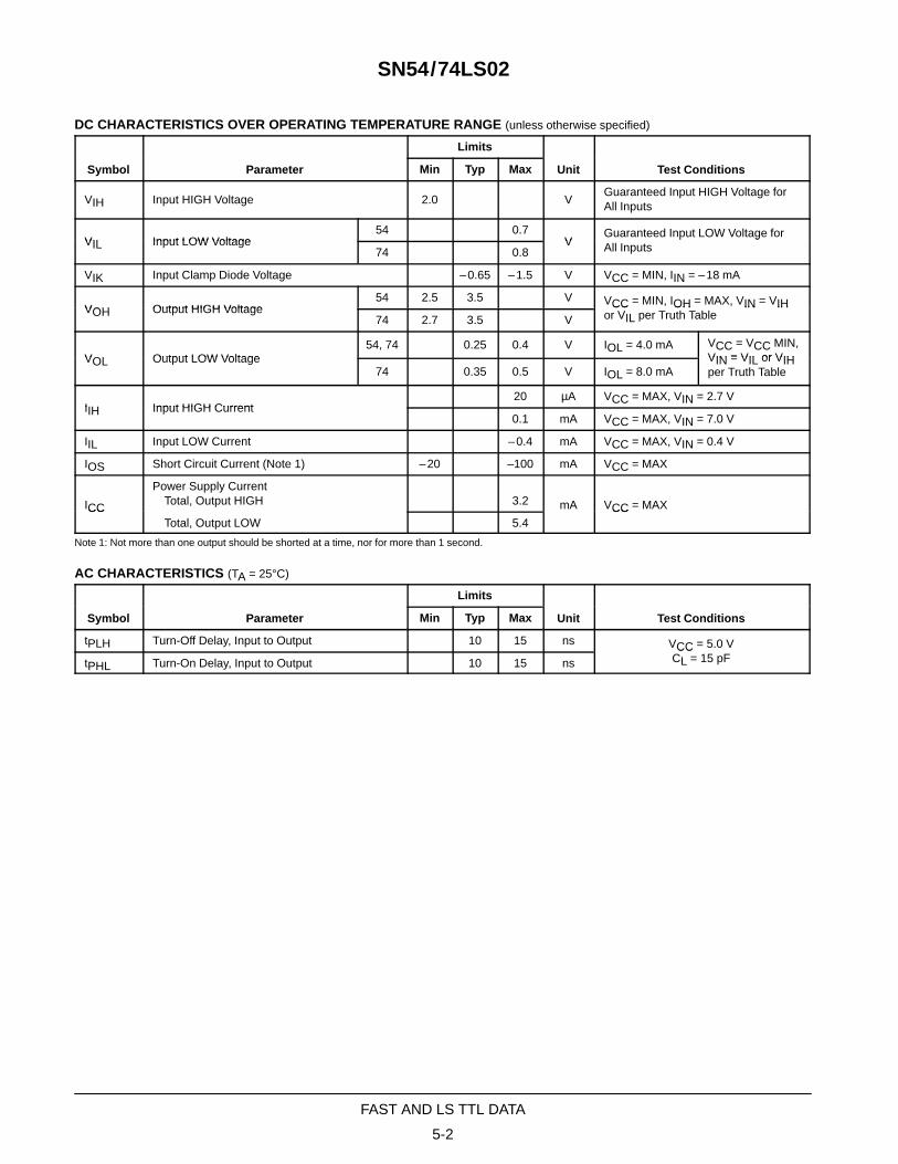

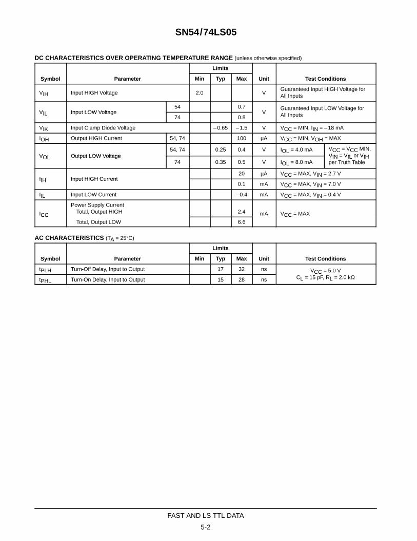


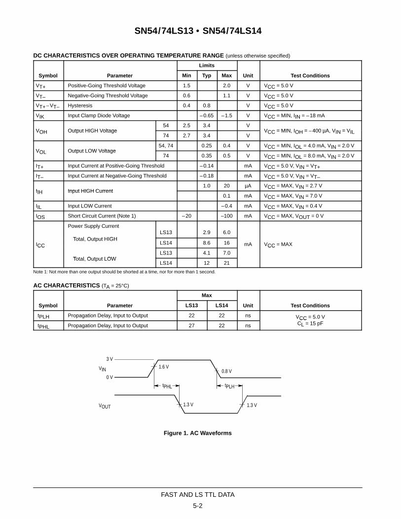


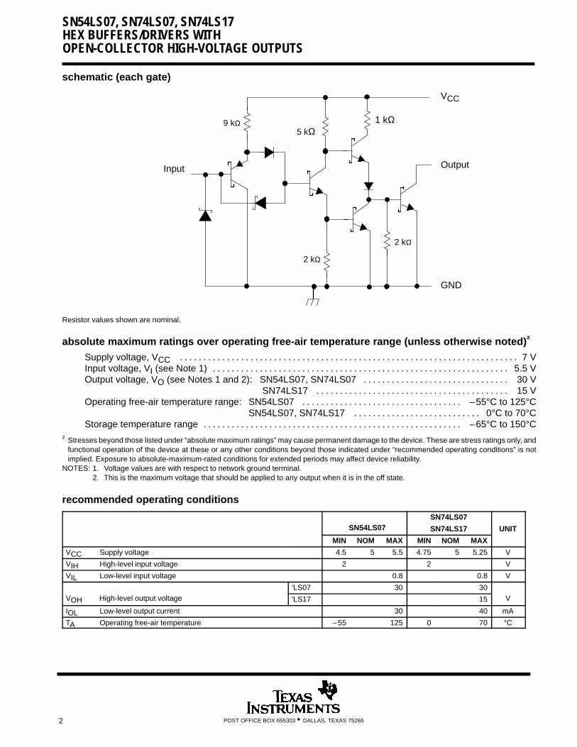

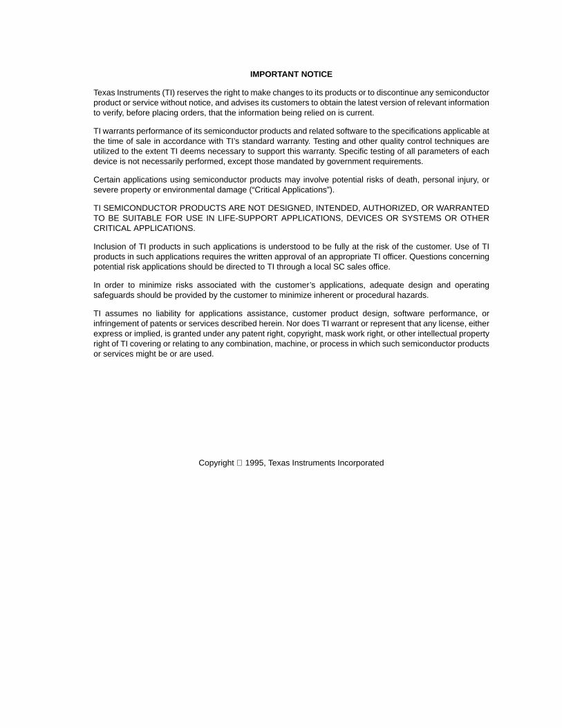


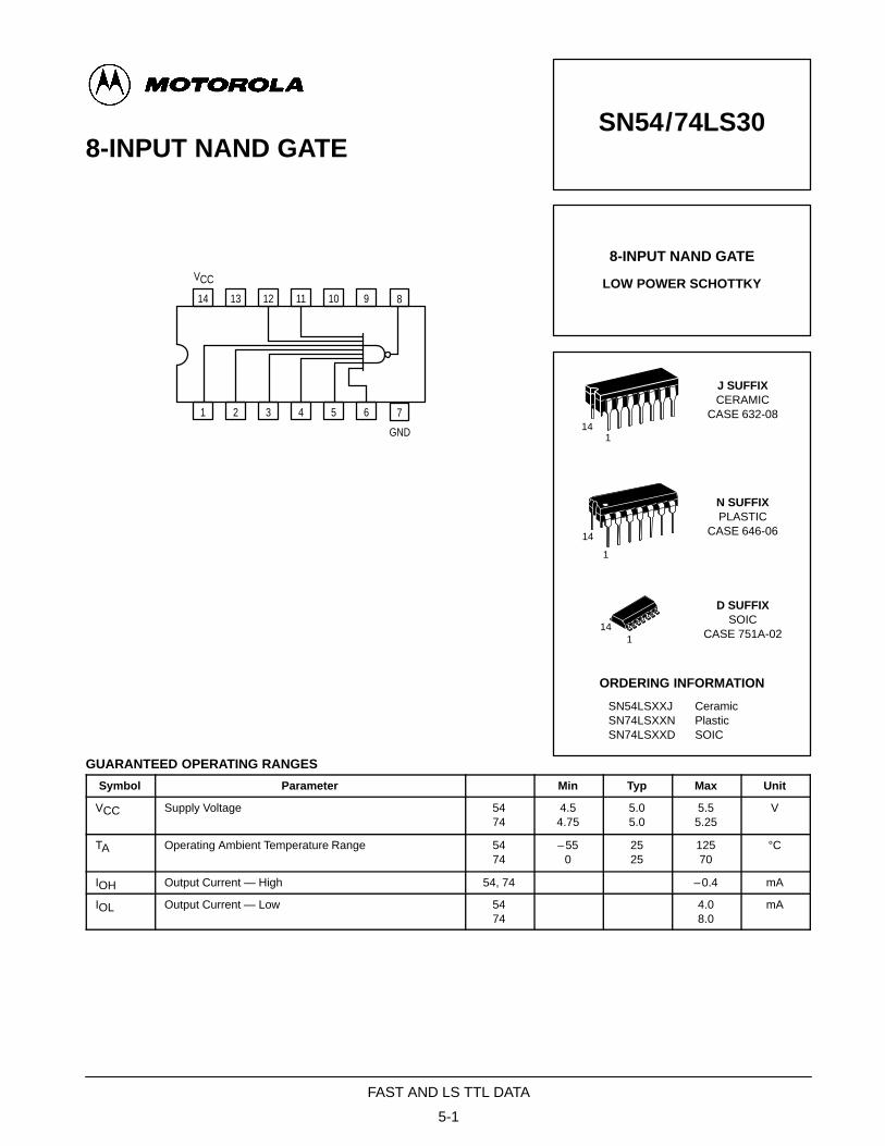


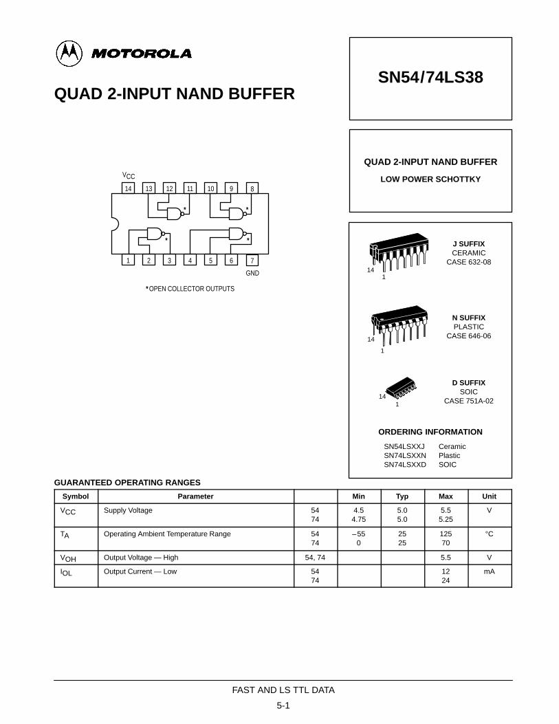


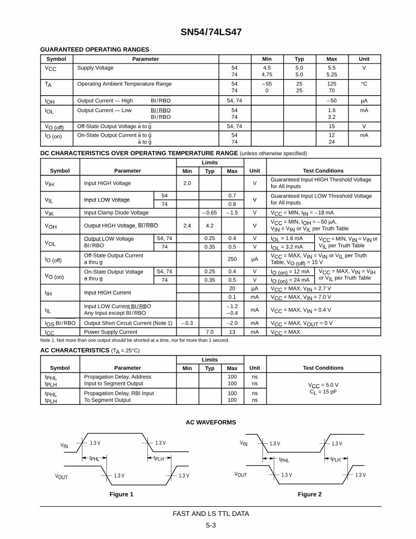


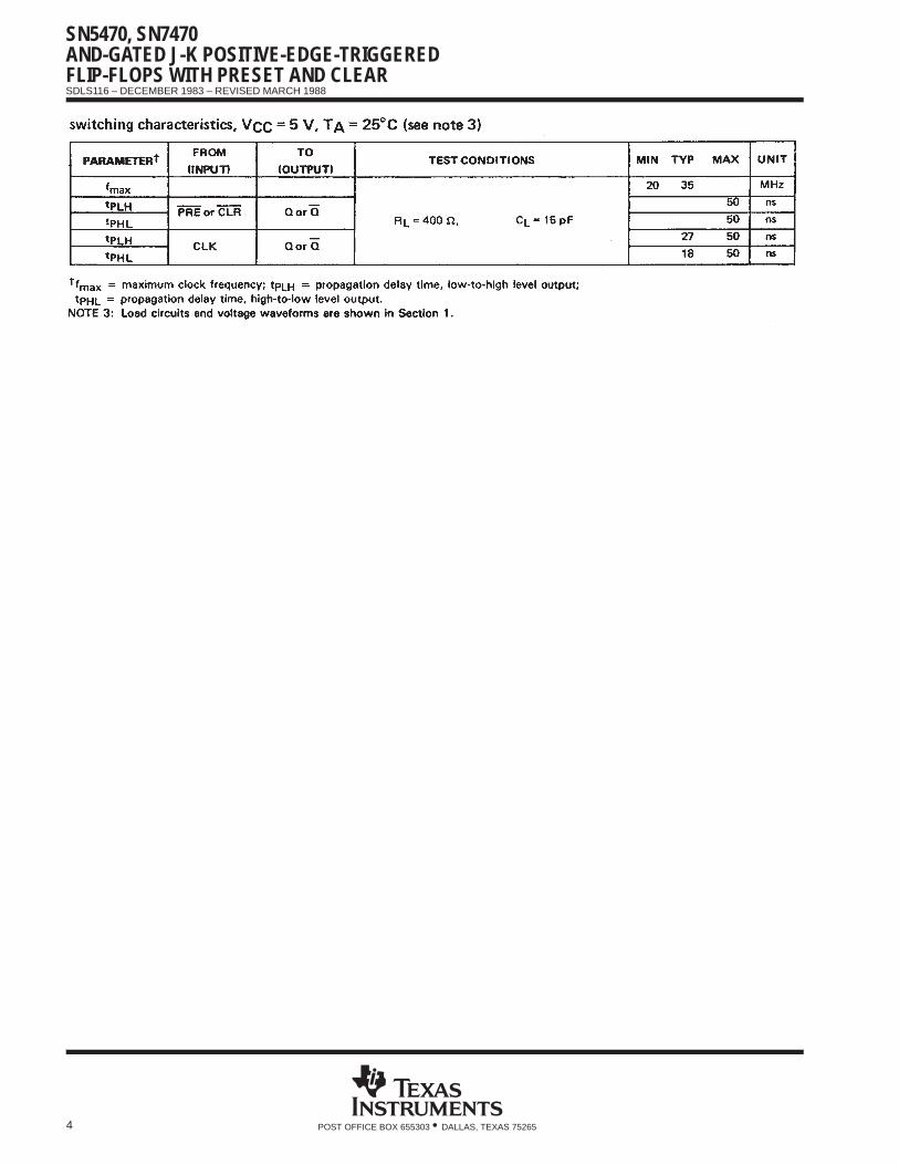


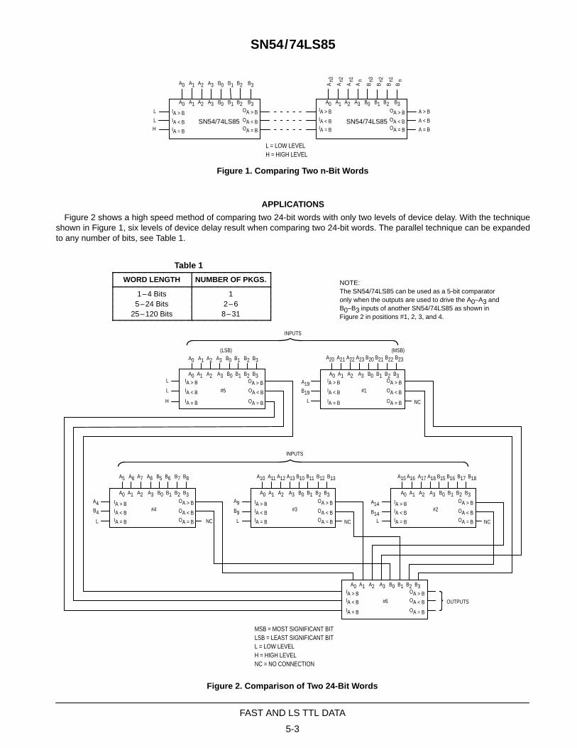

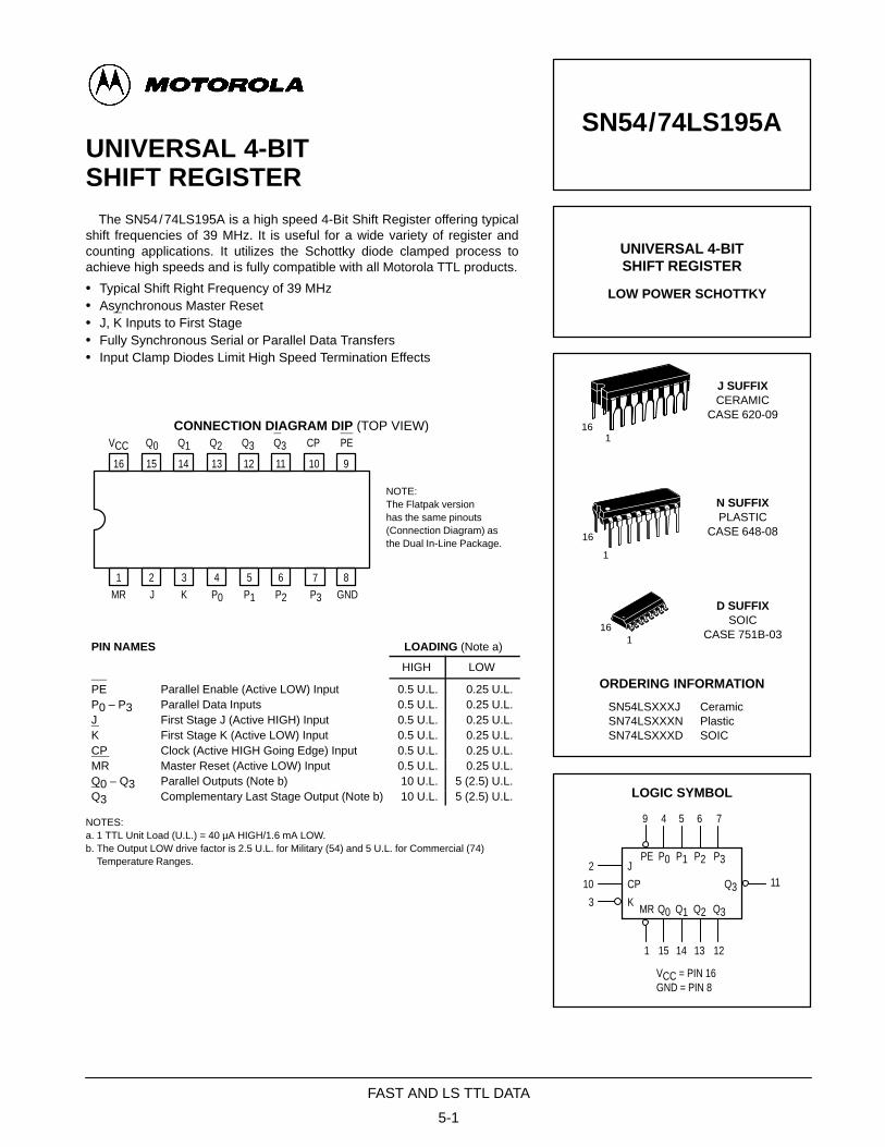


![74LVC86A Quad 2-input EXCLUSIVE-OR gate · Quad 2-input EXCLUSIVE-OR gate 10. Dynamic characteristics Table 7. Dynamic characteristics [1] Typical values are measured at Tamb =25](https://static.documents.pub/doc/80x56/5f3a7849701d7163b63d227f/74lvc86a-quad-2-input-exclusive-or-gate-quad-2-input-exclusive-or-gate-10-dynamic.jpg)