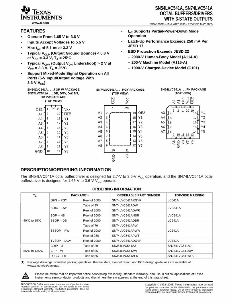
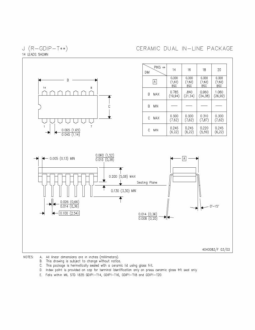
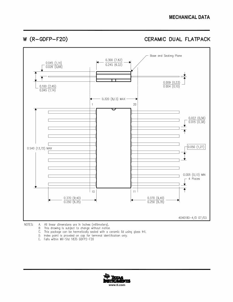
SN54LVC541A . . . J OR W PACKAGESN74LVC541A . . . DB, DGV, DW, NS,
OR PW PACKAGE(TOP VIEW)
3 2 1 20 19
9 10 11 12 13
4
5
6
7
8
18
17
16
15
14
Y1Y2Y3Y4Y5
A3A4A5A6A7
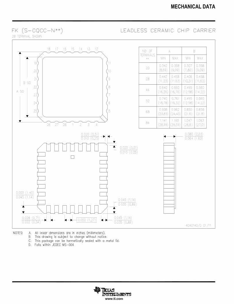
SN54LVC541A . . . FK PACKAGE(TOP VIEW)
A2
A1
OE
1Y
7Y
6O
E2
A8
GN
D Y8
VC
C
SN74LVC541A . . . RGY PACKAGE(TOP VIEW)
1 20
10 11
2
3
4
5
6
7
8
9
19
18
17
16
15
14
13
12
OE2Y1Y2Y3Y4Y5Y6Y7
A1A2A3A4A5A6A7A8
OE
1
Y8
V
GN
D
CC
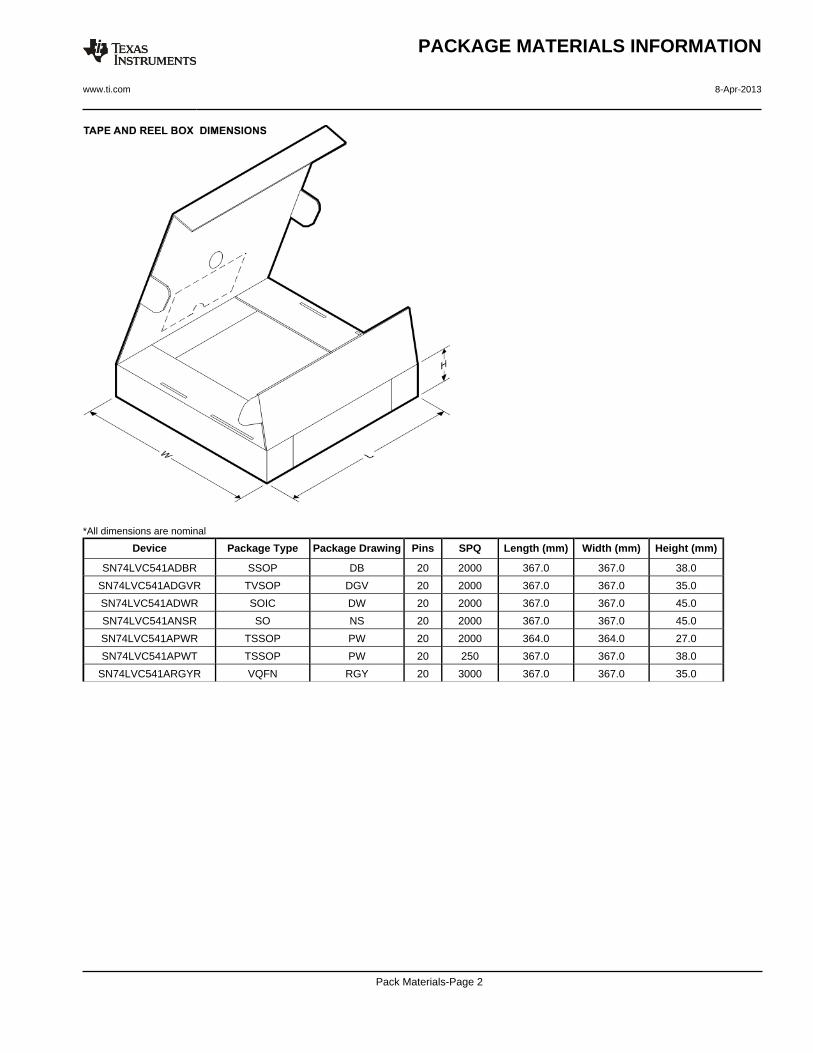
DESCRIPTION/ORDERING INFORMATION
SN54LVC541A, SN74LVC541AOCTAL BUFFERS/DRIVERS
WITH 3-STATE OUTPUTSSCAS298M–JANUARY 1993–REVISED MAY 2005
• Ioff Supports Partial-Power-Down ModeOperation• Operate From 1.65 V to 3.6 V
• Latch-Up Performance Exceeds 250 mA Per• Inputs Accept Voltages to 5.5 VJESD 17• Max tpd of 5.1 ns at 3.3 V
• ESD Protection Exceeds JESD 22• Typical VOLP (Output Ground Bounce) < 0.8 V– 2000-V Human-Body Model (A114-A)at VCC = 3.3 V, TA = 25°C– 200-V Machine Model (A115-A)• Typical VOHV (Output VOH Undershoot) > 2 V at
VCC = 3.3 V, TA = 25°C – 1000-V Charged-Device Model (C101)ABC• Support Mixed-Mode Signal Operation on All
Ports (5-V Input/Output Voltage With3.3-V VCC)
The SN54LVC541A octal buffer/driver is designed for 2.7-V to 3.6-V VCC operation, and the SN74LVC541A octalbuffer/driver is designed for 1.65-V to 3.6-V VCC operation.
ORDERING INFORMATION
TA PACKAGE (1) ORDERABLE PART NUMBER TOP-SIDE MARKING
QFN – RGY Reel of 1000 SN74LVC541ARGYR LC541A
Tube of 25 SN74LVC541ADWSOIC – DW LVC541A
Reel of 2000 SN74LVC541ADWR
SOP – NS Reel of 2000 SN74LVC541ANSR LVC541A
–40°C to 85°C SSOP – DB Reel of 2000 SN74LVC541ADBR LC541A
Tube of 70 SN74LVC541APW
TSSOP – PW Reel of 2000 SN74LVC541APWR LC541A
Reel of 250 SN74LVC541APWT
TVSOP – DGV Reel of 2000 SN74LVC541ADGVR LC541A
CDIP – J Tube of 20 SNJ54LVC541AJ SNJ54LVC541AJ
–55°C to 125°C CFP – W Tube of 85 SNJ54LVC541AW SNJ54LVC541AW
LCCC – FK Tube of 55 SNJ54LVC541AFK SNJ54LVC541AFK
(1) Package drawings, standard packing quantities, thermal data, symbolization, and PCB design guidelines are available atwww.ti.com/sc/package.
Please be aware that an important notice concerning availability, standard warranty, and use in critical applications of TexasInstruments semiconductor products and disclaimers thereto appears at the end of this data sheet.
SN54LVC541A, SN74LVC541AOCTAL BUFFERS/DRIVERSWITH 3-STATE OUTPUTSSCAS298M–JANUARY 1993–REVISED MAY 2005
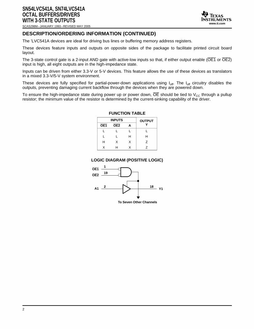
The 'LVC541A devices are ideal for driving bus lines or buffering memory address registers.
These devices feature inputs and outputs on opposite sides of the package to facilitate printed circuit boardlayout.
The 3-state control gate is a 2-input AND gate with active-low inputs so that, if either output enable (OE1 or OE2)input is high, all eight outputs are in the high-impedance state.
Inputs can be driven from either 3.3-V or 5-V devices. This feature allows the use of these devices as translatorsin a mixed 3.3-V/5-V system environment.
These devices are fully specified for partial-power-down applications using Ioff. The Ioff circuitry disables theoutputs, preventing damaging current backflow through the devices when they are powered down.
To ensure the high-impedance state during power up or power down, OE should be tied to VCC through a pullupresistor; the minimum value of the resistor is determined by the current-sinking capability of the driver.
FUNCTION TABLE
INPUTS OUTPUTYOE1 OE2 A
L L L L
L L H H
H X X Z
X H X Z
LOGIC DIAGRAM (POSITIVE LOGIC)
2
www.ti.com
Absolute Maximum Ratings (1)
SN54LVC541A, SN74LVC541AOCTAL BUFFERS/DRIVERS
WITH 3-STATE OUTPUTSSCAS298M–JANUARY 1993–REVISED MAY 2005
over operating free-air temperature range (unless otherwise noted)
MIN MAX UNIT
VCC Supply voltage range –0.5 6.5 V
VI Input voltage range (2) –0.5 6.5 V
VO Voltage range applied to any output in the high-impedance or power-off state (2) –0.5 6.5 V
VO Voltage range applied to any output in the high or low state (2) (3) –0.5 VCC + 0.5 V
(1) Stresses beyond those listed under "absolute maximum ratings" may cause permanent damage to the device. These are stress ratingsonly, and functional operation of the device at these or any other conditions beyond those indicated under "recommended operatingconditions" is not implied. Exposure to absolute-maximum-rated conditions for extended periods may affect device reliability.
(2) The input negative-voltage and output voltage ratings may be exceeded if the input and output current ratings are observed.(3) The value of VCC is provided in the recommended operating conditions table.(4) The package thermal impedance is calculated in accordance with JESD 51-7.(5) The package thermal impedance is calculated in accordance with JESD 51-5.
3
www.ti.com
Recommended Operating Conditions (1)
SN54LVC541A, SN74LVC541AOCTAL BUFFERS/DRIVERSWITH 3-STATE OUTPUTSSCAS298M–JANUARY 1993–REVISED MAY 2005
SN54LVC541A SN74LVC541AUNIT
MIN MAX MIN MAX
Operating 2 3.6 1.65 3.6VCC Supply voltage V
Data retention only 1.5 1.5
VCC = 1.65 V to 1.95 V 0.65 × VCC
VIH High-level input voltage VCC = 2.3 V to 2.7 V 1.7 V
VCC = 2.7 V to 3.6 V 2 2
VCC = 1.65 V to 1.95 V 0.35 × VCC
VIL Low-level input voltage VCC = 2.3 V to 2.7 V 0.7 V
VCC = 2.7 V to 3.6 V 0.8 0.8
VI Input voltage 0 5.5 0 5.5 V
High or low state 0 VCC 0 VCCVO Output voltage V
3-state 0 5.5 0 5.5
VCC = 1.65 V –4
VCC = 2.3 V –8IOH High-level output current mA
VCC = 2.7 V –12 –12
VCC = 3 V –24 –24
VCC = 1.65 V 4
VCC = 2.3 V 8IOL Low-level output current mA
VCC = 2.7 V 12 12
VCC = 3 V 24 24
TA Operating free-air temperature –55 125 –40 85 °C
(1) All unused inputs of the device must be held at VCC or GND to ensure proper device operation. Refer to the TI application report,Implications of Slow or Floating CMOS Inputs, literature number SCBA004.
4
www.ti.com
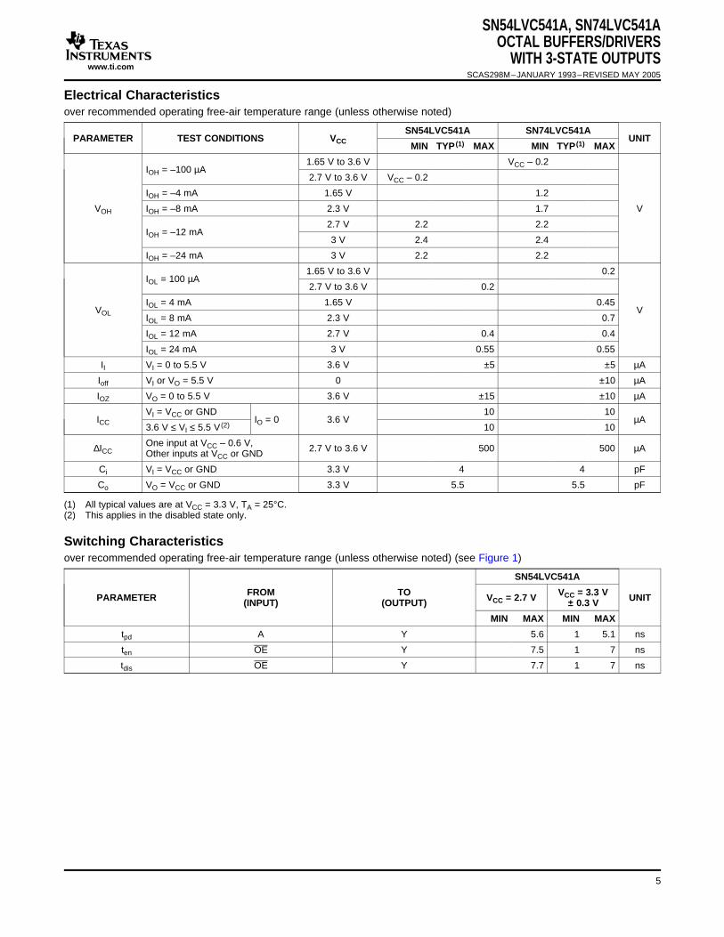
Electrical Characteristics
Switching Characteristics
SN54LVC541A, SN74LVC541AOCTAL BUFFERS/DRIVERS
WITH 3-STATE OUTPUTSSCAS298M–JANUARY 1993–REVISED MAY 2005
over recommended operating free-air temperature range (unless otherwise noted)
SN54LVC541A SN74LVC541APARAMETER TEST CONDITIONS VCC UNIT
MIN TYP (1) MAX MIN TYP (1) MAX
1.65 V to 3.6 V VCC – 0.2IOH = –100 µA
2.7 V to 3.6 V VCC – 0.2
IOH = –4 mA 1.65 V 1.2
VOH IOH = –8 mA 2.3 V 1.7 V
2.7 V 2.2 2.2IOH = –12 mA
3 V 2.4 2.4
IOH = –24 mA 3 V 2.2 2.2
1.65 V to 3.6 V 0.2IOL = 100 µA
2.7 V to 3.6 V 0.2
IOL = 4 mA 1.65 V 0.45VOL V
IOL = 8 mA 2.3 V 0.7
IOL = 12 mA 2.7 V 0.4 0.4
IOL = 24 mA 3 V 0.55 0.55
II VI = 0 to 5.5 V 3.6 V ±5 ±5 µA
Ioff VI or VO = 5.5 V 0 ±10 µA
IOZ VO = 0 to 5.5 V 3.6 V ±15 ±10 µA
VI = VCC or GND 10 10ICC IO = 0 3.6 V µA
3.6 V ≤ VI ≤ 5.5 V (2) 10 10
One input at VCC – 0.6 V,∆ICC 2.7 V to 3.6 V 500 500 µAOther inputs at VCC or GND
Ci VI = VCC or GND 3.3 V 4 4 pF
Co VO = VCC or GND 3.3 V 5.5 5.5 pF
(1) All typical values are at VCC = 3.3 V, TA = 25°C.(2) This applies in the disabled state only.
over recommended operating free-air temperature range (unless otherwise noted) (see Figure 1)
SN54LVC541A
FROM TO VCC = 3.3 VPARAMETER VCC = 2.7 V UNIT(INPUT) (OUTPUT) ± 0.3 V
MIN MAX MIN MAX
tpd A Y 5.6 1 5.1 ns
ten OE Y 7.5 1 7 ns
tdis OE Y 7.7 1 7 ns
5
www.ti.com
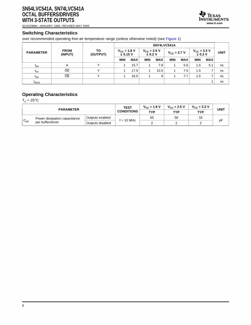
Switching Characteristics
Operating Characteristics
SN54LVC541A, SN74LVC541AOCTAL BUFFERS/DRIVERSWITH 3-STATE OUTPUTSSCAS298M–JANUARY 1993–REVISED MAY 2005
over recommended operating free-air temperature range (unless otherwise noted) (see Figure 1)
SN74LVC541A
FROM TO VCC = 1.8 V VCC = 2.5 V VCC = 3.3 VPARAMETER VCC = 2.7 V UNIT(INPUT) (OUTPUT) ± 0.15 V ± 0.2 V ± 0.3 V
MIN MAX MIN MAX MIN MAX MIN MAX
tpd A Y 1 15.7 1 7.8 1 5.6 1.5 5.1 ns
ten OE Y 1 17.5 1 10.5 1 7.5 1.5 7 ns
tdis OE Y 1 16.5 1 9 1 7.7 1.5 7 ns
tsk(o) 1 ns
TA = 25°C
VCC = 1.8 V VCC = 2.5 V VCC = 3.3 VTESTPARAMETER UNITCONDITIONS TYP TYP TYP
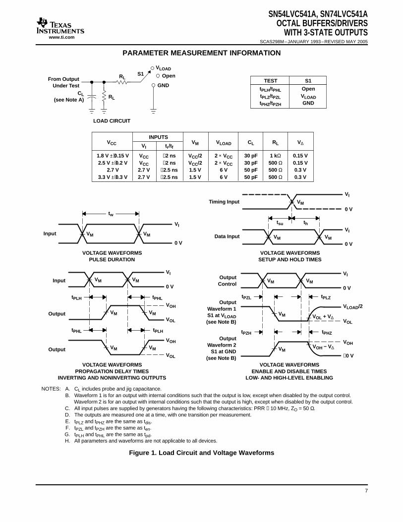
NOTES: A. CL includes probe and jig capacitance.B. Waveform 1 is for an output with internal conditions such that the output is low, except when disabled by the output control.
Waveform 2 is for an output with internal conditions such that the output is high, except when disabled by the output control.C. All input pulses are supplied by generators having the following characteristics: PRR ≤ 10 MHz, ZO = 50 Ω.D. The outputs are measured one at a time, with one transition per measurement.E. tPLZ and tPHZ are the same as tdis.F. tPZL and tPZH are the same as ten.G. tPLH and tPHL are the same as tpd.H. All parameters and waveforms are not applicable to all devices.
OutputControl
VM VM
VM VM
VM VM
VM
VM VM
VM
VM
VM
VI
VM
VM
1.8 V ± 0.15 V2.5 V ± 0.2 V
2.7 V3.3 V ± 0.3 V
1 kΩ500 Ω500 Ω500 Ω
VCC RL
2 × VCC2 × VCC
6 V6 V
VLOAD CL
30 pF30 pF50 pF50 pF
0.15 V0.15 V0.3 V0.3 V
V∆
VCCVCC2.7 V2.7 V
VI
VCC/2VCC/21.5 V1.5 V
VMtr/tf
≤2 ns≤2 ns
≤2.5 ns≤2.5 ns
INPUTS
SN54LVC541A, SN74LVC541AOCTAL BUFFERS/DRIVERS
WITH 3-STATE OUTPUTSSCAS298M–JANUARY 1993–REVISED MAY 2005
Figure 1. Load Circuit and Voltage Waveforms
7
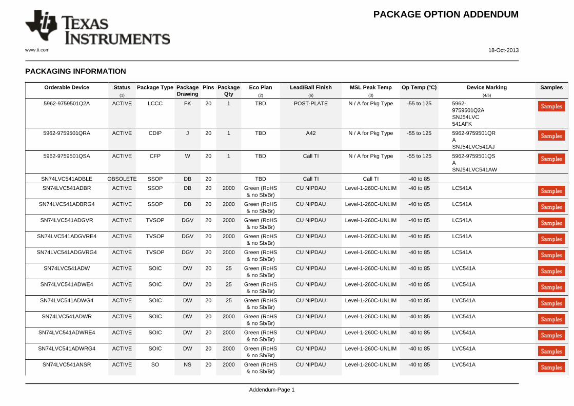
PACKAGE OPTION ADDENDUM
www.ti.com 18-Oct-2013
Addendum-Page 1
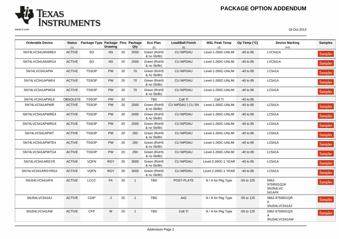
PACKAGING INFORMATION
Orderable Device Status(1)
Package Type PackageDrawing
Pins PackageQty
Eco Plan(2)
Lead/Ball Finish(6)
MSL Peak Temp(3)
Op Temp (°C) Device Marking(4/5)
Samples
5962-9759501Q2A ACTIVE LCCC FK 20 1 TBD POST-PLATE N / A for Pkg Type -55 to 125 5962-9759501Q2ASNJ54LVC541AFK
5962-9759501QRA ACTIVE CDIP J 20 1 TBD A42 N / A for Pkg Type -55 to 125 5962-9759501QRASNJ54LVC541AJ
5962-9759501QSA ACTIVE CFP W 20 1 TBD Call TI N / A for Pkg Type -55 to 125 5962-9759501QSASNJ54LVC541AW
SN74LVC541ADBLE OBSOLETE SSOP DB 20 TBD Call TI Call TI -40 to 85
SN74LVC541ADBR ACTIVE SSOP DB 20 2000 Green (RoHS& no Sb/Br)
CU NIPDAU Level-1-260C-UNLIM -40 to 85 LC541A
SN74LVC541ADBRG4 ACTIVE SSOP DB 20 2000 Green (RoHS& no Sb/Br)
CU NIPDAU Level-1-260C-UNLIM -40 to 85 LC541A
SN74LVC541ADGVR ACTIVE TVSOP DGV 20 2000 Green (RoHS& no Sb/Br)
CU NIPDAU Level-1-260C-UNLIM -40 to 85 LC541A
SN74LVC541ADGVRE4 ACTIVE TVSOP DGV 20 2000 Green (RoHS& no Sb/Br)
CU NIPDAU Level-1-260C-UNLIM -40 to 85 LC541A
SN74LVC541ADGVRG4 ACTIVE TVSOP DGV 20 2000 Green (RoHS& no Sb/Br)
CU NIPDAU Level-1-260C-UNLIM -40 to 85 LC541A
SN74LVC541ADW ACTIVE SOIC DW 20 25 Green (RoHS& no Sb/Br)
CU NIPDAU Level-1-260C-UNLIM -40 to 85 LVC541A
SN74LVC541ADWE4 ACTIVE SOIC DW 20 25 Green (RoHS& no Sb/Br)
CU NIPDAU Level-1-260C-UNLIM -40 to 85 LVC541A
SN74LVC541ADWG4 ACTIVE SOIC DW 20 25 Green (RoHS& no Sb/Br)
CU NIPDAU Level-1-260C-UNLIM -40 to 85 LVC541A
SN74LVC541ADWR ACTIVE SOIC DW 20 2000 Green (RoHS& no Sb/Br)
CU NIPDAU Level-1-260C-UNLIM -40 to 85 LVC541A
SN74LVC541ADWRE4 ACTIVE SOIC DW 20 2000 Green (RoHS& no Sb/Br)
CU NIPDAU Level-1-260C-UNLIM -40 to 85 LVC541A
SN74LVC541ADWRG4 ACTIVE SOIC DW 20 2000 Green (RoHS& no Sb/Br)
CU NIPDAU Level-1-260C-UNLIM -40 to 85 LVC541A
SN74LVC541ANSR ACTIVE SO NS 20 2000 Green (RoHS& no Sb/Br)
(1) The marketing status values are defined as follows:ACTIVE: Product device recommended for new designs.LIFEBUY: TI has announced that the device will be discontinued, and a lifetime-buy period is in effect.NRND: Not recommended for new designs. Device is in production to support existing customers, but TI does not recommend using this part in a new design.PREVIEW: Device has been announced but is not in production. Samples may or may not be available.OBSOLETE: TI has discontinued the production of the device.
(2) Eco Plan - The planned eco-friendly classification: Pb-Free (RoHS), Pb-Free (RoHS Exempt), or Green (RoHS & no Sb/Br) - please check http://www.ti.com/productcontent for the latest availabilityinformation and additional product content details.TBD: The Pb-Free/Green conversion plan has not been defined.Pb-Free (RoHS): TI's terms "Lead-Free" or "Pb-Free" mean semiconductor products that are compatible with the current RoHS requirements for all 6 substances, including the requirement thatlead not exceed 0.1% by weight in homogeneous materials. Where designed to be soldered at high temperatures, TI Pb-Free products are suitable for use in specified lead-free processes.Pb-Free (RoHS Exempt): This component has a RoHS exemption for either 1) lead-based flip-chip solder bumps used between the die and package, or 2) lead-based die adhesive used betweenthe die and leadframe. The component is otherwise considered Pb-Free (RoHS compatible) as defined above.Green (RoHS & no Sb/Br): TI defines "Green" to mean Pb-Free (RoHS compatible), and free of Bromine (Br) and Antimony (Sb) based flame retardants (Br or Sb do not exceed 0.1% by weightin homogeneous material)
(3) MSL, Peak Temp. - The Moisture Sensitivity Level rating according to the JEDEC industry standard classifications, and peak solder temperature.
(4) There may be additional marking, which relates to the logo, the lot trace code information, or the environmental category on the device.
(5) Multiple Device Markings will be inside parentheses. Only one Device Marking contained in parentheses and separated by a "~" will appear on a device. If a line is indented then it is a continuationof the previous line and the two combined represent the entire Device Marking for that device.
(6) Lead/Ball Finish - Orderable Devices may have multiple material finish options. Finish options are separated by a vertical ruled line. Lead/Ball Finish values may wrap to two lines if the finishvalue exceeds the maximum column width.
Important Information and Disclaimer:The information provided on this page represents TI's knowledge and belief as of the date that it is provided. TI bases its knowledge and belief on informationprovided by third parties, and makes no representation or warranty as to the accuracy of such information. Efforts are underway to better integrate information from third parties. TI has taken andcontinues to take reasonable steps to provide representative and accurate information but may not have conducted destructive testing or chemical analysis on incoming materials and chemicals.TI and TI suppliers consider certain information to be proprietary, and thus CAS numbers and other limited information may not be available for release.
In no event shall TI's liability arising out of such information exceed the total purchase price of the TI part(s) at issue in this document sold by TI to Customer on an annual basis.
OTHER QUALIFIED VERSIONS OF SN54LVC541A, SN74LVC541A :
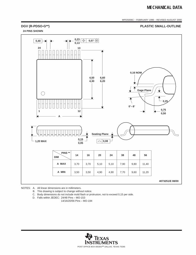
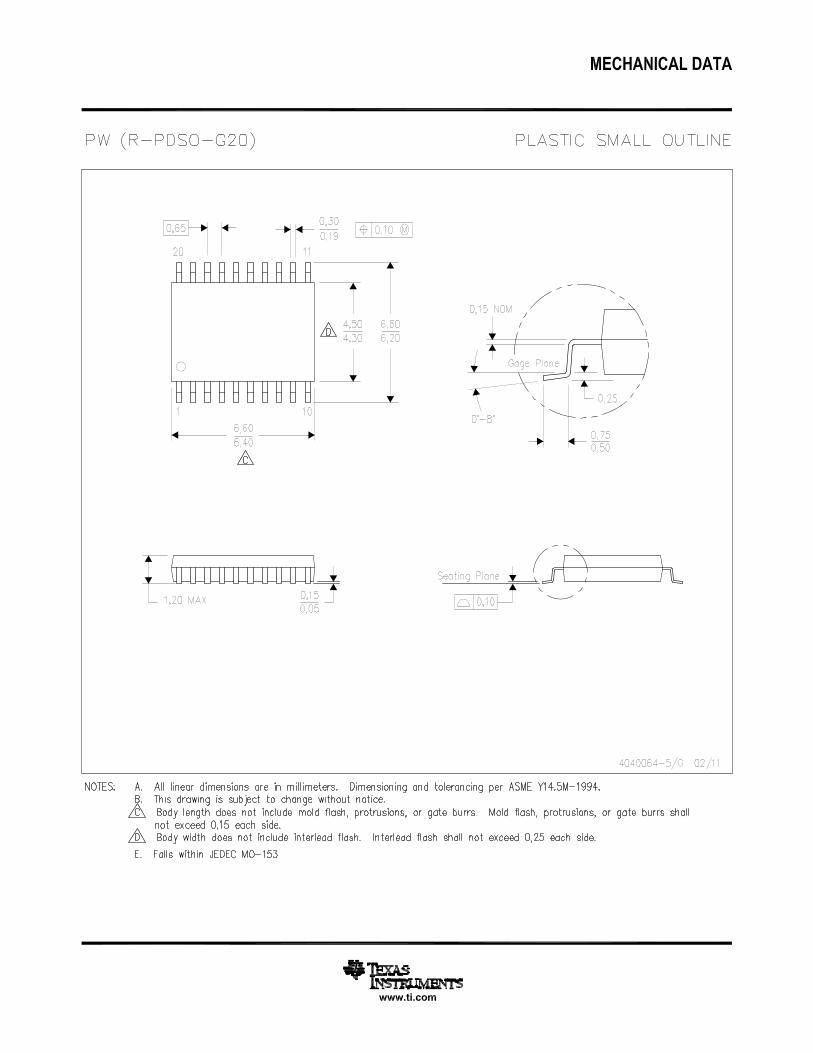
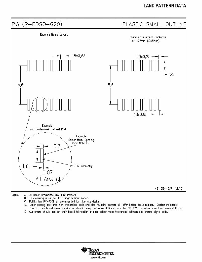
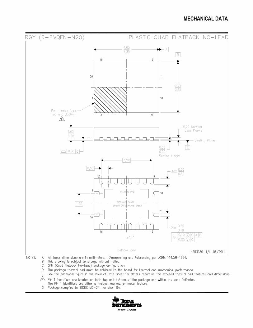
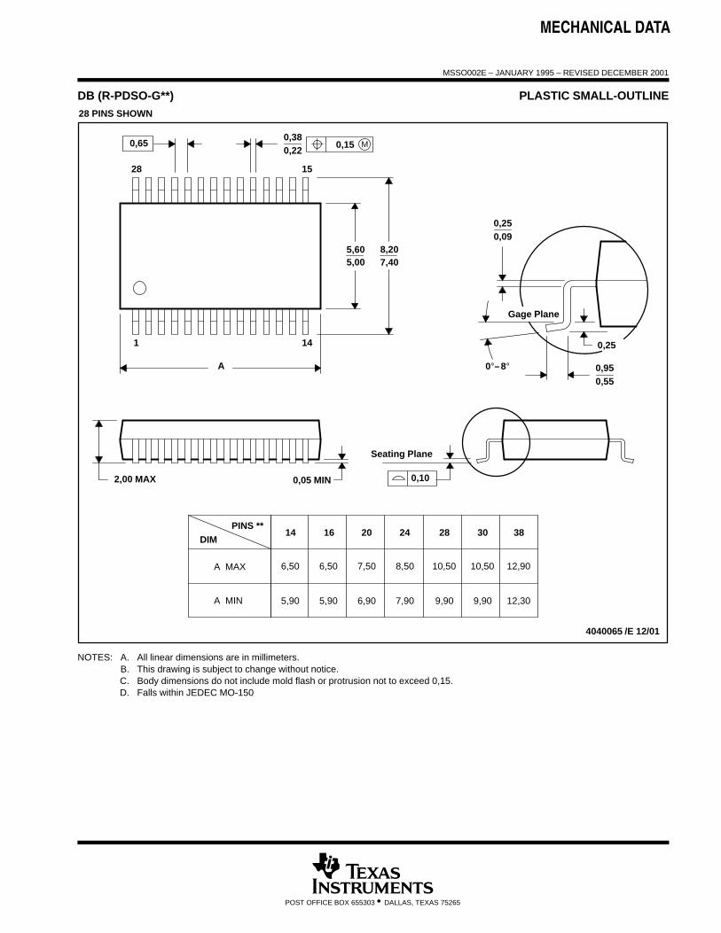
NOTES: A. All linear dimensions are in millimeters.B. This drawing is subject to change without notice.C. Body dimensions do not include mold flash or protrusion, not to exceed 0,15 per side.D. Falls within JEDEC: 24/48 Pins – MO-153
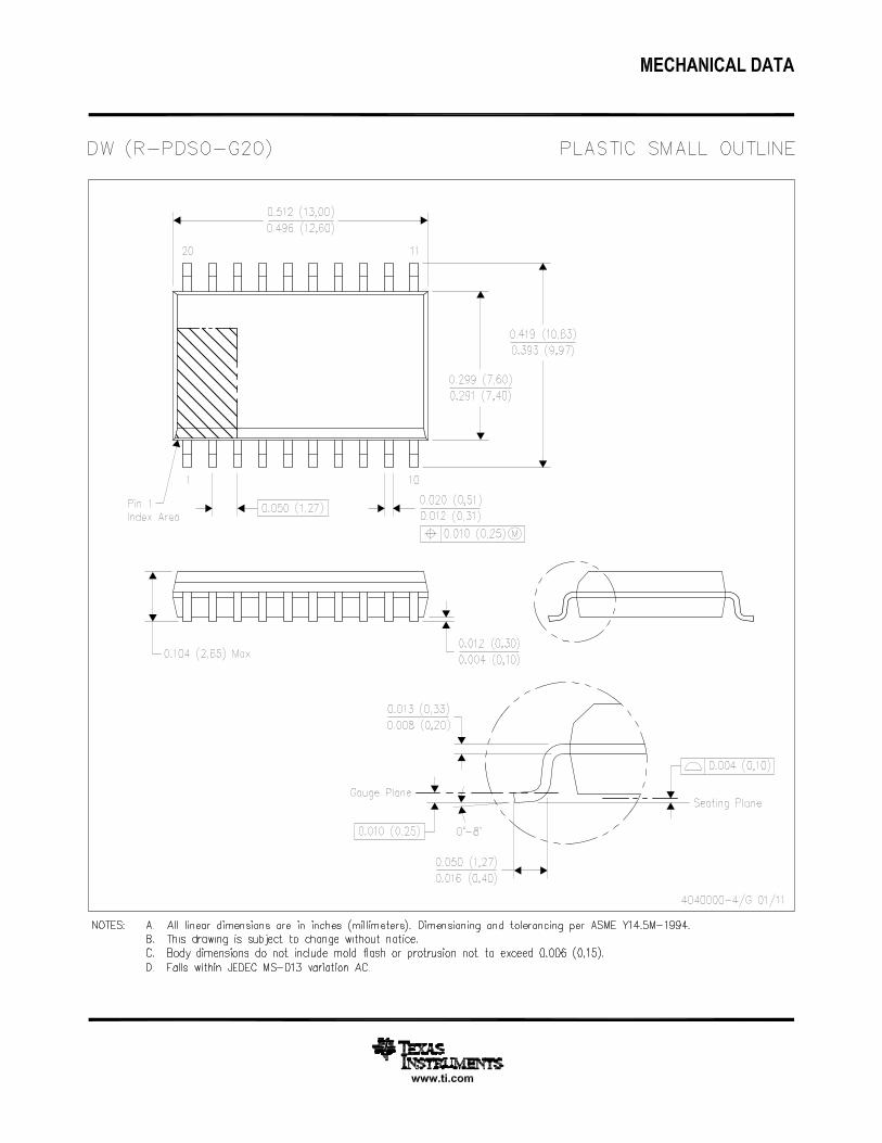
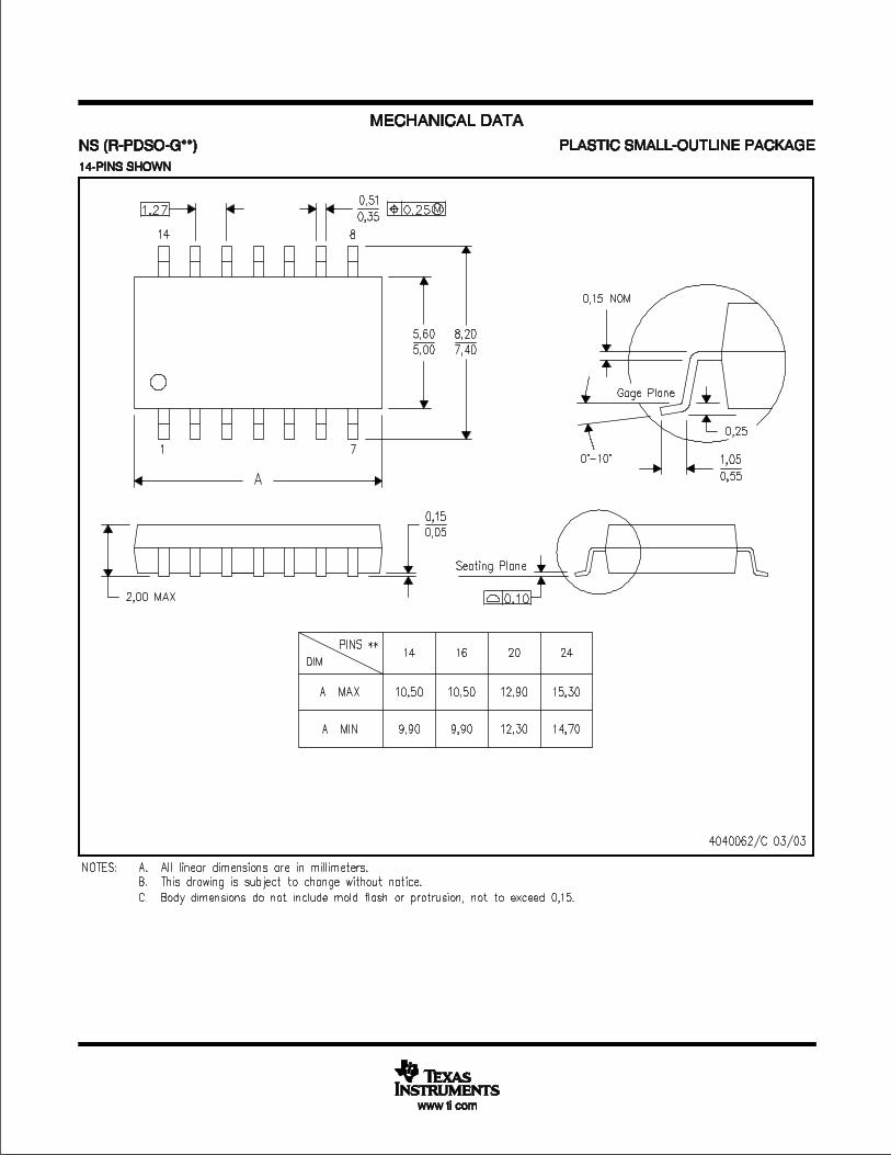
NOTES: A. All linear dimensions are in millimeters.B. This drawing is subject to change without notice.C. Body dimensions do not include mold flash or protrusion not to exceed 0,15.D. Falls within JEDEC MO-150
IMPORTANT NOTICE
Texas Instruments Incorporated and its subsidiaries (TI) reserve the right to make corrections, enhancements, improvements and otherchanges to its semiconductor products and services per JESD46, latest issue, and to discontinue any product or service per JESD48, latestissue. Buyers should obtain the latest relevant information before placing orders and should verify that such information is current andcomplete. All semiconductor products (also referred to herein as “components”) are sold subject to TI’s terms and conditions of salesupplied at the time of order acknowledgment.
TI warrants performance of its components to the specifications applicable at the time of sale, in accordance with the warranty in TI’s termsand conditions of sale of semiconductor products. Testing and other quality control techniques are used to the extent TI deems necessaryto support this warranty. Except where mandated by applicable law, testing of all parameters of each component is not necessarilyperformed.
TI assumes no liability for applications assistance or the design of Buyers’ products. Buyers are responsible for their products andapplications using TI components. To minimize the risks associated with Buyers’ products and applications, Buyers should provideadequate design and operating safeguards.
TI does not warrant or represent that any license, either express or implied, is granted under any patent right, copyright, mask work right, orother intellectual property right relating to any combination, machine, or process in which TI components or services are used. Informationpublished by TI regarding third-party products or services does not constitute a license to use such products or services or a warranty orendorsement thereof. Use of such information may require a license from a third party under the patents or other intellectual property of thethird party, or a license from TI under the patents or other intellectual property of TI.
Reproduction of significant portions of TI information in TI data books or data sheets is permissible only if reproduction is without alterationand is accompanied by all associated warranties, conditions, limitations, and notices. TI is not responsible or liable for such altereddocumentation. Information of third parties may be subject to additional restrictions.
Resale of TI components or services with statements different from or beyond the parameters stated by TI for that component or servicevoids all express and any implied warranties for the associated TI component or service and is an unfair and deceptive business practice.TI is not responsible or liable for any such statements.
Buyer acknowledges and agrees that it is solely responsible for compliance with all legal, regulatory and safety-related requirementsconcerning its products, and any use of TI components in its applications, notwithstanding any applications-related information or supportthat may be provided by TI. Buyer represents and agrees that it has all the necessary expertise to create and implement safeguards whichanticipate dangerous consequences of failures, monitor failures and their consequences, lessen the likelihood of failures that might causeharm and take appropriate remedial actions. Buyer will fully indemnify TI and its representatives against any damages arising out of the useof any TI components in safety-critical applications.
In some cases, TI components may be promoted specifically to facilitate safety-related applications. With such components, TI’s goal is tohelp enable customers to design and create their own end-product solutions that meet applicable functional safety standards andrequirements. Nonetheless, such components are subject to these terms.
No TI components are authorized for use in FDA Class III (or similar life-critical medical equipment) unless authorized officers of the partieshave executed a special agreement specifically governing such use.
Only those TI components which TI has specifically designated as military grade or “enhanced plastic” are designed and intended for use inmilitary/aerospace applications or environments. Buyer acknowledges and agrees that any military or aerospace use of TI componentswhich have not been so designated is solely at the Buyer's risk, and that Buyer is solely responsible for compliance with all legal andregulatory requirements in connection with such use.
TI has specifically designated certain components as meeting ISO/TS16949 requirements, mainly for automotive use. In any case of use ofnon-designated products, TI will not be responsible for any failure to meet ISO/TS16949.
Products Applications
Audio www.ti.com/audio Automotive and Transportation www.ti.com/automotive
Amplifiers amplifier.ti.com Communications and Telecom www.ti.com/communications
Data Converters dataconverter.ti.com Computers and Peripherals www.ti.com/computers