VCC CANH 7 6 CANL RXD 1 TXD S 8 DOMINANT TIME OUT OVER TEMPERATURE LOGIC OUTPUT MODE SELECT 4 NC / VRXD / FAULT (See Note A) VCC 5 3 GND 2 UNDER VOLTAGE DOMINANT TIME OUT (See Note C) VCC VCC or VRXD (See Note B) FAULT LOGIC MUX (See Note A) BIAS UNIT Product Folder Sample & Buy Technical Documents Tools & Software Support & Community SN65HVD265, SN65HVD266, SN65HVD267 SLLSEI3A – SEPTEMBER 2013 – REVISED NOVEMBER 2015 SN65HVD26x Turbo CAN Transceivers for CAN FD (Flexible Data Rate) and Redundancy 1 Features 3 Description This CAN transceiver meets the ISO1189-2 High 1• Meets the Requirements of ISO11898-2 Speed CAN (Controller Area Network) physical layer • Turbo CAN: standard. It is designed for data rates in excess of 2 – Specified for 2-Mbps CAN FD (CAN with Mpbs (megabits per second) for CAN FD (CAN with Flexible Data Rate) flexible data rate), greater than 1 Mbps for CAN in short networks, and enhanced timing margin and – Short and Symmetrical Propagation Delay higher data rates in long and highly-loaded networks. Times and Fast Loop Times for Enhanced The device provides many protection features to Timing Margin enhance device and CAN-network robustness. The – Higher Data Rates in CAN Networks SN65HVD267 adds additional features, allowing easy design of redundant and multi-topology networks with • I/O Voltage Range Supports 3.3-V and 5-V MCUs fault indication for higher levels of safety in the CAN • Ideal Passive Behavior When Unpowered system. – Bus and Logic Terminals are High Impedance (no load) Device Information (1) – Power-Up/Down With Glitch Free Operation PART NUMBER PACKAGE BODY SIZE On Bus SN65HVD26xD SOIC (8) 4.90 mm × 3.91 mm • Protection Features (1) For all available packages, see the orderable addendum at the end of the data sheet. – HBM ESD Protection Exceeds ±12 kV – Bus Fault Protection –27 V to 40 V Functional Block Diagram – Undervoltage Protection on Supply Terminals – Driver Dominant Time Out (TXD DTO) – SN65HVD267: Receiver Dominant Time Out (RXD DTO) – SN65HVD267: FAULT Output Terminal – Thermal Shutdown Protection • Characterized for –40°C to 125°C Operation 2 Applications • 2-Mbps Operation in CAN with Flexible Data Rate Networks • 1-Mbps Operation in Highly Loaded CAN Networks Down to 10-kbps Networks Using TXD DTO • Industrial Automation, Control, Sensors and Drive Terminal 5 function is device dependent; Systems NC on SN65HVD265, V RXD for RXD output • Building, Security and Climate Control Automation level-shifting device on SN65HVD266, and FAULT Output on SN65HVD267 • Telecom Base Station Status and Control RXD logic output is driven to 5V V CC on • SN65HVD267: Functional Safety With Redundant 5V-only supply devices (SN65HVD265, and Multi-topology CAN networks SN65HVD267) and driven to V RXD on output level-shifting device (SN65HVD266). • CAN Bus Standards Such as CANopen, RXD (Receiver) Dominant State Time Out DeviceNet, NMEA2000, ARNIC825, ISO11783, is a device dependent option available only CANaerospace on SN65HVD267. 1 An IMPORTANT NOTICE at the end of this data sheet addresses availability, warranty, changes, use in safety-critical applications, intellectual property matters and other important disclaimers. PRODUCTION DATA.
Transcript
VCC
CANH7
6 CANL
RXD
1TXD
S8
DOMINANTTIME OUT
OVER TEMPERATURE
LOGIC OUTPUT
MODE SELECT
4
NC / VRXD / FAULT (See Note A) VCC
5 3
GND
2
UNDERVOLTAGE
DOMINANTTIME OUT
(See Note C)
VCC
VCC or VRXD (See Note B)
FAULT LOGIC MUX (See Note A)
BIA
S U
NIT
Product
Folder
Sample &Buy
Technical
Documents
Tools &
Software
Support &Community
SN65HVD265, SN65HVD266, SN65HVD267SLLSEI3A –SEPTEMBER 2013–REVISED NOVEMBER 2015
SN65HVD26x Turbo CAN Transceivers for CAN FD (Flexible Data Rate) and Redundancy1 Features 3 Description
This CAN transceiver meets the ISO1189-2 High1• Meets the Requirements of ISO11898-2
Speed CAN (Controller Area Network) physical layer• Turbo CAN: standard. It is designed for data rates in excess of 2– Specified for 2-Mbps CAN FD (CAN with Mpbs (megabits per second) for CAN FD (CAN with
Flexible Data Rate) flexible data rate), greater than 1 Mbps for CAN inshort networks, and enhanced timing margin and– Short and Symmetrical Propagation Delayhigher data rates in long and highly-loaded networks.Times and Fast Loop Times for EnhancedThe device provides many protection features toTiming Margin enhance device and CAN-network robustness. The
– Higher Data Rates in CAN Networks SN65HVD267 adds additional features, allowing easydesign of redundant and multi-topology networks with• I/O Voltage Range Supports 3.3-V and 5-V MCUsfault indication for higher levels of safety in the CAN• Ideal Passive Behavior When Unpoweredsystem.
– Bus and Logic Terminals are High Impedance(no load) Device Information (1)
– Power-Up/Down With Glitch Free Operation PART NUMBER PACKAGE BODY SIZEOn Bus SN65HVD26xD SOIC (8) 4.90 mm × 3.91 mm
• Protection Features (1) For all available packages, see the orderable addendum atthe end of the data sheet.– HBM ESD Protection Exceeds ±12 kV
– Bus Fault Protection –27 V to 40 V Functional Block Diagram– Undervoltage Protection on Supply Terminals– Driver Dominant Time Out (TXD DTO)– SN65HVD267: Receiver Dominant Time Out
2 Applications• 2-Mbps Operation in CAN with Flexible Data Rate
Networks• 1-Mbps Operation in Highly Loaded CAN
Networks Down to 10-kbps Networks Using TXDDTO
• Industrial Automation, Control, Sensors and DriveTerminal 5 function is device dependent;Systems NC on SN65HVD265, VRXD for RXD output
• Building, Security and Climate Control Automation level-shifting device on SN65HVD266, andFAULT Output on SN65HVD267• Telecom Base Station Status and ControlRXD logic output is driven to 5V VCC on• SN65HVD267: Functional Safety With Redundant 5V-only supply devices (SN65HVD265,
and Multi-topology CAN networks SN65HVD267) and driven to VRXD onoutput level-shifting device (SN65HVD266).• CAN Bus Standards Such as CANopen,RXD (Receiver) Dominant State Time OutDeviceNet, NMEA2000, ARNIC825, ISO11783,is a device dependent option available onlyCANaerospaceon SN65HVD267.
1
An IMPORTANT NOTICE at the end of this data sheet addresses availability, warranty, changes, use in safety-critical applications,intellectual property matters and other important disclaimers. PRODUCTION DATA.
13 Device and Documentation Support ................. 267.5 Recommended Operating Conditions....................... 513.1 Related Links ........................................................ 267.6 Thermal Information .................................................. 513.2 Community Resources.......................................... 267.7 Electrical Characteristics........................................... 513.3 Trademarks ........................................................... 267.8 Switching Characteristics .......................................... 813.4 Electrostatic Discharge Caution............................ 267.9 Typical Characteristics .............................................. 913.5 Glossary ................................................................ 268 Parameter Measurement Information .................. 9
14 Mechanical, Packaging, and Orderable9 Detailed Description ............................................ 13 Information ........................................................... 26
4 Revision HistoryNOTE: Page numbers for previous revisions may differ from page numbers in the current version.
Changes from Original (September 2013) to Revision A Page
• Added Pin Configuration and Functions section, ESD Ratings table, Switching Characteristics table, FeatureDescription section, Device Functional Modes, Application and Implementation section, Power SupplyRecommendations section, Layout section, Device and Documentation Support section, and Mechanical,Packaging, and Orderable Information section ..................................................................................................................... 1
• Changed Typical Redundant Physical Layer Topology Using the SN65HVD267, Figure 19 .............................................. 23
SN65HVD265, SN65HVD266, SN65HVD267www.ti.com SLLSEI3A –SEPTEMBER 2013–REVISED NOVEMBER 2015
5 Device Comparison Table
I/O TXD RXD FAULTSUPPLYPART NUMBER COMMENTDTO DTO Outputfor RXD'251 and '1050 functional upgrade with Turbo CAN fast loop times andSN65HVD265 No Yes No No TXD DTO protection allowing data rates down to 10kbps'251 and '1050 functional upgrade with Turbo CAN fast loop times and
SN65HVD266 Yes Yes No No TXD DTO protection allowing data rates down to 10kbps. RXD outputlevel shifting via RXD supply input.'251 and '1050 functional upgrade with Turbo CAN fast loop times, TXD
SN65HVD267 No Yes Yes Yes and RXD DTO protection allowing data rates down to 10kbps and faultoutput terminal
6 Pin Configurations and Functions
D Package8-Pin SOICTop View
Pin FunctionsPIN
TYPE DESCRIPTIONNO. NAME1 TXD I CAN transmit data input (LOW for dominant and HIGH for recessive bus states)2 GND GND Ground connection3 VCC Supply Transceiver 5V supply voltage4 RXD O CAN receive data output (LOW for dominant and HIGH for recessive bus states)
NC NC SN65HVD265: No Connect5 VRXD Supply SN65HVD266: RXD output supply voltage
FAULT O SN65HVD267: open drain FAULT output terminal6 CANL I/O Low level CAN bus line7 CANH I/O High level CAN bus line8 S I Mode select: S (silent mode) select terminal (active high)
SN65HVD265, SN65HVD266, SN65HVD267SLLSEI3A –SEPTEMBER 2013–REVISED NOVEMBER 2015 www.ti.com
7 Specifications
7.1 Absolute Maximum RatingsOver operating free-air temperature range (unless otherwise noted). (1) (2)
MIN MAX UNITVCC Supply voltage –0.3 6 VVRXD RXD Output supply voltage SN65HVD266 –0.3 6 and VRXD ≤ VCC + 0.3 VVBUS CAN Bus I/O voltage (CANH, CANL) –27 40 VV(Logic_Input) Logic input terminal voltage (TXD, S) –0.3 6 V
SN65HVD265, –0.3 6 VSN65HVD267V(Logic_Output) Logic output terminal voltage (RXD)SN65HVD266 –0.3 6 and VI ≤ VRXD + 0.3 V
IO(RXD) RXD (Receiver) output current 12 mAIO(FAULT) FAULT output current SN65HVD267 20 mATJ Operating virtual junction temperature (see Thermal Information) –40 150 °CTA Ambient temperature (see Thermal Information) –40 125 °C
(1) Stresses beyond those listed under Absolute Maximum Ratings may cause permanent damage to the device. These are stress ratingsonly, which do not imply functional operation of the device at these or any other conditions beyond those indicated under RecommendedOperating Conditions. Exposure to absolute-maximum-rated conditions for extended periods may affect device reliability.
(2) All voltage values, except differential I/O bus voltages, are with respect to ground terminal.
7.2 ESD Ratings: AECVALUE UNIT
Human body model (HBM), per All pins ±2500ANSI/ESDA/JEDEC JS-001 (1)
CAN bus pins (CANH, CANL) (2) ±12000ElectrostaticV(ESD) Vdischarge Charged-device model (CDM), per JEDEC specification JESD22-C101 (3) ±750Machine Model ±250
(1) JEDEC document JEP155 states that 500-V HBM allows safe manufacturing with a standard ESD control process.(2) Test method based upon JEDEC Standard 22 Test Method A114, CAN bus stressed with respect to GND.(3) JEDEC document JEP157 states that 250-V CDM allows safe manufacturing with a standard ESD control process.
7.3 ESD Ratings: IECVALUE UNIT
ElectrostaticV(ESD) IEC 61400-4-2 according to GIFT-ICT CAN EMC test spec (1) ±8000 Vdischarge
(1) IEC 61400-4-2 is a system level ESD test. Results given here are specific to the GIFT-ICT CAN EMC Test specification conditions.Different system level configurations may lead to different results.
7.4 Transient ProtectionVALUE UNIT
Pulse 1 –100 VPulse 2 +75 VCAN bus pinsISO7637 Transients according to GIFT - ICT CAN EMC test spec (1)
(CANH, CANL) Pulse 3a –150 VPulse 3b +100 V
(1) ISO7637 is a system level transient test. Results given here are specific to the GIFT-ICT CAN EMC Test specification conditions.Different system level configurations may lead to different results.
SN65HVD265, SN65HVD266, SN65HVD267www.ti.com SLLSEI3A –SEPTEMBER 2013–REVISED NOVEMBER 2015
7.5 Recommended Operating ConditionsMIN MAX UNIT
VCC Supply voltage 4.5 5.5 VVRXD RXD supply (SN65HVD266 only) 2.8 5.5 VVI or VIC CAN bus terminal voltage (separately or common mode) –2 7 VVID CAN bus differential voltage -6 6 VVIH Logic HIGH level input (TXD, S) 2 5.5 VVIL Logic LOW level input (TXD, S) 0 0.8 VIOH(DRVR) CAN BUS Driver High level output current –70 mAIOL(DRVR) CAN BUS Driver Low level output current 70 mAIOH(RXD) RXD terminal HIGH level output current –2 mAIOL(RXD) RXD terminal LOW level output current 2 mAIO(FAULT) FAULT terminal LOW level output current SN65HVD267 2 mATA Operational free-air temperature (see Thermal Information) –40 125 °C
7.6 Thermal InformationSN65HVD265,SN65HVD266,SN65HVD267THERMAL METRIC (1) UNIT
SN65HVD265, SN65HVD266, SN65HVD267SLLSEI3A –SEPTEMBER 2013–REVISED NOVEMBER 2015 www.ti.com
Electrical Characteristics (continued)Over recommended operating conditions (unless otherwise noted): TA = –40°C to 125°C, SN65HVD266 device VRXD = VCC.
PARAMETER TEST CONDITIONS MIN TYP (1) MAX UNITSUPPLY CHARACTERISTICS (CONTINUED)
Undervoltage detection on VRXD forUV(RXD) 1.3 2.75 Vprotected mode (SN65HVD266 only)Hysteresis voltage on UVRXDVHYS(UVRXD) 80 mV(SN65HVD266 only)
S TERMINAL (MODE SELECT INPUT)VIH HIGH-level input voltage 2 VVIL LOW-level input voltage 0.8 VIIH HIGH-level input leakage current S = VCC = 5.5 V 7 100 µAIIL Low-level input leakage current S = 0 V, VCC = 5.5 V –1 0 1 µAIlkg(OFF) Unpowered leakage current S = 5.5 V, VCC = 0 V, V(RXD) = 0 V 7 35 100 µATXD TERMINAL (CAN TRANSMIT DATA INPUT)VIH HIGH level input voltage 2 VVIL LOW level input voltage 0.8 VIIH HIGH level input leakage current TXD = VCC = 5.5 V –2.5 0 1 µAIIL Low level input leakage current TXD = 0 V, VCC = 5.5 V –100 -25 –7 µAIlkg(OFF) Unpowered leakage current TXD = 5.5 V, VCC = 0 V, V(RXD) = 0 V –1 0 1 µACI Input Capacitance 3.5 pFRXD TERMINAL (CAN RECEIVE DATA OUTPUT)
See Figure 5, IO = –2 mA. For devicesVOH HIGH level output voltage 0.8×VCC Vwith V(RXD) supply VOH = 0.8 × V(RXD)
VOL LOW level output voltage See Figure 5, IO = 2 mA 0.4 VIlkg(OFF) Unpowered leakage current RXD = 5.5 V, VCC = 0 V, V(RXD) = 0 V –1 0 1 µADRIVER ELECTRICAL CHARACTERISTICS
CANH See Figure 14 and Figure 4, TXD = 0 2.75 4.5Bus output voltageVO(D) V, S = 0 V, RL = 60 Ω, CL = open, RCM V(dominant CANL 0.5 2.25= openSee Figure 14 and Figure 4, TXD =
VO(R) Bus output voltage (recessive) VCC, V(RXD) = VCC, S = VCC or 0 V (2), 2 0.5×VCC 3 VRL = open (no load), RCM = openSee Figure 14 and Figure 4, TXD = 0V, S = 0 V, 45 Ω ≤ RL ≤ 65 Ω, CL = 1.5 3open, RCM = 330 Ω, –2 V ≤ VCM ≤ 7 V,4.75 V≤ VCC ≤ 5.25 V
VOD(D) Differential output voltage (dominant) VSee Figure 14 and Figure 4, TXD = 0V, S = 0 V, 45 Ω ≤ RL ≤ 65 Ω, CL = 1.25 3.2open, RCM = 330 Ω, –2 V ≤ VCM ≤ 7 V,4.5V ≤ VCC ≤ 5.5 VSee Figure 14 and Figure 4, TXD =VCC, S = 0 V, RL = 60 Ω, CL = open, –0.12 0.012RCM = open
VOD(R) Differential output voltage (recessive) VSee Figure 14 and Figure 4, TXD =VCC, S = 0 V, RL = open (no load), CL –0.100 0.050= open, RCM = open, –40°C ≤ TA ≤85°C
Output symmetry (dominant or recessive) See Figure 14 and Figure 4, S at 0 V,VSYM –0.4 0.4 VRL = 60 Ω, CL = open, RCM = open(VCC – VO(CANH) – VO(CANL))
(2) For the bus output voltage (recessive) will be the same if the device is in normal mode with S terminal LOW or if the device is in silentmode with the S terminal is HIGH.
SN65HVD265, SN65HVD266, SN65HVD267SLLSEI3A –SEPTEMBER 2013–REVISED NOVEMBER 2015 www.ti.com
7.8 Switching CharacteristicsOver operating free-air temperature range (unless otherwise noted).
PARAMETER TEST CONDITIONS MIN TYP (1) MAX UNITDEVICE SWITCHING CHARACTERISTICS
Total loop delay, driver input (TXD) totPROP(LOOP1) receiver output (RXD), recessive to 150
dominant See Figure 7, S = 0 V, RL = 60 Ω,CL = 100 pF, CL(RXD) = 15 pFTotal loop delay, driver input (TXD) to nstPROP(LOOP2) receiver output (RXD), dominant to 150
recessiveLoop Delay Symmetry for 2Mbps CAN with See Figure 8 , S = 0 V, RL = 60Ω, CL =tREC(2Mbps) 400 550Flexible Data Rate. (2) 100pF, CL(RXD) = 15pF, tBIT = 500nsMode change time, from Normal to SilentIMODE See Figure 6 20 µSor from Silent to Normal
tR Output signal rise time 4 20 nstF Output signal fall time 4 20 nst(RXD_DTO) Receiver dominant time out (SN65HVD267 1380 4200 µs(4) only) See Figure 2, CL(RXD) = 15 pF
(1) All typical values are at 25°C and supply voltages of VCC = 5 V and V(RXD) = 5 V, RL = 60 Ω.(2) Loop delay symmetry for CAN with flexible data rate or "improved CAN" for data rates in excess of 1Mbps. Specified in accordance with
working draft 2Mbps specification from physical layer task force within CAN in Automation.(3) The TXD dominant timeout (t(TXD_DTO)) disables the driver of the transceiver once the TXD has been dominant longer than t(TXD_DTO),
which releases the bus lines to recessive, preventing a local failure from locking the bus dominant. The driver may only transmitdominant again after TXD has been returned HIGH (recessive). While this protects the bus from local faults, locking the bus dominant, itlimits the minimum data rate possible. The CAN protocol allows a maximum of eleven successive dominant bits (on TXD) for the worstcase, where five successive dominant bits are followed immediately by an error frame. This, along with the t(TXD_DTO) minimum, limitsthe minimum bit rate. The minimum bit rate may be calculated by: Minimum Bit Rate = 11 / t(TXD_DTO) = 11 bits / 1175 µs = 9.4 kbps.
(4) The RXD timeout (t(RXD_DTO)) disables the driver of the transceiver once the RXD has been dominant longer than t(RXD_DTO), whichreleases the bus lines to recessive, preventing a local failure from locking the bus dominant. The driver may only transmit dominantagain after RXD has been returned HIGH (recessive). While this protects the bus from local faults, locking the bus dominant, it limits theminimum data rate possible. The CAN protocol allows a maximum of eleven successive dominant bits (on RXD) for the worst case,where five successive dominant bits are followed immediately by an error frame. This, along with the t(RXD_DTO) minimum, limits theminimum bit rate. The minimum bit rate may be calculated by: Minimum Bit Rate = 11 / t(RXD_DTO) = 11 bits / 1380 µs = 8 kbps.
SN65HVD265, SN65HVD266, SN65HVD267www.ti.com SLLSEI3A –SEPTEMBER 2013–REVISED NOVEMBER 2015
9 Detailed Description
9.1 OverviewThis CAN transceiver meets the ISO1189-2 High Speed CAN (Controller Area Network) physical layer standard.It is designed for data rates in excess of 2 Mpbs (megabits per second) for CAN FD (CAN with flexible data rate),greater than 1 Mbps for CAN in short networks, and enhanced timing margin and higher data rates in long andhighly-loaded networks. The device provides many protection features to enhance device and CAN-networkrobustness. The SN65HVD267 adds additional features, allowing easy design of redundant and multi-topologynetworks with fault indication for higher levels of safety in the CAN system.
9.2 Functional Block Diagram
9.3 Feature Description
9.3.1 TXD Dominant Timeout (DTO)During normal mode (the only mode where the CAN driver is active), the TXD DTO circuit prevents thetransceiver from blocking network communication in the event of a hardware or software failure where TXD isheld dominant longer than the timeout period tTXD_DTO. The DTO circuit timer starts on a falling edge on TXD.The DTO circuit disables the CAN bus driver if no rising edge is seen before the timeout period expires. Thisfrees the bus for communication between other nodes on the network. The CAN driver is re-activated when arecessive signal is seen on TXD terminal, thus clearing the TXD DTO condition. The receiver and RXD terminalstill reflect the CAN bus, and the bus terminals are biased to recessive level during a TXD dominant timeout.
NOTEThe minimum dominant TXD time allowed by the TXD DTO circuit limits the minimumpossible transmitted data rate of the device. The CAN protocol allows a maximum ofeleven successive dominant bits (on TXD) for the worst case, where five successivedominant bits are followed immediately by an error frame. This, along with the tTXD_DTOminimum, limits the minimum data rate. Calculate the minimum transmitted data rate by:Minimum Data Rate = 11 / tTXD_DTO.
SN65HVD265, SN65HVD266, SN65HVD267SLLSEI3A –SEPTEMBER 2013–REVISED NOVEMBER 2015 www.ti.com
Feature Description (continued)9.3.1.1 RXD Dominant Timeout (SN65HVD267)The SN65HVD267 device has a RXD dominant timeout (RXD DTO) circuit that prevents a bus stuck dominantfault from permanently driving the RXD output dominant (low) when the bus is held dominant longer than thetimeout period tRXD_DTO. The RXD DTO timer starts on a falling edge on RXD (bus going dominant). If no risingedge (bus returning recessive) is seen before the timeout constant of the circuit expires (tRXD_DTO), the RXDterminal returns high (recessive). The RXD output is re-activated to mirror the bus receiver output when arecessive signal is seen on the bus, clearing the RXD dominant timeout. The CAN bus terminals are biased tothe recessive level during a RXD DTO.
NOTEAPPLICATION NOTE: The minimum dominant RXD time allowed by the RXD DTO limitsthe minimum possible received data rate of the device. The CAN protocol allows amaximum of eleven successive dominant bits for the worst case transmission, where fivesuccessive dominant bits are followed immediately by an error frame. This, along with thetRXD_DTO minimum, limits the minimum data rate. The minimum received data rate may becalculated by: Minimum Data Rate = 11 / tRXD_DTO.
9.3.1.2 Thermal ShutdownIf the junction temperature of the device exceeds the thermal shut down threshold the device turns off the CANdriver circuits thus blocking the TXD to bus transmission path. The shutdown condition is cleared when thejunction temperature drops below the thermal shutdown temperature of the device.
NOTEDuring thermal shutdown the CAN bus drivers turn off; thus no transmission ispossible from TXD to the bus. The CAN bus terminals are biased to recessive levelduring a thermal shutdown, and the receiver to RXD path remains operational.
9.3.1.3 Undervoltage LockoutThe supply terminals have undervoltage detection that places the device in protected mode. This protects thebus during an undervoltage event on either the VCC or VRXD supply terminals.
Table 2. Undervoltage Lockout 5-V Only Devices (SN65HVD265 and SN65HVD267)VCC DEVICE STATE BUS OUTPUT RXD
GOOD Normal Per Device State and TXD Mirrors BusBAD Protected High Impedance High Impedance (3-state)
Table 3. Undervoltage Lockout 5-V and VRXD Device (SN65HVD266)VCC VRXD DEVICE STATE BUS OUTPUT RXD
GOOD GOOD Normal Per Device State and TXD Mirrors BusBAD GOOD Protected High Impedance High (Recessive)
GOOD BAD Protected Recessive High Impedance (3-state)BAD BAD Protected High Impedance High Impedance (3-state)
NOTEAfter an undervoltage condition is cleared and the supplies have returned to valid levels,the device typically resumes normal operation in 300 µs.
whole network but TXD DTO prevents this and frees the bus for communication after the time tTXD_DTO.
tTXD_DTO
Communication from local node
Communication from repaired node
RXD (receiver)
Communication from other bus node(s)
Communication from repaired local node
FAULT (HVD257)
Fault indication is removed. FAULT is signaled to link layer / protocol.
Communication from other bus node(s)
tTXD_DTO Driver disabled freeing bus for other nodes
!
SN65HVD265, SN65HVD266, SN65HVD267www.ti.com SLLSEI3A –SEPTEMBER 2013–REVISED NOVEMBER 2015
9.3.1.4 Fault Terminal (SN65HVD267)If one or more of the faults (TXD-Dominant Timeout, RXD dominant Timeout, Thermal Shutdown orUndervoltage Lockout) occurs, the FAULT terminal (open-drain) turns off, resulting in a high level whenexternally pulled up to VCC or IO supply.
Figure 11. FAULT Terminal Function Diagram and Application
Figure 12. Example Timing Diagram for TXD DTO and FAULT Terminal
SN65HVD265, SN65HVD266, SN65HVD267SLLSEI3A –SEPTEMBER 2013–REVISED NOVEMBER 2015 www.ti.com
Figure 13. Example Timing Diagram for Devices With and Without RXD DTO and FAULT Terminal
9.3.1.5 Unpowered DeviceThe device is designed to be an 'ideal passive' or 'no load' to the CAN bus if it is unpowered. The bus terminals(CANH, CANL) have extremely low leakage currents when the device is unpowered so they will not load downthe bus. This is critical if some nodes of the network will be unpowered while the rest of the of network remains inoperation. The logic terminals also have extremely low leakage currents when the device is unpowered to avoidloading down other circuits that may remain powered.
9.3.1.6 Floating TerminalsThe device has internal pull ups and pull downs on critical terminals to place the device into known states if theterminals float. The TXD terminal is pulled up to VCC to force a recessive input level if the terminal floats. The Sterminal is pulled down to GND to force the device into normal mode if the terminal floats.
9.3.1.7 CAN Bus Short Circuit Current LimitingThe device has several protection features that limit the short circuit current when a CAN bus line is shorted.These include driver current limiting (dominant and recessive). The device has TXD dominant state time out toprevent permanent higher short circuit current of the dominant state during a system fault. During CANcommunication the bus switches between dominant and recessive states with the data and control fields bits,thus the short circuit current may be viewed either as the instantaneous current during each bus state, or as aDC average current. For system current (power supply) and power considerations in the termination resistorsand common-mode choke ratings, use the average short circuit current. Determine the ratio of dominant andrecessive bits by the data in the CAN frame plus the following factors of the protocol and PHY that force eitherrecessive or dominant at certain times:
• Control fields with set bits• Bit stuffing• Interframe space• TXD dominant time out (fault case limiting)
These ensure a minimum recessive amount of time on the bus even if the data field contains a high percentageof dominant bits.
SN65HVD265, SN65HVD266, SN65HVD267www.ti.com SLLSEI3A –SEPTEMBER 2013–REVISED NOVEMBER 2015
NOTEThe short circuit current of the bus depends on the ratio of recessive to dominant bits andtheir respective short circuit currents. The average short circuit current may be calculatedwith the following formula:
Where:• IOS(AVG) is the average short circuit current• %Transmit is the percentage the node is transmitting CAN messages• %Receive is the percentage the node is receiving CAN messages• %REC_Bits is the percentage of recessive bits in the transmitted CAN messages• %DOM_Bits is the percentage of dominant bits in the transmitted CAN messages• IOS(SS)_REC is the recessive steady state short circuit current• IOS(SS)_DOM is the dominant steady state short circuit current
NOTEConsider the short circuit current and possible fault cases of the network when sizing thepower ratings of the termination resistance and other network components.
9.4 Device Functional ModesThe device has two main operating modes: normal mode and silent mode. Operating mode selection is made viathe S input terminal.
LOW Normal Mode Enabled (ON) Enabled (ON) Mirrors Bus State (1)
HIGH Silent Mode Disabled (OFF) Enabled (ON) Mirrors Bus State
(1) Mirrors bus state: low if CAN bus is dominant, high if CAN bus is recessive.
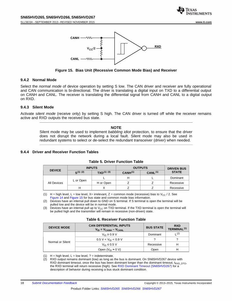
9.4.1 Can Bus StatesThe CAN bus has two states during powered operation of the device; dominant and recessive. A dominant busstate is when the bus is driven differentially, corresponding to a logic low on the TXD and RXD terminal. Arecessive bus state is when the bus is biased to VCC / 2 via the high-resistance internal input resistors RIN of thereceiver, corresponding to a logic high on the TXD and RXD terminals. See Figure 14 and Figure 15.
Figure 14. Bus States (Physical Bit Representation)
SN65HVD265, SN65HVD266, SN65HVD267SLLSEI3A –SEPTEMBER 2013–REVISED NOVEMBER 2015 www.ti.com
Figure 15. Bias Unit (Recessive Common Mode Bias) and Receiver
9.4.2 Normal ModeSelect the normal mode of device operation by setting S low. The CAN driver and receiver are fully operationaland CAN communication is bi-directional. The driver is translating a digital input on TXD to a differential outputon CANH and CANL. The receiver is translating the differential signal from CANH and CANL to a digital outputon RXD.
9.4.3 Silent ModeActivate silent mode (receive only) by setting S high. The CAN driver is turned off while the receiver remainsactive and RXD outputs the received bus state.
NOTESilent mode may be used to implement babbling idiot protection, to ensure that the driverdoes not disrupt the network during a local fault. Silent mode may also be used inredundant systems to select or de-select the redundant transceiver (driver) when needed.
9.4.4 Driver and Receiver Function Tables
Table 5. Driver Function TableINPUTS OUTPUTS DRIVEN BUSDEVICE STATES (1) (2) TXD (1) (3) CANH (1) CANL (1)
L H L DominantL or Open
All Devices H or Open Z Z RecessiveH X Z Z Recessive
(1) H = high level, L = low level, X= irrelevant, Z = common mode (recessive) bias to VCC / 2. SeeFigure 14 and Figure 15 for bus state and common mode bias information.
(2) Devices have an internal pull down to GND on S terminal. If S terminal is open the terminal will bepulled low and the device will be in normal mode.
(3) Devices have an internal pull up to VCC on TXD terminal. If the TXD terminal is open the terminal willbe pulled high and the transmitter will remain in recessive (non-driven) state.
Table 6. Receiver Function TableCAN DIFFERENTIAL INPUTS RXDDEVICE MODE BUS STATE TERMINAL (1)VID = VCANH – VCANL
VID ≥ 0.9 V Dominant L (2)
0.5 V < VID < 0.9 V ? ?Normal or Silent
VID ≤ 0.5 V Recessive HOpen (VID ≈ 0 V) Open H
(1) H = high level, L = low level, ? = indeterminate.(2) RXD output remains dominant (low) as long as the bus is dominant. On SN65HVD267 device with
RXD dominant timeout, once the bus has been dominant longer than the dominant timeout, tRXD_DTO,the RXD terminal will return recessive (high). See RXD Dominant Timeout (SN65HVD267) for adescription of behavior during receiving a bus stuck dominant condition.
SN65HVD265, SN65HVD266, SN65HVD267www.ti.com SLLSEI3A –SEPTEMBER 2013–REVISED NOVEMBER 2015
9.4.5 Digital Inputs and Outputs
9.4.5.1 5-V VCC Only Devices (SN65HVD265 and SN65HVD267)The 5-V VCC device is supplied by a single 5-V rail. The digital inputs are 5 V and 3.3 V compatible. This devicehas a 5-V (VCC) level RXD output. TXD is internally pulled up to VCC and S is internally pulled down to GND.
NOTETXD is internally pulled up to VCC and the S terminal is internally pulled down to GND.However, the internal bias may only put the device into a known state if the terminals float.The internal bias may be inadequate for system-level biasing. TXD pullup strength andCAN bit timing require special consideration when the SN65HVD26x devices are usedwith an open-drain TXD output on the CAN controller. An adequate external pullup resistormust be used to ensure that the CAN controller output of the μP maintains adequate bittiming input to the SN65HVD26x.
9.4.5.2 5-V VCC with VRXD RXD Output Supply Devices (SN65HVD266)This device is a 5-V VCC CAN transceiver with a separate supply for the RXD output, VRXD. The digital inputs are5 V and 3.3 V compatible. These devices have a VRXD-level RXD output. TXD remains weakly pulled up to VCC.
NOTEOn device versions with a VRXD supply that shifts the RXD output level, the input terminalsof the device remain the same. TXD remains weakly pulled up to VCC internally. Thus, asmall IIH current flows if the TXD input is used below VCC levels.
9.4.5.3 5-V VCC with FAULT Open-Drain Output Device (SN65HVD267)This device has a FAULT output terminal (open-drain). FAULT must be pulled up to VCC or I/O supply level viaan external resistor.
NOTEBecause the FAULT output terminal is open-drain, it actively pulls down when there is nofault, and becomes high-impedance when a fault condition is detected. An external pullupresistor to the VCC or I/O supply of the system must be used to pull the terminal high toindicate a fault to the host microprocessor. The open-drain architecture makes the faultterminal compatible with 3.3 V and 5 V I/O-level systems. The pullup current, selected bythe pullup resistance value, should be as low as possible while achieving the desiredvoltage level output in the system with margin against noise.
Typical CAN Transceiver Application Using 5V IO Connections
Typical CAN Transceiver Application Using 3.3V IO Connections
Optional: Filtering, Transient and ESD
SN65HVD265, SN65HVD266, SN65HVD267SLLSEI3A –SEPTEMBER 2013–REVISED NOVEMBER 2015 www.ti.com
10 Application and Implementation
NOTEInformation in the following applications sections is not part of the TI componentspecification, and TI does not warrant its accuracy or completeness. TI’s customers areresponsible for determining suitability of components for their purposes. Customers shouldvalidate and test their design implementation to confirm system functionality.
10.1 Application InformationThese CAN transceivers are typically used in applications with a host microprocessor or FPGA that includes thelink layer portion of the CAN protocol. Below are typical application configurations for both 5 V and 3.3 Vmicroprocessor applications. The bus termination is shown for illustrative purposes.
10.2.1.1 Bus Loading, Length and Number of NodesThe ISO11898 Standard specifies a maximum bus length of 40m and maximum stub length of 0.3m. However,with careful design, users can have longer cables, longer stub lengths, and many more nodes to a bus. A largenumber of nodes requires a transceiver with high input impedance such as the SN65HVD26x family.
Many CAN organizations and standards have scaled the use of CAN for applications outside the originalISO11898. They have made system level trade offs for data rate, cable length, and parasitic loading of the bus.Examples of some of these specifications are ARINC825, CANopen, DeviceNet and NMEA2000.
A CAN network design is a series of tradeoffs, but these devices operate over wide common-mode range. InISO11898-2 the driver differential output is specified with a 60Ω load (the two 120Ω termination resistors inparallel) and the differential output must be greater than 1.5V. The SN65HVD26x family is specified to meet the1.5V requirement with a 45Ω load incorporating the worst case including parallel transceivers. The differentialinput resistance of the SN65HVD26x is a minimum of 30KΩ. If 167 SN65HVD26x family transceivers are inparallel on a bus, this is equivalent to a 180Ω differential load worst case. That transceiver load of 180Ω inparallel with the 60Ω gives a total 45Ω. Therefore, the SN65HVD26x family theoretically supports over 167transceivers on a single bus segment with margin to the 1.2V minimum differential input at each node. Howeverfor CAN network design margin must be given for signal loss across the system and cabling, parasitic loadings,network imbalances, ground offsets and signal integrity thus a practical maximum number of nodes is typicallymuch lower. Bus length may also be extended beyond the original ISO11898 standard of 40m by careful systemdesign and datarate tradeoffs. For example CANopen network design guidelines allow the network to be up to1km with changes in the termination resistance, cabling, less than 64 nodes and significantly lowered data rate.
This flexibility in CAN network design is one of the key strengths of the various extensions and additionalstandards that have been built on the original ISO11898 CAN standard. In using this flexibility comes theresponsibility of good network design and balancing these tradeoffs.
10.2.2 Detailed Design Procedures
10.2.2.1 CAN TerminationThe ISO11898 standard specifies the interconnect to be a twisted pair cable (shielded or unshielded) with 120 Ωcharacteristic impedance (ZO). Resistors equal to the characteristic impedance of the line should be used toterminate both ends of the cable to prevent signal reflections. Unterminated drop lines (stubs) connecting nodesto the bus should be kept as short as possible to minimize signal reflections. The termination may be on thecable or in a node, but if nodes may be removed from the bus the termination must be carefully placed so that itis not removed from the bus.
SN65HVD265, SN65HVD266, SN65HVD267SLLSEI3A –SEPTEMBER 2013–REVISED NOVEMBER 2015 www.ti.com
Typical Application (continued)Termination may be a single 120 Ω resistor at the end of the bus, either on the cable or in a terminating node. Iffiltering and stabilization of the common mode voltage of the bus is desired, then split termination may be used.(See Figure 18). Split termination improves the electromagnetic emissions behavior of the network by eliminatingfluctuations in the bus common-mode voltages at the start and end of message transmissions.
Figure 18. CAN Bus Termination Concepts
10.2.2.2 Functional Safety Using the SN65HVD267 in a Redundant Physical Layer CAN NetworkTopology
CAN is a standard linear bus topology using 120 Ω twisted pair cabling. The SN65HVD267 CAN device includesseveral features to use the CAN physical layer in nonstandard topologies with only one CAN link layer controller(μP) interface. This allows much greater flexibility in the physical topology of the bus while reducing the digitalcontroller and software costs. The combination of RXD DTO and the FAULT output allows great flexibility, controland monitoring of these applications.
A simple example of this flexibility is to use two SN65HVD267 devices in parallel with an AND gate to achieveredundancy (parallel) of the physical layer (cabling and PHYs) in a CAN network.
For the CAN bit-wise arbitration to work, the RXD outputs of the transceivers must connect via AND gate logic sothat a dominant bit (low) from any of the branches is received by the link layer logic (μP), and appears to the linklayer and above as a single physical network. The RXD DTO feature prevents a bus stuck dominant fault in asingle branch from taking down the entire network by forcing the RXD terminal for the transceivers on the branchwith the fault back to the recessive after the tRXD_DTO time. The remaining branch of the network continues tofunction. The FAULT terminal of the transceivers on the branch with the fault indicates this via the FAULT outputto their host processors, which diagnose the failure condition. Adding a logic XOR with a filter adds automaticdetection for a fault where one of the 2 networks goes open (recessive) in addition to the faults detected by theSN65HVD267. The S terminal (silent mode terminal) may be used to put a branch in silent mode to check eachbranch for other faults. Thus it is possible to implement a robust and redundant CAN network topology in asimple and low cost manner.
These concepts can be expanded into more complicated and flexible CAN network topologies to solve varioussystem level challenges with a networked infrastructure.
SN65HVD265, SN65HVD266, SN65HVD267www.ti.com SLLSEI3A –SEPTEMBER 2013–REVISED NOVEMBER 2015
Typical Application (continued)
A. CAN nodes with termination are PHY 1A, PHY 2A, PHY 1Z and PHY 2Z.B. RXD DTO prevents a single branch-stuck-dominant condition from blocking the redundant branch via the AND logic
on RXD. The transceivers signal a received bus stuck dominant fault via the FAULT terminal. The system detectswhich branch is stuck dominant, and issues a system warning. Other network faults on a single branch that appear asrecessive (not blocking the redundant network) may be detected through a logic XOR with a filter and diagnosticroutines, and using the Silent Mode of the PHYs to use only one branch at a time for transmission during diagnosticmode. This combination allows robust fault detection and recovery within single branches so that they may berepaired and again provide redundancy of the physical layer.
Figure 19. Typical Redundant Physical Layer Topology Using the SN65HVD267
10.2.3 Application Curve
Figure 20. Typical CAN Transceiver Operation Using 3.3V IO Connections
SN65HVD265, SN65HVD266, SN65HVD267SLLSEI3A –SEPTEMBER 2013–REVISED NOVEMBER 2015 www.ti.com
11 Power Supply Recommendations
These devices are designed to operate from main VCC input voltage supply range between 4.5 V and 5.5 V.Some devices have an output level shifting supply input, VRXD, designed for a range between 2.8 V and 5.5 V.Both supply inputs must be well regulated. A bulk capacitance, typically 4.7 μF, should be placed near the CANtransceiver's main VCC supply terminal in addition to bypass capacitors. A bulk capacitance, typically 1 μF,should be placed near the CAN transceiver's VRXD supply terminal in addition to bypass capacitors.
12 Layout
12.1 Layout GuidelinesFor the PCB design to be successful, start with design of the protection and filtering circuitry. Because ESD andEFT transients have a wide frequency bandwidth from approximately 3 MHz to 3 GHz, high frequency layouttechniques must be applied during PCB design. On chip IEC ESD protection is good for laboratory and portableequipment but is usually not sufficient for EFT and surge transients occurring in industrial environments.Therefore, robust and reliable bus node design requires the use of external transient protection devices at thebus connectors. Placement at the connector also prevents these noisy events from propagating further into thePCB and system.• Place the protection and filtering circuitry as close to the bus connector, J1, to prevent transients, ESD and
noise from penetrating onto the board. In this layout example for protection a Transient Voltage Suppression(TVS) device, D1, has been used. The production solution can be either bi-directional TVS diode or varistorwith ratings matching the application requirements. This example also shows optional bus filter capacitors C8and C9.
• Design the bus protection components in the direction of the signal path. Do not force the transient current todivert from the signal path to reach the protection device.
• Use supply (VCC) and ground planes to provide low inductance. Note: high frequency current follows the pathof least inductance and not the path of least impedance.
• Use at least two vias for supply (VCC) and ground connections of bypass capacitors and protection devices tominimize trace and via inductance.
• Bypass and bulk capacitors should be placed as close as possible to the supply terminals of transceiver,examples C2, C3 (VCC) and for the dual supply devices additionally C5 and C6 (VRXD).
• Bus termination: this layout example shows split termination. This is where the termination is split into tworesistors, R7 and R8, with the center or split tap of the termination connected to ground via capacitor C7. Splittermination provides common mode filtering for the bus. When bus termination is placed on the board insteadof directly on the bus, additional care must be taken to ensure the terminating node is not removed from thebus thus also removing the termination. See the application section for information on power ratings neededfor the termination resistor(s).
• To limit current of digital lines serial resistors may be used. Examples are R2, R3, R4 and R5.• To filter noise on the digital IO lines a capacitor may be used close to the input side of the IO as shown by C1
and C4.• Terminal 5: This example is showing a flexible layout covering all three of the devices in this CAN transceiver
family on terminal 5. SN65HVD265: this terminal is a no connect so external connections are un-importantand the components R4, R5, C5 and C6 do not matter. SN65HVD266: this terminal is the RXD output supplyterminal, VRXD. The bypass and bulk capacitor pads of C5 and C6 should be populated and R5 and R6 arenot used. SN65HVD267: this terminal is the FAULT output (open drain). The pull resistor R6 is needed. R5 isshown if current limiting is desired to the host processor. If noise filtering is desired C5 should be used.
• 1k to 10kΩ pull-up or down resistors should be used where required to limit noise during transient events.• Terminal 1: R1 is shown optionally for the TXD input of the device. If an option drain host processor is used
this is mandatory to ensure the bit timing into the device is met.• Terminal 8: is shown assuming the mode terminal, S, will be used. If the device will only be used in normal
mode R3 is not needed and the pads of C4 could be used for the pull down resistor to GND.
SN65HVD265, SN65HVD266, SN65HVD267SLLSEI3A –SEPTEMBER 2013–REVISED NOVEMBER 2015 www.ti.com
13 Device and Documentation Support
13.1 Related LinksThe table below lists quick access links. Categories include technical documents, support and communityresources, tools and software, and quick access to sample or buy.
Table 7. Related LinksTECHNICAL TOOLS & SUPPORT &PARTS PRODUCT FOLDER SAMPLE & BUY DOCUMENTS SOFTWARE COMMUNITY
SN65HVD265 Click here Click here Click here Click here Click hereSN65HVD266 Click here Click here Click here Click here Click hereSN65HVD267 Click here Click here Click here Click here Click here
13.2 Community ResourcesThe following links connect to TI community resources. Linked contents are provided "AS IS" by the respectivecontributors. They do not constitute TI specifications and do not necessarily reflect TI's views; see TI's Terms ofUse.
TI E2E™ Online Community TI's Engineer-to-Engineer (E2E) Community. Created to foster collaborationamong engineers. At e2e.ti.com, you can ask questions, share knowledge, explore ideas and helpsolve problems with fellow engineers.
Design Support TI's Design Support Quickly find helpful E2E forums along with design support tools andcontact information for technical support.
13.3 TrademarksE2E is a trademark of Texas Instruments.All other trademarks are the property of their respective owners.
13.4 Electrostatic Discharge CautionThese devices have limited built-in ESD protection. The leads should be shorted together or the device placed in conductive foamduring storage or handling to prevent electrostatic damage to the MOS gates.
13.5 GlossarySLYZ022 — TI Glossary.
This glossary lists and explains terms, acronyms, and definitions.
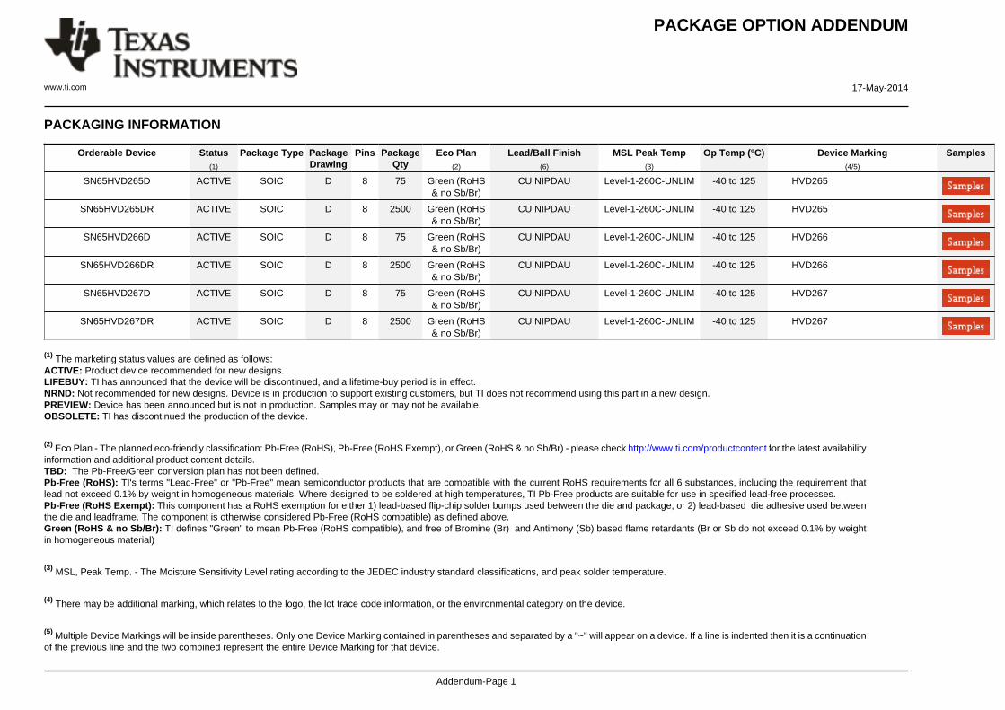
14 Mechanical, Packaging, and Orderable InformationThe following pages include mechanical packaging and orderable information. This information is the mostcurrent data available for the designated devices. This data is subject to change without notice and revision ofthis document. For browser-based versions of this data sheet, refer to the left-hand navigation.
SN65HVD265D ACTIVE SOIC D 8 75 Green (RoHS& no Sb/Br)
CU NIPDAU Level-1-260C-UNLIM -40 to 125 HVD265
SN65HVD265DR ACTIVE SOIC D 8 2500 Green (RoHS& no Sb/Br)
CU NIPDAU Level-1-260C-UNLIM -40 to 125 HVD265
SN65HVD266D ACTIVE SOIC D 8 75 Green (RoHS& no Sb/Br)
CU NIPDAU Level-1-260C-UNLIM -40 to 125 HVD266
SN65HVD266DR ACTIVE SOIC D 8 2500 Green (RoHS& no Sb/Br)
CU NIPDAU Level-1-260C-UNLIM -40 to 125 HVD266
SN65HVD267D ACTIVE SOIC D 8 75 Green (RoHS& no Sb/Br)
CU NIPDAU Level-1-260C-UNLIM -40 to 125 HVD267
SN65HVD267DR ACTIVE SOIC D 8 2500 Green (RoHS& no Sb/Br)
CU NIPDAU Level-1-260C-UNLIM -40 to 125 HVD267
(1) The marketing status values are defined as follows:ACTIVE: Product device recommended for new designs.LIFEBUY: TI has announced that the device will be discontinued, and a lifetime-buy period is in effect.NRND: Not recommended for new designs. Device is in production to support existing customers, but TI does not recommend using this part in a new design.PREVIEW: Device has been announced but is not in production. Samples may or may not be available.OBSOLETE: TI has discontinued the production of the device.
(2) Eco Plan - The planned eco-friendly classification: Pb-Free (RoHS), Pb-Free (RoHS Exempt), or Green (RoHS & no Sb/Br) - please check http://www.ti.com/productcontent for the latest availabilityinformation and additional product content details.TBD: The Pb-Free/Green conversion plan has not been defined.Pb-Free (RoHS): TI's terms "Lead-Free" or "Pb-Free" mean semiconductor products that are compatible with the current RoHS requirements for all 6 substances, including the requirement thatlead not exceed 0.1% by weight in homogeneous materials. Where designed to be soldered at high temperatures, TI Pb-Free products are suitable for use in specified lead-free processes.Pb-Free (RoHS Exempt): This component has a RoHS exemption for either 1) lead-based flip-chip solder bumps used between the die and package, or 2) lead-based die adhesive used betweenthe die and leadframe. The component is otherwise considered Pb-Free (RoHS compatible) as defined above.Green (RoHS & no Sb/Br): TI defines "Green" to mean Pb-Free (RoHS compatible), and free of Bromine (Br) and Antimony (Sb) based flame retardants (Br or Sb do not exceed 0.1% by weightin homogeneous material)
(3) MSL, Peak Temp. - The Moisture Sensitivity Level rating according to the JEDEC industry standard classifications, and peak solder temperature.
(4) There may be additional marking, which relates to the logo, the lot trace code information, or the environmental category on the device.
(5) Multiple Device Markings will be inside parentheses. Only one Device Marking contained in parentheses and separated by a "~" will appear on a device. If a line is indented then it is a continuationof the previous line and the two combined represent the entire Device Marking for that device.
(6) Lead/Ball Finish - Orderable Devices may have multiple material finish options. Finish options are separated by a vertical ruled line. Lead/Ball Finish values may wrap to two lines if the finishvalue exceeds the maximum column width.
Important Information and Disclaimer:The information provided on this page represents TI's knowledge and belief as of the date that it is provided. TI bases its knowledge and belief on informationprovided by third parties, and makes no representation or warranty as to the accuracy of such information. Efforts are underway to better integrate information from third parties. TI has taken andcontinues to take reasonable steps to provide representative and accurate information but may not have conducted destructive testing or chemical analysis on incoming materials and chemicals.TI and TI suppliers consider certain information to be proprietary, and thus CAS numbers and other limited information may not be available for release.
In no event shall TI's liability arising out of such information exceed the total purchase price of the TI part(s) at issue in this document sold by TI to Customer on an annual basis.
Texas Instruments Incorporated (TI) reserves the right to make corrections, enhancements, improvements and other changes to itssemiconductor products and services per JESD46, latest issue, and to discontinue any product or service per JESD48, latest issue. Buyersshould obtain the latest relevant information before placing orders and should verify that such information is current and complete.TI’s published terms of sale for semiconductor products (http://www.ti.com/sc/docs/stdterms.htm) apply to the sale of packaged integratedcircuit products that TI has qualified and released to market. Additional terms may apply to the use or sale of other types of TI products andservices.Reproduction of significant portions of TI information in TI data sheets is permissible only if reproduction is without alteration and isaccompanied by all associated warranties, conditions, limitations, and notices. TI is not responsible or liable for such reproduceddocumentation. Information of third parties may be subject to additional restrictions. Resale of TI products or services with statementsdifferent from or beyond the parameters stated by TI for that product or service voids all express and any implied warranties for theassociated TI product or service and is an unfair and deceptive business practice. TI is not responsible or liable for any such statements.Buyers and others who are developing systems that incorporate TI products (collectively, “Designers”) understand and agree that Designersremain responsible for using their independent analysis, evaluation and judgment in designing their applications and that Designers havefull and exclusive responsibility to assure the safety of Designers' applications and compliance of their applications (and of all TI productsused in or for Designers’ applications) with all applicable regulations, laws and other applicable requirements. Designer represents that, withrespect to their applications, Designer has all the necessary expertise to create and implement safeguards that (1) anticipate dangerousconsequences of failures, (2) monitor failures and their consequences, and (3) lessen the likelihood of failures that might cause harm andtake appropriate actions. Designer agrees that prior to using or distributing any applications that include TI products, Designer willthoroughly test such applications and the functionality of such TI products as used in such applications.TI’s provision of technical, application or other design advice, quality characterization, reliability data or other services or information,including, but not limited to, reference designs and materials relating to evaluation modules, (collectively, “TI Resources”) are intended toassist designers who are developing applications that incorporate TI products; by downloading, accessing or using TI Resources in anyway, Designer (individually or, if Designer is acting on behalf of a company, Designer’s company) agrees to use any particular TI Resourcesolely for this purpose and subject to the terms of this Notice.TI’s provision of TI Resources does not expand or otherwise alter TI’s applicable published warranties or warranty disclaimers for TIproducts, and no additional obligations or liabilities arise from TI providing such TI Resources. TI reserves the right to make corrections,enhancements, improvements and other changes to its TI Resources. TI has not conducted any testing other than that specificallydescribed in the published documentation for a particular TI Resource.Designer is authorized to use, copy and modify any individual TI Resource only in connection with the development of applications thatinclude the TI product(s) identified in such TI Resource. NO OTHER LICENSE, EXPRESS OR IMPLIED, BY ESTOPPEL OR OTHERWISETO ANY OTHER TI INTELLECTUAL PROPERTY RIGHT, AND NO LICENSE TO ANY TECHNOLOGY OR INTELLECTUAL PROPERTYRIGHT OF TI OR ANY THIRD PARTY IS GRANTED HEREIN, including but not limited to any patent right, copyright, mask work right, orother intellectual property right relating to any combination, machine, or process in which TI products or services are used. Informationregarding or referencing third-party products or services does not constitute a license to use such products or services, or a warranty orendorsement thereof. Use of TI Resources may require a license from a third party under the patents or other intellectual property of thethird party, or a license from TI under the patents or other intellectual property of TI.TI RESOURCES ARE PROVIDED “AS IS” AND WITH ALL FAULTS. TI DISCLAIMS ALL OTHER WARRANTIES ORREPRESENTATIONS, EXPRESS OR IMPLIED, REGARDING RESOURCES OR USE THEREOF, INCLUDING BUT NOT LIMITED TOACCURACY OR COMPLETENESS, TITLE, ANY EPIDEMIC FAILURE WARRANTY AND ANY IMPLIED WARRANTIES OFMERCHANTABILITY, FITNESS FOR A PARTICULAR PURPOSE, AND NON-INFRINGEMENT OF ANY THIRD PARTY INTELLECTUALPROPERTY RIGHTS. TI SHALL NOT BE LIABLE FOR AND SHALL NOT DEFEND OR INDEMNIFY DESIGNER AGAINST ANY CLAIM,INCLUDING BUT NOT LIMITED TO ANY INFRINGEMENT CLAIM THAT RELATES TO OR IS BASED ON ANY COMBINATION OFPRODUCTS EVEN IF DESCRIBED IN TI RESOURCES OR OTHERWISE. IN NO EVENT SHALL TI BE LIABLE FOR ANY ACTUAL,DIRECT, SPECIAL, COLLATERAL, INDIRECT, PUNITIVE, INCIDENTAL, CONSEQUENTIAL OR EXEMPLARY DAMAGES INCONNECTION WITH OR ARISING OUT OF TI RESOURCES OR USE THEREOF, AND REGARDLESS OF WHETHER TI HAS BEENADVISED OF THE POSSIBILITY OF SUCH DAMAGES.Unless TI has explicitly designated an individual product as meeting the requirements of a particular industry standard (e.g., ISO/TS 16949and ISO 26262), TI is not responsible for any failure to meet such industry standard requirements.Where TI specifically promotes products as facilitating functional safety or as compliant with industry functional safety standards, suchproducts are intended to help enable customers to design and create their own applications that meet applicable functional safety standardsand requirements. Using products in an application does not by itself establish any safety features in the application. Designers mustensure compliance with safety-related requirements and standards applicable to their applications. Designer may not use any TI products inlife-critical medical equipment unless authorized officers of the parties have executed a special contract specifically governing such use.Life-critical medical equipment is medical equipment where failure of such equipment would cause serious bodily injury or death (e.g., lifesupport, pacemakers, defibrillators, heart pumps, neurostimulators, and implantables). Such equipment includes, without limitation, allmedical devices identified by the U.S. Food and Drug Administration as Class III devices and equivalent classifications outside the U.S.TI may expressly designate certain products as completing a particular qualification (e.g., Q100, Military Grade, or Enhanced Product).Designers agree that it has the necessary expertise to select the product with the appropriate qualification designation for their applicationsand that proper product selection is at Designers’ own risk. Designers are solely responsible for compliance with all legal and regulatoryrequirements in connection with such selection.Designer will fully indemnify TI and its representatives against any damages, costs, losses, and/or liabilities arising out of Designer’s non-compliance with the terms and provisions of this Notice.