SN74F161A SYNCHRONOUS 4-BIT BINARY COUNTER SDFS056B – MARCH 1987 – REVISED AUGUST 2001 1 POST OFFICE BOX 655303 • DALLAS, TEXAS 75265 Internal Look-Ahead Circuitry for Fast Counting Carry Output for N-Bit Cascading Fully Synchronous Operation for Counting description This synchronous, presettable, 4-bit binary counter has internal carry look-ahead circuitry for use in high-speed counting designs. Synchronous operation is provided by having all flip-flops clocked simultaneously so that the outputs change coincident with each other when so instructed by the count-enable (ENP, ENT) inputs and internal gating. This mode of operation eliminates the output counting spikes that are normally associated with asynchronous (ripple-clock) counters. However, counting spikes can occur on the ripple-carry (RCO) output. A buffered clock (CLK) input triggers the four flip-flops on the rising (positive-going) edge of CLK. This counter is fully programmable. That is, it can be preset to any number between 0 and 15. Because presetting is synchronous, a low logic level at the load (LOAD ) input disables the counter and causes the outputs to agree with the setup data after the next clock pulse, regardless of the levels of ENP and ENT. The clear function is asynchronous, and a low logic level at the clear (CLR ) input sets all four of the flip-flop outputs to low, regardless of the levels of CLK, LOAD , ENP, and ENT. The carry look-ahead circuitry provides for cascading counters for n-bit synchronous applications, without additional gating. This function is implemented by the ENP and ENT inputs and an RCO output. Both ENP and ENT must be high to count, and ENT is fed forward to enable RCO. RCO, thus enabled, produces a high-logic-level pulse while the count is 15 (HHHH). The high-logic-level overflow ripple-carry pulse can be used to enable successive cascaded stages. Transitions at ENP or ENT are allowed, regardless of the level of CLK. The SN74F161A features a fully independent clock circuit. Changes at ENP, ENT, or LOAD that modify the operating mode have no effect on the contents of the counter until clocking occurs. The function of the counter (whether enabled, disabled, loading, or counting) is dictated solely by the conditions meeting the setup and hold times. ORDERING INFORMATION T A PACKAGE † ORDERABLE PART NUMBER TOP-SIDE MARKING PDIP – N Tube SN74F161AN SN74F161AN 0°C to 70°C SOIC D Tube SN74F161AD F161A 0°C to 70°C SOIC – D Tape and reel SN74F161ADR F161A SSOP – DB Tape and reel SN74F161ADBR F161A † Package drawings, standard packing quantities, thermal data, symbolization, and PCB design guidelines are available at www.ti.com/sc/package. Copyright 2001, Texas Instruments Incorporated PRODUCTION DATA information is current as of publication date. Products conform to specifications per the terms of Texas Instruments standard warranty. Production processing does not necessarily include testing of all parameters. Please be aware that an important notice concerning availability, standard warranty, and use in critical applications of Texas Instruments semiconductor products and disclaimers thereto appears at the end of this data sheet. 1 2 3 4 5 6 7 8 16 15 14 13 12 11 10 9 CLR CLK A B C D ENP GND V CC RCO Q A Q B Q C Q D ENT LOAD D, DB, OR N PACKAGE (TOP VIEW)
Transcript
SN74F161ASYNCHRONOUS 4-BIT BINARY COUNTER
SDFS056B – MARCH 1987 – REVISED AUGUST 2001
1POST OFFICE BOX 655303 • DALLAS, TEXAS 75265
Internal Look-Ahead Circuitry for FastCounting
Carry Output for N-Bit Cascading
Fully Synchronous Operation for Counting
description
This synchronous, presettable, 4-bit binarycounter has internal carry look-ahead circuitryfor use in high-speed counting designs.Synchronous operation is provided by having allflip-flops clocked simultaneously so that theoutputs change coincident with each other whenso instructed by the count-enable (ENP, ENT) inputs and internal gating. This mode of operation eliminates theoutput counting spikes that are normally associated with asynchronous (ripple-clock) counters. However,counting spikes can occur on the ripple-carry (RCO) output. A buffered clock (CLK) input triggers the fourflip-flops on the rising (positive-going) edge of CLK.
This counter is fully programmable. That is, it can be preset to any number between 0 and 15. Becausepresetting is synchronous, a low logic level at the load (LOAD) input disables the counter and causes the outputsto agree with the setup data after the next clock pulse, regardless of the levels of ENP and ENT.
The clear function is asynchronous, and a low logic level at the clear (CLR) input sets all four of the flip-flopoutputs to low, regardless of the levels of CLK, LOAD, ENP, and ENT.
The carry look-ahead circuitry provides for cascading counters for n-bit synchronous applications, withoutadditional gating. This function is implemented by the ENP and ENT inputs and an RCO output. Both ENP andENT must be high to count, and ENT is fed forward to enable RCO. RCO, thus enabled, produces ahigh-logic-level pulse while the count is 15 (HHHH). The high-logic-level overflow ripple-carry pulse can be usedto enable successive cascaded stages. Transitions at ENP or ENT are allowed, regardless of the level of CLK.
The SN74F161A features a fully independent clock circuit. Changes at ENP, ENT, or LOAD that modify theoperating mode have no effect on the contents of the counter until clocking occurs. The function of the counter(whether enabled, disabled, loading, or counting) is dictated solely by the conditions meeting the setup and holdtimes.
ORDERING INFORMATION
TA PACKAGE† ORDERABLEPART NUMBER
TOP-SIDEMARKING
PDIP – N Tube SN74F161AN SN74F161AN
0°C to 70°C SOIC DTube SN74F161AD
F161A0°C to 70°C SOIC – DTape and reel SN74F161ADR
F161A
SSOP – DB Tape and reel SN74F161ADBR F161A
† Package drawings, standard packing quantities, thermal data, symbolization, and PCB design guidelinesare available at www.ti.com/sc/package.
Copyright 2001, Texas Instruments IncorporatedPRODUCTION DATA information is current as of publication date.Products conform to specifications per the terms of Texas Instrumentsstandard warranty. Production processing does not necessarily includetesting of all parameters.
Please be aware that an important notice concerning availability, standard warranty, and use in critical applications ofTexas Instruments semiconductor products and disclaimers thereto appears at the end of this data sheet.
1
2
3
4
5
6
7
8
16
15
14
13
12
11
10
9
CLRCLK
ABCD
ENPGND
VCCRCOQAQBQCQDENTLOAD
D, DB, OR N PACKAGE(TOP VIEW)
SN74F161ASYNCHRONOUS 4-BIT BINARY COUNTER
SDFS056B – MARCH 1987 – REVISED AUGUST 2001
2 POST OFFICE BOX 655303 • DALLAS, TEXAS 75265
state diagram
0
15
14
13
12
1 2 3 4
5
6
7
891011
SN74F161ASYNCHRONOUS 4-BIT BINARY COUNTER
SDFS056B – MARCH 1987 – REVISED AUGUST 2001
3POST OFFICE BOX 655303 • DALLAS, TEXAS 75265
logic diagram (positive logic)
R
G2
1, 3D
M1
1, 2T/C3
R
G2
1, 3D
M1
1, 2T/C3
R
G2
1, 3D
M1
1, 2T/C3
R
G2
1, 3D
M1
1, 2T/C3
1
9
10
7
2
3
4
5
6
15
14
13
12
11
CLR
LOAD
ENT
ENP
CLK
A
B
C
D
RCO
QA
QB
QC
QD
SN74F161ASYNCHRONOUS 4-BIT BINARY COUNTER
SDFS056B – MARCH 1987 – REVISED AUGUST 2001
4 POST OFFICE BOX 655303 • DALLAS, TEXAS 75265
logic symbol, each flip-flop
R
G2TEQ1
1, 3DD
M1LOAD
Q21, 2T/C3
R
CLK
Q1
Q2
logic diagram, each flip-flop (positive logic)
R
CLK
D
LOAD
TE(ToggleEnable) Q1
Q2
SN74F161ASYNCHRONOUS 4-BIT BINARY COUNTER
SDFS056B – MARCH 1987 – REVISED AUGUST 2001
5POST OFFICE BOX 655303 • DALLAS, TEXAS 75265
typical clear, preset, count, and inhibit sequences
The following timing sequence is illustrated below:
1. Clear outputs to zero
2. Preset to binary 12
3. Count to 13, 14, 15, 0, 1, and 2
4. Inhibit
DataInputs
DataOutputs
CLR
LOAD
A
B
C
D
CLK
ENP
ENT
RCO
QA
QB
QC
QD
AsyncClear
SyncClear
Preset
Count Inhibit
12 13 14 15 0 1 2
SN74F161ASYNCHRONOUS 4-BIT BINARY COUNTER
SDFS056B – MARCH 1987 – REVISED AUGUST 2001
6 POST OFFICE BOX 655303 • DALLAS, TEXAS 75265
absolute maximum ratings over operating free-air temperature range (unless otherwise noted)†
† Stresses beyond those listed under “absolute maximum ratings” may cause permanent damage to the device. These are stress ratings only, andfunctional operation of the device at these or any other conditions beyond those indicated under “recommended operating conditions” is notimplied. Exposure to absolute-maximum-rated conditions for extended periods may affect device reliability.
NOTES: 1. The input voltage ratings may be exceeded provided the input current ratings are observed.2. The package thermal impedance is calculated in accordance with JESD 51-7.
recommended operating conditions (see Note 3)
MIN NOM MAX UNIT
VCC Supply voltage 4.5 5 5.5 V
VIH High-level input voltage 2 V
VIL Low-level input voltage 0.8 V
IIK Input clamp current –18 mA
IOH High-level output current –1 mA
IOL Low-level output current 20 mA
TA Operating free-air temperature 0 70 °C
NOTE 3: All unused inputs of the device must be held at VCC or GND to ensure proper device operation. Refer to the TI application report,Implications of Slow or Floating CMOS Inputs, literature number SCBA004.
electrical characteristics over recommended operating free-air temperature range (unlessotherwise noted)
PARAMETER TEST CONDITIONS MIN TYP‡ MAX UNIT
VIK VCC = 4.5 V, II = –18 mA –1.2 V
VOHVCC = 4.5 V, IOH = – 1 mA 2.5 3.4
VVOHVCC = 4.75 V, IOH = – 1 mA 2.7
V
VOL VCC = 4.5 V, IOL = 20 mA 0.3 0.5 V
II VCC = 5.5 V, VI = 7 V 0.1 mA
IIH VCC = 5.5 V, VI = 2.7 V 20 µA
ENP, CLK, A, B, C, D – 0.6
IIL ENT, LOAD VCC = 5.5 V, VI = 0.5 V – 1.2 mA
CLR – 0.6
IOS§ VCC = 5.5 V, VO = 0 –60 –150 mA
ICC VCC = 5.5 V 37 55 mA
‡ All typical values are at VCC = 5 V, TA = 25°C.§ Not more than one output should be shorted at a time, and the duration of the short circuit should not exceed one second.
SN74F161ASYNCHRONOUS 4-BIT BINARY COUNTER
SDFS056B – MARCH 1987 – REVISED AUGUST 2001
7POST OFFICE BOX 655303 • DALLAS, TEXAS 75265
timing requirements over recommended ranges of supply voltage and operating free-airtemperature (unless otherwise noted)
VCC = 5 V,TA = 25°C MIN MAX UNITMIN MAX
fclock Clock frequency 0 100 0 90 MHz
CLK high or low (loading) 5 5
t Pulse duration CLK (counting)High 4 4
nstw Pulse duration CLK (counting)Low 6 7
ns
CLR low 5 5
Data before CLK↑ High or low 5 5
LOAD before CLK↑High 11 11.5
tsu Setup timeLOAD before CLK↑
Low 8.5 9.5 ns
ENP and ENT before CLK↑High 11 11.5
ENP and ENT before CLK↑Low 5 5
Data after CLK↑ High or low 2 2
th Hold time LOAD after CLK↑High 2 2
nsth Hold time LOAD after CLK↑Low 0 0
ns
ENP and ENT after CLK↑ High or low 0 0
tsu Inactive-state setup time, CLR high before CLK↑† 6 6 ns
† Inactive-state setup time also is referred to as recovery time.
switching characteristics (see Note 4)
PARAMETERFROM
(INPUT)TO
(OUTPUT)
VCC = 5 V,CL = 50 PF,RL = 500 Ω,TA = 25°C
VCC = 4.5 V TO 5.5 V,CL = 50 PF,RL = 500Ω,
TA = MIN TO MAX‡UNIT
MIN TYP MAX MIN MAX
fmax 100 120 90 MHz
tPLHCLK (LOAD high) Any Q
2.7 5.1 7.5 2.7 8.5ns
tPHLCLK (LOAD high) Any Q
2.7 7.1 10 2.7 11ns
tPLHCLK (LOAD low) Any Q
3.2 5.6 8.5 3.2 9.5ns
tPHLCLK (LOAD low) Any Q
3.2 5.6 8.5 3.2 9.5ns
tPLHCLK RCO
4.2 9.6 14 4.2 15ns
tPHLCLK RCO
4.2 9.6 14 4.2 15ns
tPLHENT RCO
1.7 4.1 7.5 1.7 8.5ns
tPHLENT RCO
1.7 4.1 7.5 1.7 8.5ns
tPHL CLRAny Q 4.7 8.6 12 4.7 13
nstPHL CLRRCO 3.7 7.6 10.5 3.7 11.5
ns
‡ For conditions shown as MIN or MAX, use the appropriate value specified under recommended operating conditions.NOTE 4: Load circuits and waveforms are shown in Figure 1.
SN74F161ASYNCHRONOUS 4-BIT BINARY COUNTER
SDFS056B – MARCH 1987 – REVISED AUGUST 2001
8 POST OFFICE BOX 655303 • DALLAS, TEXAS 75265
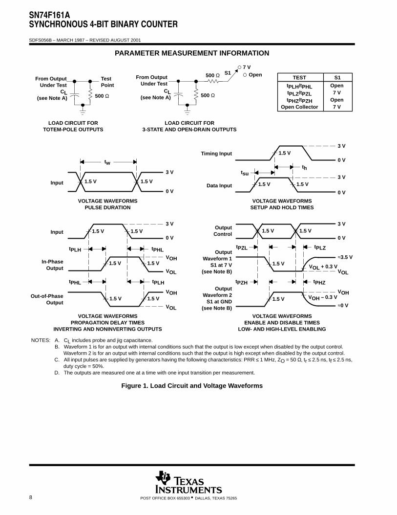
PARAMETER MEASUREMENT INFORMATION
3 V
3 V
0 V
0 V
thtsu
VOLTAGE WAVEFORMSSETUP AND HOLD TIMES
Data Input
tPLH
tPHL
tPHL
tPLH
VOH
VOH
VOL
VOL
3 V
0 VInput
Out-of-PhaseOutput
In-PhaseOutput
Timing Input
VOLTAGE WAVEFORMSPROPAGATION DELAY TIMES
INVERTING AND NONINVERTING OUTPUTS
OutputControl
OutputWaveform 1
S1 at 7 V(see Note B)
OutputWaveform 2
S1 at GND(see Note B)
VOL
VOH
tPZL
tPZH
tPLZ
tPHZ
≈3.5 V
0 V
VOL + 0.3 V
≈0 V
3 V
VOLTAGE WAVEFORMSENABLE AND DISABLE TIMES
LOW- AND HIGH-LEVEL ENABLING
tPLH/tPHLtPLZ/tPZLtPHZ/tPZH
Open Collector
Open7 V
Open7 V
TEST S1
3 V
0 V
tw
VOLTAGE WAVEFORMSPULSE DURATION
Input
NOTES: A. CL includes probe and jig capacitance.B. Waveform 1 is for an output with internal conditions such that the output is low except when disabled by the output control.
Waveform 2 is for an output with internal conditions such that the output is high except when disabled by the output control.C. All input pulses are supplied by generators having the following characteristics: PRR ≤ 1 MHz, ZO = 50 Ω, tr ≤ 2.5 ns, tf ≤ 2.5 ns,
duty cycle = 50%.D. The outputs are measured one at a time with one input transition per measurement.
From OutputUnder Test
CL(see Note A)
LOAD CIRCUIT FOR3-STATE AND OPEN-DRAIN OUTPUTS
S17 V
500 ΩFrom Output
Under TestCL
(see Note A)
TestPoint
LOAD CIRCUIT FORTOTEM-POLE OUTPUTS
Open
VOH – 0.3 V
500 Ω500 Ω
1.5 V 1.5 V
1.5 V 1.5 V
1.5 V 1.5 V
1.5 V 1.5 V
1.5 V1.5 V
1.5 V
1.5 V 1.5 V
1.5 V
1.5 V
Figure 1. Load Circuit and Voltage Waveforms
PACKAGE OPTION ADDENDUM
www.ti.com 14-Aug-2021
Addendum-Page 1
PACKAGING INFORMATION
Orderable Device Status(1)
Package Type PackageDrawing
Pins PackageQty
Eco Plan(2)
Lead finish/Ball material
(6)
MSL Peak Temp(3)
Op Temp (°C) Device Marking(4/5)
Samples
SN74F161AD ACTIVE SOIC D 16 40 RoHS & Green NIPDAU Level-1-260C-UNLIM 0 to 70 F161A
SN74F161ADR ACTIVE SOIC D 16 2500 RoHS & Green NIPDAU Level-1-260C-UNLIM 0 to 70 F161A
SN74F161AN ACTIVE PDIP N 16 25 RoHS & Green NIPDAU N / A for Pkg Type 0 to 70 SN74F161AN
SN74F161ANE4 ACTIVE PDIP N 16 25 RoHS & Green NIPDAU N / A for Pkg Type 0 to 70 SN74F161AN
SN74F161ANSR ACTIVE SO NS 16 2000 RoHS & Green NIPDAU Level-1-260C-UNLIM 0 to 70 74F161A
(1) The marketing status values are defined as follows:ACTIVE: Product device recommended for new designs.LIFEBUY: TI has announced that the device will be discontinued, and a lifetime-buy period is in effect.NRND: Not recommended for new designs. Device is in production to support existing customers, but TI does not recommend using this part in a new design.PREVIEW: Device has been announced but is not in production. Samples may or may not be available.OBSOLETE: TI has discontinued the production of the device.
(2) RoHS: TI defines "RoHS" to mean semiconductor products that are compliant with the current EU RoHS requirements for all 10 RoHS substances, including the requirement that RoHS substancedo not exceed 0.1% by weight in homogeneous materials. Where designed to be soldered at high temperatures, "RoHS" products are suitable for use in specified lead-free processes. TI mayreference these types of products as "Pb-Free".RoHS Exempt: TI defines "RoHS Exempt" to mean products that contain lead but are compliant with EU RoHS pursuant to a specific EU RoHS exemption.Green: TI defines "Green" to mean the content of Chlorine (Cl) and Bromine (Br) based flame retardants meet JS709B low halogen requirements of <=1000ppm threshold. Antimony trioxide basedflame retardants must also meet the <=1000ppm threshold requirement.
(3) MSL, Peak Temp. - The Moisture Sensitivity Level rating according to the JEDEC industry standard classifications, and peak solder temperature.
(4) There may be additional marking, which relates to the logo, the lot trace code information, or the environmental category on the device.
(5) Multiple Device Markings will be inside parentheses. Only one Device Marking contained in parentheses and separated by a "~" will appear on a device. If a line is indented then it is a continuationof the previous line and the two combined represent the entire Device Marking for that device.
(6) Lead finish/Ball material - Orderable Devices may have multiple material finish options. Finish options are separated by a vertical ruled line. Lead finish/Ball material values may wrap to twolines if the finish value exceeds the maximum column width.
Important Information and Disclaimer:The information provided on this page represents TI's knowledge and belief as of the date that it is provided. TI bases its knowledge and belief on informationprovided by third parties, and makes no representation or warranty as to the accuracy of such information. Efforts are underway to better integrate information from third parties. TI has taken andcontinues to take reasonable steps to provide representative and accurate information but may not have conducted destructive testing or chemical analysis on incoming materials and chemicals.TI and TI suppliers consider certain information to be proprietary, and thus CAS numbers and other limited information may not be available for release.
In no event shall TI's liability arising out of such information exceed the total purchase price of the TI part(s) at issue in this document sold by TI to Customer on an annual basis.
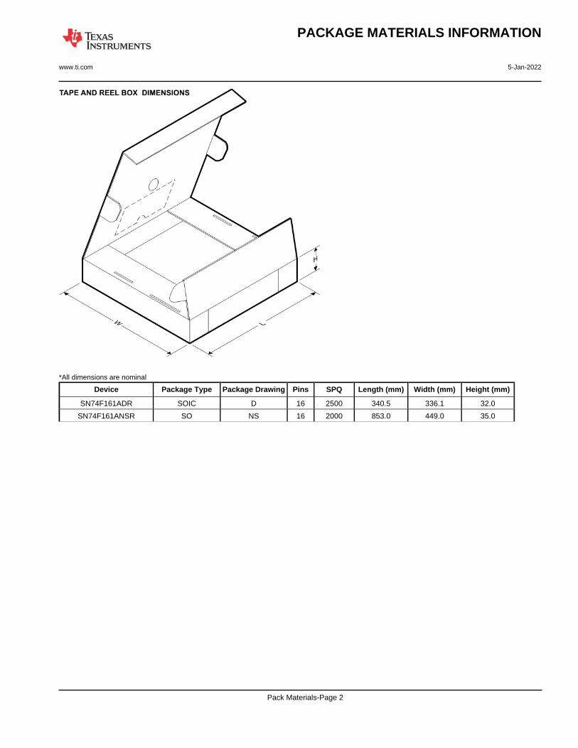
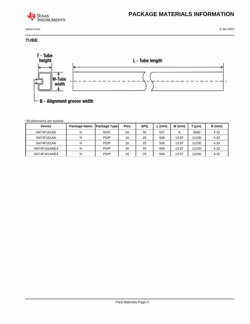
Device Package Name Package Type Pins SPQ L (mm) W (mm) T (µm) B (mm)
SN74F161AD D SOIC 16 40 507 8 3940 4.32
SN74F161AN N PDIP 16 25 506 13.97 11230 4.32
SN74F161AN N PDIP 16 25 506 13.97 11230 4.32
SN74F161ANE4 N PDIP 16 25 506 13.97 11230 4.32
SN74F161ANE4 N PDIP 16 25 506 13.97 11230 4.32
PACKAGE MATERIALS INFORMATION
www.ti.com 5-Jan-2022
Pack Materials-Page 3
IMPORTANT NOTICE AND DISCLAIMERTI PROVIDES TECHNICAL AND RELIABILITY DATA (INCLUDING DATA SHEETS), DESIGN RESOURCES (INCLUDING REFERENCE DESIGNS), APPLICATION OR OTHER DESIGN ADVICE, WEB TOOLS, SAFETY INFORMATION, AND OTHER RESOURCES “AS IS” AND WITH ALL FAULTS, AND DISCLAIMS ALL WARRANTIES, EXPRESS AND IMPLIED, INCLUDING WITHOUT LIMITATION ANY IMPLIED WARRANTIES OF MERCHANTABILITY, FITNESS FOR A PARTICULAR PURPOSE OR NON-INFRINGEMENT OF THIRD PARTY INTELLECTUAL PROPERTY RIGHTS.These resources are intended for skilled developers designing with TI products. You are solely responsible for (1) selecting the appropriate TI products for your application, (2) designing, validating and testing your application, and (3) ensuring your application meets applicable standards, and any other safety, security, regulatory or other requirements.These resources are subject to change without notice. TI grants you permission to use these resources only for development of an application that uses the TI products described in the resource. Other reproduction and display of these resources is prohibited. No license is granted to any other TI intellectual property right or to any third party intellectual property right. TI disclaims responsibility for, and you will fully indemnify TI and its representatives against, any claims, damages, costs, losses, and liabilities arising out of your use of these resources.TI’s products are provided subject to TI’s Terms of Sale or other applicable terms available either on ti.com or provided in conjunction with such TI products. TI’s provision of these resources does not expand or otherwise alter TI’s applicable warranties or warranty disclaimers for TI products.TI objects to and rejects any additional or different terms you may have proposed. IMPORTANT NOTICE