An IMPORTANT NOTICE at the end of this data sheet addresses availability, warranty, changes, use in safety-critical applications,intellectual property matters and other important disclaimers. PRODUCTION DATA.
SN74HC4066SCLS325H –MARCH 1996–REVISED AUGUST 2016
SN74HC4066 Quadruple Bilateral Analog Switch
1
1 Features1• Wide Operating Voltage Range of 2 V to 6 V• Typical Switch Enable Time of 18 ns• Low Power Consumption, 20-µA Maximum ICC
• Low Input Current of 1 µA Maximum• High Degree of Linearity• High On-Off Output-Voltage Ratio• Low Crosstalk Between Switches• Low On-State Impedance: 50-Ω Typical at
VCC = 6 V• Individual Switch Controls
2 Applications• Analog Signal Switching/Multiplexing:
– Signal Gating, Modulator, Squelch Control,Demodulator, Chopper, Commutating Switch
• Digital Signal Switching/Multiplexing– Audio and Video Signal Routing
• Transmission-Gate Logic Implementation• Analog-to-Digital and Digital-to-Analog Conversion• Digital Control of Frequency, Impedance, Phase,
and Analog-Signal Gain• Motor Speed Control• Battery Chargers• DC-DC Converter
3 DescriptionThe SN74HC4066 device is a silicon-gate CMOSquadruple analog switch designed to handle bothanalog and digital signals. Each switch permitssignals with amplitudes of up to 6 V (peak) to betransmitted in either direction.
Each switch section has its own enable input control(C). A high-level voltage applied to C turns on theassociated switch section.
Applications include signal gating, chopping,modulation or demodulation (modem), and signalmultiplexing for analog-to-digital and digital-to-analogconversion systems.
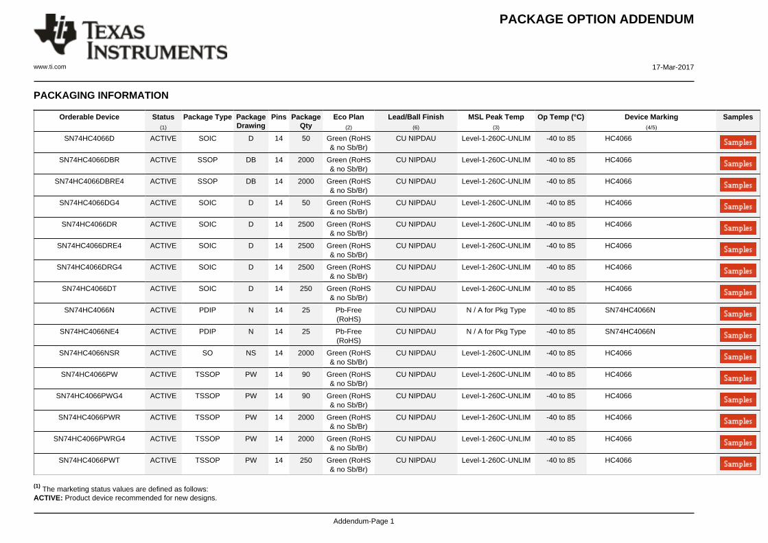
Device Information(1)
PART NUMBER PACKAGE(PINS) BODY SIZE (NOM)
SN74HC4066D SOIC (14) 8.65 mm × 3.91 mmSN74HC4066DB SSOP (14) 6.20 mm × 5.30 mmSN74HC4066PW TSSOP (14) 5..00 mm × 4.40 mmSN74HC4066N PDIP (14) 19.30 mm × 6.35 mmSN74HC4066NS SO (14) 10.30 mm × 5.30 mm
(1) For all available packages, see the orderable addendum atthe end of the data sheet.
10 Power Supply Recommendations ..................... 1511 Layout................................................................... 15
11.1 Layout Guidelines ................................................. 1511.2 Layout Example .................................................... 15
12 Device and Documentation Support ................. 1612.1 Documentation Support ........................................ 1612.2 Receiving Notification of Documentation Updates 1612.3 Community Resource............................................ 1612.4 Trademarks ........................................................... 1612.5 Electrostatic Discharge Caution............................ 1612.6 Glossary ................................................................ 16
13 Mechanical, Packaging, and OrderableInformation ........................................................... 16
4 Revision HistoryNOTE: Page numbers for previous revisions may differ from page numbers in the current version.
Changes from Revision G (July 2003) to Revision H Page
• Added ESD Ratings table, Feature Description section, Device Functional Modes, Application and Implementationsection, Power Supply Recommendations section, Layout section, Device and Documentation Support section, andMechanical, Packaging, and Orderable Information section ................................................................................................. 1
• Deleted Ordering Information table, see POA at the end of the datasheet............................................................................ 1
(1) Stresses beyond those listed under Absolute Maximum Ratings may cause permanent damage to the device. These are stress ratingsonly, which do not imply functional operation of the device at these or any other conditions beyond those indicated under RecommendedOperating Conditions. Exposure to absolute-maximum-rated conditions for extended periods may affect device reliability.
(2) All voltages are with respect to ground unless otherwise specified.
6 Specifications
6.1 Absolute Maximum Ratingsover operating free-air temperature range (unless otherwise noted) (1)
MIN MAX UNITVCC Supply voltage (2) –0.5 7 VII Control-input diode current VI < 0 or VI > VCC ±20 mAII I/O port diode current VI < 0 or VI/O > VCC ±20 mA
On-state switch current VI/O = 0 to VCC ±25 mAContinuous current through VCC or GND ±50 mA
TJ Junction temperature 150 °CTstg Storage temperature –60 150 °C
(1) JEDEC document JEP155 states that 500-V HBM allows safe manufacturing with a standard ESD control process.(2) JEDEC document JEP157 states that 250-V CDM allows safe manufacturing with a standard ESD control process. CDM value for N
package only.
6.2 ESD RatingsVALUE UNIT
V(ESD) Electrostatic dischargeHuman-body model (HBM), per ANSI/ESDA/JEDEC JS-001 (1) ±1000
VCharged-device model (CDM), per JEDEC specification JESD22-C101 (2) ±1000
(1) All unused inputs of the device must be held at VCC or GND to ensure proper device operation. See the TI applicationreport,Implications of Slow or Floating CMOS Inputs (SCBA004).
(2) With supply voltages at or near 2 V, the analog switch on-state resistance becomes very nonlinear. It is recommended that only digitalsignals be transmitted at these low supply voltages.
6.3 Recommended Operating Conditionsover operating free-air temperature range (unless otherwise noted) (1)
MIN NOM MAX UNITVCC Supply voltage 2 (2) 5 6 VVI/O I/O port voltage 0 VCC V
VIH High-level input voltage, control inputsVCC = 2 V 1.5 VCC
VVCC = 4.5 V 3.15 VCC
VCC = 6 V 4.2 VCC
VIL Low-level input voltage, control inputsVCC = 2 V 0 0.3
VVCC = 4.5 V 0 0.9VCC = 6 V 0 1.2
∆t/∆v Input transition rise and fall timeVCC = 2 V 1000
nsVCC = 4.5 V 500VCC = 6 V 400
TA Operating free-air temperature –40 85 °C
(1) For more information about traditional and new thermal metrics, see the Semiconductor and IC Package Thermal Metrics applicationreport.
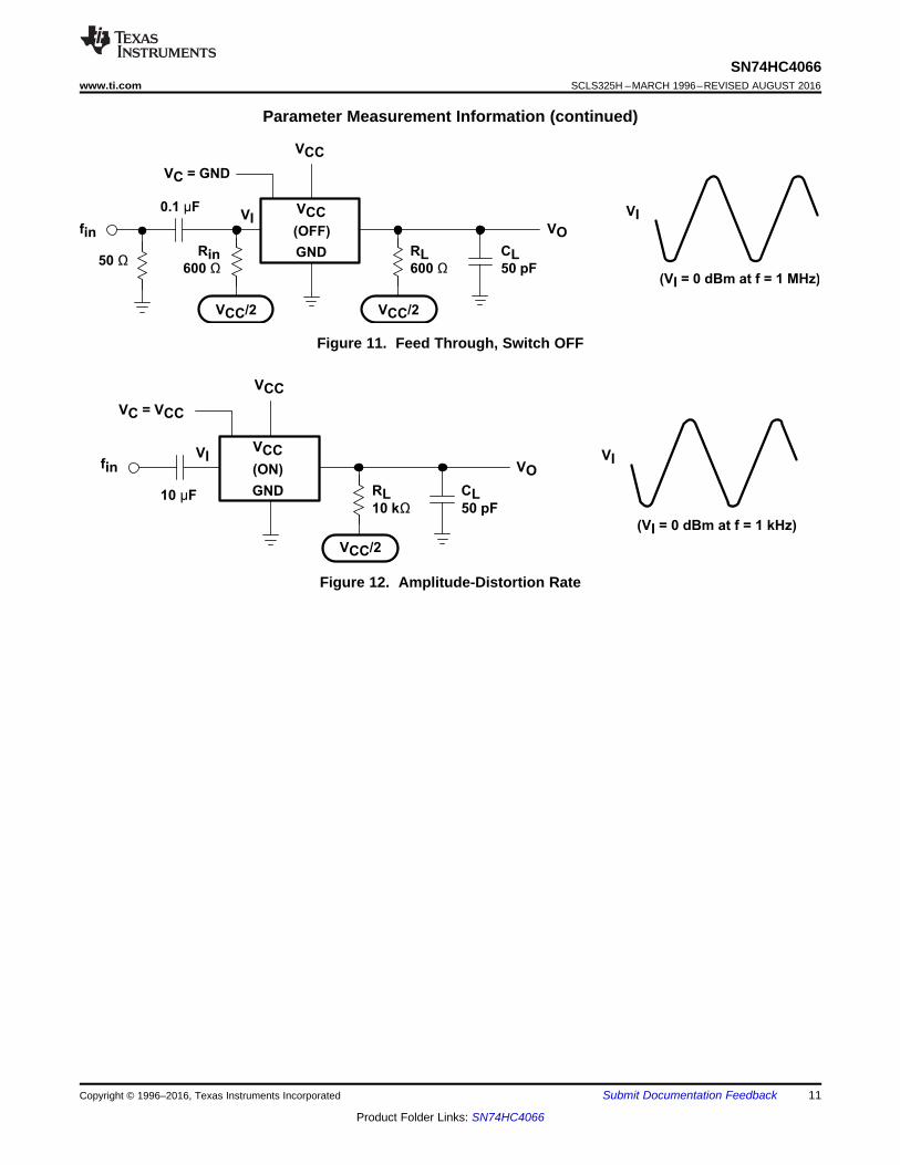
(1) Adjust the input amplitude for output = 0 dBm at f = 1 MHz. Input signal must be a sine wave.(2) Adjust the input amplitude for input = 0 dBm at f = 1 MHz. Input signal must be a sine wave.
6.7 Operating CharacteristicsVCC = 4.5 V, TA = 25°C
PARAMETER TEST CONDITIONS TYP UNITCpd Power dissipation capacitance per gate CL = 50 pF, f = 1 MHz 45 pF
Minimum through bandwidth, A to B or B to A (1) [20 log (VO / VI)] = –3 dB CL = 50 pF,VC = VCC
RL = 600 Ω,(see Figure 9) 30 MHz
Crosstalk between any switches (2) CL = 10 pF,fin = 1 MHz
RL = 50 Ω,(see Figure 10) 45 dB
Feed through, switch off, A to B or B to A (2) CL = 50 pF,fin = 1 MHz
RL = 600 Ω,(see Figure 11) 42 dB
Amplitude distortion rate, A to B or B to A CL = 50 pF,fin = 1 kHz
8.1 OverviewThe SN74HC4066 device is a silicon-gate CMOS quadruple analog switch designed for 2-V to 6-V VCCoperation. It is designed to handle both analog and digital signals. Each switch permits signals with amplitudes ofup to 6 V (peak) to be transmitted in either direction. A high-level voltage applied to the control pin C enables therespective switch to begin propagating signals across the device.
8.2 Functional Block Diagram
Figure 13. Logic Diagram, Each Switch(Positive Logic)
8.3 Feature DescriptionEach switch section has its own enable-input control (C). A high-level voltage applied to C turns on theassociated switch section, with typically 18 ns of switch enable time. The SN74HC4066 has a wide operatingvoltage range of 2 V to 6 V. It has low power consumption, with 20-µA maximum ICC and a low on-stateimpedance of 50 Ω. It also has low crosstalk between switches to minimize noise.
8.4 Device Functional ModesTable 1 lists the functions for the SN74HC4066 device.
NOTEInformation in the following applications sections is not part of the TI componentspecification, and TI does not warrant its accuracy or completeness. TI’s customers areresponsible for determining suitability of components for their purposes. Customers shouldvalidate and test their design implementation to confirm system functionality.
9.1 Application InformationThe SN74HC4066 can be used in any situation where an dual SPST switch would be used and a solid-state,voltage controlled version is preferred.
9.2 Typical Application
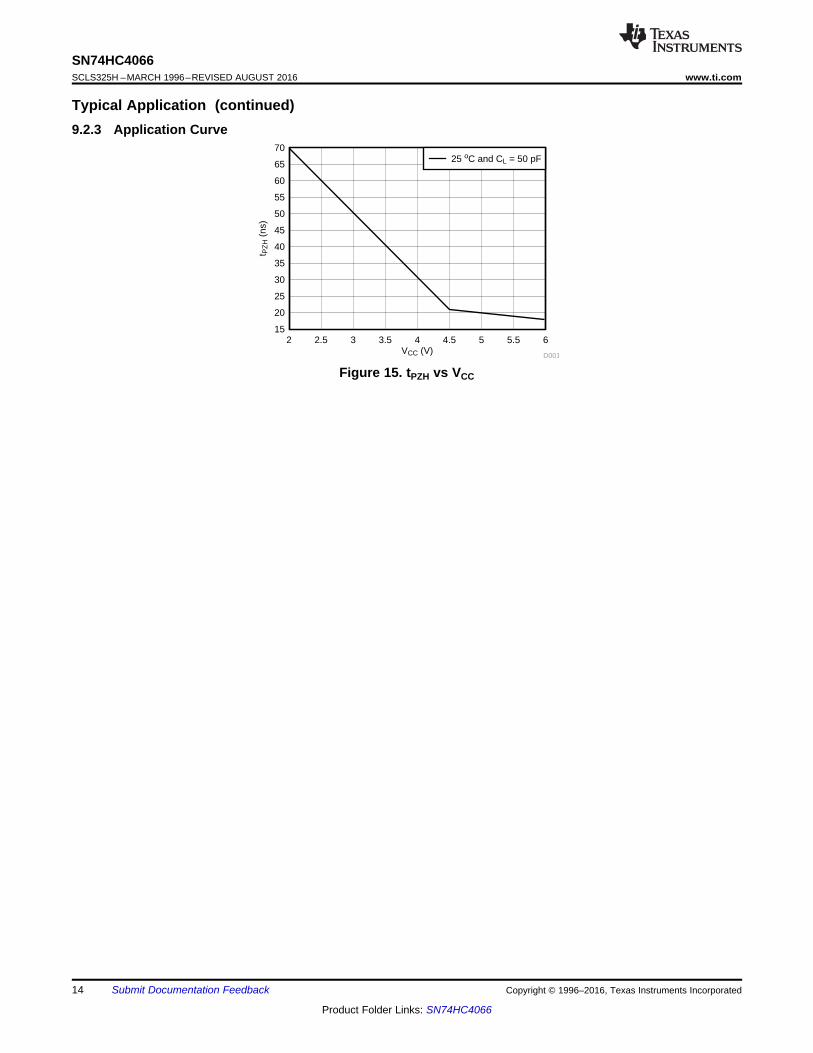
Figure 14. tPZH vs VCC
9.2.1 Design RequirementsThe SN74HC4066 allows ON/OFF control of analog and digital signals with a digital control signal. All inputsignals should remain between 0 V and VCC for optimal operation.
– For rise time and fall time specifications, see Δt/Δv in Recommended Operating Conditions.– For specified high and low levels, see VIH and VIL in Recommended Operating Conditions.
2. Recommended Output Conditions:– On-state switch current should not exceed ±25 mA.
10 Power Supply RecommendationsThe power supply can be any voltage between the minimum and maximum supply voltage rating located in theRecommended Operating Conditions.
Each VCC terminal should have a good bypass capacitor to prevent power disturbance. For devices with a singlesupply, TI recommends a 0.1-µF bypass capacitor. If there are multiple pins labeled VCC, then a 0.01-µF or0.022-µF capacitor is recommended for each VCC because the VCC pins will be tied together internally. Fordevices with dual-supply pins operating at different voltages, for example VCC and VDD, TI recommends a 0.1-µFbypass capacitor for each supply pin. It is acceptable to parallel multiple bypass capacitors to reject differentfrequencies of noise. 0.1-µF and 1-µF capacitors are commonly used in parallel. The bypass capacitor should beinstalled as close to the power terminal as possible for best results.
11 Layout
11.1 Layout GuidelinesReflections and matching are closely related to loop antenna theory, but different enough to warrant their owndiscussion. When a PCB trace turns a corner at a 90° angle, a reflection can occur. This is primarily due to thechange of width of the trace. At the apex of the turn, the trace width is increased to 1.414 times its width. Thisupsets the transmission line characteristics, especially the distributed capacitance and self-inductance of thetrace — resulting in the reflection.
NOTENot all PCB traces can be straight, and so they will have to turn corners. Figure 16 showsprogressively better techniques of rounding corners. Only the last example maintainsconstant trace width and minimizes reflections.
12.1.1 Related DocumentationFor related documentation see the following:
Implications of Slow or Floating CMOS Inputs (SCBA004)
12.2 Receiving Notification of Documentation UpdatesTo receive notification of documentation updates, navigate to the device product folder on ti.com. In the upperright corner, click on Alert me to register and receive a weekly digest of any product information that haschanged. For change details, review the revision history included in any revised document.
12.3 Community ResourceThe following links connect to TI community resources. Linked contents are provided "AS IS" by the respectivecontributors. They do not constitute TI specifications and do not necessarily reflect TI's views; see TI's Terms ofUse.
TI E2E™ Online Community TI's Engineer-to-Engineer (E2E) Community. Created to foster collaborationamong engineers. At e2e.ti.com, you can ask questions, share knowledge, explore ideas and helpsolve problems with fellow engineers.
Design Support TI's Design Support Quickly find helpful E2E forums along with design support tools andcontact information for technical support.
12.4 TrademarksE2E is a trademark of Texas Instruments.All other trademarks are the property of their respective owners.
12.5 Electrostatic Discharge CautionThese devices have limited built-in ESD protection. The leads should be shorted together or the device placed in conductive foamduring storage or handling to prevent electrostatic damage to the MOS gates.
12.6 GlossarySLYZ022 — TI Glossary.
This glossary lists and explains terms, acronyms, and definitions.
13 Mechanical, Packaging, and Orderable InformationThe following pages include mechanical, packaging, and orderable information. This information is the mostcurrent data available for the designated devices. This data is subject to change without notice and revision ofthis document. For browser-based versions of this data sheet, refer to the left-hand navigation.
LIFEBUY: TI has announced that the device will be discontinued, and a lifetime-buy period is in effect.NRND: Not recommended for new designs. Device is in production to support existing customers, but TI does not recommend using this part in a new design.PREVIEW: Device has been announced but is not in production. Samples may or may not be available.OBSOLETE: TI has discontinued the production of the device.
(2) Eco Plan - The planned eco-friendly classification: Pb-Free (RoHS), Pb-Free (RoHS Exempt), or Green (RoHS & no Sb/Br) - please check http://www.ti.com/productcontent for the latest availabilityinformation and additional product content details.TBD: The Pb-Free/Green conversion plan has not been defined.Pb-Free (RoHS): TI's terms "Lead-Free" or "Pb-Free" mean semiconductor products that are compatible with the current RoHS requirements for all 6 substances, including the requirement thatlead not exceed 0.1% by weight in homogeneous materials. Where designed to be soldered at high temperatures, TI Pb-Free products are suitable for use in specified lead-free processes.Pb-Free (RoHS Exempt): This component has a RoHS exemption for either 1) lead-based flip-chip solder bumps used between the die and package, or 2) lead-based die adhesive used betweenthe die and leadframe. The component is otherwise considered Pb-Free (RoHS compatible) as defined above.Green (RoHS & no Sb/Br): TI defines "Green" to mean Pb-Free (RoHS compatible), and free of Bromine (Br) and Antimony (Sb) based flame retardants (Br or Sb do not exceed 0.1% by weightin homogeneous material)
(3) MSL, Peak Temp. - The Moisture Sensitivity Level rating according to the JEDEC industry standard classifications, and peak solder temperature.
(4) There may be additional marking, which relates to the logo, the lot trace code information, or the environmental category on the device.
(5) Multiple Device Markings will be inside parentheses. Only one Device Marking contained in parentheses and separated by a "~" will appear on a device. If a line is indented then it is a continuationof the previous line and the two combined represent the entire Device Marking for that device.
(6) Lead/Ball Finish - Orderable Devices may have multiple material finish options. Finish options are separated by a vertical ruled line. Lead/Ball Finish values may wrap to two lines if the finishvalue exceeds the maximum column width.
Important Information and Disclaimer:The information provided on this page represents TI's knowledge and belief as of the date that it is provided. TI bases its knowledge and belief on informationprovided by third parties, and makes no representation or warranty as to the accuracy of such information. Efforts are underway to better integrate information from third parties. TI has taken andcontinues to take reasonable steps to provide representative and accurate information but may not have conducted destructive testing or chemical analysis on incoming materials and chemicals.TI and TI suppliers consider certain information to be proprietary, and thus CAS numbers and other limited information may not be available for release.
In no event shall TI's liability arising out of such information exceed the total purchase price of the TI part(s) at issue in this document sold by TI to Customer on an annual basis.
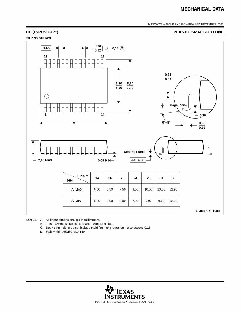
NOTES: A. All linear dimensions are in millimeters.B. This drawing is subject to change without notice.C. Body dimensions do not include mold flash or protrusion not to exceed 0,15.D. Falls within JEDEC MO-150
IMPORTANT NOTICE
Texas Instruments Incorporated (TI) reserves the right to make corrections, enhancements, improvements and other changes to itssemiconductor products and services per JESD46, latest issue, and to discontinue any product or service per JESD48, latest issue. Buyersshould obtain the latest relevant information before placing orders and should verify that such information is current and complete.TI’s published terms of sale for semiconductor products (http://www.ti.com/sc/docs/stdterms.htm) apply to the sale of packaged integratedcircuit products that TI has qualified and released to market. Additional terms may apply to the use or sale of other types of TI products andservices.Reproduction of significant portions of TI information in TI data sheets is permissible only if reproduction is without alteration and isaccompanied by all associated warranties, conditions, limitations, and notices. TI is not responsible or liable for such reproduceddocumentation. Information of third parties may be subject to additional restrictions. Resale of TI products or services with statementsdifferent from or beyond the parameters stated by TI for that product or service voids all express and any implied warranties for theassociated TI product or service and is an unfair and deceptive business practice. TI is not responsible or liable for any such statements.Buyers and others who are developing systems that incorporate TI products (collectively, “Designers”) understand and agree that Designersremain responsible for using their independent analysis, evaluation and judgment in designing their applications and that Designers havefull and exclusive responsibility to assure the safety of Designers' applications and compliance of their applications (and of all TI productsused in or for Designers’ applications) with all applicable regulations, laws and other applicable requirements. Designer represents that, withrespect to their applications, Designer has all the necessary expertise to create and implement safeguards that (1) anticipate dangerousconsequences of failures, (2) monitor failures and their consequences, and (3) lessen the likelihood of failures that might cause harm andtake appropriate actions. Designer agrees that prior to using or distributing any applications that include TI products, Designer willthoroughly test such applications and the functionality of such TI products as used in such applications.TI’s provision of technical, application or other design advice, quality characterization, reliability data or other services or information,including, but not limited to, reference designs and materials relating to evaluation modules, (collectively, “TI Resources”) are intended toassist designers who are developing applications that incorporate TI products; by downloading, accessing or using TI Resources in anyway, Designer (individually or, if Designer is acting on behalf of a company, Designer’s company) agrees to use any particular TI Resourcesolely for this purpose and subject to the terms of this Notice.TI’s provision of TI Resources does not expand or otherwise alter TI’s applicable published warranties or warranty disclaimers for TIproducts, and no additional obligations or liabilities arise from TI providing such TI Resources. TI reserves the right to make corrections,enhancements, improvements and other changes to its TI Resources. TI has not conducted any testing other than that specificallydescribed in the published documentation for a particular TI Resource.Designer is authorized to use, copy and modify any individual TI Resource only in connection with the development of applications thatinclude the TI product(s) identified in such TI Resource. NO OTHER LICENSE, EXPRESS OR IMPLIED, BY ESTOPPEL OR OTHERWISETO ANY OTHER TI INTELLECTUAL PROPERTY RIGHT, AND NO LICENSE TO ANY TECHNOLOGY OR INTELLECTUAL PROPERTYRIGHT OF TI OR ANY THIRD PARTY IS GRANTED HEREIN, including but not limited to any patent right, copyright, mask work right, orother intellectual property right relating to any combination, machine, or process in which TI products or services are used. Informationregarding or referencing third-party products or services does not constitute a license to use such products or services, or a warranty orendorsement thereof. Use of TI Resources may require a license from a third party under the patents or other intellectual property of thethird party, or a license from TI under the patents or other intellectual property of TI.TI RESOURCES ARE PROVIDED “AS IS” AND WITH ALL FAULTS. TI DISCLAIMS ALL OTHER WARRANTIES ORREPRESENTATIONS, EXPRESS OR IMPLIED, REGARDING RESOURCES OR USE THEREOF, INCLUDING BUT NOT LIMITED TOACCURACY OR COMPLETENESS, TITLE, ANY EPIDEMIC FAILURE WARRANTY AND ANY IMPLIED WARRANTIES OFMERCHANTABILITY, FITNESS FOR A PARTICULAR PURPOSE, AND NON-INFRINGEMENT OF ANY THIRD PARTY INTELLECTUALPROPERTY RIGHTS. TI SHALL NOT BE LIABLE FOR AND SHALL NOT DEFEND OR INDEMNIFY DESIGNER AGAINST ANY CLAIM,INCLUDING BUT NOT LIMITED TO ANY INFRINGEMENT CLAIM THAT RELATES TO OR IS BASED ON ANY COMBINATION OFPRODUCTS EVEN IF DESCRIBED IN TI RESOURCES OR OTHERWISE. IN NO EVENT SHALL TI BE LIABLE FOR ANY ACTUAL,DIRECT, SPECIAL, COLLATERAL, INDIRECT, PUNITIVE, INCIDENTAL, CONSEQUENTIAL OR EXEMPLARY DAMAGES INCONNECTION WITH OR ARISING OUT OF TI RESOURCES OR USE THEREOF, AND REGARDLESS OF WHETHER TI HAS BEENADVISED OF THE POSSIBILITY OF SUCH DAMAGES.Unless TI has explicitly designated an individual product as meeting the requirements of a particular industry standard (e.g., ISO/TS 16949and ISO 26262), TI is not responsible for any failure to meet such industry standard requirements.Where TI specifically promotes products as facilitating functional safety or as compliant with industry functional safety standards, suchproducts are intended to help enable customers to design and create their own applications that meet applicable functional safety standardsand requirements. Using products in an application does not by itself establish any safety features in the application. Designers mustensure compliance with safety-related requirements and standards applicable to their applications. Designer may not use any TI products inlife-critical medical equipment unless authorized officers of the parties have executed a special contract specifically governing such use.Life-critical medical equipment is medical equipment where failure of such equipment would cause serious bodily injury or death (e.g., lifesupport, pacemakers, defibrillators, heart pumps, neurostimulators, and implantables). Such equipment includes, without limitation, allmedical devices identified by the U.S. Food and Drug Administration as Class III devices and equivalent classifications outside the U.S.TI may expressly designate certain products as completing a particular qualification (e.g., Q100, Military Grade, or Enhanced Product).Designers agree that it has the necessary expertise to select the product with the appropriate qualification designation for their applicationsand that proper product selection is at Designers’ own risk. Designers are solely responsible for compliance with all legal and regulatoryrequirements in connection with such selection.Designer will fully indemnify TI and its representatives against any damages, costs, losses, and/or liabilities arising out of Designer’s non-compliance with the terms and provisions of this Notice.