Product Folder Sample & Buy Technical Documents Tools & Software Support & Community DP83848C, DP83848I DP83848VYB, DP83848YB SNLS266E – MAY 2007 – REVISED MARCH 2015 DP83848C/I/VYB/YB PHYTER™ QFP Single Port 10/100 Mb/s Ethernet Physical Layer Transceiver 1 Introduction 1.1 Features 1 • Multiple Temperature Range from –40°C to 105°C • IEEE 802.3 ENDEC, 10BASE-T Transceivers and Filters • Low-Power 3.3-V, 0.18-μm CMOS Technology • IEEE 802.3 PCS, 100BASE-TX Transceivers and • Low-Power Consumption < 270 mW Typical Filters • 3.3-V MAC Interface • IEEE 1149.1 JTAG • Auto-MDIX for 10/100 Mb/s • Integrated ANSI X3.263 Compliant TP-PMD • Energy Detection Mode Physical Sub-Layer with Adaptive Equalization and • 25-MHz Clock Output Baseline Wander Compensation • SNI Interface (Configurable) • Error-Free Operation up to 150 Meters • RMII Rev. 1.2 Interface (Configurable) • Programmable LED Support for Link, 10/100 Mb/s • MII Serial Management Interface (MDC and MDIO) Mode, Activity, Duplex and Collision Detect • IEEE 802.3 MII • Single Register Access for Complete PHY Status • IEEE 802.3 Auto-Negotiation and Parallel • 10/100 Mb/s Packet BIST (Built in Self Test) Detection 1.2 Applications • Automotive/Transportation • General Embedded Applications • Industrial Controls and Factory Automation 1.3 Description The number of applications requiring Ethernet connectivity continues to increase, driving Ethernet enabled devices into harsher environments. The DP83848C/I/VYB/YB was designed to meet the challenge of these new applications with an extended temperature performance that goes beyond the typical Industrial temperature range. The DP83848C/I/VYB/YB is a highly reliable, feature rich, robust device which meets IEEE 802.3 standards over multiple temperature ranges from commercial to extreme temperatures. This device is ideally suited for harsh environments such as wireless remote base stations, automotive/transportation, and industrial control applications. It offers enhanced ESD protection and the choice of an MII or RMII interface for maximum flexibility in MPU selection; all in a 48 pin package. The DP83848VYB extends the leadership position of the PHYTER™ family of devices with a wide operating temperature range. The TI line of PHYTER transceivers builds on decades of Ethernet expertise to offer the high performance and flexibility that allows the end user an easy implementation tailored to meet these application needs. Device Information (1) PART NUMBER PACKAGE BODY SIZE (NOM) DP83848VYB/YB HLQFP (48) 7.00 mm × 7.00 mm DP83848I/C LQFP (48) (1) For more information, see Section 9, Mechanical, Packaging, and Orderable Information. 1 An IMPORTANT NOTICE at the end of this data sheet addresses availability, warranty, changes, use in safety-critical applications, intellectual property matters and other important disclaimers. PRODUCTION DATA.
Transcript
Product
Folder
Sample &Buy
Technical
Documents
Tools &
Software
Support &Community
DP83848C, DP83848IDP83848VYB, DP83848YB
SNLS266E –MAY 2007–REVISED MARCH 2015
DP83848C/I/VYB/YB PHYTER™ QFP Single Port 10/100 Mb/s EthernetPhysical Layer Transceiver
1 Introduction
1.1 Features1
• Multiple Temperature Range from –40°C to 105°C • IEEE 802.3 ENDEC, 10BASE-T Transceivers andFilters• Low-Power 3.3-V, 0.18-µm CMOS Technology
• IEEE 1149.1 JTAG• Auto-MDIX for 10/100 Mb/s• Integrated ANSI X3.263 Compliant TP-PMD• Energy Detection Mode
Physical Sub-Layer with Adaptive Equalization and• 25-MHz Clock Output Baseline Wander Compensation• SNI Interface (Configurable) • Error-Free Operation up to 150 Meters• RMII Rev. 1.2 Interface (Configurable) • Programmable LED Support for Link, 10/100 Mb/s• MII Serial Management Interface (MDC and MDIO) Mode, Activity, Duplex and Collision Detect• IEEE 802.3 MII • Single Register Access for Complete PHY Status• IEEE 802.3 Auto-Negotiation and Parallel • 10/100 Mb/s Packet BIST (Built in Self Test)
Detection
1.2 Applications• Automotive/Transportation • General Embedded Applications• Industrial Controls and Factory Automation
1.3 DescriptionThe number of applications requiring Ethernet connectivity continues to increase, driving Ethernet enableddevices into harsher environments.
The DP83848C/I/VYB/YB was designed to meet the challenge of these new applications with an extendedtemperature performance that goes beyond the typical Industrial temperature range. TheDP83848C/I/VYB/YB is a highly reliable, feature rich, robust device which meets IEEE 802.3 standardsover multiple temperature ranges from commercial to extreme temperatures. This device is ideally suitedfor harsh environments such as wireless remote base stations, automotive/transportation, and industrialcontrol applications.
It offers enhanced ESD protection and the choice of an MII or RMII interface for maximum flexibility inMPU selection; all in a 48 pin package.
The DP83848VYB extends the leadership position of the PHYTER™ family of devices with a wideoperating temperature range. The TI line of PHYTER transceivers builds on decades of Ethernet expertiseto offer the high performance and flexibility that allows the end user an easy implementation tailored tomeet these application needs.
Device Information (1)
PART NUMBER PACKAGE BODY SIZE (NOM)DP83848VYB/YB HLQFP (48)
7.00 mm × 7.00 mmDP83848I/C LQFP (48)
(1) For more information, see Section 9, Mechanical, Packaging, and Orderable Information.
1
An IMPORTANT NOTICE at the end of this data sheet addresses availability, warranty, changes, use in safety-critical applications,intellectual property matters and other important disclaimers. PRODUCTION DATA.
The DP83848VYB pins are classified into the following interface categories (each interface is described inthe sections that follow):• Serial Management Interface• MAC Data Interface• Clock Interface• LED Interface• JTAG Interface• Reset and Power Down• Strap Options• 10/100 Mb/s PMD Interface• Special Connect Pins• Power and Ground pins
NOTEStrapping pin option. See Section 4.9 for strap definitions.
All DP83848VYB signal pins are I/O cells regardless of the particular use. The definitions below define thefunctionality of the I/O cells for each pin.
Type: I Input
Type: O Output
Type: I/O Input/Output
Type: OD Open Drain
Type: PD,PU Internal Pulldown/Pullup
Type: S Strapping Pin (All strap pins have weak internal pullups or pulldowns. If the default strapvalue is to be changed then an external 2.2 kΩ resistor should be used. See Section 4.9 fordetails.)
4.3 Serial Management InterfaceSIGNAL TYPE PIN # DESCRIPTIONNAME
MDC I 31 MANAGEMENT DATA CLOCK: Synchronous clock to the MDIO management data input/outputserial interface which may be asynchronous to transmit and receive clocks. The maximum clockrate is 25 MHz with no minimum clock rate.
MDIO I/O 30 MANAGEMENT DATA I/O: Bi-directional management instruction/data signal that may besourced by the station management entity or the PHY. This pin requires a 1.5 kΩ pullup resistor.
4.4 Mac Data InterfaceSIGNAL TYPE PIN # DESCRIPTIONNAME
TX_CLK O 1 MII TRANSMIT CLOCK: 25 MHz Transmit clock output in 100 Mb/s mode or 2.5 MHz in 10 Mb/smode derived from the 25 MHz reference clock.Unused in RMII mode. The device uses the X1 reference clock input as the 50 MHz reference forboth transmit and receive.SNI TRANSMIT CLOCK: 10 MHz Transmit clock output in 10 Mb SNI mode. The MAC shouldsource TX_EN and TXD_0 using this clock.
TX_EN I, PD 2 MII TRANSMIT ENABLE: Active high input indicates the presence of valid data inputs onTXD[3:0].RMII TRANSMIT ENABLE: Active high input indicates the presence of valid data on TXD[1:0].SNI TRANSMIT ENABLE: Active high input indicates the presence of valid data on TXD_0.
TXD_0 I 3 MII TRANSMIT DATA: Transmit data MII input pins, TXD[3:0], that accept data synchronous toTXD_1 4 the TX_CLK (2.5 MHz in 10 Mb/s mode or 25 MHz in 100 Mb/s mode).TXD_2 5 RMII TRANSMIT DATA: Transmit data RMII input pins, TXD[1:0], that accept data synchronous toTXD_3 S, I, PD 6 the 50 MHz reference clock.
SNI TRANSMIT DATA: Transmit data SNI input pin, TXD_0, that accept data synchronous to theTX_CLK (10 MHz in 10 Mb/s SNI mode).
RX_CLK O 38 MII RECEIVE CLOCK: Provides the 25 MHz recovered receive clocks for 100 Mb/s mode and 2.5MHz for 10 Mb/s mode.Unused in RMII mode. The device uses the X1 reference clock input as the 50 MHz reference forboth transmit and receive.SNI RECEIVE CLOCK: Provides the 10 MHz recovered receive clocks for 10 Mb/s SNI mode.
RX_DV S, O, PD 39 MII RECEIVE DATA VALID: Asserted high to indicate that valid data is present on thecorresponding RXD[3:0]. Mll mode by default with internal pulldown.RMII Synchronous RECEIVE DATA VALID:This signal provide the RMII Receive Data Validindication independent of Carrier Sense.This pin is not used in SNI mode.
RX_ER S, O, PU 41 MII RECEIVE ERROR: Asserted high synchronously to RX_CLK to indicate that an invalid symbolhas been detected within a received packet in 100 Mb/s mode.RMII RECEIVE ERROR: Asserted high synchronously to X1 whenever an invalid symbol isdetected, and CRS_DV is asserted in 100 Mb/s mode.This pin is not required to be used by a MAC in either MII or RMII mode, since the Phy is requiredto corrupt data on a receive error.This pin is not used in SNI mode.
RXD_0 S, O, PD 43 MII RECEIVE DATA: Nibble wide receive data signals driven synchronously to the RX_CLK, 25RXD_1 44 MHz for 100 Mb/s mode, 2.5 MHz for 10 Mb/s mode). RXD[3:0] signals contain valid data whenRXD_2 45 RX_DV is asserted.RXD_3 46 RMII RECEIVE DATA: 2-bits receive data signals, RXD[1:0], driven synchronously to the X1 clock,
50 MHz.SNI RECEIVE DATA: Receive data signal, RXD_0, driven synchronously to the RX_CLK. RXD_0contains valid data when CRS is asserted. RXD[3:1] are not used in this mode.
CRS/CRS_D S, O, PU 40 MII CARRIER SENSE: Asserted high to indicate the receive medium is non-idle.V RMII CARRIER SENSE/RECEIVE DATA VALID: This signal combines the RMII Carrier and
Receive Data Valid indications. For a detailed description of this signal, see the RMII Specification.SNI CARRIER SENSE: Asserted high to indicate the receive medium is non-idle. It is used toframe valid receive data on the RXD_0 signal.
COL S, O, PU 42 MII COLLISION DETECT: Asserted high to indicate detection of a collision condition(simultaneous transmit and receive activity) in 10 Mb/s and 100 Mb/s Half Duplex Modes.While in 10BASE-T Half Duplex mode with heartbeat enabled this pin is also asserted for aduration of approximately 1µs at the end of transmission to indicate heartbeat (SQE test).In Full Duplex Mode, for 10 Mb/s or 100 Mb/s operation, this signal is always logic 0. There is noheartbeat function during 10 Mb/s full duplex operation.RMII COLLISION DETECT: Per the RMII Specification, no COL signal is required. The MAC willrecover CRS from the CRS_DV signal and use that along with its TX_EN signal to determinecollision.SNI COLLISION DETECT: Asserted high to indicate detection of a collision condition(simultaneous transmit and receive activity) in 10 Mb/s SNI mode.
4.5 Clock InterfaceSIGNAL TYPE PIN # DESCRIPTIONNAME
X1 I 34 CRYSTAL/OSCILLATOR INPUT: This pin is the primary clock reference input for theDP83848C/I/VYB/YB and must be connected to a 25 MHz 0.005% (±50 ppm) clock source.The DP83848C/I/VYB/YB supports either an external crystal resonator connected across pinsX1 and X2, or an external CMOS-level oscillator source connected to pin X1 only.RMII REFERENCE CLOCK: This pin is the primary clock reference input for the RMII modeand must be connected to a 50 MHz 0.005% (±50 ppm) CMOS-level oscillator source.
X2 O 33 CRYSTAL OUTPUT: This pin is the primary clock reference output to connect to an external25 MHz crystal resonator device. This pin must be left unconnected if an external CMOSoscillator clock source is used.
CLK_OUT O 25 25 MHz CLOCK OUTPUT:In MII mode, this pin provides a 25 MHz clock output to the system.In RMII mode, this pin provides a 50 MHz clock output to the system.This allows other devices to use the reference clock from the DP83848VYB without requiringadditional clock sources.
DP83848C, DP83848IDP83848VYB, DP83848YBSNLS266E –MAY 2007–REVISED MARCH 2015 www.ti.com
4.6 LED InterfaceSee Table 6-2 for LED Mode Selection.
SIGNAL NAME TYPE PIN # DESCRIPTIONLED_LINK S, O, PU 28 LINK LED: In Mode 1, this pin indicates the status of the LINK. The LED will be
ON when Link is good.LINK/ACT LED: In Mode 2 and Mode 3, this pin indicates transmit and receiveactivity in addition to the status of the Link. The LED will be ON when Link isgood. It will blink when the transmitter or receiver is active.
LED_SPEED S, O, PU 27 SPEED LED: The LED is ON when device is in 100 Mb/s and OFF when in 10Mb/s. Functionality of this LED is independent of mode selected.
LED_ACT/COL S, O, PU 26 ACTIVITY LED: In Mode 1, this pin is the Activity LED which is ON when activityis present on either Transmit or Receive.COLLISION/DUPLEX LED: In Mode 2, this pin by default indicates Collisiondetection. For Mode 3, this LED output may be programmed to indicate Full-duplex status instead of Collision.
4.7 JTAG Interface for DP83848I/VYB/YBSIGNAL NAME TYPE PIN # (1) DESCRIPTION
TCK I, PU 8 TEST CLOCKThis pin has a weak internal pullup.
TDI I, PU 12 TEST DATA INPUTThis pin has a weak internal pullup.
TDO O 9 TEST OUTPUTTMS I, PU 10 TEST MODE SELECT
This pin has a weak internal pullup.TRST# I, PU 11 TEST RESET: Active low asynchronous test reset.
This pin has a weak internal pullup.
(1) DP83848C does not support JTAG. Pins 8-12 should be left unconnected.
4.8 Reset and Power DownSIGNAL NAME TYPE PIN # DESCRIPTION
RESET_N I, PU 29 RESET: Active Low input that initializes or re-initializes the DP83848VYB. Assertingthis pin low for at least 1 µs will force a reset process to occur. All internal registerswill re-initialize to their default states as specified for each bit in the Section 6.6section. All strap options are re-initialized as well.
PWR_DOWN/INT I, PU 7 See Section 7.2.1.3.1 for detailed description.The default function of this pin is POWER DOWN.POWER DOWN: The pin is an active low input in this mode and should beasserted low to put the device in a Power Down mode.INTERRUPT: The pin is an open drain output in this mode and will be asserted lowwhen an interrupt condition occurs. Although the pin has a weak internal pullup,some applications may require an external pullup resister. Register access isrequired for the pin to be used as an interrupt mechanism. See Section 7.2.1.3.1.2for more details on the interrupt mechanisms.
4.9 Strap OptionsThe DP83848VYB uses many of the functional pins as strap options. The values of these pins aresampled during reset and used to strap the device into specific modes of operation. The strap option pinassignments are defined below. The functional pin name is indicated in parentheses.
A 2.2 kΩ resistor should be used for pulldown or pullup to change the default strap option. If the defaultoption is required, then there is no need for external pullup or pulldown resistors. Since these pins mayhave alternate functions after reset is deasserted, they should not be connected directly to VCC or GND.
SIGNAL NAME TYPE PIN # DESCRIPTIONPHYAD0 (COL) S, O, PU 42 PHY ADDRESS [4:0]: The DP83848VYB provides five PHY address pins, the state ofPHYAD1 (RXD1_0) S, O, PD 43 which are latched into the PHYCTRL register at system Hardware-Reset.PHYAD2 (RXD0_1) 44 The DP83848VYB supports PHY Address strapping values 0 (<00000>) through 31PHYAD3 (RXD1_2) 45 (<11111>).A PHY Adress of 0 puts the part into the Mll isolate Mode. The Mll isolatePHYAD4 (RXD1_3) 46 mode must be selected by strapping Phy Address 0; changing to Address 0 by register
write will not put the Phy in the Mll isolate mode. Please refer to Section 6.4.5 foradditional information.PHYAD0 pin has weak internal pullup resistor.PHYAD[4:1] pins have weak internal pulldown resistors.
AN_EN(LED_ACT/COL) S, O, PU 26 Auto-Negotiation Enable: When high, this enables Auto-Negotiation with the capabilityAN_1 (LED_SPEED) 27 set by AN0 and AN1 pins. When low, this puts the part into Forced Mode with theAN_0 (LED_LINK) 28 capability set by AN0 and AN1 pins.
AN0 / AN1: These input pins control the forced or advertised operating mode of theDP83848VYB according to the following table. The value on these pins is set byconnecting the input pins to GND (0) or VCC (1) through 2.2 kΩ resistors. These pinsshould NEVER be connected directly to GND or VCC.The value set at this input is latched into the DP83848VYB at Hardware-Reset.The float/pulldown status of these pins are latched into the Basic Mode Control Registerand the Auto_Negotiation Advertisement Register during Hardware-Reset.The default is 111 since the these pin have internal pullups.
100BASE-TX, Half/Full-DuplexMII_MODE (RX_DV) S, O, PD 39 MII MODE SELECT: This strapping option pair determines the operating mode of theSNI_MODE (TXD_3) 6 MAC Data Interface. Default operation (No pullups) will enable normal MII Mode of
operation. Strapping MII_MODE high will cause the device to be in RMII or SNI modes ofoperation, determined by the status of the SNI_MODE strap. Since the pins includeinternal pulldowns, the default values are 0.The following table details the configurations:
MII_MODE SNI_MODE MAC Interface Mode0 X MII Mode1 0 RMII Mode1 1 10 Mb SNI Mode
LED_CFG (CRS) S, O, PU 40 LED CONFIGURATION: This strapping option determines the mode of operation of theLED pins. Default is Mode 1. Mode 1 and Mode 2 can be controlled through the strapoption. All modes are configurable through register access.See Table 6-2 for LED Mode Selection.
MDIX_EN (RX_ER) S, O, PU 41 MDIX ENABLE: Default is to enable MDIX. This strapping option disables Auto-MDIX. Anexternal pulldown will disable Auto-MDIX mode.
4.10 10 Mb/s and 100 Mb/s PMD InterfaceSIGNAL NAME TYPE PIN # DESCRIPTION
TD-, TD+ I/O 16 Differential common driver transmit output (PMD Output Pair). These differential outputs17 are automatically configured to either 10BASE-T or 100BASE-TX signaling.
IIn Auto-MDIX mode of operation, this pair can be used as the Receive Input pair.These pins require 3.3-V bias for operation.
DP83848C, DP83848IDP83848VYB, DP83848YBSNLS266E –MAY 2007–REVISED MARCH 2015 www.ti.com
SIGNAL NAME TYPE PIN # DESCRIPTIONRD-, RD+ I/O 13 Differential receive input (PMD Input Pair). These differential inputs are automatically
14 configured to accept either 100BASE-TX or 10BASE-T signaling.In Auto-MDIX mode of operation, this pair can be used as the Transmit Output pair.These pins require 3.3-V bias for operation.
4.11 Special ConnectionsSIGNAL NAME TYPE PIN # DESCRIPTION
RBIAS I 24 Bias Resistor Connection: A 4.87 kΩ 1% resistor should be connected from RBIAS toGND.
PFBOUT O 23 Power Feedback Output: Parallel caps, 10 µF (Tantalum preferred) and 0.1 µF, should beplaced close to the PFBOUT. Connect this pin to PFBIN1 (pin 18) and PFBIN2 (pin 37). SeeSection 7.2.1.3 for proper placement pin.
PFBIN1 I 18 Power Feedback Input: These pins are fed with power from PFBOUT pin. A small capacitorPFBIN2 37 of 0.1 µF should be connected close to each pin. (1)
RESERVED I/O 20, 21 RESERVED: These pins must be pulled-up through 2.2 kΩ resistors to AVDD33 supply.
(1) Note: Do not supply power to these pins other than from PFBOUT.
4.12 Power Supply PinsSIGNAL NAME PIN # DESCRIPTION
IOVDD33 32, 38 I/O 3.3-V SupplyIOGND 35, 47 I/O GroundDGND 36 Digital GroundAVDD33 22 Analog 3.3-V SupplyAGND 15, 19 Analog GroundGNDPAD 49 Ground PAD
MIN MAX UNITSupply Voltage (VCC) –0.5 4.2 VDC Input Voltage (VIN) –0.5 VCC + 0.5 VDC Output Voltage (VOUT) –0.5 VCC + 0.5 VMaximum Die Temperature 121.5 °CLead Temperature (TL) (Soldering, 10 sec.) 260 °CStorage Temperature, Tstg –65 150 °C
(1) Stresses beyond those listed under Absolute Maximum Ratings may cause permanent damage to the device. These are stress ratingsonly, which do not imply functional operation of the device at these or any other conditions beyond those indicated under RecommendedOperating Conditions. Exposure to absolute-maximum-rated conditions for extended periods may affect device reliability.
(2) If Military/Aerospace specified devices are required, please contact the TI Sales Office/ Distributors for availability and specifications.
5.2 ESD RatingsVALUE UNIT
Human body model (HBM), per ANSI/ESDA/JEDEC JS-001, all pins (1) ±4000V(ESD) Electrostatic discharge VCharged device model (CDM), per JEDEC specification JESD22-C101, all ±1000
pins (2)
(1) JEDEC document JEP155 states that 500-V HBM allows safe manufacturing with a standard ESD control process.(2) JEDEC document JEP157 states that 250-V CDM allows safe manufacturing with a standard ESD control process.
5.3 Recommended Operating ConditionsMIN MAX UNIT
Supply voltage (VCC) 3.3 V ± 0.3 VCommercial 0 70Industrial –40 85
5.6 AC Timing RequirementsPARAMETER DESCRIPTION NOTES MIN TYP MAX UNIT
POWER-UP TIMINGMDIO is pulled high for 32-bit serial
Post Power-Up Stabilization management initializationT2.1.1 time prior to MDC preamble for 167 ms
X1 Clock must be stable for a min.register accesses (1)of 167 ms at power up.Hardware Configuration Pins aredescribed in the Section 4 section.Hardware Configuration Latch-T2.1.2 167 msin Time from power up (1) X1 Clock must be stable for a min.of 167 ms at power up.
Hardware Configuration pinsT2.1.3 50 nstransition to output driversRESET TIMING
Post RESET Stabilization time MDIO is pulled high for 32-bit serialT2.2.1 prior to MDC preamble for 3 µsmanagement initializationregister accesses (2)
Hardware Configuration Latch- Hardware Configuration Pins areT2.2.2 in Time from the Deassertion of 3 µsdescribed in the Section 4 sectionRESET (either soft or hard) (2)
Hardware Configuration pinsT2.2.3 50 nstransition to output driversX1 Clock must be stable for at min.
T2.2.4 RESET pulse width of 1us during RESET pulse low 1 µstime.
MII SERIAL MANAGEMENT TIMINGMDC to MDIO (Output) DelayT2.3.1 0 30 nsTimeMDIO (Input) to MDC SetupT2.3.2 10 nsTimeMDIO (Input) to MDC HoldT2.3.3 10 nsTime
T2.3.4 MDC Frequency 2.5 25 MHz100 Mb/s MII TRANSMIT TIMINGT2.4.1 TX_CLK High/Low Time 100 Mb/s Normal mode 16 20 24 ns
TXD[3:0], TX_EN Data Setup toT2.4.2 100 Mb/s Normal mode 10 nsTX_CLKTXD[3:0], TX_EN Data HoldT2.4.3 100 Mb/s Normal mode 0 nsfrom TX_CLK
100 Mb/s MII RECEIVE TIMINGT2.5.1 RX_CLK High/Low Time (3) 100 Mb/s Normal mode 16 20 24 ns
RX_CLK to RXD[3:0], RX_DV,T2.5.2 100 Mb/s Normal mode 10 30 nsRX_ER Delay100BASE-TX MII TRANSMIT PACKET LATENCY TIMING
TX_CLK to PMD Output PairT2.6.1 100BASE-TX mode 6 bitsLatency (4)
(1) In RMII Mode, the minimum Post Power-up Stabilization and Hardware Configuration Latch-in times are 84ms.(2) It is important to choose pullup and/or pulldown resistors for each of the hardware configuration pins that provide fast RC time constants
in order to latch-in the proper value prior to the pin transitioning to an output driver.(3) RX_CLK may be held low or high for a longer period of time during transition between reference and recovered clocks. Minimum high
and low times will not be violated.(4) For Normal mode, latency is determined by measuring the time from the first rising edge of TX_CLK occurring after the assertion of
TX_EN to the first bit of the “J” code group as output from the PMD Output Pair. 1 bit time = 10 ns in 100 Mb/s mode.(5) Deassertion is determined by measuring the time from the first rising edge of TX_CLK occurring after the deassertion of TX_EN to the
first bit of the “T” code group as output from the PMD Output Pair. 1 bit time = 10 ns in 100 Mb/s mode.
T2.9.1 Carrier Sense ON Delay (9) 100 Mb/s Normal mode (10) 20 bitsT2.9.2 Receive Data Latency 100 Mb/s Normal mode (10) 24 bits100BASE-TX RECEIVE PACKET DEASSERTION TIMINGT2.10.1 Carrier Sense OFF Delay (11) 100 Mb/s Normal mode (10) 24 bits10 Mb/s MII TRANSMIT TIMING (12)
T2.11.1 TX_CLK High/Low Time 10 Mb/s MII mode 190 200 210 nsTXD[3:0], TX_EN Data Setup toT2.11.2 10 Mb/s MII mode 25 nsTX_CLK fallTXD[3:0], TX_EN Data HoldT2.11.3 10 Mb/s MII mode 0 nsfrom TX_CLK rise
10 Mb/s MII RECEIVE TIMINGT2.12.1 RX_CLK High/Low Time (13) 160 200 240 ns
RX_CLK TO RXD[3:0, RX_DVT2.12.2 10 Mb/s MII mode 100 nsDelayRX_CLK rising edge delay fromT2.12.3 10 Mb/s MII mode 100 nsRXD[3:0], RX_DV Valid
10 Mb/s SERIAL MODE (SNI) TRANSMIT TIMINGT2.13.1 TX_CLK High Time 10 Mb/s Serial mode (SNI) 20 25 30 nsT2.13.2 TX_CLK Low Time 10 Mb/s Serial mode (SNI) 70 75 80 ns
TXD_0, TX_EN Data Setup toT2.13.3 10 Mb/s Serial mode (SNI) 25 nsTX_CLK riseTXD_0, TX_EN Data Hold fromT2.13.4 10 Mb/s Serial mode (SNI) 0 nsTX_CLK rise
10 Mb/s SERIAL MODE (SNI) RECEIVE TIMINGT2.14.1 RX_CLK High/Low Time (14) 35 50 65 ns
RX_CLK fall to RXD_0, RX_DVT2.14.2 10 Mb/s Serial mode (SNI) –10 10 nsDelay10BASE-T TRANSMIT TIMING (START OF PACKET)
Transmit Output Delay from theT2.15.1 10 Mb/s MII mode (15) 3.5 bits
Falling Edge of TX_CLKTransmit Output Delay from the
T2.15.2 10 Mb/s Serial mode (SNI) (15) 3.5 bitsRising Edge of TX_CLK
(6) Rise and fall times taken at 10% and 90% of the +1 or -1 amplitude(7) Normal Mismatch is the difference between the maximum and minimum of all rise and fall times(8) PMD Input Pair voltage amplitude is greater than the Signal Detect Turnon Threshold Value.(9) Carrier Sense On Delay is determined by measuring the time from the first bit of the “J” code group to the assertion of Carrier Sense.(10) 1 bit time = 10 ns in 100 Mb/s mode.(11) Carrier Sense Off Delay is determined by measuring the time from the first bit of the “T” code group to the deassertion of Carrier Sense.(12) An attached Mac should drive the transmit signals using the positive edge of TX_CLK. As shown above, the MII signals are sampled on
the falling edge of TX_CLK.(13) RX_CLK may be held low for a longer period of time during transition between reference and recovered clocks. Minimum high and low
times will not be violated.(14) RX_CLK may be held high for a longer period of time during transition between reference and recovered clocks. Minimum high and low
times will not be violated.(15) 1 bit time = 100 ns in 10 Mb/s.
TXD[1:0], TX_EN, Data SetupT2.26.2 4 nsto X1 risingTXD[1:0], TX_EN, Data HoldT2.26.3 2 nsfrom X1 rising
(16) 1 bit time = 100 ns in 10 Mb/s mode.(17) 10BASE-T RX_DV Latency is measured from first bit of preamble on the wire to the assertion of RX_DV(18) These specifications represent transmit timings.(19) The signal amplitude on PMD Input Pair must be TP-PMD compliant.(20) Measurement is made from the first rising edge of TX_CLK after assertion of TX_EN.(21) Due to the nature of the descrambler function, all 100BASE-TX Loopback modes will cause an initial “dead-time” of up to 550 µs during
which time no data will be present at the receive MII outputs. The 100BASE-TX timing specified is based on device delays after theinitial 550µs “dead-time”.
DP83848C, DP83848IDP83848VYB, DP83848YBSNLS266E –MAY 2007–REVISED MARCH 2015 www.ti.com
AC Timing Requirements (continued)PARAMETER DESCRIPTION NOTES MIN TYP MAX UNIT
X1 Clock to PMD Output Pair From X1 Rising edge to first bit ofT2.26.4 17 bitsLatency symbolRMII RECEIVE TIMINGT2.27.1 X1 Clock Period 50 MHz Reference Clock 20 ns
RXD[1:0], CRS_DV, RX_DVT2.27.2 and RX_ER output delay from 2 14 ns
X1 rising (22) (23) (24)
From JK symbol on PMD ReceiveT2.27.3 CRS ON delay (100Mb) 18.5 bitsPair to initial assertion of CRS_DVFrom TR symbol on PMD Receive
T2.27.4 CRS OFF delay (100Mb) Pair to initial deassertion of 27 bitsCRS_DVFrom symbol on Receive Pair.RXD[1:0] and RX_ER latencyT2.27.5 Elasticity buffer set to default value 38 bits(100Mb) (01)
ISOLATION TIMINGFrom software clear of bit 10 inthe BMCR register to theT2.28.1 100 µstransition from Isolate to NormalmodeFrom Deassertion of S/W or
T2.28.2 H/W Reset to transition from 500 µsIsolate to Normal mode
25 MHz_OUT propagationT2.29.2 Relative to X1 8 nsdelay (25)
100 Mb/s X1 TO TX_CLK TIMINGT2.30.1 X1 to TX_CLK delay (26) 100 Mb/s Normal mode 0 5 ns
(22) Per the RMII Specification, output delays assume a 25pF load.(23) CRS_DV is asserted asynchronously in order to minimize latency of control signals through the Phy. CRS_DV may toggle
synchronously at the end of the packet to indicate CRS deassertion.(24) RX_DV is synchronous to X1. While not part of the RMII specification, this signal is provided to simplify recovery of receive data.(25) 25 MHz_OUT characteristics are dependent upon the X1 input characteristics.(26) X1 to TX_CLK timing is provided to support devices that use X1 instead of TX_CLK as the reference for transmit Mll data.
DP83848C, DP83848IDP83848VYB, DP83848YBSNLS266E –MAY 2007–REVISED MARCH 2015 www.ti.com
6 Detailed Description
6.1 OverviewThe device is 10/100 Mbps Ethernet transceiver with an extended temperature range of -40°C to 105°C.The ability to perform over extreme temperatures makes this device ideal for demanding environments likeAutomotive, Transportation and Industrial Applications.
The device is AEC-Q100 Grade 2 certified. Its 3.3-V operating voltage and less than 270-mW typicalpower consumption makes this device suitable for low power applications.
The device has Auto MDIX capability to select MDI or MDIX automatically. It supports Auto-Negotiation forselecting the highest performance mode of operation. This functionality can be turned off if a particularmode is to be forced.
The device supports both MII and RMII interface thus being more flexible and increasing the number ofcompatible MPU. MII and RMII options can be selected using strap options or register control. The deviceoperates with 25-MHz clock when in MII mode and requires a 50-MHz clock when in RMII mode.
DP83848C, DP83848IDP83848VYB, DP83848YBSNLS266E –MAY 2007–REVISED MARCH 2015 www.ti.com
6.3 Feature DescriptionThis section includes information on the various configuration options available with the DP83848VYB.The configuration options described below include:• Auto-Negotiation• PHY Address and LEDs• Half Duplex vs. Full Duplex• Isolate mode• Loopback mode• BIST
6.3.1 Auto-NegotiationThe Auto-Negotiation function provides a mechanism for exchanging configuration information betweentwo ends of a link segment and automatically selecting the highest performance mode of operationsupported by both devices. Fast Link Pulse (FLP) Bursts provide the signalling used to communicateAuto-Negotiation abilities between two devices at each end of a link segment. For further detail regardingAuto-Negotiation, refer to Clause 28 of the IEEE 802.3 specification. The DP83848VYB supports fourdifferent Ethernet protocols (10 Mb/s Half Duplex, 10 Mb/s Full Duplex, 100 Mb/s Half Duplex, and 100Mb/s Full Duplex), so the inclusion of Auto-Negotiation ensures that the highest performance protocol willbe selected based on the advertised ability of the Link Partner. The Auto-Negotiation function within theDP83848VYB can be controlled either by internal register access or by the use of the AN_EN, AN1 andAN0 pins.
6.3.1.1 Auto-Negotiation Pin Control
The state of AN_EN, AN0 and AN1 determines whether the DP83848VYB is forced into a specific modeor Auto-Negotiation will advertise a specific ability (or set of abilities) as given in Table 6-1. These pinsallow configuration options to be selected without requiring internal register access.
The state of AN_EN, AN0 and AN1, upon power up/reset, determines the state of bits [8:5] of the ANARregister.
The Auto-Negotiation function selected at power up or reset can be changed at any time by writing to theBasic Mode Control Register (BMCR) at address 0x00h.
When Auto-Negotiation is enabled, the DP83848VYB transmits the abilities programmed into the Auto-Negotiation Advertisement register (ANAR) at address 04h through FLP Bursts. Any combination of 10Mb/s, 100 Mb/s, Half-Duplex, and Full Duplex modes may be selected.
Auto-Negotiation Priority Resolution:1. 100BASE-TX Full Duplex (Highest Priority)2. 100BASE-TX Half Duplex3. 10BASE-T Full Duplex4. 10BASE-T Half Duplex (Lowest Priority)
The Basic Mode Control Register (BMCR) at address 00h provides control for enabling, disabling, andrestarting the Auto-Negotiation process. When Auto-Negotiation is disabled, the Speed Selection bit in theBMCR controls switching between 10 Mb/s or 100 Mb/s operation, and the Duplex Mode bit controlsswitching between full duplex operation and half duplex operation. The Speed Selection and Duplex Modebits have no effect on the mode of operation when the Auto-Negotiation Enable bit is set.
The Link Speed can be examined through the PHY Status Register (PHYSTS) at address 10h after a Linkis achieved.
The Basic Mode Status Register (BMSR) indicates the set of available abilities for technology types, Auto-Negotiation ability, and Extended Register Capability. These bits are permanently set to indicate the fullfunctionality of the DP83848VYB (only the 100BASE-T4 bit is not set since the DP83848VYB does notsupport that function).
The BMSR also provides status on:• Whether or not Auto-Negotiation is complete• Whether or not the Link Partner is advertising that a remote fault has occurred• Whether or not valid link has been established• Support for Management Frame Preamble suppression
The Auto-Negotiation Advertisement Register (ANAR) indicates the Auto-Negotiation abilities to beadvertised by the DP83848VYB. All available abilities are transmitted by default, but any ability can besuppressed by writing to the ANAR. Updating the ANAR to suppress an ability is one way for amanagement agent to change (restrict) the technology that is used.
The Auto-Negotiation Link Partner Ability Register (ANLPAR) at address 0x05h is used to receive thebase link code word as well as all next page code words during the negotiation. Furthermore, the ANLPARwill be updated to either 0081h or 0021h for parallel detection to either 100 Mb/s or 10 Mb/s respectively.
The Auto-Negotiation Expansion Register (ANER) indicates additional Auto-Negotiation status. The ANERprovides status on:• Whether or not a Parallel Detect Fault has occurred• Whether or not the Link Partner supports the Next Page function• Whether or not the DP83848VYB supports the Next Page function• Whether or not the current page being exchanged by Auto-Negotiation has been received• Whether or not the Link Partner supports Auto-Negotiation
6.3.1.3 Auto-Negotiation Parallel Detection
The DP83848VYB supports the Parallel Detection function as defined in the IEEE 802.3 specification.Parallel Detection requires both the 10 Mb/s and 100 Mb/s receivers to monitor the receive signal andreport link status to the Auto-Negotiation function. Auto-Negotiation uses this information to configure thecorrect technology in the event that the Link Partner does not support Auto-Negotiation but is transmittinglink signals that the 100BASE-TX or 10BASE-T PMAs recognize as valid link signals.
DP83848C, DP83848IDP83848VYB, DP83848YBSNLS266E –MAY 2007–REVISED MARCH 2015 www.ti.com
If the DP83848VYB completes Auto-Negotiation as a result of Parallel Detection, bits 5 and 7 within theANLPAR register will be set to reflect the mode of operation present in the Link Partner. Note that bits 4:0of the ANLPAR will also be set to 00001 based on a successful parallel detection to indicate a valid 802.3selector field. Software may determine that negotiation completed through Parallel Detection by reading azero in the Link Partner Auto-Negotiation Able bit once the Auto-Negotiation Complete bit is set. Ifconfigured for parallel detect mode and any condition other than a single good link occurs then the paralleldetect fault bit will be set.
6.3.1.4 Auto-Negotiation Restart
Once Auto-Negotiation has completed, it may be restarted at any time by setting bit 9 (Restart Auto-Negotiation) of the BMCR to one. If the mode configured by a successful Auto-Negotiation loses a validlink, then the Auto-Negotiation process will resume and attempt to determine the configuration for the link.This function ensures that a valid configuration is maintained if the cable becomes disconnected.
A renegotiation request from any entity, such as a management agent, will cause the DP83848VYB to haltany transmit data and link pulse activity until the break_link_timer expires (~1500 ms). Consequently, theLink Partner will go into link fail and normal Auto-Negotiation resumes. The DP83848VYB will resumeAuto-Negotiation after the break_link_timer has expired by issuing FLP (Fast Link Pulse) bursts.
6.3.1.5 Enabling Auto-Negotiation Through Software
It is important to note that if the DP83848VYB has been initialized upon power up as a non-auto-negotiating device (forced technology), and it is then required that Auto-Negotiation or re-Auto-Negotiationbe initiated through software, bit 12 (Auto-Negotiation Enable) of the Basic Mode Control Register (BMCR)must first be cleared and then set for any Auto-Negotiation function to take effect.
6.3.1.6 Auto-Negotiation Complete Time
Parallel detection and Auto-Negotiation take approximately 2-3 seconds to complete. In addition, Auto-Negotiation with next page should take approximately 2-3 seconds to complete, depending on the numberof next pages sent.
Refer to Clause 28 of the IEEE 802.3 standard for a full description of the individual timers related to Auto-Negotiation.
6.3.2 Auto-MDIXWhen enabled, this function uses Auto-Negotiation to determine the proper configuration for transmissionand reception of data and subsequently selects the appropriate MDI pair for MDI/MDIX operation. Thefunction uses a random seed to control switching of the crossover circuitry. This implementation complieswith the corresponding IEEE 802.3 Auto-Negotiation and Crossover Specifications.
Auto-MDIX is enabled by default and can be configured through strap or through PHYCR (19h) register,bits [15:14].
Neither Auto-Negotiation nor Auto-MDIX is required to be enabled in forcing crossover of the MDI pairs.Forced crossover can be achieved through the FORCE_MDIX bit, bit 14 of PHYCR (19h) register.
NOTEAuto-MDIX will not work in a forced mode of operation.
6.3.3 LED InterfaceThe DP83848VYB supports three configurable Light Emitting Diode (LED) pins. The device supports threeLED configurations: Link, Speed, Activity and Collision. Function are multiplexed among the LEDs. ThePHY Control Register (PHYCR) for the LEDs can also be selected through address 19h, bits [6:5].
LED_CFG[1] (bit LED_CFG[0] (bit 5)Mode LED_LINK LED_SPEED LED_ACT/LED_COL6) or (pin 40)ON for Good Link ON in 100 Mb/s ON for Activity
1 don't care 1OFF for No Link OFF in 10 Mb/s OFF for No ActivityON for Good Link ON in 100 Mb/s ON for Collision
2 0 0BLINK for Activity OFF in 10 Mb/s OFF for No CollisionON for Good Link ON in 100 Mb/s ON for Full Duplex
3 1 0BLINK for Activity OFF in 10 Mb/s OFF for Half Duplex
The LED_LINK pin in Mode 1 indicates the link status of the port. In 100BASE-T mode, link is establishedas a result of input receive amplitude compliant with the TP-PMD specifications which will result in internalgeneration of signal detect. A 10 Mb/s Link is established as a result of the reception of at least sevenconsecutive normal Link Pulses or the reception of a valid 10BASE-T packet. This will cause the assertionof LED_LINK. LED_LINK will deassert in accordance with the Link Loss Timer as specified in the IEEE802.3 specification.
The LED_LINK pin in Mode 1 will be OFF when no LINK is present.
The LED_LINK pin in Mode 2 and Mode 3 will be ON to indicate Link is good and BLINK to indicateactivity is present on activity.
The LED_SPEED pin indicates 10 or 100 Mb/s data rate of the port. The LED is ON when operating in100Mb/s mode and OFF when operating in 10 Mb/s mode. The functionality of this LED is independent ofmode selected.
The LED_ACT/COL pin in Mode 1 indicates the presence of either transmit or receive activity. The LEDwill be ON for Activity and OFF for No Activity. In Mode 2, this pin indicates the Collision status of the port.The LED will be ON for Collision and OFF for No Collision.
The LED_ACT/COL pin in Mode 3 indicates Duplex status for 10 Mb/s or 100 Mb/s operation. The LEDwill be ON for Full Duplex and OFF for Half Duplex.
In 10 Mb/s half duplex mode, the collision LED is based on the COL signal.
Since these LED pins are also used as strap options, the polarity of the LED is dependent on whether thepin is pulled up or down.
6.3.3.1 LEDs
Since the Auto-Negotiation (AN) strap options share the LED output pins, the external componentsrequired for strapping and LED usage must be considered in order to avoid contention.
Specifically, when the LED outputs are used to drive LEDs directly, the active state of each output driver isdependent on the logic level sampled by the corresponding AN input upon power up/reset. For example, ifa given AN input is resistively pulled low then the corresponding output will be configured as an activehigh driver. Conversely, if a given AN input is resistively pulled high, then the corresponding output will beconfigured as an active low driver.
Refer to Figure 6-1 for an example of AN connections to external components. In this example, the ANstrapping results in Auto-Negotiation disabled with 10/100 Half/Full-Duplex advertised .
The adaptive nature of the LED outputs helps to simplify potential implementation issues of these dualpurpose pins.
DP83848C, DP83848IDP83848VYB, DP83848YBSNLS266E –MAY 2007–REVISED MARCH 2015 www.ti.com
Figure 6-1. AN Strapping and LED Loading Example
6.3.3.2 LED Direct Control
The DP83848VYB provides another option to directly control any or all LED outputs through the LEDDirect Control Register (LEDCR), address 18h. The register does not provide read access to LEDs.
6.3.4 Internal LoopbackThe DP83848VYB includes a Loopback Test mode for facilitating system diagnostics. The Loopbackmode is selected through bit 14 (Loopback) of the Basic Mode Control Register (BMCR). Writing 1 to thisbit enables MII transmit data to be routed to the MII receive outputs. Loopback status may be checked inbit 3 of the PHY Status Register (PHYSTS). While in Loopback mode the data will not be transmitted ontothe media. To ensure that the desired operating mode is maintained, Auto-Negotiation should be disabledbefore selecting the Loopback mode.
6.3.5 BISTThe DP83848VYB incorporates an internal Built-in Self Test (BIST) circuit to accommodate in-circuittesting or diagnostics. The BIST circuit can be used to test the integrity of the transmit and receive datapaths. BIST testing can be performed with the part in the internal loopback mode or externally looped backusing a loopback cable fixture.
The BIST is implemented with independent transmit and receive paths, with the transmit block generatinga continuous stream of a pseudo random sequence. The user can select a 9 bit or 15 bit pseudo randomsequence from the PSR_15 bit in the PHY Control Register (PHYCR). The received data is compared tothe generated pseudo-random data by the BIST Linear Feedback Shift Register (LFSR) to determine theBIST pass/fail status.
The pass/fail status of the BIST is stored in the BIST status bit in the PHYCR register. The status bitdefaults to 0 (BIST fail) and will transition on a successful comparison. If an error (mis-compare) occurs,the status bit is latched and is cleared upon a subsequent write to the Start/Stop bit.
For transmit VOD testing, the Packet BIST Continuous Mode can be used to allow continuous datatransmission, setting BIST_CONT_MODE, bit 5, of CDCTRL1 (0x1Bh).
The number of BIST errors can be monitored through the BIST Error Count in the CDCTRL1 (0x1Bh), bits[15:8].
6.3.6 Energy Detect ModeWhen Energy Detect is enabled and there is no activity on the cable, the DP83848C/I/VYB/YB will remainin a low power mode while monitoring the transmission line. Activity on the line will cause the device to gothrough a normal power-up sequence. Regardless of cable activity, the device will occasionally wake upthe transmitter to put ED pulses on the line, but will otherwise draw as little power as possible. Energydetect functionality is controlled through register Energy Detect Control (EDCR), address 0x1Dh.
6.4 Device Functional ModesThe DP83848C/I/VYB/YB supports several modes of operation using the MII interface pins. The optionsare defined in the following sections and include:• MII Mode• RMII Mode
The modes of operation can be selected by strap options or register control. For RMII mode, it is requiredto use the strap option, since it requires a 50-MHz clock instead of the normal 25 MHz.
In each of these modes, the IEEE 802.3 serial management interface is operational for deviceconfiguration and status. The serial management interface of the MII allows for the configuration andcontrol of multiple PHY devices, gathering of status, error information, and the determination of the typeand capabilities of the attached PHY(s).
6.4.1 MII InterfaceThe DP83848VYB incorporates the Media Independent Interface (MII) as specified in Clause 22 of theIEEE 802.3 standard. This interface may be used to connect PHY devices to a MAC in 10/100 Mb/ssystems. This section describes the nibble wide MII data interface.
The nibble wide MII data interface consists of a receive bus and a transmit bus each with control signalsto facilitate data transfer between the PHY and the upper layer (MAC).
6.4.1.1 Nibble-wide MII Data Interface
Clause 22 of the IEEE 802.3 specification defines the Media Independent Interface. This interface includesa dedicated receive bus and a dedicated transmit bus. These two data buses, along with various controland status signals, allow for the simultaneous exchange of data between the DP83848VYB and the upperlayer agent (MAC).
The receive interface consists of a nibble wide data bus RXD[3:0], a receive error signal RX_ER, a receivedata valid flag RX_DV, and a receive clock RX_CLK for synchronous transfer of the data. The receiveclock operates at either 2.5 MHz to support 10 Mb/s operation modes or at 25 MHz to support 100 Mb/soperational modes.
The transmit interface consists of a nibble wide data bus TXD[3:0], a transmit enable control signalTX_EN, and a transmit clock TX_CLK which runs at either 2.5 MHz or 25 MHz.
Additionally, the MII includes the carrier sense signal CRS, as well as a collision detect signal COL. TheCRS signal asserts to indicate the reception of data from the network or as a function of transmit data inHalf Duplex mode. The COL signal asserts as an indication of a collision which can occur during half-duplex operation when both a transmit and receive operation occur simultaneously.
6.4.1.2 Collision Detect
For Half Duplex, a 10BASE-T or 100BASE-TX collision is detected when the receive and transmitchannels are active simultaneously. Collisions are reported by the COL signal on the MII.
If the DP83848VYB is transmitting in 10 Mb/s mode when a collision is detected, the collision is notreported until seven bits have been received while in the collision state. This prevents a collision beingreported incorrectly due to noise on the network. The COL signal remains set for the duration of thecollision.
DP83848C, DP83848IDP83848VYB, DP83848YBSNLS266E –MAY 2007–REVISED MARCH 2015 www.ti.com
If a collision occurs during a receive operation, it is immediately reported by the COL signal.
When heartbeat is enabled (only applicable to 10 Mb/s operation), approximately 1 µs after thetransmission of each packet, a Signal Quality Error (SQE) signal of approximately 10 bit times isgenerated (internally) to indicate successful transmission. SQE is reported as a pulse on the COL signal ofthe MII.
6.4.1.3 Carrier Sense
Carrier Sense (CRS) is asserted due to receive activity, once valid data is detected through the squelchfunction during 10 Mb/s operation. During 100 Mb/s operation CRS is asserted when a valid link (SD) andtwo non-contiguous zeros are detected on the line.
For 10 or 100 Mb/s Half Duplex operation, CRS is asserted during either packet transmission or reception.
For 10 or 100 Mb/s Full Duplex operation, CRS is asserted only due to receive activity.
CRS is deasserted following an end of packet.
6.4.2 Reduced MII InterfaceThe DP83848VYB incorporates the Reduced Media Independent Interface (RMII) as specified in the RMIIspecification (rev1.2) from the RMII Consortium. This interface may be used to connect PHY devices to aMAC in 10/100 Mb/s systems using a reduced number of pins. In this mode, data is transferred 2-bits at atime using the 50-MHz RMII_REF clock for both transmit and receive. The following pins are used in RMIImode:• TX_EN• TXD[1:0]• RX_ER (optional for MAC)• CRS_DV• RXD[1:0]• X1 (RMII Reference clock is 50 MHz)
In addition, the RMII mode supplies an RX_DV signal which allows for a simpler method of recoveringreceive data without having to separate RX_DV from the CRS_DV indication. This is especially useful fordiagnostic testing where it may be desirable to externally loop Receive MII data directly to the transmitter.
Since the reference clock operates at 10 times the data rate for 10 Mb/s operation, transmit data issampled every 10 clocks. Likewise, receive data will be generated every 10th clock so that an attacheddevice can sample the data every 10 clocks.
RMII mode requires a 50-MHz oscillator be connected to the device X1 pin. A 50 MHz crystal is notsupported.
To tolerate potential frequency differences between the 50-MHz reference clock and the recovered receiveclock, the receive RMII function includes a programmable elasticity buffer. The elasticity buffer isprogrammable to minimize propagation delay based on expected packet size and clock accuracy. Thisallows for supporting a range of packet sizes including jumbo frames.
The elasticity buffer will force Frame Check Sequence errors for packets which overrun or underrun theFIFO. Underrun and Overrun conditions can be reported in the RMII and Bypass Register (RBR). Thefollowing table indicates how to program the elasticity buffer fifo (in 4-bit increments) based on expectedmax packet size and clock accuracy. It assumes both clocks (RMII Reference clock and far-endTransmitter clock) have the same accuracy.
The serial management MII specification defines a set of thirty-two 16-bit status and control registers thatare accessible through the management interface pins MDC and MDIO. The DP83848VYB implements allthe required MII registers as well as several optional registers. These registers are fully described inSection 6.6.1. A description of the serial management access protocol follows.
6.4.3.2 Serial Management Access Protocol
The serial control interface consists of two pins, Management Data Clock (MDC) and Management DataInput/Output (MDIO). MDC has a maximum clock rate of 25 MHz and no minimum rate. The MDIO line isbi-directional and may be shared by up to 32 devices. The MDIO frame format is shown below inTable 6-4.
Table 6-4. Typical MDIO Frame Format
MII Management Serial Protocol <idle><start><op code><device addr><reg addr><turnaround><data><idle>Read Operation <idle><01><10><AAAAA><RRRRR><Z0><xxxx xxxx xxxx xxxx><idle>Write Operation <idle><01><01><AAAAA><RRRRR><10><xxxx xxxx xxxx xxxx><idle>
The MDIO pin requires a pullup resistor (1.5 kΩ) which, during IDLE and turnaround, will pull MDIO high.In order to initialize the MDIO interface, the station management entity sends a sequence of 32 contiguouslogic ones on MDIO to provide the DP83848VYB with a sequence that can be used to establishsynchronization. This preamble may be generated either by driving MDIO high for 32 consecutive MDCclock cycles, or by simply allowing the MDIO pullup resistor to pull the MDIO pin high during which time 32MDC clock cycles are provided. In addition 32 MDC clock cycles should be used to re-sync the device ifan invalid start, opcode, or turnaround bit is detected.
The DP83848VYB waits until it has received this preamble sequence before responding to any othertransaction. Once the DP83848VYB serial management port has been initialized no further preamblesequencing is required until after a power-on/reset, invalid Start, invalid Opcode, or invalid turnaround bithas occurred.
The Start code is indicated by a <01> pattern. This assures the MDIO line transitions from the default idleline state.
Turnaround is defined as an idle bit time inserted between the Register Address field and the Data field.To avoid contention during a read transaction, no device shall actively drive the MDIO signal during thefirst bit of Turnaround. The addressed DP83848VYB drives the MDIO with a zero for the second bit ofturnaround and follows this with the required data. Figure 6-2 shows the timing relationship between MDCand the MDIO as driven/received by the Station (STA) and the DP83848VYB (PHY) for a typical registerread access.
For write transactions, the station management entity writes data to the addressed DP83848VYB thuseliminating the requirement for MDIO Turnaround. The Turnaround time is filled by the management entityby inserting <10>. Figure 6-3 shows the timing relationship for a typical MII register write access.
DP83848C, DP83848IDP83848VYB, DP83848YBSNLS266E –MAY 2007–REVISED MARCH 2015 www.ti.com
Figure 6-2. Typical MDC/MDIO Read Operation
Figure 6-3. Typical MDC/MDIO Write Operation
6.4.3.3 Serial Management Preamble Suppression
The DP83848VYB supports a Preamble Suppression mode as indicated by a one in bit 6 of the BasicMode Status Register (BMSR, address 01h.) If the station management entity (for example, MAC or othermanagement controller) determines that all PHYs in the system support Preamble Suppression byreturning a one in this bit, then the station management entity need not generate preamble for eachmanagement transaction.
The DP83848VYB requires a single initialization sequence of 32 bits of preamble followinghardware/software reset. This requirement is generally met by the mandatory pullup resistor on MDIO inconjunction with a continuous MDC, or the management access made to determine whether PreambleSuppression is supported.
While the DP83848VYB requires an initial preamble sequence of 32 bits for management initialization, itdoes not require a full 32-bit sequence between each subsequent transaction. A minimum of one idle bitbetween management transactions is required as specified in the IEEE 802.3 specification.
6.4.4 10 Mb Serial Network Interface (SNI)The DP83848VYB incorporates a 10-Mb Serial Network Interface (SNI) which allows a simple serial datainterface for 10-Mb only devices. This is also referred to as a 7-wire interface. While there is no definedstandard for this interface, it is based on early 10-Mb physical layer devices. Data is clocked serially at 10MHz using separate transmit and receive paths. The following pins are used in SNI mode:• TX_CLK• TX_EN• TXD[0]• RX_CLK• RXD[0]• CRS• COL
6.4.5 PHY AddressThe 5 PHY address inputs pins are shared with the RXD[3:0] pins and COL pin are shown in Table 6-5.
The DP83848VYB can be set to respond to any of 32 possible PHY addresses through strap pins. Theinformation is latched into the PHYCR register (address 19h, bits [4:0]) at device power up and hardwarereset. The PHY Address pins are shared with the RXD and COL pins. Each DP83848VYB or port sharingan MDIO bus in a system must have a unique physical address.
The DP83848VYB supports PHY Address strapping values 0 (<00000>) through 31 (<11111>). StrappingPHY Address 0 puts the part into Isolate Mode. It should also be noted that selecting PHY Address 0through an MDIO write to PHYCR will not put the device in Isolate Mode. See Section 6.4.5.1 for moreinformation.
For further detail relating to the latch-in timing requirements of the PHY Address pins, as well as the otherhardware configuration pins, refer to the Reset summary in Section 6.4.7.
Since the PHYAD[0] pin has weak internal pullup resistor and PHYAD[4:1] pins have weak internalpulldown resistors, the default setting for the PHY address is 00001 (0x01h).
Refer to Figure 6-4 for an example of a PHYAD connection to external components. In this example, thePHYAD strapping results in address 000101 (0x03h).
Figure 6-4. PHYAD Strapping Example
6.4.5.1 MII Isolate Mode
The DP83848VYB can be put into MII Isolate mode by writing to bit 10 of the BMCR register or bystrapping in Physical Address 0. It should be noted that selecting Physical Address 0 through an MDIOwrite to PHYCR will not put the device in the MII isolate mode.
When in the MII isolate mode, the DP83848VYB does not respond to packet data present at TXD[3:0],TX_EN inputs and presents a high impedance on the TX_CLK, RX_CLK, RX_DV, RX_ER, RXD[3:0],COL, and CRS outputs. When in Isolate mode, the DP83848VYB will continue to respond to allmanagement transactions.
While in Isolate mode, the PMD output pair will not transmit packet data but will continue to source100BASE-TX scrambled idles or 10BASE-T normal link pulses.
The DP83848VYB can Auto-Negotiate or parallel detect to a specific technology depending on the receivesignal at the PMD input pair. A valid link can be established for the receiver even when the DP83848VYBis in Isolate mode.
DP83848C, DP83848IDP83848VYB, DP83848YBSNLS266E –MAY 2007–REVISED MARCH 2015 www.ti.com
6.4.6 Half Duplex vs. Full DuplexThe DP83848VYB supports both half and full duplex operation at both 10 Mb/s and 100 Mb/s speeds.
Half-duplex relies on the CSMA/CD protocol to handle collisions and network access. In Half-Duplexmode, CRS responds to both transmit and receive activity in order to maintain compliance with the IEEE802.3 specification.
Since the DP83848VYB is designed to support simultaneous transmit and receive activity it is capable ofsupporting full-duplex switched applications with a throughput of up to 200 Mb/s per port when operatingin 100BASE-TX. Because the CSMA/CD protocol does not apply to full-duplex operation, theDP83848VYB disables its own internal collision sensing and reporting functions and modifies the behaviorof Carrier Sense (CRS) such that it indicates only receive activity. This allows a full-duplex capable MACto operate properly.
All modes of operation (100BASE-TX, and 10BASE-T) can run either half-duplex or full-duplex.Additionally, other than CRS and Collision reporting, all remaining MII signaling remains the sameregardless of the selected duplex mode.
It is important to understand that while Auto-Negotiation with the use of Fast Link Pulse code words caninterpret and configure to full-duplex operation, parallel detection can not recognize the difference betweenfull and half-duplex from a fixed 10 Mb/s or 100 Mb/s link partner over twisted pair. As specified in the802.3 specification, if a far-end link partner is configured to a forced full duplex 100BASE-TX ability, theparallel detection state machine in the partner would be unable to detect the full duplex capability of thefar-end link partner. This link segment would negotiate to a half duplex 100BASE-TX configuration (samescenario for 10 Mb/s).
6.4.7 Reset OperationThe DP83848VYB includes an internal power-on reset (POR) function and does not need to be explicitlyreset for normal operation after power up. If required during normal operation, the device can be reset bya hardware or software reset.
6.4.7.1 Hardware Reset
A hardware reset is accomplished by applying a low pulse (TTL level), with a duration of at least 1 µs, tothe RESET_N pin. This will reset the device such that all registers will be reinitialized to default values andthe hardware configuration values will be re-latched into the device (similar to the power up/resetoperation).
6.4.7.2 Software Reset
A software reset is accomplished by setting the reset bit (bit 15) of the Basic Mode Control Register(BMCR). The period from the point in time when the reset bit is set to the point in time when softwarereset has concluded is approximately 1 µs.
A software reset will reset the device such that all registers will be reinitialized to default values and thehardware configuration values will be re-latched into the device. Software driver code must wait 3 µsfollowing a software reset before allowing further serial MII operations with the DP83848VYB.
6.5.1 ArchitectureThis section describes the operations within each transceiver module, 100BASE-TX and 10BASE-T. Eachoperation consists of several functional blocks and described in the following:• 100BASE-TX Transmitter• 100BASE-TX Receiver• 10BASE-T Transceiver Module
6.5.1.1 100BASE-TX Transmitter
The 100BASE-TX transmitter consists of several functional blocks which convert synchronous 4-bit nibbledata, as provided by the MII, to a scrambled MLT-3 125 Mb/s serial data stream. Because the 100BASE-TX TP-PMD is integrated, the differential output pins, PMD Output Pair, can be directly routed to themagnetics.
The block diagram in Figure 6-5. provides an overview of each functional block within the 100BASE-TXtransmit section.
The Transmitter section consists of the following functional blocks:• Code-group Encoder and Injection block• Scrambler block (bypass option)• NRZ to NRZI encoder block• Binary to MLT-3 converter / Common Driver
The bypass option for the functional blocks within the 100BASE-TX transmitter provides flexibility forapplications where data conversion is not always required. The DP83848VYB implements the 100BASE-TX transmit state machine diagram as specified in the IEEE 802.3 Standard, Clause 24.
(1) Control code-groups I, J, K, T and R in data fields will be mapped as invalid codes, together with RX_ER asserted.
6.5.1.1.1 Code-group Encoding and Injection
The code-group encoder converts 4-bit (4B) nibble data generated by the MAC into 5-bit (5B) code-groupsfor transmission. This conversion is required to allow control data to be combined with packet data code-groups. Refer to Table 6-6 for 4B to 5B code-group mapping details.
The code-group encoder substitutes the first 8-bits of the MAC preamble with a J/K code-group pair(11000 10001) upon transmission. The code-group encoder continues to replace subsequent 4B preambleand data nibbles with corresponding 5B code-groups. At the end of the transmit packet, upon thedeassertion of Transmit Enable signal from the MAC, the code-group encoder injects the T/R code-grouppair (01101 00111) indicating the end of the frame.
After the T/R code-group pair, the code-group encoder continuously injects IDLEs into the transmit datastream until the next transmit packet is detected (reassertion of Transmit Enable).
The scrambler is required to control the radiated emissions at the media connector and on the twisted paircable (for 100BASE-TX applications). By scrambling the data, the total energy launched onto the cable israndomly distributed over a wide frequency range. Without the scrambler, energy levels at the PMD andon the cable could peak beyond FCC limitations at frequencies related to repeating 5B sequences (forexample, continuous transmission of IDLEs).
The scrambler is configured as a closed loop linear feedback shift register (LFSR) with an 11-bitpolynomial. The output of the closed loop LFSR is X-ORd with the serial NRZ data from the code-groupencoder. The result is a scrambled data stream with sufficient randomization to decrease radiatedemissions at certain frequencies by as much as 20 dB. The DP83848VYB uses the PHY_ID (pins PHYAD[4:1]) to set a unique seed value.
6.5.1.1.3 NRZ to NRZI Encoder
After the transmit data stream has been serialized and scrambled, the data must be NRZI encoded inorder to comply with the TP-PMD standard for 100BASE-TX transmission over Category-5 Unshieldedtwisted pair cable.
6.5.1.1.4 Binary to MLT-3 Convertor
The Binary to MLT-3 conversion is accomplished by converting the serial binary data stream output fromthe NRZI encoder into two binary data streams with alternately phased logic one events. These two binarystreams are then fed to the twisted pair output driver which converts the voltage to current and alternatelydrives either side of the transmit transformer primary winding, resulting in a MLT-3 signal.
The 100BASE-TX MLT-3 signal sourced by the PMD Output Pair common driver is slew rate controlled.This should be considered when selecting AC coupling magnetics to ensure TP-PMD Standard complianttransition times (3 ns < Tr < 5 ns).
The 100BASE-TX transmit TP-PMD function within the DP83848VYB is capable of sourcing only MLT-3encoded data. Binary output from the PMD Output Pair is not possible in 100 Mb/s mode.
6.5.1.2 100BASE-TX Receiver
The 100BASE-TX receiver consists of several functional blocks which convert the scrambled MLT-3 125Mb/s serial data stream to synchronous 4-bit nibble data that is provided to the MII. Because the100BASE-TX TP-PMD is integrated, the differential input pins, RD±, can be directly routed from the ACcoupling magnetics.
See Figure 6-6 for a block diagram of the 100BASE-TX receive function. This provides an overview ofeach functional block within the 100BASE-TX receive section.
The Receive section consists of the following functional blocks:• Analog Front End• Digital Signal Processor• Signal Detect• MLT-3 to Binary Decoder• NRZI to NRZ Decoder• Serial to Parallel• Descrambler• Code Group Alignment• 4B/5B Decoder• Link Integrity Monitor• Bad SSD Detection
DP83848C, DP83848IDP83848VYB, DP83848YBSNLS266E –MAY 2007–REVISED MARCH 2015 www.ti.com
6.5.1.2.1 Analog Front End
In addition to the Digital Equalization and Gain Control, the DP83848VYB includes Analog Equalizationand Gain Control in the Analog Front End. The Analog Equalization reduces the amount of DigitalEqualization required in the DSP.
6.5.1.2.2 Digital Signal Processor
The Digital Signal Processor includes Adaptive Equalization with Gain Control and Base Line WanderCompensation.
Figure 6-6. 100BASE-TX Receive Block Diagram
6.5.1.2.2.1 Digital Adaptive Equalization and Gain Control
When transmitting data at high speeds over copper twisted pair cable, frequency dependent attenuationbecomes a concern. In high-speed twisted pair signalling, the frequency content of the transmitted signalcan vary greatly during normal operation based primarily on the randomness of the scrambled datastream. This variation in signal attenuation caused by frequency variations must be compensated toensure the integrity of the transmission.
In order to ensure quality transmission when employing MLT-3 encoding, the compensation must be ableto adapt to various cable lengths and cable types depending on the installed environment. The selection oflong cable lengths for a given implementation, requires significant compensation which will over-compensate for shorter, less attenuating lengths. Conversely, the selection of short or intermediate cablelengths requiring less compensation will cause serious under-compensation for longer length cables. Thecompensation or equalization must be adaptive to ensure proper conditioning of the received signalindependent of the cable length.
The DP83848VYB uses an extremely robust equalization scheme referred as ‘Digital AdaptiveEqualization.’
The Digital Equalizer removes ISI (inter symbol interference) from the receive data stream by continuouslyadapting to provide a filter with the inverse frequency response of the channel. Equalization is combinedwith an adaptive gain control stage. This enables the receive 'eye pattern' to be opened sufficiently toallow very reliable data recovery.
The curves given in Figure 6-8 illustrate attenuation at certain frequencies for given cable lengths. This isderived from the worst case frequency vs. attenuation figures as specified in the EIA/TIA Bulletin TSB-36.These curves indicate the significant variations in signal attenuation that must be compensated for by thereceive adaptive equalization circuit.
Figure 6-7. EIA/TIA Attenuation vs. Frequency for 0, 50, 100, 130 and 150 Meters of CAT 5 Cable
DP83848C, DP83848IDP83848VYB, DP83848YBSNLS266E –MAY 2007–REVISED MARCH 2015 www.ti.com
The DP83848VYB is completely ANSI TP-PMD compliant and includes Base Line Wander (BLW)compensation. The BLW compensation block can successfully recover the TP-PMD defined “killer”pattern.
BLW can generally be defined as the change in the average DC content, relatively short period over time,of an AC coupled digital transmission over a given transmission medium. (for example,, copper wire).
BLW results from the interaction between the low frequency components of a transmitted bit stream andthe frequency response of the AC coupling component(s) within the transmission system. If the lowfrequency content of the digital bit stream goes below the low frequency pole of the AC couplingtransformers then the droop characteristics of the transformers will dominate resulting in potentiallyserious BLW.
The digital oscilloscope plot provided in Figure 6-9 illustrates the severity of the BLW event that cantheoretically be generated during 100BASE-TX packet transmission. This event consists of approximately800 mV of DC offset for a period of 120 ms. Left uncompensated, events such as this can cause packetloss.
6.5.1.2.3 Signal Detect
The signal detect function of the DP83848VYB is incorporated to meet the specifications mandated by theANSI FDDI TP-PMD Standard as well as the IEEE 802.3 100BASE-TX Standard for both voltagethresholds and timing parameters.
Note that the reception of normal 10BASE-T link pulses and fast link pulses per IEEE 802.3 Auto-Negotiation by the 100BASE-TX receiver do not cause the DP83848VYB to assert signal detect.
6.5.1.2.4 MLT-3 to NRZI Decoder
The DP83848VYB decodes the MLT-3 information from the Digital Adaptive Equalizer block to binaryNRZI data.
6.5.1.2.5 NRZI to NRZ
In a typical application, the NRZI to NRZ decoder is required in order to present NRZ formatted data to thedescrambler.
6.5.1.2.6 Serial to Parallel
The 100BASE-TX receiver includes a Serial to Parallel converter which supplies 5-bit wide data symbolsto the PCS Rx state machine.
6.5.1.2.7 Descrambler
A serial descrambler is used to de-scramble the received NRZ data. The descrambler has to generate anidentical data scrambling sequence (N) in order to recover the original unscrambled data (UD) from thescrambled data (SD) as represented in the equations:
SD = (UD ⊕ N) (1)UD = (SD ⊕ N) (2)
Synchronization of the descrambler to the original scrambling sequence (N) is achieved based on theknowledge that the incoming scrambled data stream consists of scrambled IDLE data. After thedescrambler has recognized 12 consecutive IDLE code-groups, where an unscrambled IDLE code-groupin 5B NRZ is equal to five consecutive ones (11111), it will synchronize to the receive data stream andgenerate unscrambled data in the form of unaligned 5B code-groups.
In order to maintain synchronization, the descrambler must continuously monitor the validity of theunscrambled data that it generates. To ensure this, a line state monitor and a hold timer are used toconstantly monitor the synchronization status. Upon synchronization of the descrambler the hold timerstarts a 722-µs countdown. Upon detection of sufficient IDLE code-groups (58 bit times) within the 722-µsperiod, the hold timer will reset and begin a new countdown. This monitoring operation will continueindefinitely given a properly operating network connection with good signal integrity. If the line statemonitor does not recognize sufficient unscrambled IDLE code-groups within the 722-µs period, the entiredescrambler will be forced out of the current state of synchronization and reset in order to re-acquiresynchronization.
6.5.1.2.8 Code-group Alignment
The code-group alignment module operates on unaligned 5-bit data from the descrambler (or, if thedescrambler is bypassed, directly from the NRZI/NRZ decoder) and converts it into 5B code-group data (5bits). Code-group alignment occurs after the J/K code-group pair is detected. Once the J/K code-grouppair (11000 10001) is detected, subsequent data is aligned on a fixed boundary.
6.5.1.2.9 4B/5B Decoder
The code-group decoder functions as a look up table that translates incoming 5B code-groups into 4Bnibbles. The code-group decoder first detects the J/K code-group pair preceded by IDLE code-groups andreplaces the J/K with MAC preamble. Specifically, the J/K 10-bit code-group pair is replaced by the nibblepair (0101 0101). All subsequent 5B code-groups are converted to the corresponding 4B nibbles for theduration of the entire packet. This conversion ceases upon the detection of the T/R code-group pairdenoting the End of Stream Delimiter (ESD) or with the reception of a minimum of two IDLE code-groups.
6.5.1.2.10 100BASE-TX Link Integrity Monitor
The 100 Base TX Link monitor ensures that a valid and stable link is established before enabling both theTransmit and Receive PCS layer.
Signal detect must be valid for 395 µs to allow the link monitor to enter the 'Link Up' state, and enable thetransmit and receive functions.
6.5.1.2.11 Bad SSD Detection
A Bad Start of Stream Delimiter (Bad SSD) is any transition from consecutive idle code-groups to non-idlecode-groups which is not prefixed by the code-group pair /J/K.
If this condition is detected, the DP83848VYB will assert RX_ER and present RXD[3:0] = 1110 to the MIIfor the cycles that correspond to received 5B code-groups until at least two IDLE code groups aredetected. In addition, the False Carrier Sense Counter register (FCSCR) will be incremented by one.
Once at least two IDLE code groups are detected, RX_ER and CRS become deasserted.
6.5.1.3 10BASE-T Transceiver Module
The 10BASE-T Transceiver Module is IEEE 802.3 compliant. It includes the receiver, transmitter, collision,heartbeat, loopback, jabber, and link integrity functions, as defined in the standard. An external filter is notrequired on the 10BASE-T interface since this is integrated inside the DP83848VYB. This section focuseson the general 10BASE-T system level operation.
6.5.1.3.1 Operational Modes
The DP83848VYB has two basic 10BASE-T operational modes:• Half Duplex mode• Full Duplex mode
DP83848C, DP83848IDP83848VYB, DP83848YBSNLS266E –MAY 2007–REVISED MARCH 2015 www.ti.com
6.5.1.3.1.1 Half Duplex Mode
In Half Duplex mode the DP83848VYB functions as a standard IEEE 802.3 10BASE-T transceiversupporting the CSMA/CD protocol.
6.5.1.3.1.2 Full Duplex Mode
In Full Duplex mode the DP83848VYB is capable of simultaneously transmitting and receiving withoutasserting the collision signal. The DP83848VYB's 10 Mb/s ENDEC is designed to encode and decodesimultaneously.
6.5.1.3.2 Smart Squelch
The smart squelch is responsible for determining when valid data is present on the differential receiveinputs. The DP83848VYB implements an intelligent receive squelch to ensure that impulse noise on thereceive inputs will not be mistaken for a valid signal. Smart squelch operation is independent of the10BASE-T operational mode.
The squelch circuitry employs a combination of amplitude and timing measurements (as specified in theIEEE 802.3 10BSE-T standard) to determine the validity of data on the twisted pair inputs (refer toFigure 6-9).
The signal at the start of a packet is checked by the smart squelch and any pulses not exceeding thesquelch level (either positive or negative, depending upon polarity) will be rejected. Once this first squelchlevel is overcome correctly, the opposite squelch level must then be exceeded within 150 ns. Finally thesignal must again exceed the original squelch level within 150 ns to ensure that the input waveform willnot be rejected. This checking procedure results in the loss of typically three preamble bits at thebeginning of each packet.
Only after all these conditions have been satisfied will a control signal be generated to indicate to theremainder of the circuitry that valid data is present. At this time, the smart squelch circuitry is reset.
Valid data is considered to be present until the squelch level has not been generated for a time longerthan 150 ns, indicating the End of Packet. Once good data has been detected, the squelch levels arereduced to minimize the effect of noise causing premature End of Packet detection.
When in Half Duplex, a 10BASE-T collision is detected when the receive and transmit channels are activesimultaneously. Collisions are reported by the COL signal on the MII. Collisions are also reported when ajabber condition is detected.
The COL signal remains set for the duration of the collision. If the PHY is receiving when a collision isdetected it is reported immediately (through the COL pin).
When heartbeat is enabled, approximately 1 µs after the transmission of each packet, a Signal QualityError (SQE) signal of approximately 10-bit times is generated to indicate successful transmission. SQE isreported as a pulse on the COL signal of the MII.
The SQE test is inhibited when the PHY is set in full duplex mode. SQE can also be inhibited by settingthe HEARTBEAT_DIS bit in the 10BTSCR register.
6.5.1.3.4 Carrier Sense
Carrier Sense (CRS) may be asserted due to receive activity once valid data is detected through thesquelch function.
For 10 Mb/s Half Duplex operation, CRS is asserted during either packet transmission or reception.
For 10 Mb/s Full Duplex operation, CRS is asserted only during receive activity.
CRS is deasserted following an end of packet.
6.5.1.3.5 Normal Link Pulse Detection/Generation
The link pulse generator produces pulses as defined in the IEEE 802.3 10BASE-T standard. Each linkpulse is nominally 100 ns in duration and transmitted every 16 ms in the absence of transmit data.
Link pulses are used to check the integrity of the connection with the remote end. If valid link pulses arenot received, the link detector disables the 10BASE-T twisted pair transmitter, receiver and collisiondetection functions.
When the link integrity function is disabled (FORCE_LINK_10 of the 10BTSCR register), a good link isforced and the 10BASE-T transceiver will operate regardless of the presence of link pulses.
6.5.1.3.6 Jabber Function
The jabber function monitors the DP83848VYB's output and disables the transmitter if it attempts totransmit a packet of longer than legal size. A jabber timer monitors the transmitter and disables thetransmission if the transmitter is active for approximately 85 ms.
Once disabled by the Jabber function, the transmitter stays disabled for the entire time that the ENDECmodule's internal transmit enable is asserted. This signal has to be deasserted for approximately 500 ms(the “unjab” time) before the Jabber function re-enables the transmit outputs.
The Jabber function is only relevant in 10BASE-T mode.
6.5.1.3.7 Automatic Link Polarity Detection and Correction
The DP83848VYB's 10BASE-T transceiver module incorporates an automatic link polarity detection circuit.When three consecutive inverted link pulses are received, bad polarity is reported.
A polarity reversal can be caused by a wiring error at either end of the cable, usually at the MainDistribution Frame (MDF) or patch panel in the wiring closet.
The bad polarity condition is latched in the 10BTSCR register. The DP83848VYB's 10BASE-T transceivermodule corrects for this error internally and will continue to decode received data correctly. This eliminatesthe need to correct the wiring error immediately.
6.5.1.3.8 Transmit and Receive Filtering
External 10BASE-T filters are not required when using the DP83848VYB, as the required signalconditioning is integrated into the device.
Only isolation transformers and impedance matching resistors are required for the 10BASE-T transmit andreceive interface. The internal transmit filtering ensures that all the harmonics in the transmit signal areattenuated by at least 30 dB.
DP83848C, DP83848IDP83848VYB, DP83848YBSNLS266E –MAY 2007–REVISED MARCH 2015 www.ti.com
6.5.1.3.9 Transmitter
The encoder begins operation when the Transmit Enable input (TX_EN) goes high and converts NRZ datato pre-emphasized Manchester data for the transceiver. For the duration of TX_EN, the serializedTransmit Data (TXD) is encoded for the transmit-driver pair (PMD Output Pair). TXD must be valid on therising edge of Transmit Clock (TX_CLK). Transmission ends when TX_EN deasserts. The last transition isalways positive; it occurs at the center of the bit cell if the last bit is a one, or at the end of the bit cell if thelast bit is a zero.
6.5.1.3.10 Receiver
The decoder detects the end of a frame when no additional mid-bit transitions are detected. Within oneand a half bit times after the last bit, carrier sense is deasserted. Receive clock stays active for five morebit times after CRS goes low, to specify the receive timings of the controller.
10h 16 RO PHYSTS PHY Status Register11h 17 RW MICR MII Interrupt Control Register12h 18 RW MISR MII Interrupt Status Register13h 19 RW RESERVED RESERVED14h 20 RO FCSCR False Carrier Sense Counter Register15h 21 RO RECR Receive Error Counter Register16h 22 RW PCSR PCS Sub-Layer Configuration and Status Register17h 23 RW RBR RMII and Bypass Register18h 24 RW LEDCR LED Direct Control Register19h 25 RW PHYCR PHY Control Register1Ah 26 RW 10BTSCR 10Base-T Status/Control Register1Bh 27 RW CDCTRL1 CD Test Control Register and BIST Extensions Register1Ch 28 RW RESERVED RESERVED1Dh 29 RW EDCR Energy Detect Control Register
PHY Status 10h PHYSTS Reserved MDIX Rx Err Polarity False Signal Descrambl Page MII Remote Jabber Detect Auto-Neg Loopback Duplex Speed Status LinkRegister mode Latch Status Carrier Detect er Lock Interrupt Fault Status Status
MII Interrupt Status 12h MISR Reserved ED_INT LINK_INT SPD_INT DUP_INT ANC_INT FHF_INT RHF_INT Reserved ED_INT_E LINK_INT_EN SPED_INT DUP_INT_EN ANC_INT_ FHF_INT_EN RHF_INT_and Misc. Control N _EN EN ENRegister
RMII and Bypass 17h RBR SIM_WRIT Reserved DIS_TX_O RX_PORT RX_PORT TX_SOUR TX_SOUR PMD_LOO SCMII_RX SCMII_TX RMII_MODE RMII_REV RX_OVF_ST RX_UNF_S ELAST_BUF ELAST_BURegister E PT CE CE P 1_0 S TS F
LED Direct Control 18h LEDCR Reserved Reserved Reserved Reserved Reserved Reserved Reserved LEDACT_R BLINK_FR BLINK_FR DRV_SPDLE DRV_LNKL DRV_ACTLE SPDLED LNKLED ACTLEDRegister X EQ EQ D ED D
DP83848C, DP83848IDP83848VYB, DP83848YBSNLS266E –MAY 2007–REVISED MARCH 2015 www.ti.com
Table 6-8. Register Table (continued)Register Name Addr Tag Bit 15 Bit 14 Bit 13 Bit 12 Bit 11 Bit 10 Bit 9 Bit 8 Bit 7 Bit 6 Bit 5 Bit 4 Bit 3 Bit 2 Bit 1 Bit 0
CD Test Control 1Bh CDCTRL1 BIST_ERR BIST_ERR BIST_ERR BIST_ERR BIST_ERR BIST_ERR BIST_ERR BIST_ERR Reserved Reserved BIST_CONT_ CDPattEN_ Reserved 10Meg_Pat CDPattSel CDPattSeland BIST OR_COUN OR_COUN OR_COUN OR_COUN OR_COUN OR_COUN OR_COUN OR_COUN MODE 10 t_GapExtensions T T T T T T T TRegister
In the register definitions under the ‘Default’ heading, the following definitions hold true:• RW = Read Write access• SC = Register sets on event occurrence and Self-Clears when event ends• RW/SC = ReadWrite access/Self Clearing bit• RO = Read Only access• COR = Clear On Read• RO/COR = Read Only, Clear On Read• RO/P = Read Only, Permanently set to a default value• LL = Latched Low and held until read, based upon the occurrence of the corresponding event• LH = Latched High and held until read, based upon the occurrence of the corresponding event
6.6.1.1.1 Basic Mode Control Register (BMCR)
Table 6-9. Basic Mode Control Register (BMCR), address 0x00h
Bit Bit Name Default Description15 RESET 0, RW/SC Reset:
1 = Initiate software Reset / Reset in Process.0 = Normal operation.This bit, which is self-clearing, returns a value of one until the reset process is complete.The configuration is re-strapped.
14 LOOPBACK 0, RW Loopback:1 = Loopback enabled.0 = Normal operation.The loopback function enables MII transmit data to be routed to the MII receive data path.Setting this bit may cause the descrambler to lose synchronization and produce a 500 µs“dead time” before any valid data will appear at the MII receive outputs.
13 SPEED SELECTION Strap, RW Speed Select:When auto-negotiation is disabled writing to this bit allows the port speed to be selected.1 = 100 Mb/s.0 = 10 Mb/s.
12 AUTO-NEGOTIATION Strap, RW Auto-Negotiation Enable:ENABLE Strap controls initial value at reset.
1 = Auto-Negotiation Enabled - bits 8 and 13 of this register are ignored when this bit isset.0 = Auto-Negotiation Disabled - bits 8 and 13 determine the port speed and duplex mode.
11 POWER DOWN 0, RW Power Down:1 = Power down.0 = Normal operation.Setting this bit powers down the PHY. Only the register block is enabled during a power-down condition. This bit is ORd with the input from the PWRDOWN_INT pin. When theactive low PWRDOWN_INT pin is asserted, this bit will be set.
10 ISOLATE 0, RW Isolate:1 = Isolates the Port from the MII with the exception of the serial management.0 = Normal operation.
9 RESTART 0, RW/SC Restart Auto-Negotiation:AUTO-NEGOTIATION 1 = Restart Auto-Negotiation. Re-initiates the Auto-Negotiation process. If Auto-
Negotiation is disabled (bit 12 = 0), this bit is ignored. This bit is self-clearing and willreturn a value of 1 until Auto-Negotiation is initiated, whereupon it will self-clear. Operationof the Auto-Negotiation process is not affected by the management entity clearing this bit.0 = Normal operation.
DP83848C, DP83848IDP83848VYB, DP83848YBSNLS266E –MAY 2007–REVISED MARCH 2015 www.ti.com
Table 6-9. Basic Mode Control Register (BMCR), address 0x00h (continued)Bit Bit Name Default Description8 DUPLEX MODE Strap, RW Duplex Mode:
When auto-negotiation is disabled writing to this bit allows the port Duplex capability to beselected.1 = Full Duplex operation.0 = Half Duplex operation.
7 COLLISION TEST 0, RW Collision Test:1 = Collision test enabled.0 = Normal operation.When set, this bit will cause the COL signal to be asserted in response to the assertion ofTX_EN within 512-bit times. The COL signal will be deasserted within 4-bit times inresponse to the deassertion of TX_EN.
6:0 RESERVED 0, RO RESERVED: Write ignored, read as 0.
6.6.1.1.2 Basic Mode Status Register (BMSR)
Table 6-10. Basic Mode Status Register (BMSR), address 0x01h
Bit Bit Name Default Description15 100BASE-T4 0, RO/P 100BASE-T4 Capable:
0 = Device not able to perform 100BASE-T4 mode.14 100BASE-TX 1, RO/P 100BASE-TX Full Duplex Capable:
FULL DUPLEX 1 = Device able to perform 100BASE-TX in full duplex mode.13 100BASE-TX 1, RO/P 100BASE-TX Half Duplex Capable:
HALF DUPLEX 1 = Device able to perform 100BASE-TX in half duplex mode.12 10BASE-T 1, RO/P 10BASE-T Full Duplex Capable:
FULL DUPLEX 1 = Device able to perform 10BASE-T in full duplex mode.11 10BASE-T 1, RO/P 10BASE-T Half Duplex Capable:
HALF DUPLEX 1 = Device able to perform 10BASE-T in half duplex mode.10:7 RESERVED 0, RO RESERVED: Write as 0, read as 0.
6 MF PREAMBLE 1, RO/P Preamble suppression Capable:SUPPRESSION 1 = Device able to perform management transaction with preamble suppressed, 32-bits of
preamble needed only once after reset, invalid opcode or invalid turnaround.0 = Normal management operation.
0 = Auto-Negotiation process not complete.4 REMOTE FAULT 0, RO/LH Remote Fault:
1 = Remote Fault condition detected (cleared on read or by reset). Fault criteria:NOTIFICATION from Link Partner of Remote Fault.0 = No remote fault condition detected.
3 AUTO-NEGOTIATION 1, RO/P Auto Negotiation Ability:ABILITY 1 = Device is able to perform Auto-Negotiation.
0 = Device is not able to perform Auto-Negotiation.2 LINK STATUS 0, RO/LL Link Status:
1 = Valid link established (for either 10 or 100 Mb/s operation).0 = Link not established.The criteria for link validity is implementation specific. The occurrence of a link failurecondition will causes the Link Status bit to clear. Once cleared, this bit may only be set byestablishing a good link condition and a read through the management interface.
Table 6-10. Basic Mode Status Register (BMSR), address 0x01h (continued)Bit Bit Name Default Description1 JABBER DETECT 0, RO/LH Jabber Detect: This bit only has meaning in 10 Mb/s mode.
1 = Jabber condition detected.0 = No Jabber.This bit is implemented with a latching function, such that the occurrence of a jabbercondition causes it to set until it is cleared by a read to this register by the managementinterface or by a reset.
The PHY Identifier Registers #1 and #2 together form a unique identifier for the DP83848VYB. TheIdentifier consists of a concatenation of the Organizationally Unique Identifier (OUI), the vendor's modelnumber and the model revision number. A PHY may return a value of zero in each of the 32 bits of thePHY Identifier if desired. The PHY Identifier is intended to support network management. TI's IEEEassigned OUI is 080017h.
Bit Bit Name Default Description15:10 OUI_LSB <0101 11>, RO/P OUI Least Significant Bits:
Bits 19 to 24 of the OUI (080017h) are mapped from bits 15 to 10 of this registerrespectively.
9:4 VNDR_MDL <00 1010>, RO/P Vendor Model Number:The six bits of vendor model number are mapped from bits 9 to 4 (most significant bit tobit 9).
3:0 MDL_REV <0010>, RO/P Model Revision Number:Four bits of the vendor model revision number are mapped from bits 3 to 0 (mostsignificant bit to bit 3). This field will be incremented for all major device changes.
DP83848C, DP83848IDP83848VYB, DP83848YBSNLS266E –MAY 2007–REVISED MARCH 2015 www.ti.com
Table 6-13. Negotiation Advertisement Register (ANAR), address 0x04h (continued)Bit Bit Name Default Description13 RF 0, RW Remote Fault:
1 = Advertises that this device has detecteda Remote Fault.0 = No Remote Fault detected.
12 RESERVED 0, RW RESERVED for Future IEEE use: Write as0, Read as 0
11 ASM_DIR 0, RW Asymmetric PAUSE Support for FullDuplex Links:The ASM_DIR bit indicates that asymmetricPAUSE is supported.Encoding and resolution of PAUSE bits isdefined in IEEE 802.3 Annex 28B, Tables28B-2 and 28B-3, respectively. Pauseresolution status is reported inPHYCR[13:12].1 = Advertise that the DTE (MAC) hasimplemented both the optional MAC controlsublayer and the pause function as specifiedin clause 31 and annex 31B of 802.3.0= No MAC based full duplex flow control.
10 PAUSE 0, RW PAUSE Support for Full Duplex Links:The PAUSE bit indicates that the device iscapable of providing the symmetric PAUSEfunctions as defined in Annex 31B.Encoding and resolution of PAUSE bits isdefined in IEEE 802.3 Annex 28B, Tables28B-2 and 28B-3, respectively. Pauseresolution status is reported inPHYCR[13:12].1 = Advertise that the DTE (MAC) hasimplemented both the optional MAC controlsublayer and the pause function as specifiedin clause 31 and annex 31B of 802.3.0= No MAC based full duplex flow control.
9 T4 0, RO/P 100BASE-T4 Support:1= 100BASE-T4 is supported by the localdevice.0 = 100BASE-T4 not supported.
8 TX_FD Strap, RW 100BASE-TX Full Duplex Support:1 = 100BASE-TX Full Duplex is supportedby the local device.0 = 100BASE-TX Full Duplex not supported.
7 TX Strap, RW 100BASE-TX Support:1 = 100BASE-TX is supported by the localdevice.0 = 100BASE-TX not supported.
6 10_FD Strap, RW 10BASE-T Full Duplex Support:1 = 10BASE-T Full Duplex is supported bythe local device.0 = 10BASE-T Full Duplex not supported.
5 10 Strap, RW 10BASE-T Support:1 = 10BASE-T is supported by the localdevice.0 = 10BASE-T not supported.
Table 6-13. Negotiation Advertisement Register (ANAR), address 0x04h (continued)Bit Bit Name Default Description4:0 SELECTOR <00001>, RW Protocol Selection Bits:
These bits contain the binary encodedprotocol selector supported by this port.<00001> indicates that this device supportsIEEE 802.3.
6.6.1.1.6 Auto-Negotiation Link Partner Ability Register (ANLPAR) (BASE Page)
This register contains the advertised abilities of the Link Partner as received during Auto-Negotiation. Thecontent changes after the successful auto-negotiation if Next-pages are supported.
Bit Bit Name Default Description15 NP 0, RO Next Page Indication:
0 = Link Partner does not desire Next Page Transfer.1 = Link Partner desires Next Page Transfer.
14 ACK 0, RO Acknowledge:1 = Link Partner acknowledges reception of the ability data word.0 = Not acknowledged.The Auto-Negotiation state machine will automatically control the this bit based on theincoming FLP bursts.
13 RF 0, RO Remote Fault:1 = Remote Fault indicated by Link Partner.0 = No Remote Fault indicated by Link Partner.
12 RESERVED 0, RO RESERVED for Future IEEE use:Write as 0, read as 0.
11 ASM_DIR 0, RO ASYMMETRIC PAUSE:1 = Asymmetric pause is supported by the Link Partner.0 = Asymmetric pause is not supported by the Link Partner.
10 PAUSE 0, RO PAUSE:1 = Pause function is supported by the Link Partner.0 = Pause function is not supported by the Link Partner.
9 T4 0, RO 100BASE-T4 Support:1 = 100BASE-T4 is supported by the Link Partner.0 = 100BASE-T4 not supported by the Link Partner.
8 TX_FD 0, RO 100BASE-TX Full Duplex Support:1 = 100BASE-TX Full Duplex is supported by the Link Partner.0 = 100BASE-TX Full Duplex not supported by the Link Partner.
7 TX 0, RO 100BASE-TX Support:1 = 100BASE-TX is supported by the Link Partner.0 = 100BASE-TX not supported by the Link Partner.
6 10_FD 0, RO 10BASE-T Full Duplex Support:1 = 10BASE-T Full Duplex is supported by the Link Partner.0 = 10BASE-T Full Duplex not supported by the Link Partner.
5 10 0, RO 10BASE-T Support:1 = 10BASE-T is supported by the Link Partner.0 = 10BASE-T not supported by the Link Partner.
Bit Bit Name Default Description15 NP 0, RO Next Page Indication:
1 = Link Partner desires Next Page Transfer.0 = Link Partner does not desire Next Page Transfer.
14 ACK 0, RO Acknowledge:1 = Link Partner acknowledges reception of the ability data word.0 = Not acknowledged.The Auto-Negotiation state machine will automatically control the this bit based on theincoming FLP bursts. Software should not attempt to write to this bit.
12 ACK2 0, RO Acknowledge 2:1 = Link Partner does have the ability to comply to next page message.0 = Link Partner does not have the ability to comply to next page message.
11 TOGGLE 0, RO Toggle:1 = Previous value of the transmitted Link Code word equaled 0.0 = Previous value of the transmitted Link Code word equaled 1.
10:0 CODE <000 0000 0000>, Code:RO This field represents the code field of the next page transmission. If the MP bit is set
(bit 13 of this register), then the code shall be interpreted as a Message Page, asdefined in annex 28C of Clause 28. Otherwise, the code shall be interpreted as anUnformatted Page, and the interpretation is application specific.
Bit Bit Name Default Description15:5 RESERVED 0, RO RESERVED: Writes ignored, Read as 0.
4 PDF 0, RO Parallel Detection Fault:1 = A fault has been detected through the Parallel Detection function.0 = A fault has not been detected.
3 LP_NP_ABLE 0, RO Link Partner Next Page Able:1 = Link Partner does support Next Page.0 = Link Partner does not support Next Page.
2 NP_ABLE 1, RO/P Next Page Able:1 = Indicates local device is able to send additional Next Pages.
1 PAGE_RX 0, RO/COR Link Code Word Page Received:1 = Link Code Word has been received, cleared on a read.0 = Link Code Word has not been received.
0 LP_AN_ABLE 0, RO Link Partner Auto-Negotiation Able:1 = indicates that the Link Partner supports Auto-Negotiation.0 = indicates that the Link Partner does not support Auto-Negotiation.
6.6.1.1.9 Auto-Negotiation Next Page Transmit Register (ANNPTR)
This register contains the next page information sent by this device to its Link Partner during Auto-Negotiation.
Table 6-17. Auto-Negotiation Next Page Transmit Register (ANNPTR), address 0x07h
Bit Bit Name Default Description15 NP 0, RW Next Page Indication:
0 = No other Next Page Transfer desired.1 = Another Next Page desired.
12 ACK2 0, RW Acknowledge2:1 = Will comply with message.0 = Cannot comply with message.Acknowledge2 is used by the next page function to indicate that Local Device hasthe ability to comply with the message received.
11 TOG_TX 0, RO Toggle:1 = Value of toggle bit in previously transmitted Link Code Word was 0.0 = Value of toggle bit in previously transmitted Link Code Word was 1.Toggle is used by the Arbitration function within Auto-Negotiation to ensuresynchronization with the Link Partner during Next Page exchange. This bit shallalways take the opposite value of the Toggle bit in the previously exchanged LinkCode Word.
DP83848C, DP83848IDP83848VYB, DP83848YBSNLS266E –MAY 2007–REVISED MARCH 2015 www.ti.com
Table 6-17. Auto-Negotiation Next Page Transmit Register (ANNPTR), address 0x07h (continued)Bit Bit Name Default Description
10:0 CODE <000 0000 0001>, RW Code:This field represents the code field of the next page transmission. If the MP bit isset (bit 13 of this register), then the code shall be interpreted as a "MessagePage”, as defined in annex 28C of IEEE 802.3. Otherwise, the code shall beinterpreted as an "Unformatted Page”, and the interpretation is applicationspecific.The default value of the CODE represents a Null Page as defined in Annex 28Cof IEEE 802.3.
6.6.1.2 Extended Registers
6.6.1.2.1 PHY Status Register (PHYSTS)
This register provides a single location within the register set for quick access to commonly accessedinformation.
Table 6-18. PHY Status Register (PHYSTS), address 10h
Bit Bit Name Default Description15 RESERVED 0, RO RESERVED: Write ignored, read as 0.14 MDIX MODE 0, RO MDIX mode as reported by the Auto-Negotiation logic:
This bit will be affected by the settings of the MDIX_EN and FORCE_MDIX bitsin the PHYCR register. When MDIX is enabled, but not forced, this bit willupdate dynamically as the Auto-MDIX algorithm swaps between MDI and MDIXconfigurations.1 = MDI pairs swapped(Receive on TPTD pair, Transmit on TPRD pair)0 = MDI pairs normal(Receive on TRD pair, Transmit on TPTD pair)
13 RECEIVE ERROR 0, RO/LH Receive Error Latch:LATCH This bit will be cleared upon a read of the RECR register.
1 = Receive error event has occurred since last read of RXERCNT (address15h, Page 0).0 = No receive error event has occurred.
12 POLARITY STATUS 0, RO Polarity Status:This bit is a duplication of bit 4 in the 10BTSCR register. This bit will be clearedupon a read of the 10BTSCR register, but not upon a read of the PHYSTSregister.1 = Inverted Polarity detected.0 = Correct Polarity detected.
11 FALSE CARRIER SENSE 0, RO/LH False Carrier Sense Latch:LATCH This bit will be cleared upon a read of the FCSR register.
1 = False Carrier event has occurred since last read of FCSCR (address 14h).0 = No False Carrier event has occurred.
10 SIGNAL DETECT 0, RO/LL 100Base-TX qualified Signal Detect from PMA:This is the SD that goes into the link monitor. It is the AND of raw SD anddescrambler lock, when address 16h, bit 8 (page 0) is set. When this bit iscleared, it will be equivalent to the raw SD from the PMD.
9 DESCRAMBLER LOCK 0, RO/LL 100Base-TX Descrambler Lock from PMD.
Table 6-18. PHY Status Register (PHYSTS), address 10h (continued)Bit Bit Name Default Description8 PAGE RECEIVED 0, RO Link Code Word Page Received:
This is a duplicate of the Page Received bit in the ANER register, but this bitwill not be cleared upon a read of the PHYSTS register.1 = A new Link Code Word Page has been received. Cleared on read of theANER (address 06h, bit 1).0 = Link Code Word Page has not been received.
7 MII INTERRUPT 0, RO MII Interrupt Pending:1 = Indicates that an internal interrupt is pending. Interrupt source can bedetermined by reading the MISR Register (12h). Reading the MISR will clearthe Interrupt.0 = No interrupt pending.
6 REMOTE FAULT 0, RO Remote Fault:1 = Remote Fault condition detected (cleared on read of BMSR (address 01h)register or by reset). Fault criteria: notification from Link Partner of RemoteFault through Auto-Negotiation.0 = No remote fault condition detected.
5 JABBER DETECT 0, RO Jabber Detect: This bit only has meaning in 10 Mb/s mode.This bit is a duplicate of the Jabber Detect bit in the BMSR register, except thatit is not cleared upon a read of the PHYSTS register.1 = Jabber condition detected.0 = No Jabber.
3 LOOPBACK STATUS 0, RO Loopback:1 = Loopback enabled.0 = Normal operation.
2 DUPLEX STATUS 0, RO Duplex:This bit indicates duplex status and is determined from Auto-Negotiation orForced Modes.1 = Full duplex mode.0 = Half duplex mode. (1)
1 SPEED STATUS 0, RO Speed10:This bit indicates the status of the speed and is determined from Auto-Negotiation or Forced Modes.1 = 10 Mb/s mode.0 = 100 Mb/s mode. (1)
0 LINK STATUS 0, RO Link Status:This bit is a duplicate of the Link Status bit in the BMSR register, except that itwill not be cleared upon a read of the PHYSTS register.1 = Valid link established (for either 10 or 100 Mb/s operation).0 = Link not established.
(1) Note: This bit is only valid if Auto-Negotiation is enabled and complete and there is a valid link or if Auto-Negotiation is disabled andthere is a valid link.
DP83848C, DP83848IDP83848VYB, DP83848YBSNLS266E –MAY 2007–REVISED MARCH 2015 www.ti.com
6.6.1.2.2 MII Interrupt Control Register (MICR)
This register implements the MII Interrupt PHY Specific Control register. Sources for interrupt generationinclude: Energy Detect State Change, Link State Change, Speed Status Change, Duplex Status Change,Auto-Negotiation Complete or any of the counters becoming half-full. The individual interrupt events mustbe enabled by setting bits in the MII Interrupt Status and Event Control Register (MISR).
Table 6-19. MII Interrupt Control Register (MICR), address 0x11h
Bit Bit Name Default Description15:3 RESERVED 0, RO RESERVED: Writes ignored, read as 0.
2 TINT 0, RW Test Interrupt:Forces the PHY to generate an interrupt to facilitate interrupt testing. Interrupts willcontinue to be generated as long as this bit remains set.1 = Generate an interrupt.0 = Do not generate interrupt.
1 INTEN 0, RW Interrupt Enable:Enable interrupt dependent on the event enables in the MISR register.1 = Enable event based interrupts.0 = Disable event based interrupts.
0 INT_OE 0, RW Interrupt Output Enable:Enable interrupt events to signal through the PWRDOWN_INT pin by configuringthe PWRDOWN_INT pin as an output.1 = PWRDOWN_INT is an Interrupt Output.0 = PWRDOWN_INT is a Power Down Input.
6.6.1.2.3 MII Interrupt Status and Misc. Control Register (MISR)
This register contains event status and enables for the interrupt function. If an event has occurred sincethe last read of this register, the corresponding status bit will be set. If the corresponding enable bit in theregister is set, an interrupt will be generated if the event occurs. The MICR register controls must also beset to allow interrupts. The status indications in this register will be set even if the interrupt is not enabled.
Table 6-20. MII Interrupt Status and Misc. Control Register (MISR), address 0x12h
Bit Bit Name Default Description15 Reserved 0, RO/COR Link Quality interrupt:
1 = Link Quality interrupt is pending and is cleared by the current read.0 = No Link Quality interrupt pending.
14 ED_INT 0, RO/COR Energy Detect interrupt:1 = Energy detect interrupt is pending and is cleared by the current read.0 = No energy detect interrupt pending.
13 LINK_INT 0, RO/COR Change of Link Status interrupt:1 = Change of link status interrupt is pending and is cleared by the current read.0 = No change of link status interrupt pending.
12 SPD_INT 0, RO/COR Change of speed status interrupt:1 = Speed status change interrupt is pending and is cleared by the current read.0 = No speed status change interrupt pending.
11 DUP_INT 0, RO/COR Change of duplex status interrupt:1 = Duplex status change interrupt is pending and is cleared by the current read.0 = No duplex status change interrupt pending.
Table 6-20. MII Interrupt Status and Misc. Control Register (MISR), address 0x12h (continued)Bit Bit Name Default Description10 ANC_INT 0, RO/COR Auto-Negotiation Complete interrupt:
1 = Auto-negotiation complete interrupt is pending and is cleared by the currentread.0 = No Auto-negotiation complete interrupt pending.
9 FHF_INT 0, RO/COR False Carrier Counter half-full interrupt:1 = False carrier counter half-full interrupt is pending and is cleared by the currentread.0 = No false carrier counter half-full interrupt pending.
8 RHF_INT 0, RO/COR Receive Error Counter half-full interrupt:1 = Receive error counter half-full interrupt is pending and is cleared by the currentread.0 = No receive error carrier counter half-full interrupt pending.
7 Reserved 0, RW Enable Interrupt on Link Quality Monitor event.6 ED_INT_EN 0, RW Enable Interrupt on energy detect event.5 LINK_INT_EN 0, RW Enable Interrupt on change of link status.4 SPD_INT_EN 0, RW Enable Interrupt on change of speed status.3 DUP_INT_EN 0, RW Enable Interrupt on change of duplex status.2 ANC_INT_EN 0, RW Enable Interrupt on Auto-negotiation complete event.1 FHF_INT_EN 0, RW Enable Interrupt on False Carrier Counter Register half-full event.0 RHF_INT_EN 0, RW Enable Interrupt on Receive Error Counter Register half-full event.
6.6.1.2.4 False Carrier Sense Counter Register (FCSCR)
This counter provides information required to implement the “False Carriers” attribute within the MAUmanaged object class of Clause 30 of the IEEE 802.3 specification.
Table 6-21. False Carrier Sense Counter Register (FCSCR), address 0x14h
Bit Bit Name Default Description15:8 RESERVED 0, RO RESERVED: Writes ignored, read as 07:0 FCSCNT[7:0] 0, RO/COR False Carrier Event Counter:
This 8-bit counter increments on every false carrier event. This counter sticks whenit reaches its max count (FFh).
6.6.1.2.5 Receiver Error Counter Register (RECR)
This counter provides information required to implement the “Symbol Error During Carrier” attribute withinthe PHY managed object class of Clause 30 of the IEEE 802.3 specification.
Bit Bit Name Default Description15:8 RESERVED 0, RO RESERVED: Writes ignored, read as 0.7:0 RXERCNT[7:0] 0, RO/COR RX_ER Counter:
When a valid carrier is present and there is at least one occurrence of an invaliddata symbol, this 8-bit counter increments for each receive error detected. Thisevent can increment only once per valid carrier event. If a collision is present, theattribute will not increment. The counter sticks when it reaches its max count.
1 = Transmit True Quiet Mode.0 = Normal Transmit Mode.
9 SD FORCE PMA 0, RW Signal Detect Force PMA:1 = Forces Signal Detection in PMA.0 = Normal SD operation.
8 SD_OPTION 1, RW Signal Detect Option:1 = Default operation. Link will be asserted following detection of valid signal leveland Descrambler Lock. Link will be maintained as long as signal level is valid. A lossof Descrambler Lock will not cause Link Status to drop.0 = Modified signal detect algorithm. Link will be asserted following detection of validsignal level and Descrambler Lock. Link will be maintained as long as signal level isvalid and Descrambler remains locked.
7 DESC_TIME 0, RW Descrambler Timeout:Increase the descrambler timeout. When set this should allow the device to receivelarger packets (>9k bytes) without loss of synchronization.1 = 2ms.0 = 722us (per ANSI X3.263: 1995 (TP-PMD) 7.2.3.3e).
6 RESERVED 0 RESERVED: Must be zero.5 FORCE_100_OK 0, RW Force 100 Mb/s Good Link:
1 = Forces 100 Mb/s Good Link.0 = Normal 100 Mb/s operation.
4 RESERVED 0 RESERVED:Must be zero.3 RESERVED 0 RESERVED:Must be zero.2 NRZI_BYPASS 0, RW NRZI Bypass Enable:
1 = NRZI Bypass Enabled.0 = NRZI Bypass Disabled.
1 RESERVED 0 RESERVED:Must be zero.0 RESERVED 0 RESERVED:Must be zero.
This register configures the RMII Mode of operation. When RMII mode is disabled, the RMII functionality isbypassed.
Table 6-24. RMII and Bypass Register (RBR), addresses 0x17h
Bit Bit Name Default Description15:6 RESERVED 0, RO RESERVED: Writes ignored, read as 0.
5 RMII_MODE Strap, RW Reduced MII Mode:0 = Standard MII Mode.1 = Reduced MII Mode.
4 RMII_REV1_0 0, RW Reduced MII Revision 1.0:0 = (RMII revision 1.2) CRS_DV will toggle at the end of a packet to indicatedeassertion of CRS.1 = (RMII revision 1.0) CRS_DV will remain asserted until final data is transferred.CRS_DV will not toggle at the end of a packet.
1:0 ELAST_BUF[1:0] 01, RW Receive Elasticity Buffer:This field controls the Receive Elasticity Buffer which allows for frequency variationtolerance between the 50 MHz RMII clock and the recovered data. The followingvalues indicate the tolerance in bits for a single packet. The minimum settingallows for standard Ethernet frame sizes at ±50ppm accuracy for both RMII andReceive clocks. For greater frequency tolerance the packet lengths may be scaled(for example, for ±100ppm, the packet lenths need to be divided by 2).00 = 14 bit tolerance (up to 16800 byte packets)01 = 2bit tolerance (up to 2400 byte packets)10 = 6bit tolerance (up to 7200 byte packets)11 = 10 bit tolerance (up to 12000 byte packets)
6.6.1.2.8 LED Direct Control Register (LEDCR)
This register provides the ability to directly control any or all LED outputs. It does not provide read accessto LEDs.
Table 6-25. LED Direct Control Register (LEDCR), address 0x18h
Bit Bit Name Default Description15:6 RESERVED 0, RO RESERVED: Writes ignored, read as 0.
5 DRV_SPDLED 0, RW 1 = Drive value of SPDLED bit onto LED_SPEED output.0 = Normal operation.
4 DRV_LNKLED 0, RW 1 = Drive value of LNKLED bit onto LED_LINK output.0 = Normal operation.
3 DRV_ACTLED 0, RW 1 = Drive value of ACTLED bit onto LED_ACT/LED_COL output.0 = Normal operation.
2 SPDLED 0, RW Value to force on LED_SPEED output.1 LNKLED 0, RW Value to force on LED_LINK output.0 ACTLED 0, RW Value to force on LED_ACT/LED_COL output.
DP83848C, DP83848IDP83848VYB, DP83848YBSNLS266E –MAY 2007–REVISED MARCH 2015 www.ti.com
6.6.1.2.9 PHY Control Register (PHYCR)
This register provides control for Phy functions such as MDIX, BIST, LED configuration, and Phy address.It also provides Pause Negotiation status.
Table 6-26. PHY Control Register (PHYCR), address 0x19h
Bit Bit Name Default Description15 MDIX_EN Strap, RW Auto-MDIX Enable:
1 = Enable Auto-neg Auto-MDIX capability.0 = Disable Auto-neg Auto-MDIX capability.The Auto-MDIX algorithm requires that the Auto-Negotiation Enable bit in the BMCRregister to be set. If Auto-Negotiation is not enabled, Auto-MDIX should be disabledas well.
14 FORCE_MDIX 0, RW Force MDIX:1 = Force MDI pairs to cross.
(Receive on TPTD pair, Transmit on TPRD pair)0 = Normal operation.
13 PAUSE_RX 0, RO Pause Receive Negotiated:Indicates that pause receive should be enabled in the MAC. Based on ANAR[11:10]and ANLPAR[11:10] settings.This function shall be enabled according to IEEE 802.3 Annex 28B Table 28B-3,“Pause Resolution”, only if the Auto-Negotiated Highest Common Denominator is afull duplex technology.
12 PAUSE_TX 0, RO Pause Transmit Negotiated:Indicates that pause transmit should be enabled in the MAC. Based on ANAR[11:10]and ANLPAR[11:10] settings.This function shall be enabled according to IEEE 802.3 Annex 28B Table 28B-3,Pause Resolution, only if the Auto-Negotiated Highest Common Denominator is afull duplex technology.
11 BIST_FE 0, RW/SC BIST Force Error:1 = Force BIST Error.0 = Normal operation.This bit forces a single error, and is self clearing.
9 BIST_STATUS 0, LL/RO BIST Test Status:1 = BIST pass.0 = BIST fail. Latched, cleared when BIST is stopped.For a count number of BIST errors, see the BIST Error Count in theSection 6.6.1.2.11.
7 BP_STRETCH 0, RW Bypass LED Stretching:This will bypass the LED stretching and the LEDs will reflect the internal value.1 = Bypass LED stretching.0 = Normal operation.
Table 6-26. PHY Control Register (PHYCR), address 0x19h (continued)Bit Bit Name Default Description6 LED_CNFG[1] 0, RW LED Configuration5 LED_CNFG[0] Strap, RW LED_CNFG[1] LED_CNFG[0] Mode Description
Don't care 1 Mode 10 0 Mode 21 0 Mode 3
In Mode 1, LEDs are configured as follows:LED_LINK = ON for Good Link, OFF for No LinkLED_SPEED = ON in 100 Mb/s, OFF in 10 Mb/sLED_ACT/LED_COL = ON for Activity, OFF for No ActivityIn Mode 2, LEDs are configured as follows:LED_LINK = ON for good Link, BLINK for ActivityLED_SPEED = ON in 100 Mb/s, OFF in 10 Mb/sLED_ACT/LED_COL = ON for Collision, OFF for No CollisionFull Duplex, OFF for Half DuplexIn Mode 3, LEDs are configured as follows:LED_LINK = ON for Good Link, BLINK for ActivityLED_SPEED = ON in 100 Mb/s, OFF in 10 Mb/sLED_ACT/LED_COL = ON for Full Duplex, OFF for Half Duplex
4:0 PHYADDR[4:0] Strap, RW PHY Address: PHY address for port.
Bit Bit Name Default Description15 10BT_SERIAL Strap, RW 10Base-T Serial Mode (SNI)
1 = Enables 10Base-T Serial Mode.0 = Normal Operation.Places 10 Mb/s transmit and receive functions in Serial Network Interface (SNI)Mode of operation. Has no effect on 100 Mb/s operation.
14:1 RESERVED 0, RW RESERVED: Must be zero.2
11:9 SQUELCH 100, RW Squelch Configuration:Used to set the Squelch ON threshold for the receiver.Default Squelch ON is 330mV peak.
8 LOOPBACK_10_DIS 0, RW 10Base-T Loopback Disable:In half-duplex mode, default 10BASE-T operation loops Transmit data to theReceive data in addition to transmitting the data on the physical medium. This isfor consistency with earlier 10BASE2 and 10BASE5 implementations which useda shared medium. Setting this bit disables the loopback function.This bit does not affect loopback due to setting BMCR[14].
7 LP_DIS 0, RW Normal Link Pulse Disable:1 = Transmission of NLPs is disabled.0 = Transmission of NLPs is enabled.
6 FORCE_LINK_10 0, RW Force 10Mb Good Link:1 = Forced Good 10Mb Link.0 = Normal Link Status.
5 RESERVED 0, RW RESERVED: Must be zero.4 POLARITY RO/LH 10Mb Polarity Status:
This bit is a duplication of bit 12 in the PHYSTS register. Both bits will be clearedupon a read of 10BTSCR register, but not upon a read of the PHYSTS register.1 = Inverted Polarity detected.0 = Correct Polarity detected.
DP83848C, DP83848IDP83848VYB, DP83848YBSNLS266E –MAY 2007–REVISED MARCH 2015 www.ti.com
Table 6-27. 10Base-T Status/Control Register (10BTSCR), address 1Ah (continued)Bit Bit Name Default Description3 RESERVED 0, RW RESERVED: Must be zero.2 RESERVED 1, RW RESERVED: Must be set to one.1 HEARTBEAT_DIS 0, RW Heartbeat Disable: This bit only has influence in half-duplex 10Mb mode.
1 = Heartbeat function disabled.0 = Heartbeat function enabled.When the device is operating at 100Mb or configured for full duplexoperation, this bit will be ignored - the heartbeat function is disabled.
0 JABBER_DIS 0, RW Jabber Disable:Applicable only in 10BASE-T.1 = Jabber function disabled.0 = Jabber function enabled.
6.6.1.2.11 CD Test and BIST Extensions Register (CDCTRL1)
This register controls test modes for the 10BASE-T Common Driver. In addition it contains extendedcontrol and status for the packet BIST function.
Table 6-28. CD Test and BIST Extensions Register (CDCTRL1), address 0x1Bh
Bit Bit Name Default Description15:8 BIST_ERROR_COUNT 0, RO BIST ERROR Counter:
Counts number of errored data nibbles during Packet BIST. This valuewill reset when Packet BIST is restarted. The counter sticks when itreaches its max count.
7:6 RESERVED 0, RW RESERVED: Must be zero.5 BIST_CONT_MODE 0, RW Packet BIST Continuous Mode:
Allows continuous pseudo random data transmission without any breakin transmission. This can be used for transmit VOD testing. This is usedin conjunction with the BIST controls in the PHYCR Register (19h). For10Mb operation, jabber function must be disabled, bit 0 of the 10BTSCR(1Ah), JABBER_DIS = 1.
4 CDPATTEN_10 0, RW CD Pattern Enable for 10Mb:1 = Enabled.0 = Disabled.
3 RESERVED 0, RW RESERVED: Must be zero.2 10MEG_PATT_GAP 0, RW Defines gap between data or NLP test sequences:
1 = 15 µs.0 = 10 µs.
1:0 CDPATTSEL[1:0] 00, RW CD Pattern Select[1:0]:If CDPATTEN_10 = 1:00 = Data, EOP0 sequence.01 = Data, EOP1 sequence.10 = NLPs.11 = Constant Manchester 1s (10 MHz sine wave) for harmonic distortiontesting.
This register provides control and status for the Energy Detect function.
Table 6-29. Energy Detect Control (EDCR), address 0x1Dh
Bit Bit Name Default Description15 ED_EN 0, RW Energy Detect Enable:
Allow Energy Detect Mode.When Energy Detect is enabled and Auto-Negotiation is disabled throughthe BMCR register, Auto-MDIX should be disabled through the PHYCRregister.
14 ED_AUTO_UP 1, RW Energy Detect Automatic Power Up:Automatically begin power-up sequence when Energy Detect DataThreshold value (EDCR[3:0]) is reached. Alternatively, device could bepowered up manually using the ED_MAN bit (ECDR[12]).
13 ED_AUTO_DOWN 1, RW Energy Detect Automatic Power Down:Automatically begin power-down sequence when no energy is detected.Alternatively, device could be powered down using the ED_MAN bit(EDCR[12]).
12 ED_MAN 0, RW/SC Energy Detect Manual Power Up/Down:Begin power-up/down sequence when this bit is asserted. When set, theEnergy Detect algorithm will initiate a change of Energy Detect stateregardless of threshold (error or data) and timer values. In managedapplications, this bit can be set after clearing the Energy Detect interruptto control the timing of changing the power state.
11 ED_BURST_DIS 0, RW Energy Detect Burst Disable:Disable bursting of energy detect data pulses. By default, Energy Detect(ED) transmits a burst of 4 ED data pulses each time the CD is poweredup. When bursting is disabled, only a single ED data pulse will be sendeach time the CD is powered up.
10 ED_PWR_STATE 0, RO Energy Detect Power State:Indicates current Energy Detect Power state. When set, Energy Detect isin the powered up state. When cleared, Energy Detect is in the powereddown state. This bit is invalid when Energy Detect is not enabled.
9 ED_ERR_MET 0, RO/COR Energy Detect Error Threshold Met:No action is automatically taken upon receipt of error events. This bit isinformational only and would be cleared on a read.
8 ED_DATA_MET 0, RO/COR Energy Detect Data Threshold Met:The number of data events that occurred met or surpassed the EnergyDetect Data Threshold. This bit is cleared on a read.
7:4 ED_ERR_COUNT 0001, RW Energy Detect Error Threshold:Threshold to determine the number of energy detect error events thatshould cause the device to take action. Intended to allow averaging ofnoise that may be on the line. Counter will reset after approximately 2seconds without any energy detect data events.
3:0 ED_DATA_COUNT 0001, RW Energy Detect Data Threshold:Threshold to determine the number of energy detect events that shouldcause the device to take actions. Intended to allow averaging of noisethat may be on the line. Counter will reset after approximately 2 secondswithout any energy detect data events.
DP83848C, DP83848IDP83848VYB, DP83848YBSNLS266E –MAY 2007–REVISED MARCH 2015 www.ti.com
7 Application, Implementation, and Layout
NOTEInformation in the following applications sections is not part of the TI componentspecification, and TI does not warrant its accuracy or completeness. TI’s customers areresponsible for determining suitability of components for their purposes. Customers shouldvalidate and test their design implementation to confirm system functionality.
7.1 Application InformationThe device is a physical layer Ethernet transceiver. Typical operating voltage is 3.3 V with powerconsumption less than 270 mW. When using the device for Ethernet application, it is necessary to meetcertain requirements for normal operation of device. Following typical application and design requirementscan be used for selecting appropriate component values for DP83848.
7.2 Typical Application
Figure 7-1. Typical Application Schematic
7.2.1 Design RequirementsThe design requirements for DP83848 are:• Vin = 3.3 V• Vout = Vcc – 0.5 V• Clock Input = 25 MHz for MII and 50 MHz for RMII
7.2.1.1 TPI Network Circuit
Figure 7-2 shows the recommended circuit for a 10/100 Mb/s twisted pair interface. To the right is a partiallist of recommended transformers. It is important that the user realize that variations with PCB andcomponent characteristics requires that the application be tested to ensure that the circuit meets therequirements of the intended application.• Pulse H1102• Pulse H2019• Pulse J0011D21• Pulse J0011D21B
NOTE: CENTER TAP IS PULLED TO VDD*PLACE CAPACITORS CLOSE TO THE
TRANSFORMER CENTER TAPS
RD-
RD+
TD-
TD+
0.1 PF*
0.1 PF*
COMMON MODE CHOKESMAY BE REQUIRED
0.1 PF
0.1 PF
Vdd
Vdd
Vdd
All values are typical and are +/- 1%
49.9 :
49.9 :
49.9 :
49.9 :
PLACE RESISTORS ANDCAPACITORS CLOSE TO
THE DEVICE
TPRDM
TDRDP
TPTDM
TPTDP
T1
DP83848C, DP83848IDP83848VYB, DP83848YB
www.ti.com SNLS266E –MAY 2007–REVISED MARCH 2015
Figure 7-2. 10/100 Mb/s Twisted Pair Interface
7.2.1.2 Clock IN (X1) Requirements
The DP83848VYB supports an external CMOS level oscillator source or a crystal resonator device.
7.2.1.2.1 Oscillator
If an external clock source is used, X1 should be tied to the clock source and X2 should be left floating.
Specifications for CMOS oscillators: 25 MHz in MII Mode and 50 MHz in RMII Mode are listed in Table 7-1and Table 7-2.
7.2.1.2.2 Crystal
A 25-MHz, parallel, 20-pF load crystal resonator should be used if a crystal source is desired. Figure 7-4shows a typical connection for a crystal resonator circuit. The load capacitor values will vary with thecrystal vendors; check with the vendor for the recommended loads.
The oscillator circuit is designed to drive a parallel resonance AT cut crystal with a minimum drive level of100 mW and a maximum of 500 µW. If a crystal is specified for a lower drive level, a current limitingresistor should be placed in series between X2 and the crystal.
As a starting point for evaluating an oscillator circuit, if the requirements for the crystal are not known, CL1and CL2 should be set at 33 pF, and R1 should be set at 0 Ω.
Specification for 25-MHz crystal are listed in Table 7-3.
DP83848C, DP83848IDP83848VYB, DP83848YBSNLS266E –MAY 2007–REVISED MARCH 2015 www.ti.com
Figure 7-3. Crystal Oscillator Circuit
Table 7-1. 25-MHz Oscillator Specification
PARAMETER CONDITION MIN TYP MAX UNITFrequency 25 MHz
Frequency Tolerance Operational Temperature ±50 ppmFrequency Stability 1 year aging ±50 ppm
Rise / Fall Time 20% - 80% 6 nsecJitter Short term 800 (1) psecJitter Long term 800 (1) psec
Symmetry Duty Cycle 40% 60%
(1) This limit is provided as a guideline for component selection and not specified by production testing. Refer to AN-1548 (SNLA091),PHYTER 100 Base-TX Reference Clock Jitter Tolerance, for details on jitter performance.
Table 7-2. 50-MHz Oscillator Specification
PARAMETER CONDITION MIN TYP MAX UNITFrequency 50 MHz
Frequency Tolerance Operational Temperature ±50 ppmFrequency Stability Operational Temperature ±50 ppm
Rise / Fall Time 20% - 80% 6 nsecJitter Short term 800 (1) psecJitter Long term 800 (1) psec
Symmetry Duty Cycle 40% 60%
(1) This limit is provided as a guideline for component selection and not specified by production testing. Refer to AN-1548 (SNLA091),PHYTER 100 Base-TX Reference Clock Jitter Tolerance for details on jitter performance.
Table 7-3. 25-MHz Crystal Specification
PARAMETER CONDITION MIN TYP MAX UNITFrequency 25 MHz
Frequency Tolerance Operational Temperature ±50 ppmFrequency Stability 1 year aging ±50 ppmLoad Capacitance 25 40 pF
7.2.1.3 Power Feedback Circuit
To ensure correct operation for the DP83848VYB, parallel caps with values of 10 µF and 0.1 µF should beplaced close to pin 23 (PFBOUT) of the device.
Pin 18 (PFBIN1), pin 37 (PFBIN2), pin 23 (PFBIN3) and pin 54 (PFBIN4) must be connected to pin 31(PFBOUT), each pin requires a small capacitor (.1 µF). See Figure 7-4 below for proper connections.
The Power Down and Interrupt functions are multiplexed on pin 7 of the device. By default, this pinfunctions as a power-down input and the interrupt function is disabled. Setting bit 0 (INT_OE) of MICR(0x11h) will configure the pin as an active low interrupt output.
7.2.1.3.1.1 Power Down Control Mode
The PWRDOWN_INT pins can be asserted low to put the device in a Power Down mode. This isequivalent to setting bit 11 (Power Down) in the Basic Mode Control Register, BMCR (0x00h). An externalcontrol signal can be used to drive the pin low, overcoming the weak internal pullup resistor. Alternatively,the device can be configured to initialize into a Power Down state by use of an external pulldown resistoron the PWRDOWN_INT pin. Since the device will still respond to management register accesses, settingthe INT_OE bit in the MICR register will disable the PWRDOWN_INT input, allowing the device to exit thePower Down state.
7.2.1.3.1.2 Interrupt Mechanisms
The interrupt function is controlled through register access. All interrupt sources are disabled by default.Setting bit 1 (INTEN) of MICR (0x11h) will enable interrupts to be output, dependent on the interrupt maskset in the lower byte of the MISR (0x12h). The PWRDOWN_INT pin is asynchronously asserted low whenan interrupt condition occurs. The source of the interrupt can be determined by reading the upper byte ofthe MISR. One or more bits in the MISR will be set, denoting all currently pending interrupts. Reading ofthe MISR clears ALL pending interrupts.
Example: To generate an interrupt on a change of link status or on a change of energy detect power state,the steps would be:• Write 0003h to MICR to set INTEN and INT_OE• Write 0060h to MISR to set ED_INT_EN and LINK_INT_EN• Monitor PWRDOWN_INT pin
When PWRDOWN_INT pin asserts low, the user would read the MISR register to see if the ED_INT orLINK_INT bits are set, for example, which source caused the interrupt. After reading the MISR, theinterrupt bits should clear and the PWRDOWN_INT pin will deassert.
7.2.1.4 Magnetics
The magnetics have a large impact on the PHY performance as well. While several components are listedbelow, others may be compatible following the requirements listed in Table 6-4. It is recommended thatthe magnetics include both an isolation transformer and an integrated common mode choke to reduceEMI. When doing the layout, do not run signals under the magnetics. This could cause unwanted noisecrosstalk. Likewise void the planes under discrete magnetics, this will help prevent common mode noisecoupling. To save board space and reduce component count, an RJ-45 with integrated magnetics may beused.
DP83848C, DP83848IDP83848VYB, DP83848YBSNLS266E –MAY 2007–REVISED MARCH 2015 www.ti.com
Table 7-4. Magnetics Requirements
PARAMETER TYP UNITS CONDITIONTurn Ratio 1:1 — ±2%
Insertion Loss -1 dB 1-100 MHz-16 dB 1-30 MHz
Return Loss -12 dB 30-60 MHz10 dB 60-80 MHz-30 dB 1-50MHz
Differential to Common Rejection Ratio-20 dB 50-150 MHz-35 dB 30 MHz
Crosstalk-30 dB 60 MHz
Isolation 1,500 Vrms HPOT
7.2.1.5 ESD Protection
Typically, ESD precautions are predominantly in effect when handling the devices or board before beinginstalled in a system. In those cases, strict handling procedures need be implemented during themanufacturing process to greatly reduce the occurrences of catastrophic ESD events. After the system isassembled, internal components are less sensitive from ESD events.
See Section 5.2 for ESD rating.
7.2.2 Detailed Design Procedure
7.2.2.1 MAC Interface (MII/RMII)
The Media Independent Interface (MII) connects the PHYTER component to the Media Access Controller(MAC). The MAC may in fact be a discrete device, integrated into a microprocessor, CPU or FPGA. Onthe MII signals, the IEEE specification states the bus should be 68-Ω impedance. For space criticaldesigns, the PHYTER family of products also support Reduced MII (RMII). For additional information onthis mode of operation, refer to the AN-1405 DP83848 Single 10/100 Mb/s Ethernet Transceiver ReducedMedia Independent Interface (RMII) Mode Application Report (SNLA076).
7.2.2.1.1 Termination Requirement
To reduce digital signal energy, 50-Ω series termination resistors are recommended for all MII outputsignals (including RXCLK, TXCLK, and RX Data signals.)
7.2.2.1.2 Recommended Maximum Trace Length
Although RMII and MII are synchronous bus architectures, there are a number of factors limiting signaltrace lengths. With a longer trace, the signal becomes more attenuated at the destination and thus moresusceptible to noise interference. Longer traces also act as antennas, and if run on the surface layer, canincrease EMI radiation. If a long trace is running near and adjacent to a noisy signal, the unwanted signalscould be coupled in as cross talk. It is recommended to keep the signal trace lengths as short as possible.Ideally, keep the traces under 6 inches. Trace length matching, to within 2.0 inches on the MII or RMII busis also recommended. Significant differences in the trace lengths can cause data timing issues. As withany high speed data signal, good design practices dictate that impedance should be maintained and stubsshould be avoided throughout the entire data path.
7.2.2.2 Calculating Impedance
The following equations can be used to calculate the differential impedance of the board. For microstriptraces, a solid ground plane is needed under the signal traces. The ground plane helps keep the EMIlocalized and the trace impedance continuous. Since stripline traces are typically sandwiched between theground/supply planes, they have the advantage of lower EMI radiation and less noise coupling. The tradeoff of using strip line is lower propagation speed.
DP83848C, DP83848IDP83848VYB, DP83848YBSNLS266E –MAY 2007–REVISED MARCH 2015 www.ti.com
7.3 Layout
7.3.1 Layout Guidelines
7.3.1.1 PCB Layout Considerations
Place the 49.9-Ω,1% resistors and 0.1-μF decoupling capacitor near the PHYTER TD± and RD± pins andvia directly to the Vdd plane.
Stubs should be avoided on all signal traces, especially the differential signal pairs. See Figure 7-11.Within the pairs (for example, TD+ and TD-) the trace lengths should be run parallel to each other andmatched in length. Matched lengths minimize delay differences, avoiding an increase in common modenoise and increased EMI. See Figure 7-11.
Figure 7-11. Differential Signal Pair – Stubs
Ideally, there should be no crossover or via on the signal paths. Vias present impedance discontinuitiesand should be minimized. Route an entire trace pair on a single layer if possible.
PCB trace lengths should be kept as short as possible.
Signal traces should not be run such that they cross a plane split. See Figure 7-12. A signal crossing aplane split may cause unpredictable return path currents and would likely impact signal quality as well,potentially creating EMI problems.
Figure 7-12. Differential Signal Pair-Plane Crossing
MDI signal traces should have 50 Ω to ground or 100 Ω differential controlled impedance. Many tools areavailable online to calculate this.
To meet signal integrity and performance requirements, at minimum a four layer PCB is recommended forimplementing PHYTER components in end user systems. The following layer stack-ups are recommendedfor four, six, and eight-layer boards, although other options are possible.
Figure 7-13. PCB Stripline Layer Stacking
Within a PCB it may be desirable to run traces using different methods, microstrip vs. stripline, dependingon the location of the signal on the PCB. For example, it may be desirable to change layer stacking wherean isolated chassis ground plane is used. Figure 7-14 illustrates alternative PCB stacking options.
Figure 7-14. Alternative PCB Stripline Layer Stacking
Note:Power/ Ground Planes Voided under Transformer
RJ45Connector
Transformer (if not
Integrated in RJ45)
System Power/Ground Planes
Chassis Ground Plane
Termination Components
Plane Coupling Component
DP83848C, DP83848IDP83848VYB, DP83848YBSNLS266E –MAY 2007–REVISED MARCH 2015 www.ti.com
7.3.2 Layout Example
Figure 7-15. Layout Example
7.4 Power Supply RecommendationsThe device Vdd supply pins should be bypassed with low impedance 0.1-μF surface mount capacitors. Toreduce EMI, the capacitors should be places as close as possible to the component Vdd supply pins,preferably between the supply pins and the vias connecting to the power plane. In some systems it maybe desirable to add 0-Ω resistors in series with supply pins, as the resistor pads provide flexibility if addingEMI beads becomes necessary to meet system level certification testing requirements. (See Figure 6.8) Itis recommended the PCB have at least one solid ground plane and one solid Vdd plane to provide a lowimpedance power source to the component. This also provides a low impedance return path for non-differential digital MII and clock signals. A 10.0-μF capacitor should also be placed near the PHYcomponent for local bulk bypassing between the Vdd and ground planes.
8.1.1 Related Documentation• AN-1548 PHYTER 100 Base-TX Reference Clock Jitter Tolerance, (SNLA091)• AN-1405 DP83848 Single 10/100 Mb/s Ethernet Transceiver Reduced Media Independent Interface
(RMII) Mode Application Report, (SNLA076)
8.2 Related LinksThe table below lists quick access links. Categories include technical documents, support and communityresources, tools and software, and quick access to sample or buy.
Table 8-1. Related Links
TECHNICAL TOOLS & SUPPORT &PARTS PRODUCT FOLDER SAMPLE & BUY DOCUMENTS SOFTWARE COMMUNITYDP83848C Click here Click here Click here Click here Click hereDP83848I Click here Click here Click here Click here Click here
DP83848VYB Click here Click here Click here Click here Click hereDP83848YB Click here Click here Click here Click here Click here
8.3 TrademarksPHYTER is a trademark of Texas Instruments.All other trademarks are the property of their respective owners.
8.4 Electrostatic Discharge CautionThese devices have limited built-in ESD protection. The leads should be shorted together or the device placed in conductive foamduring storage or handling to prevent electrostatic damage to the MOS gates.
8.5 GlossarySLYZ022 — TI Glossary.
This glossary lists and explains terms, acronyms, and definitions.
9 Mechanical, Packaging, and Orderable Information
The following pages include mechanical, packaging, and orderable information. This information is themost current data available for the designated devices. This data is subject to change without notice andrevision of this document. For browser-based versions of this data sheet, refer to the left-hand navigation.
DP83848CVV/NOPB ACTIVE LQFP PT 48 250 Green (RoHS& no Sb/Br)
CU NIPDAU | CU SN Level-3-260C-168 HR 0 to 70 DP83848VVVBC
DP83848CVVX/NOPB ACTIVE LQFP PT 48 1000 Green (RoHS& no Sb/Br)
CU NIPDAU | CU SN Level-3-260C-168 HR 0 to 70 DP83848VVVBC
DP83848IVV/NOPB ACTIVE LQFP PT 48 250 Green (RoHS& no Sb/Br)
CU NIPDAU | CU SN Level-3-260C-168 HR -40 to 85 DP83848VVVBI
DP83848IVVX/NOPB ACTIVE LQFP PT 48 1000 Green (RoHS& no Sb/Br)
CU NIPDAU | CU SN Level-3-260C-168 HR -40 to 85 DP83848VVVBI
DP83848VYB/NOPB ACTIVE HLQFP PTB 48 250 Green (RoHS& no Sb/Br)
CU SN Level-3-260C-168 HR -40 to 105 DP83848VYB
DP83848YB/NOPB ACTIVE HLQFP PTB 48 250 Green (RoHS& no Sb/Br)
CU SN Level-3-260C-168 HR -40 to 125 DP83848YB
DP83848YBX/NOPB ACTIVE HLQFP PTB 48 1000 Green (RoHS& no Sb/Br)
CU SN Level-3-260C-168 HR -40 to 125 DP83848YB
(1) The marketing status values are defined as follows:ACTIVE: Product device recommended for new designs.LIFEBUY: TI has announced that the device will be discontinued, and a lifetime-buy period is in effect.NRND: Not recommended for new designs. Device is in production to support existing customers, but TI does not recommend using this part in a new design.PREVIEW: Device has been announced but is not in production. Samples may or may not be available.OBSOLETE: TI has discontinued the production of the device.
(2) Eco Plan - The planned eco-friendly classification: Pb-Free (RoHS), Pb-Free (RoHS Exempt), or Green (RoHS & no Sb/Br) - please check http://www.ti.com/productcontent for the latest availabilityinformation and additional product content details.TBD: The Pb-Free/Green conversion plan has not been defined.Pb-Free (RoHS): TI's terms "Lead-Free" or "Pb-Free" mean semiconductor products that are compatible with the current RoHS requirements for all 6 substances, including the requirement thatlead not exceed 0.1% by weight in homogeneous materials. Where designed to be soldered at high temperatures, TI Pb-Free products are suitable for use in specified lead-free processes.Pb-Free (RoHS Exempt): This component has a RoHS exemption for either 1) lead-based flip-chip solder bumps used between the die and package, or 2) lead-based die adhesive used betweenthe die and leadframe. The component is otherwise considered Pb-Free (RoHS compatible) as defined above.Green (RoHS & no Sb/Br): TI defines "Green" to mean Pb-Free (RoHS compatible), and free of Bromine (Br) and Antimony (Sb) based flame retardants (Br or Sb do not exceed 0.1% by weightin homogeneous material)
(3) MSL, Peak Temp. - The Moisture Sensitivity Level rating according to the JEDEC industry standard classifications, and peak solder temperature.
(4) There may be additional marking, which relates to the logo, the lot trace code information, or the environmental category on the device.
(5) Multiple Device Markings will be inside parentheses. Only one Device Marking contained in parentheses and separated by a "~" will appear on a device. If a line is indented then it is a continuationof the previous line and the two combined represent the entire Device Marking for that device.
(6) Lead/Ball Finish - Orderable Devices may have multiple material finish options. Finish options are separated by a vertical ruled line. Lead/Ball Finish values may wrap to two lines if the finishvalue exceeds the maximum column width.
Important Information and Disclaimer:The information provided on this page represents TI's knowledge and belief as of the date that it is provided. TI bases its knowledge and belief on informationprovided by third parties, and makes no representation or warranty as to the accuracy of such information. Efforts are underway to better integrate information from third parties. TI has taken andcontinues to take reasonable steps to provide representative and accurate information but may not have conducted destructive testing or chemical analysis on incoming materials and chemicals.TI and TI suppliers consider certain information to be proprietary, and thus CAS numbers and other limited information may not be available for release.
In no event shall TI's liability arising out of such information exceed the total purchase price of the TI part(s) at issue in this document sold by TI to Customer on an annual basis.
NOTES: A. All linear dimensions are in millimeters.B. This drawing is subject to change without notice.C. Falls within JEDEC MS-026D. This may also be a thermally enhanced plastic package with leads conected to the die pads.
IMPORTANT NOTICE
Texas Instruments Incorporated (TI) reserves the right to make corrections, enhancements, improvements and other changes to itssemiconductor products and services per JESD46, latest issue, and to discontinue any product or service per JESD48, latest issue. Buyersshould obtain the latest relevant information before placing orders and should verify that such information is current and complete.TI’s published terms of sale for semiconductor products (http://www.ti.com/sc/docs/stdterms.htm) apply to the sale of packaged integratedcircuit products that TI has qualified and released to market. Additional terms may apply to the use or sale of other types of TI products andservices.Reproduction of significant portions of TI information in TI data sheets is permissible only if reproduction is without alteration and isaccompanied by all associated warranties, conditions, limitations, and notices. TI is not responsible or liable for such reproduceddocumentation. Information of third parties may be subject to additional restrictions. Resale of TI products or services with statementsdifferent from or beyond the parameters stated by TI for that product or service voids all express and any implied warranties for theassociated TI product or service and is an unfair and deceptive business practice. TI is not responsible or liable for any such statements.Buyers and others who are developing systems that incorporate TI products (collectively, “Designers”) understand and agree that Designersremain responsible for using their independent analysis, evaluation and judgment in designing their applications and that Designers havefull and exclusive responsibility to assure the safety of Designers' applications and compliance of their applications (and of all TI productsused in or for Designers’ applications) with all applicable regulations, laws and other applicable requirements. Designer represents that, withrespect to their applications, Designer has all the necessary expertise to create and implement safeguards that (1) anticipate dangerousconsequences of failures, (2) monitor failures and their consequences, and (3) lessen the likelihood of failures that might cause harm andtake appropriate actions. Designer agrees that prior to using or distributing any applications that include TI products, Designer willthoroughly test such applications and the functionality of such TI products as used in such applications.TI’s provision of technical, application or other design advice, quality characterization, reliability data or other services or information,including, but not limited to, reference designs and materials relating to evaluation modules, (collectively, “TI Resources”) are intended toassist designers who are developing applications that incorporate TI products; by downloading, accessing or using TI Resources in anyway, Designer (individually or, if Designer is acting on behalf of a company, Designer’s company) agrees to use any particular TI Resourcesolely for this purpose and subject to the terms of this Notice.TI’s provision of TI Resources does not expand or otherwise alter TI’s applicable published warranties or warranty disclaimers for TIproducts, and no additional obligations or liabilities arise from TI providing such TI Resources. TI reserves the right to make corrections,enhancements, improvements and other changes to its TI Resources. TI has not conducted any testing other than that specificallydescribed in the published documentation for a particular TI Resource.Designer is authorized to use, copy and modify any individual TI Resource only in connection with the development of applications thatinclude the TI product(s) identified in such TI Resource. NO OTHER LICENSE, EXPRESS OR IMPLIED, BY ESTOPPEL OR OTHERWISETO ANY OTHER TI INTELLECTUAL PROPERTY RIGHT, AND NO LICENSE TO ANY TECHNOLOGY OR INTELLECTUAL PROPERTYRIGHT OF TI OR ANY THIRD PARTY IS GRANTED HEREIN, including but not limited to any patent right, copyright, mask work right, orother intellectual property right relating to any combination, machine, or process in which TI products or services are used. Informationregarding or referencing third-party products or services does not constitute a license to use such products or services, or a warranty orendorsement thereof. Use of TI Resources may require a license from a third party under the patents or other intellectual property of thethird party, or a license from TI under the patents or other intellectual property of TI.TI RESOURCES ARE PROVIDED “AS IS” AND WITH ALL FAULTS. TI DISCLAIMS ALL OTHER WARRANTIES ORREPRESENTATIONS, EXPRESS OR IMPLIED, REGARDING RESOURCES OR USE THEREOF, INCLUDING BUT NOT LIMITED TOACCURACY OR COMPLETENESS, TITLE, ANY EPIDEMIC FAILURE WARRANTY AND ANY IMPLIED WARRANTIES OFMERCHANTABILITY, FITNESS FOR A PARTICULAR PURPOSE, AND NON-INFRINGEMENT OF ANY THIRD PARTY INTELLECTUALPROPERTY RIGHTS. TI SHALL NOT BE LIABLE FOR AND SHALL NOT DEFEND OR INDEMNIFY DESIGNER AGAINST ANY CLAIM,INCLUDING BUT NOT LIMITED TO ANY INFRINGEMENT CLAIM THAT RELATES TO OR IS BASED ON ANY COMBINATION OFPRODUCTS EVEN IF DESCRIBED IN TI RESOURCES OR OTHERWISE. IN NO EVENT SHALL TI BE LIABLE FOR ANY ACTUAL,DIRECT, SPECIAL, COLLATERAL, INDIRECT, PUNITIVE, INCIDENTAL, CONSEQUENTIAL OR EXEMPLARY DAMAGES INCONNECTION WITH OR ARISING OUT OF TI RESOURCES OR USE THEREOF, AND REGARDLESS OF WHETHER TI HAS BEENADVISED OF THE POSSIBILITY OF SUCH DAMAGES.Unless TI has explicitly designated an individual product as meeting the requirements of a particular industry standard (e.g., ISO/TS 16949and ISO 26262), TI is not responsible for any failure to meet such industry standard requirements.Where TI specifically promotes products as facilitating functional safety or as compliant with industry functional safety standards, suchproducts are intended to help enable customers to design and create their own applications that meet applicable functional safety standardsand requirements. Using products in an application does not by itself establish any safety features in the application. Designers mustensure compliance with safety-related requirements and standards applicable to their applications. Designer may not use any TI products inlife-critical medical equipment unless authorized officers of the parties have executed a special contract specifically governing such use.Life-critical medical equipment is medical equipment where failure of such equipment would cause serious bodily injury or death (e.g., lifesupport, pacemakers, defibrillators, heart pumps, neurostimulators, and implantables). Such equipment includes, without limitation, allmedical devices identified by the U.S. Food and Drug Administration as Class III devices and equivalent classifications outside the U.S.TI may expressly designate certain products as completing a particular qualification (e.g., Q100, Military Grade, or Enhanced Product).Designers agree that it has the necessary expertise to select the product with the appropriate qualification designation for their applicationsand that proper product selection is at Designers’ own risk. Designers are solely responsible for compliance with all legal and regulatoryrequirements in connection with such selection.Designer will fully indemnify TI and its representatives against any damages, costs, losses, and/or liabilities arising out of Designer’s non-compliance with the terms and provisions of this Notice.

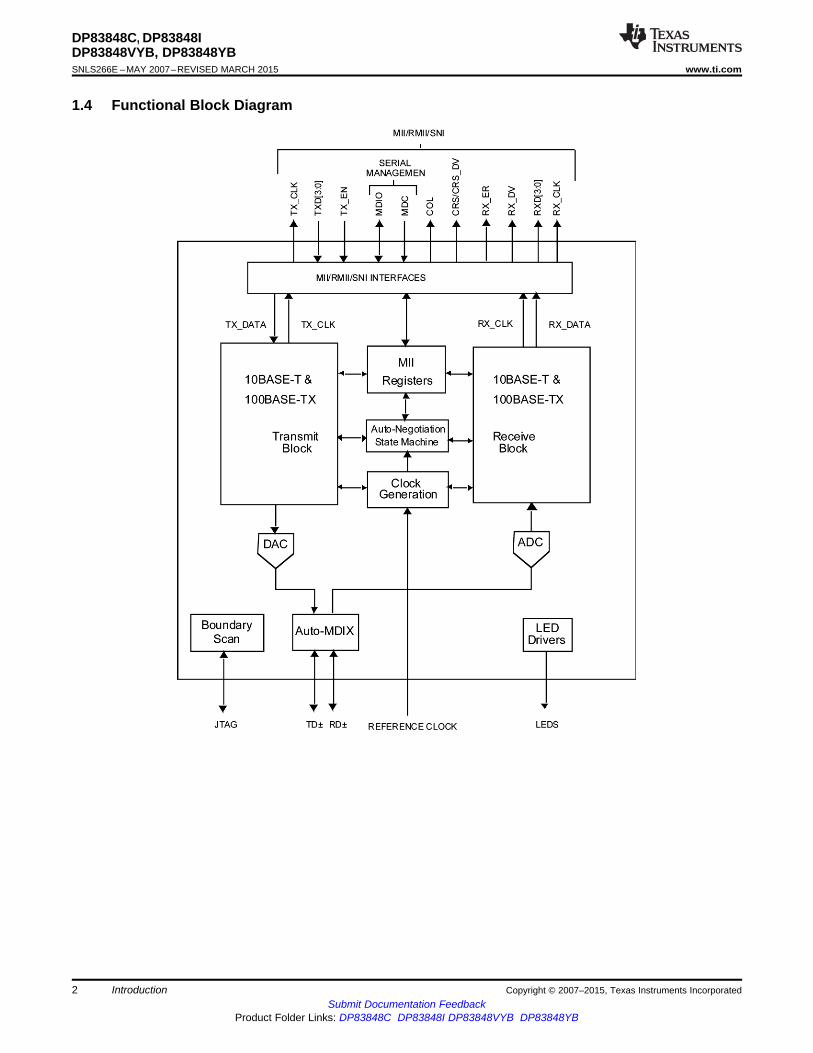


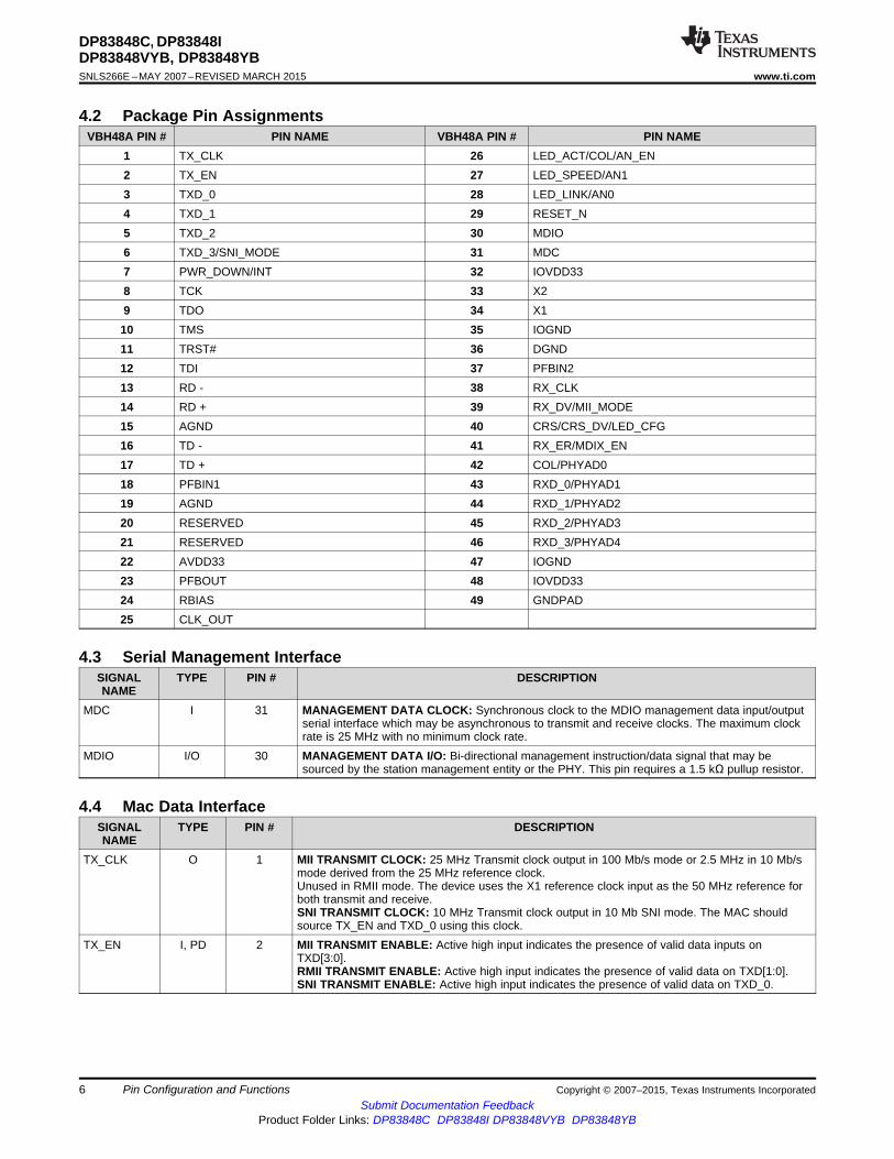

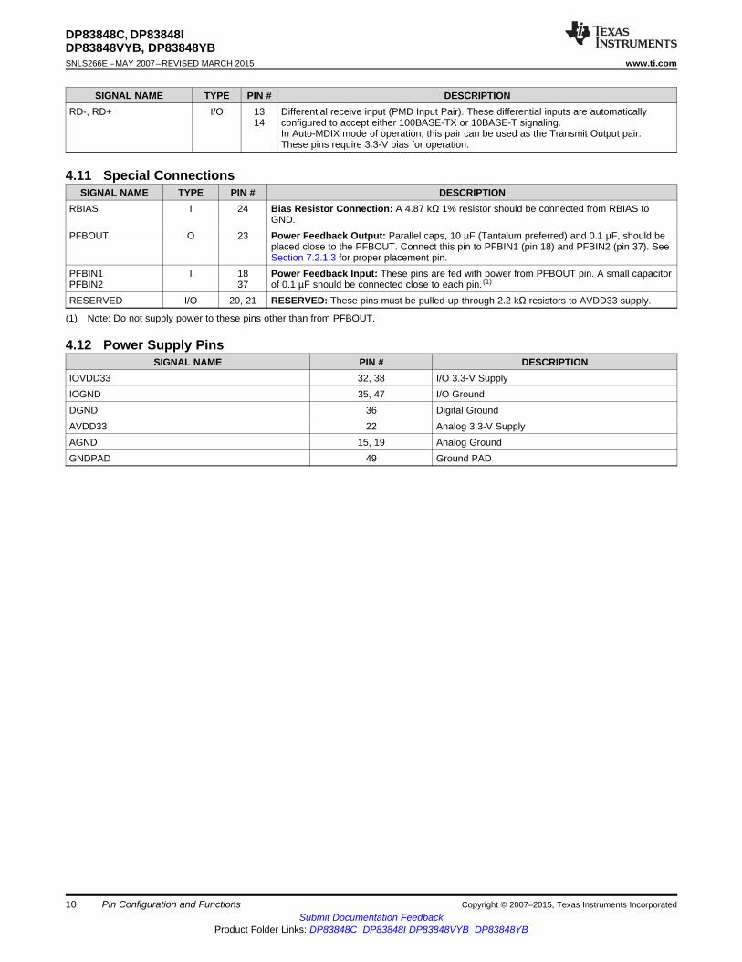
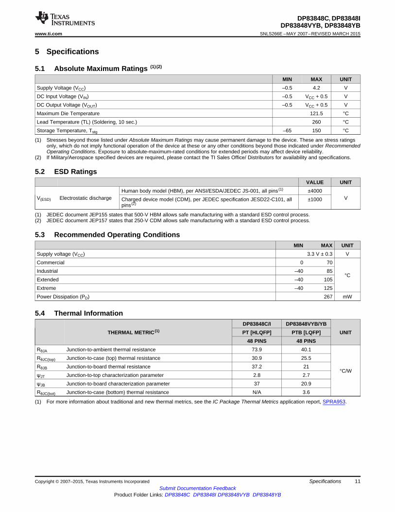


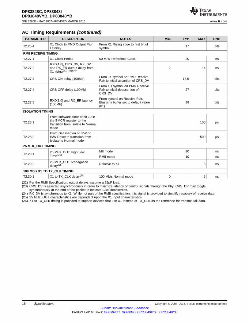

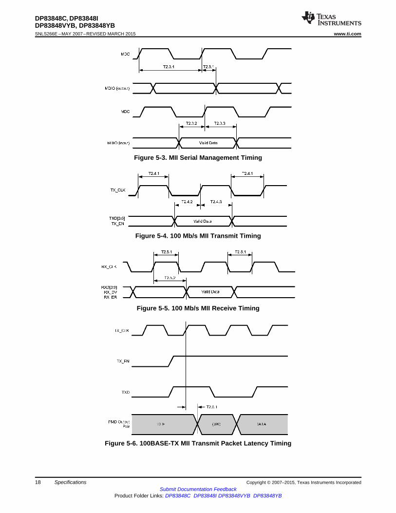

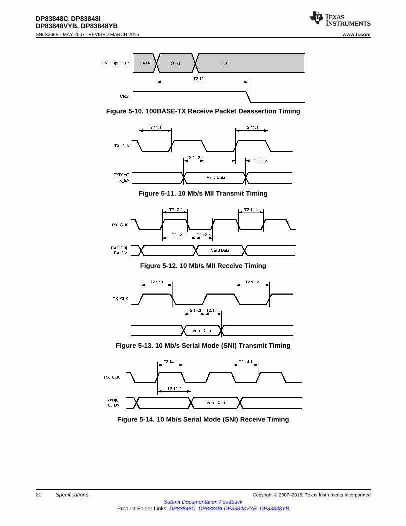


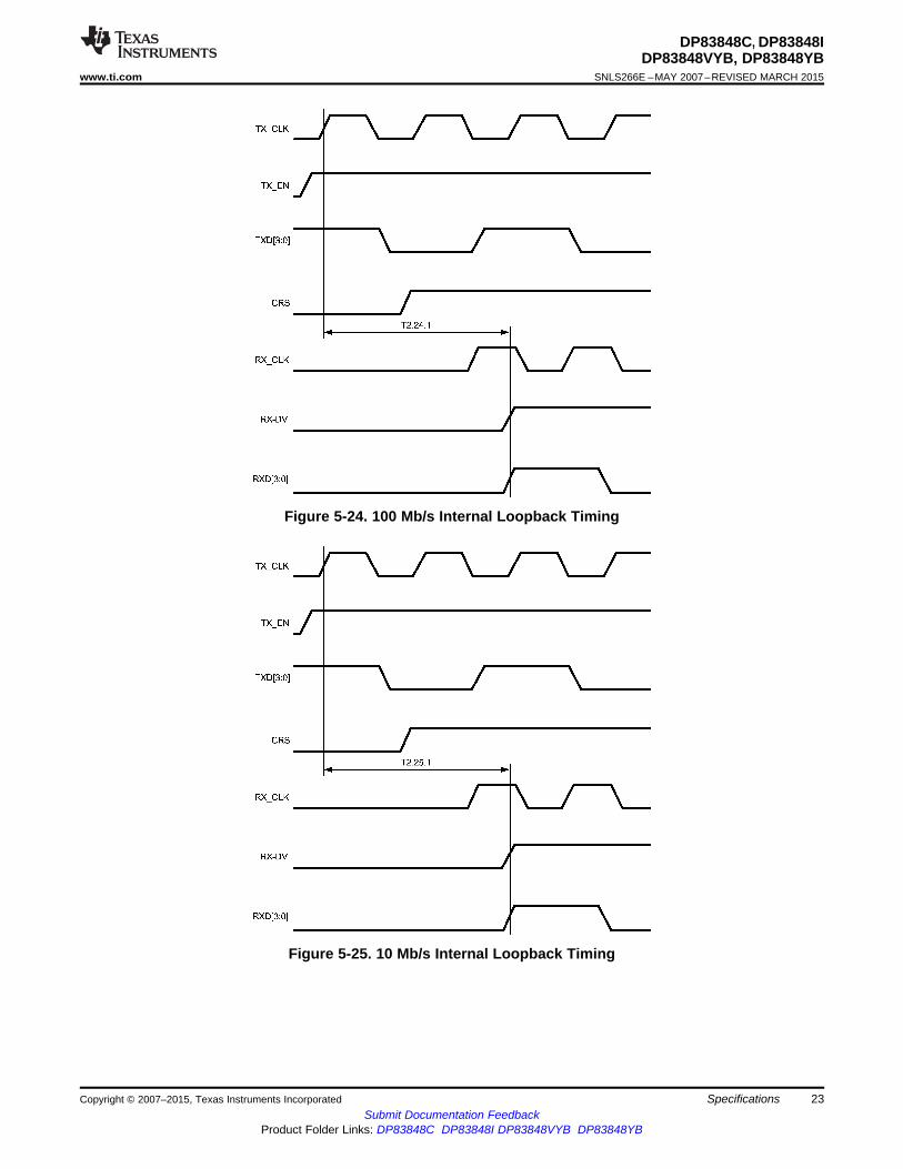
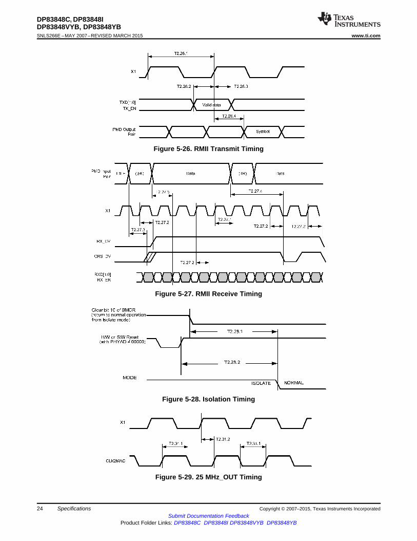
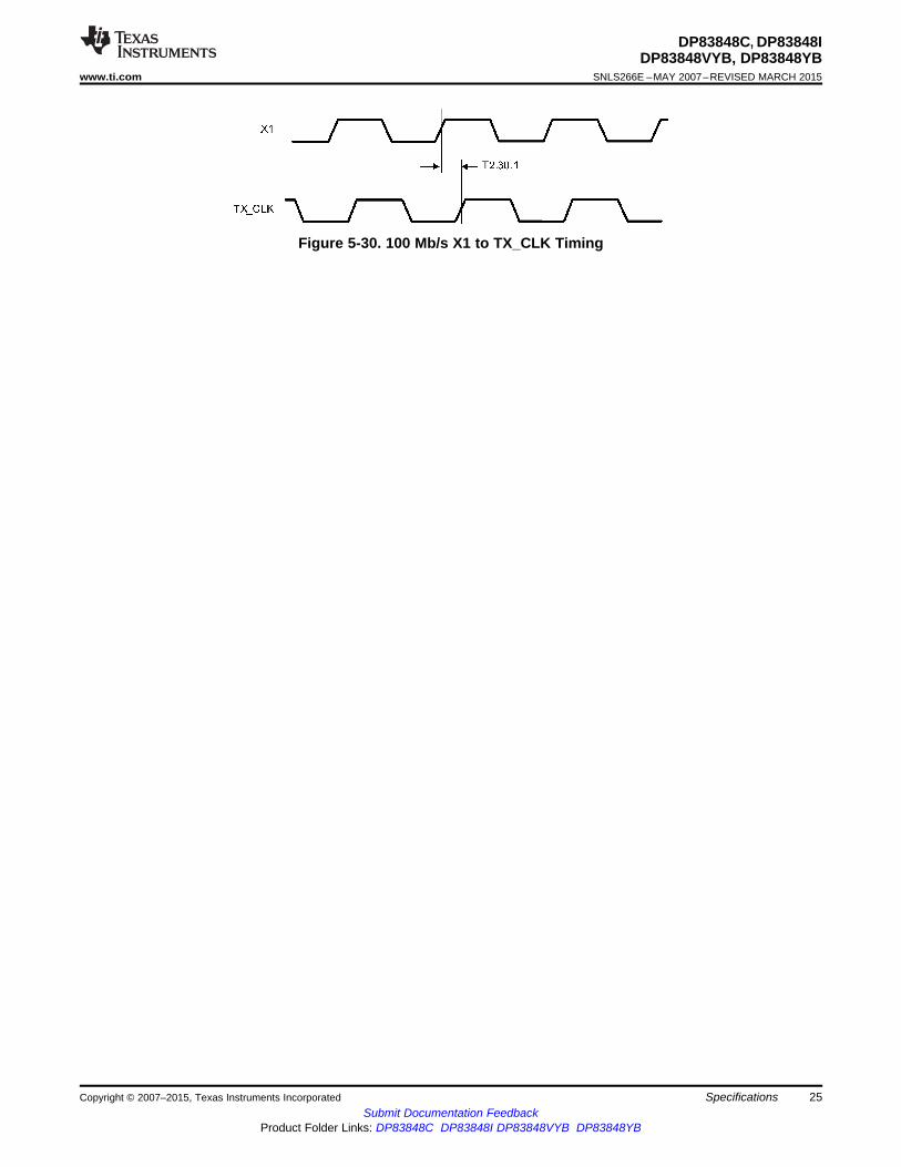

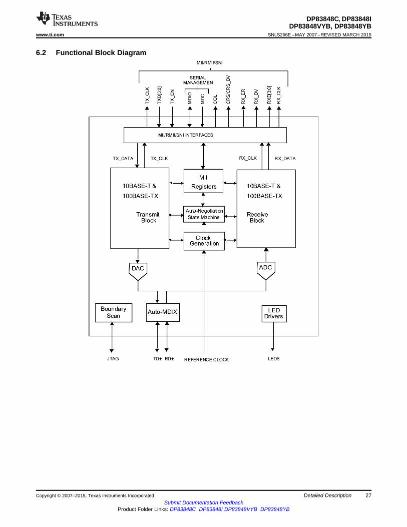


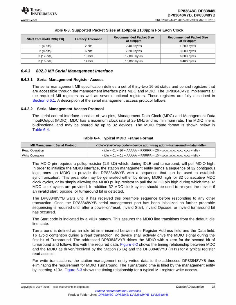
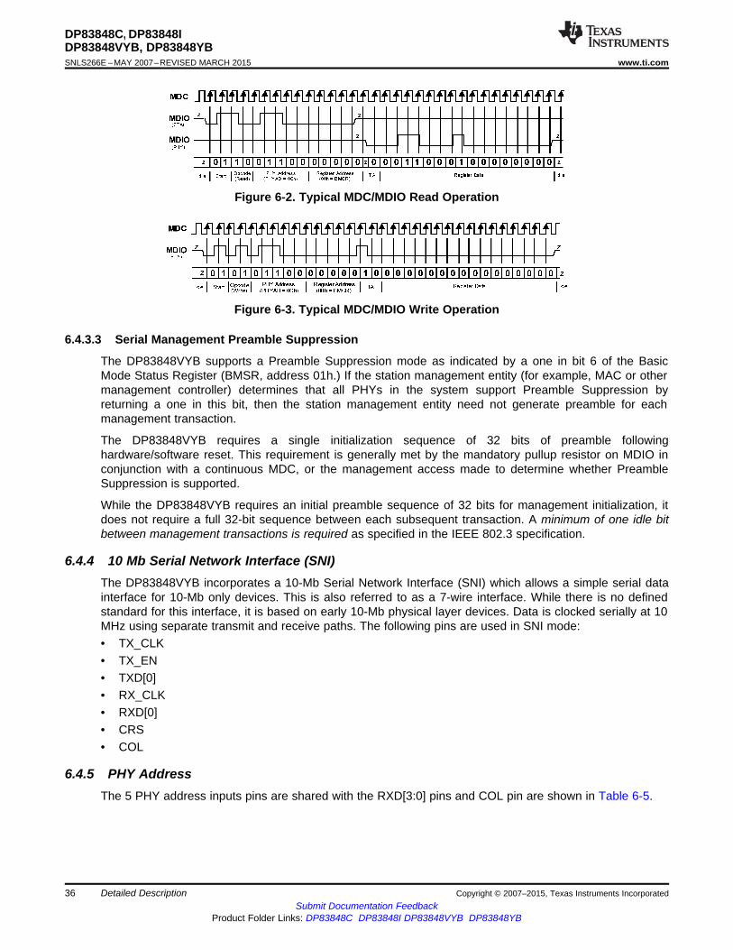


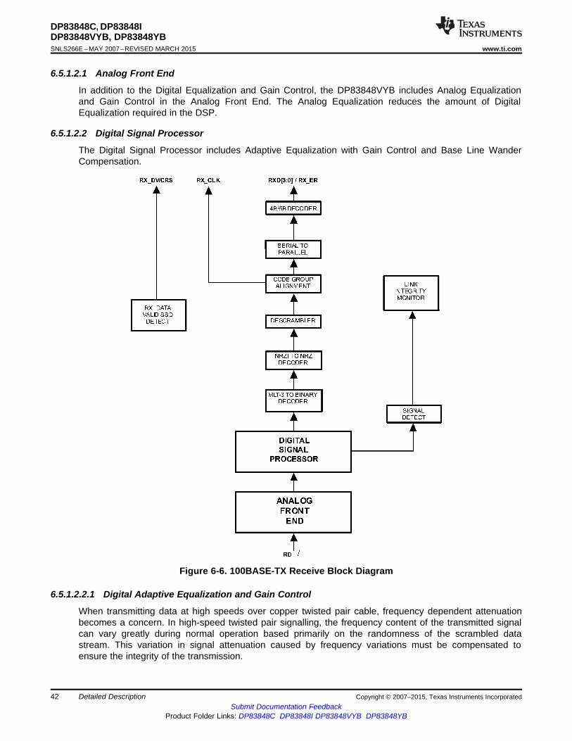
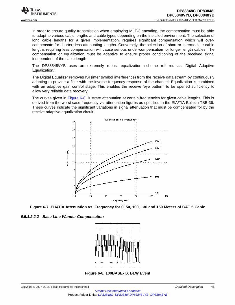


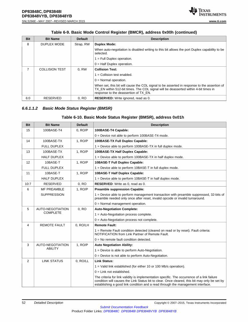
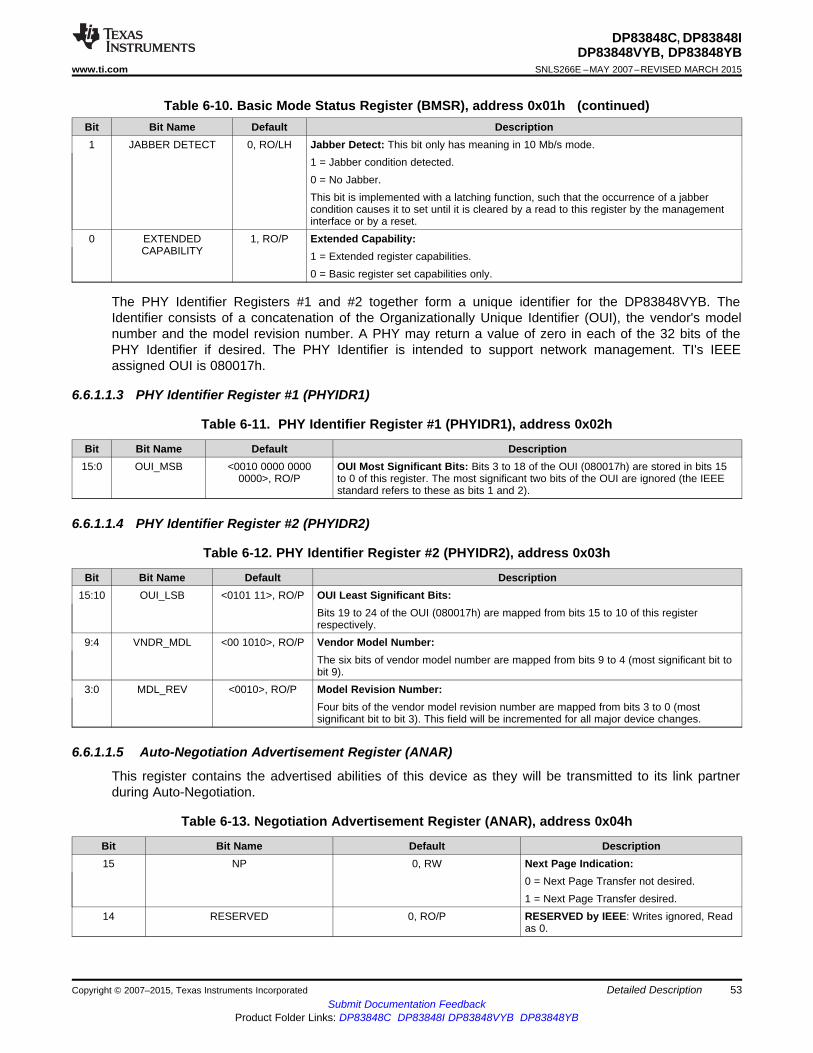
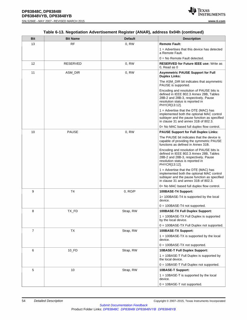


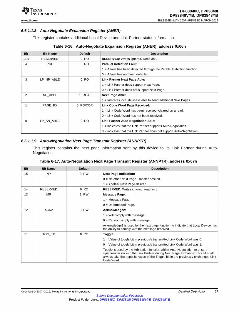

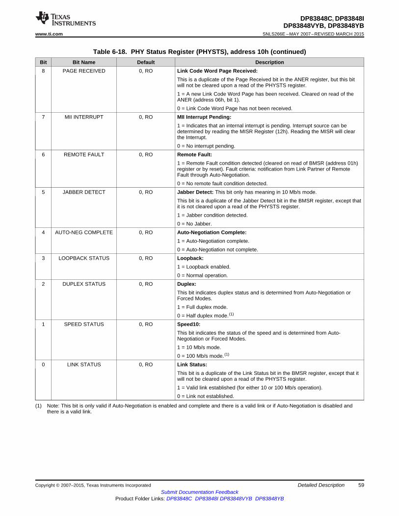


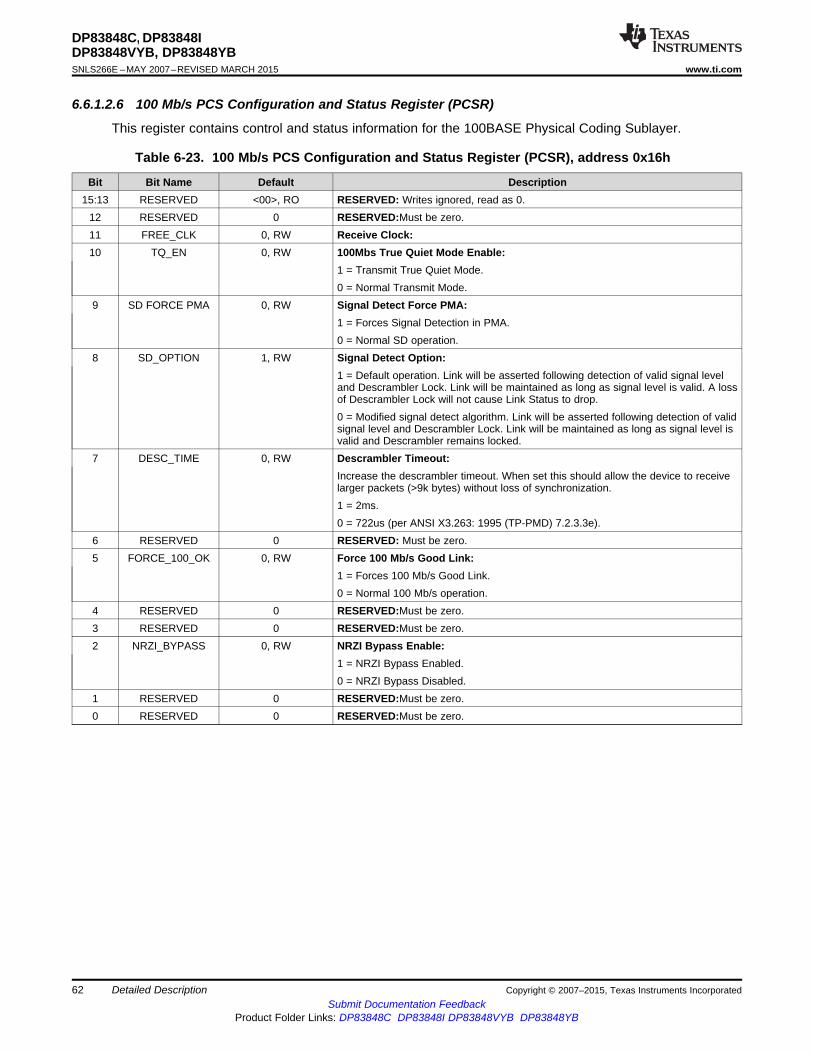
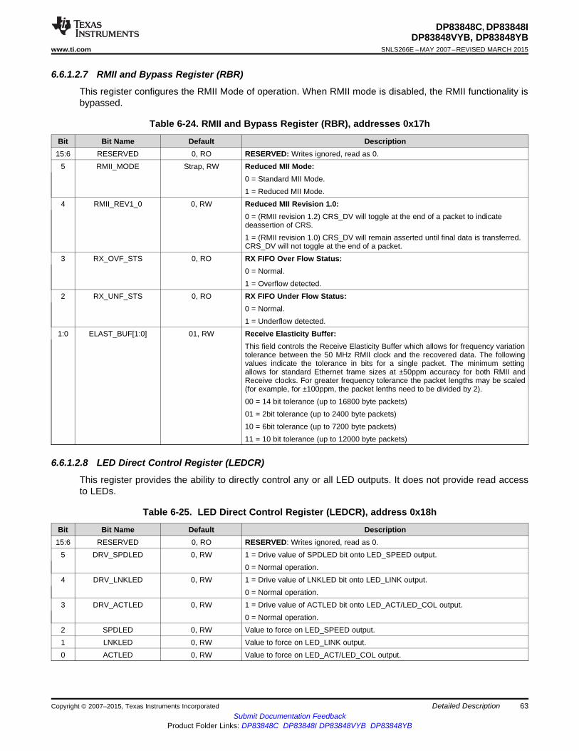


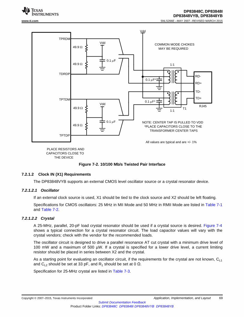
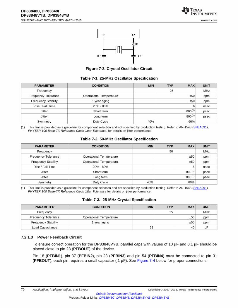

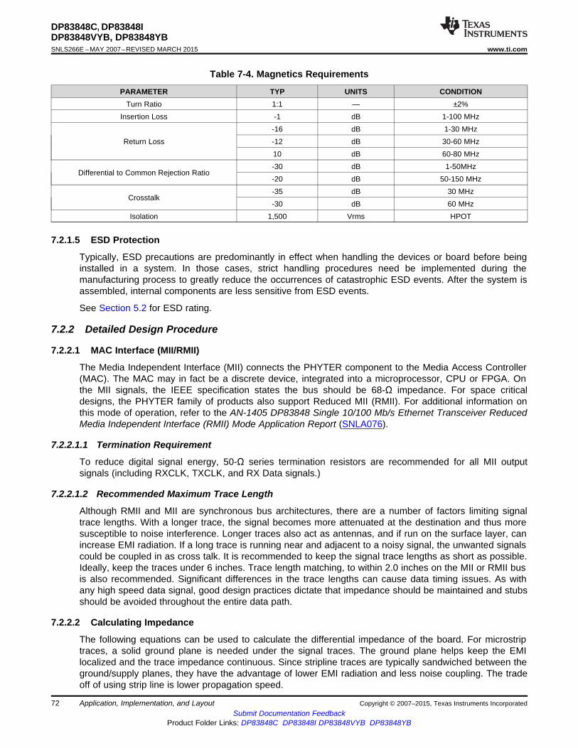


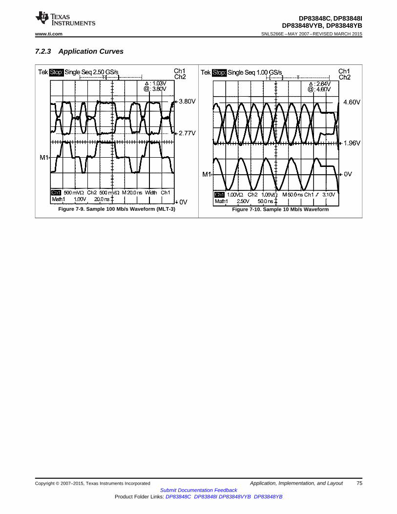
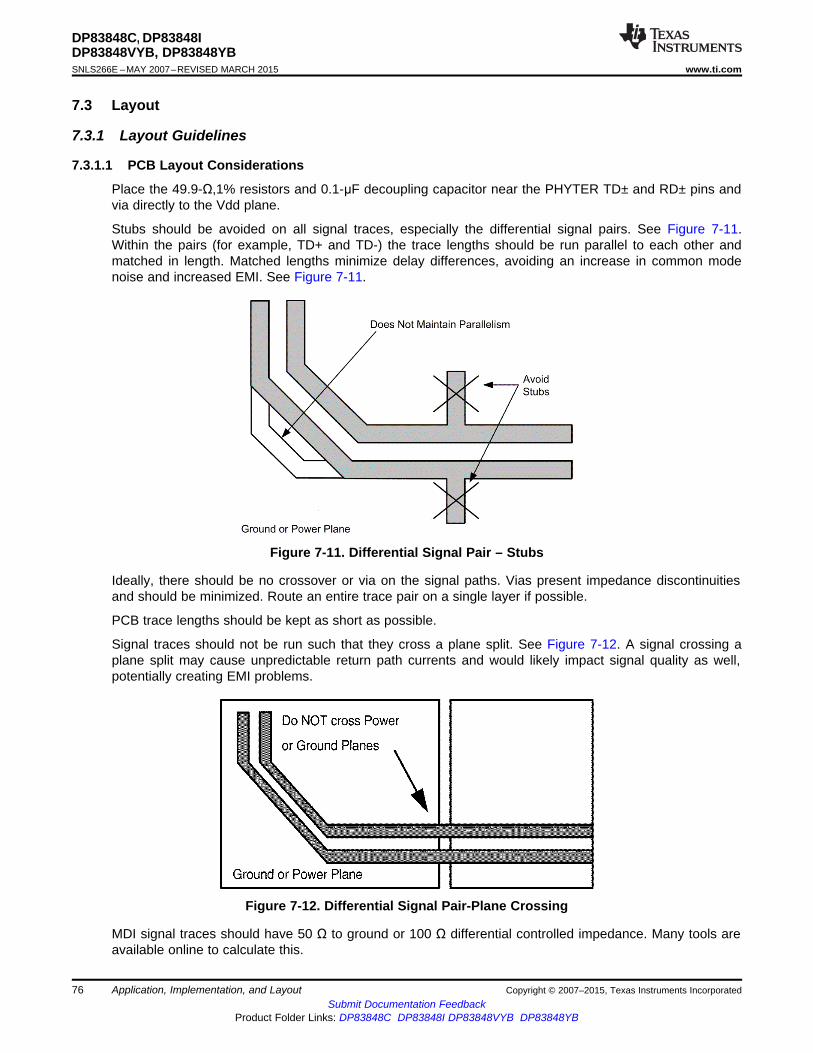
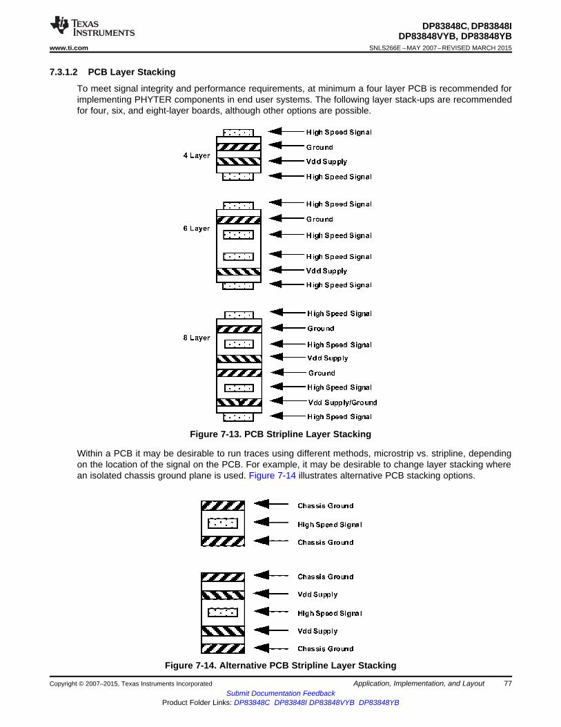


![`b TR QR b[N ZN[R N PN`V V[abVaVcN° · cvcv_ r[/n_pry\[n° 2y `ryy\ 0nanyv[n 2`a_nqn r` v[p\[sb[ qvoyr ]r_\ p\z\ vyb`a_nq\_n ¡un`]r[ `nq\ cn_vn_ qr r`avy\ qn_yr b[tv_\ n ab` p_rnpv\[r`,](https://static.documents.pub/doc/80x56/5e6fa98b5bb921735d49c099/b-tr-qr-bn-znr-n-pnv-vabvavcn-cvcv-rnpryn-2y-ryy-0nanyvn-2anqn.jpg)


![The Fallacy of Control - sapient.com · ÆI]^h ^hcÉi V hidgn VWdji iZX]cdad\n# >iÉh V hidgn d[ XjaijgZ!Ç hV^Y BVgi]V 9dgg^h VXi^c\ VhhdX^ViZ VYb^c^higVidg [dg i]Z](https://static.documents.pub/doc/80x56/5c65271009d3f2b26e8c4367/the-fallacy-of-control-aih-hcei-v-hidgn-vwdji-izxcdadn-ieh-v-hidgn.jpg)