Data Sheet. Types M0139S/R#120 to M0139S/R#180 Issue 2 Page 1 of 11 September 2016 Date:- 26 Sep, 2016 Data Sheet Issue:- 2 Soft Recovery Diode Type M0139S/R#120 to M0139S/R#180 Absolute Maximum Ratings VOLTAGE RATINGS MAXIMUM LIMITS UNITS VRRM Repetitive peak reverse voltage, (note 1) 1200-1800 V VRSM Non-repetitive peak reverse voltage, (note 1) 1300-1900 V OTHER RATINGS MAXIMUM LIMITS UNITS IF(AV)M Maximum average forward current, Tsink=55°C, (note 2) 139 A IF(AV)M Maximum average forward current. Tsink=100°C, (note 2) 58 A IF(RMS) Nominal RMS forward current, Tsink=25°C, (note 2) 288 A IF(d.c.) D.C. forward current, Tsink=25°C, (note 3) 219 A IFSM Peak non-repetitive surge tp=10ms, VRM=60%VRRM, (note 3) 2450 A IFSM2 Peak non-repetitive surge tp=10ms, VRM10V, (note 3) 2695 A I 2 t I 2 t capacity for fusing tp=10ms, VRM=60%VRRM, (note 3) 30×10 3 A 2 s I 2 t I 2 t capacity for fusing tp=10ms, VRM10V, (note 3) 36.5×10 3 A 2 s Tj op Operating temperature range -40 to +125 °C Tstg Storage temperature range -40 to +150 °C Notes:- 1) De-rating factor of 0.13% per °C is applicable for Tj below 25°C. 2) single phase; 50Hz, 180° half-sinewave. 3) Half-sinewave, 125°C Tj initial.
Transcript
Data Sheet. Types M0139S/R#120 to M0139S/R#180 Issue 2 Page 1 of 11 September 2016
Date:- 26 Sep, 2016
Data Sheet Issue:- 2
Soft Recovery Diode Type M0139S/R#120 to M0139S/R#180
Absolute Maximum Ratings
VOLTAGE RATINGS MAXIMUM
LIMITS UNITS
VRRM Repetitive peak reverse voltage, (note 1) 1200-1800 V
VRSM Non-repetitive peak reverse voltage, (note 1) 1300-1900 V
OTHER RATINGS MAXIMUM
LIMITS UNITS
IF(AV)M Maximum average forward current, Tsink=55°C, (note 2) 139 A
IF(AV)M Maximum average forward current. Tsink=100°C, (note 2) 58 A
IF(RMS) Nominal RMS forward current, Tsink=25°C, (note 2) 288 A
IF(d.c.) D.C. forward current, Tsink=25°C, (note 3) 219 A
IFSM Peak non-repetitive surge tp=10ms, VRM=60%VRRM, (note 3) 2450 A
IFSM2 Peak non-repetitive surge tp=10ms, VRM10V, (note 3) 2695 A
Notes:- 1) De-rating factor of 0.13% per °C is applicable for Tj below 25°C. 2) single phase; 50Hz, 180° half-sinewave. 3) Half-sinewave, 125°C Tj initial.
Soft Recovery Diode Types M0139S/R#120 to M0139S/R#180
Data Sheet. Types M0139S/R#120 to M0139S/R#180 Issue 2 Page 2 of 11 September 2016
Characteristics
PARAMETER MIN. TYP. MAX. TEST CONDITIONS (Note 1) UNITS
VFM Maximum peak forward voltage - - 1.60 IFM=280A V
Soft Recovery Diode Types M0139S/R#120 to M0139S/R#180
Data Sheet. Types M0139S/R#120 to M0139S/R#180 Issue 2 Page 3 of 11 September 2016
Notes on Ratings and Characteristics
1.0 Voltage Grade Table
Voltage Grade VRRM (V)
VRSM
(V) VR dc
(V)
12 1200 1300 810
18 1800 1900 1350
2.0 De-rating Factor A blocking voltage de-rating factor of 0.13% per °C is applicable to this device for Tj below 25°C. 3.0 ABCD Constants
These constants (applicable only over current range of VF characteristic in Figure 1) are the coefficients of
the expression for the forward characteristic given below:
FFFF IDICIBAV )ln(
where IF = instantaneous forward current. 4.0 Reverse recovery ratings
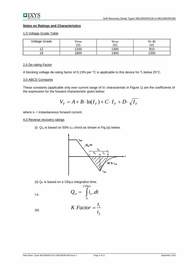
(i) Qra is based on 50% Irm chord as shown in Fig.(a) below.
(ii) Qrr is based on a 150s integration time.
I.e.
s
rrrr dtiQ
150
0
.
(iii) 2
1 t
tFactorK
Soft Recovery Diode Types M0139S/R#120 to M0139S/R#180
Data Sheet. Types M0139S/R#120 to M0139S/R#180 Issue 2 Page 4 of 11 September 2016
thJKMAXJSINK RfkETT )(
5.0 Reverse Recovery Loss
The following procedure is recommended for use where it is necessary to include reverse recovery loss.
From waveforms of recovery current obtained from a high frequency shunt (see Note 1) and reverse
voltage present during recovery, an instantaneous reverse recovery loss waveform must be constructed.
Let the area under this waveform be E joules per pulse. A new sink temperature can then be evaluated
from:
Where k = 0.2314 (°C/W)/s
E = Area under reverse loss waveform per pulse in joules (W.s.)
f = Rated frequency in Hz at the original sink temperature.
RthJK = d.c. thermal resistance (°C/W)
The total dissipation is now given by:
fEWW originaltot )()(
NOTE 1 - Reverse Recovery Loss by Measurement
This device has a low reverse recovered charge and peak reverse recovery current. When measuring the
charge, care must be taken to ensure that:
(a) AC coupled devices such as current transformers are not affected by prior passage of high
amplitude forward current.
(b) A suitable, polarised, clipping circuit must be connected to the input of the measuring oscilloscope
to avoid overloading the internal amplifiers by the relatively high amplitude forward current signal.
(c) Measurement of reverse recovery waveform should be carried out with an appropriate critically
damped snubber, connected across diode anode to cathode. The formula used for the calculation of this
snubber is shown below:
dtdi
S
r
C
VR
42
Where: Vr = Commutating source voltage
CS = Snubber capacitance
R = Snubber resistance
6.0 Snubber Components When selecting snubber components, care must be taken not to use excessively large values of snubber capacitor or excessively small values of snubber resistor. Such excessive component values may lead to device damage due to the large resultant values of snubber discharge current. If required, please consult the factory for assistance.
Soft Recovery Diode Types M0139S/R#120 to M0139S/R#180
Data Sheet. Types M0139S/R#120 to M0139S/R#180 Issue 2 Page 5 of 11 September 2016
7.0 Computer Modelling Parameters
7.1 Device Dissipation Calculations
T
AVTTT
AVrff
WrffVVI
2
2
00
2
4
Where VT0 =1.24V, rT = 1.28m
ff = form factor (normally unity for fast diode applications)
KMAXj
th
AV
TTT
R
TW
)(
7.2 Calculation of VF using ABCD Coefficients
The forward characteristic IF Vs VF, on page 6 is represented in two ways;
(i) the well established VT0 and rT tangent used for rating purposes and
((iiii)) a set of constants A, B, C, and D forming the coefficients of the representative equation for VF in
terms of IF given below:
FFFF IDICIBAV )ln(
The constants, derived by curve fitting software, are given in this report for both hot and cold
characteristics. The resulting values for VF agree with the true device characteristic over a current range,
which is limited to that plotted.
25°C Coefficients 125°C Coefficients
A 0.237145 -0.922256
B 0.2255735 0.5643498
C 0.63392×10⁻³ 1.189357×10⁻³
D -4.89596×10⁻³ -0.05985509
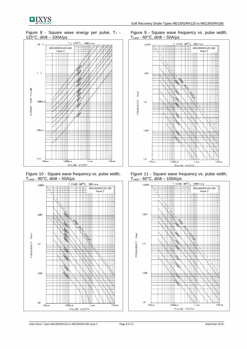
8.0 Frequency Ratings The curves illustrated in figures 4 to 12 are for guidance only and are superseded by the maximum ratings shown on page 1. 9.0 Square wave ratings These ratings are given for load component rate of rise of forward current of 100 and 500 A/µs. 10.0 Duty cycle lines The 100% duty cycle is represented on all the ratings by a straight line. Other duties can be included as parallel to the first.
Soft Recovery Diode Types M0139S/R#120 to M0139S/R#180
Data Sheet. Types M0139S/R#120 to M0139S/R#180 Issue 2 Page 6 of 11 September 2016
Disclaimer Notice - Information furnished is believed to be accurate and reliable. However, users should independently evaluate the suitability of and test each product selected for their own applications. Littelfuse products are not designed for, and may not be used in, all applications. Read complete Disclaimer Notice at www.littelfuse.com/disclaimer-electronics.


![Chapter 1: Diode circuits vtusolutionvtusolution.in/uploads/9/9/9/3/99939970/analog_electronic[15ec32].pdf · Chapter 1: Diode circuits ... • Diode testing • Zener diode • Diode](https://static.documents.pub/doc/80x56/5aedefea7f8b9a9031905d54/chapter-1-diode-circuits-vt-15ec32pdfchapter-1-diode-circuits-diode.jpg)


