Page 1
8/10/2019 solar cell tarun.pptx
http://slidepdf.com/reader/full/solar-cell-tarunpptx 1/12
Page 2
8/10/2019 solar cell tarun.pptx
http://slidepdf.com/reader/full/solar-cell-tarunpptx 2/12
Page 3
8/10/2019 solar cell tarun.pptx
http://slidepdf.com/reader/full/solar-cell-tarunpptx 3/12
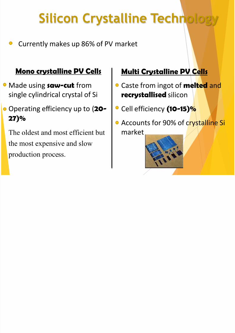
Photovoltaic Roadmap
1st Generation PV
Crystalline Silicon
2nd Generation PV
Thin Film
3rd Generation PV
Ultra-High Efficiency
Ultra-Low Cost
Source: European Commission meeting Dec. 2004
Page 4
8/10/2019 solar cell tarun.pptx
http://slidepdf.com/reader/full/solar-cell-tarunpptx 4/12
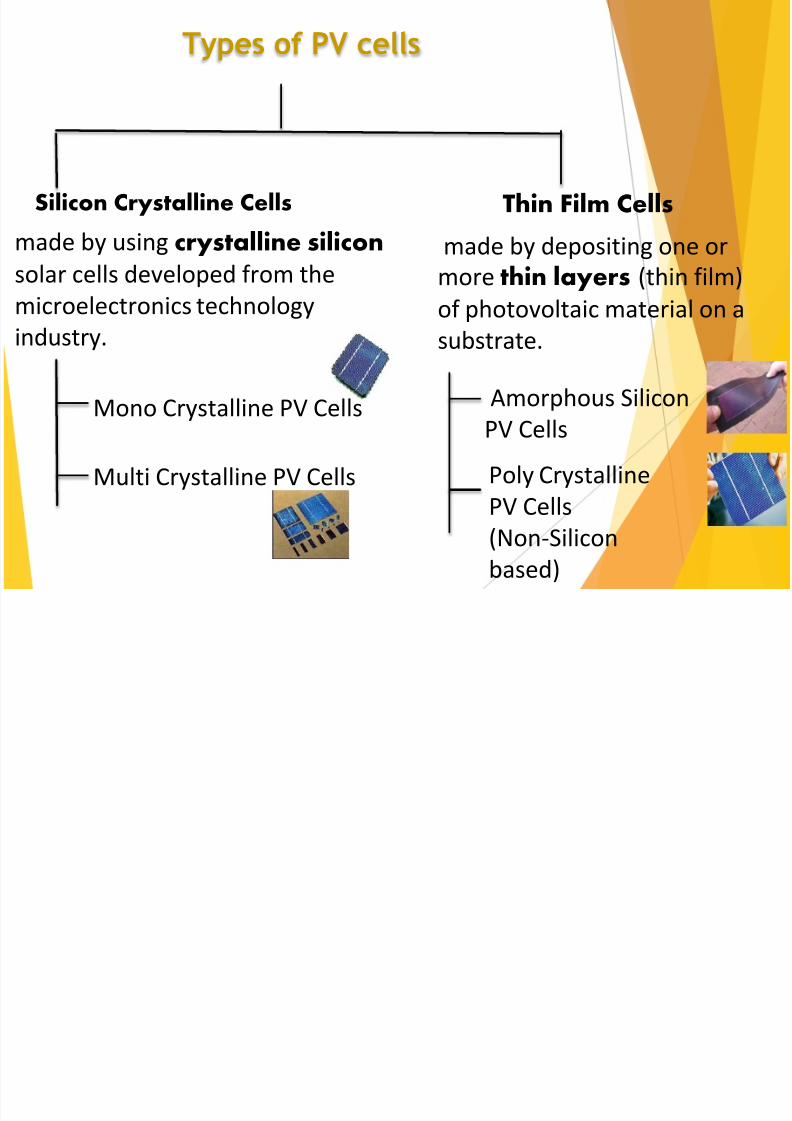
Types of PV cells
Silicon Crystalline Cells Thin Film Cells
made by using crystalline silicon
solar cells developed from themicroelectronics technology
industry.
made by depositing one or
more thin layers (thin film)of photovoltaic material on a
substrate.
Mono Crystalline PV Cells
Multi Crystalline PV Cells
Amorphous Silicon
PV Cells
Poly Crystalline
PV Cells
(Non-Silicon
based)
Page 5
8/10/2019 solar cell tarun.pptx
http://slidepdf.com/reader/full/solar-cell-tarunpptx 5/12
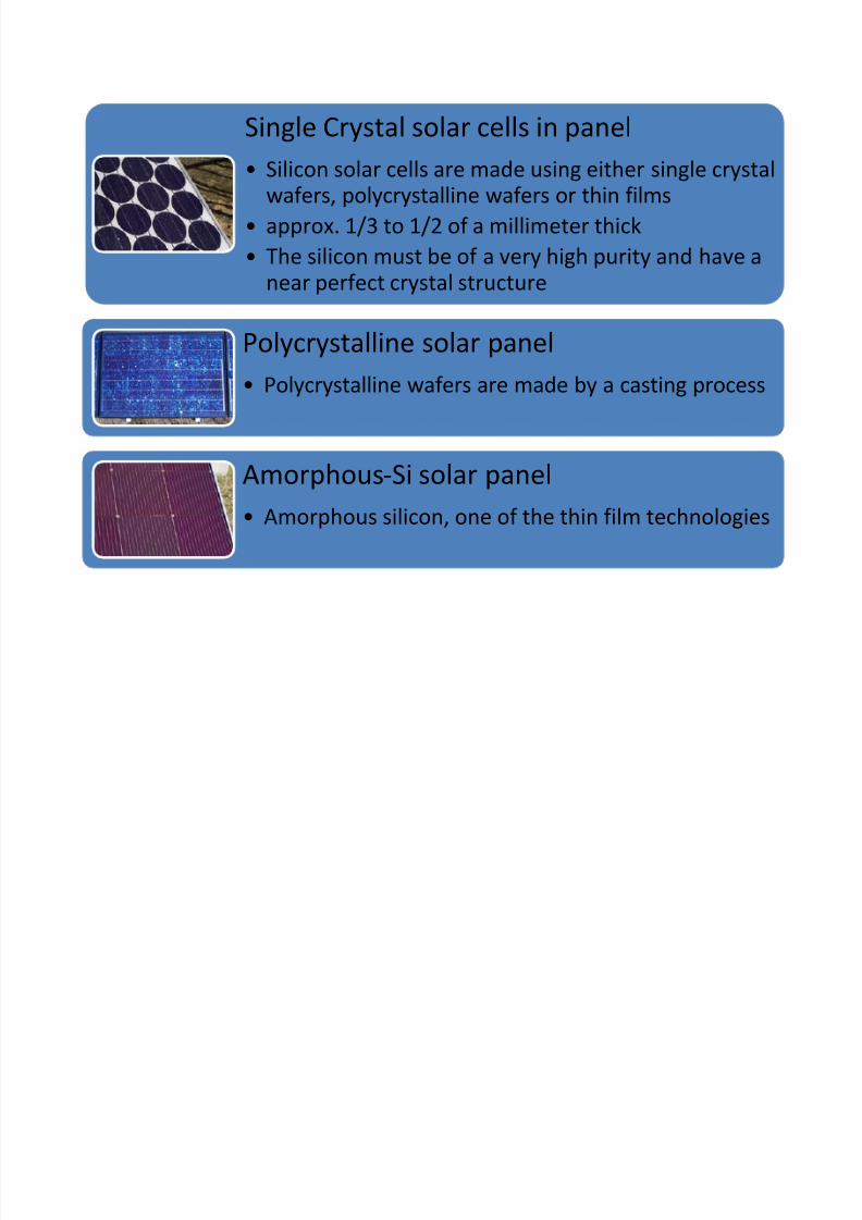
Single Crystal solar cells in panel
• Silicon solar cells are made using either single crystalwafers, polycrystalline wafers or thin films
• approx. 1/3 to 1/2 of a millimeter thick
• The silicon must be of a very high purity and have anear perfect crystal structure
Polycrystalline solar panel
• Polycrystalline wafers are made by a casting process
Amorphous-Si solar panel
• Amorphous silicon, one of the thin film technologies
Page 6
8/10/2019 solar cell tarun.pptx
http://slidepdf.com/reader/full/solar-cell-tarunpptx 6/12
FABRICATION
Single Crystal solar cells
Single crystal wafers are sliced from a large single crystal ingot
It is a very expensive process
The silicon must be of a very high purity and have a near perfect crystal
structure
Polycrystalline solar Polycrystalline wafers are made by a casting process
molten silicon is poured into a mould and allowed to set
Then it is sliced into wafers
it is not as efficient as monocrystalline cells
The lower efficiency is due to imperfections in the crystal structure resultingfrom the casting process
Amorphous-Si solar
Amorphous silicon is one of the thin film technologies
It is made by depositing silicon onto a glass substrate from a reactive gas
such as silane (SiH4)
Page 7
8/10/2019 solar cell tarun.pptx
http://slidepdf.com/reader/full/solar-cell-tarunpptx 7/12
Page 8
8/10/2019 solar cell tarun.pptx
http://slidepdf.com/reader/full/solar-cell-tarunpptx 8/12 e 8 / P
P A S o l a r P V D e s i g n I m p l e m e n t a t i o n O & M
M a r s h a l l I s l a n d s M a
r c h 3 1 - A p r i l 1 1 ,
2 0 0 8
8
• Crystal cell (Single crystal and Poly crystalline Silicon)
Single crystal Poly crystalline
1-1-2. Various type of PV cell
Formed by melting high purity
silicon like as Integrated Circuit
For mass production, cell is sliced
from roughly crystallized ingot.
Page 9
8/10/2019 solar cell tarun.pptx
http://slidepdf.com/reader/full/solar-cell-tarunpptx 9/12
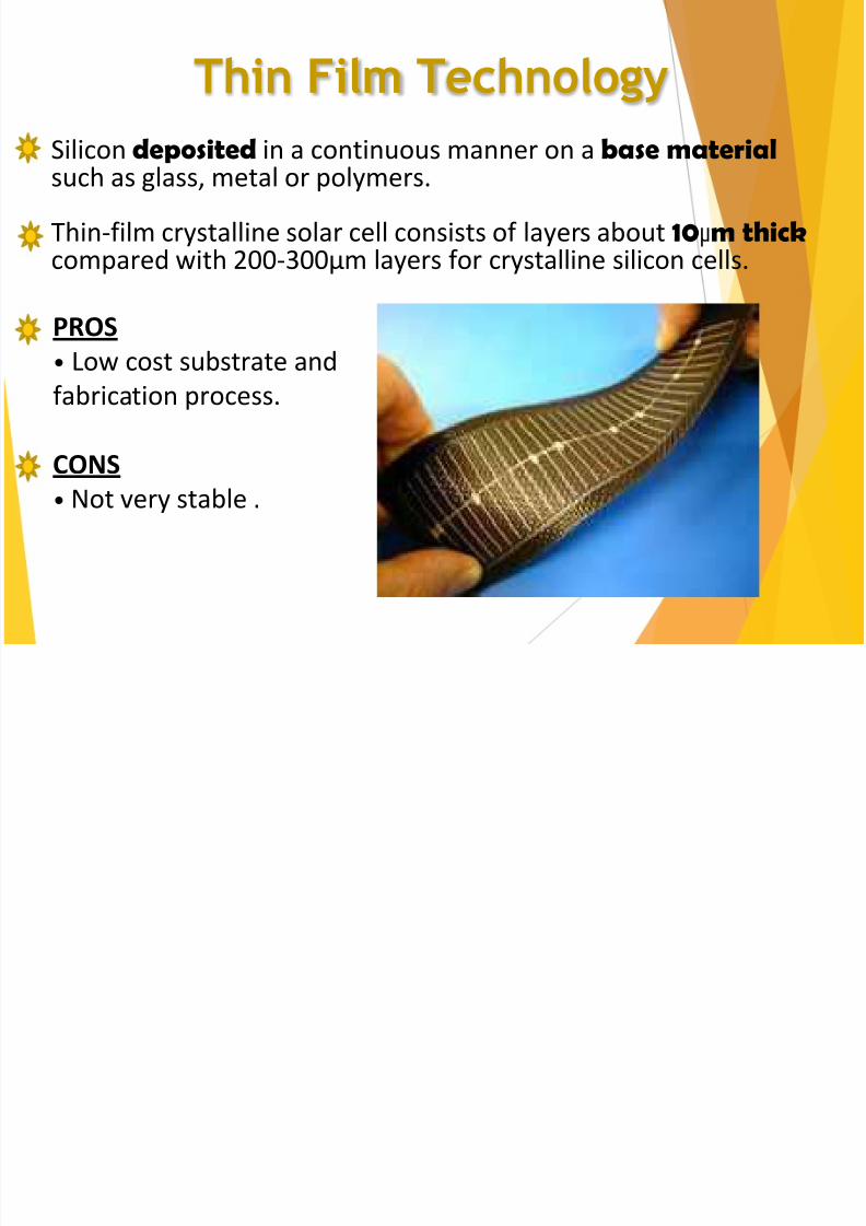
Thin Film Technology
Silicon deposited in a continuous manner on a base materialsuch as glass, metal or polymers.
Thin-film crystalline solar cell consists of layers about 10μm thickcompared with 200-300μm layers for crystalline silicon cells.
PROS
• Low cost substrate and
fabrication process.
CONS
• Not very stable .
Page 10
8/10/2019 solar cell tarun.pptx
http://slidepdf.com/reader/full/solar-cell-tarunpptx 10/12
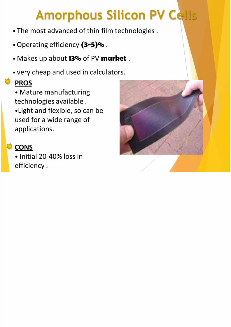
Amorphous Silicon PV Cells The most advanced of thin film technologies .
Operating efficiency (3-5)% .
Makes up about 13% of PV market .
very cheap and used in calculators.
PROS
• Mature manufacturing
technologies available .
•Light and flexible, so can be
used for a wide range ofapplications.
CONS
• Initial 20-40% loss in
efficiency .
Page 11
8/10/2019 solar cell tarun.pptx
http://slidepdf.com/reader/full/solar-cell-tarunpptx 11/12
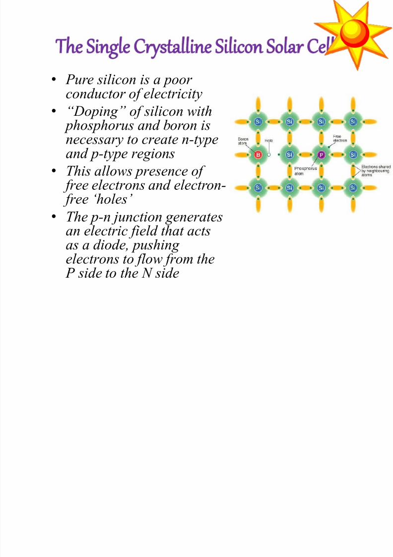
The Single rystalline Silicon Solar ell
• Pure silicon is a poorconductor of electricity
• “Doping” of silicon with phosphorus and boron is
necessary to create n-typeand p-type regions
• This allows presence of free electrons and electron-
free „holes‟ • The p-n junction generates
an electric field that actsas a diode, pushingelectrons to flow from the
P side to the N side
Page 12
8/10/2019 solar cell tarun.pptx
http://slidepdf.com/reader/full/solar-cell-tarunpptx 12/12
Poly Crystalline PV Cells( Non – Silicon Based Technology )
PROS
16% laboratory efficiency
6-9% module efficiencyCONS
Immature manufacturing process
Unlike most other II/IV material CdTe exhibits direct band
gap of 1.4eV and high absorption coefficient