Performance evaluation of a GaInP/GaAs solar cell structure with the integration of AlGaAs tunnel junction Yunus Özen a,b,n , Nihan Akın a,b , Barış Kınacı c , Süleyman Özçelik a,b a Photonics Application and Research Center, Gazi University, 06500 Ankara, Turkey b Department of Physics, Faculty of Science, Gazi University, 06500 Ankara, Turkey c Department of Physics, Faculty of Science, Istanbul University, 34134 Vezneciler Istanbul, Turkey article info Article history: Received 12 December 2014 Received in revised form 28 December 2014 Accepted 13 January 2015 Keywords: GaInP/GaAs solar cell AlGaAs tunnel junction The energy conversion efficiency abstract A GaInP/GaAs solar cell structure with AlGaAs tunnel junction was grown on p-type (1 0 0)-oriented GaAs substrate by a solid-source molecular beam epitaxy technique. The structural and morphological properties of the GaInP/GaAs solar cell structure have been evaluated by means of secondary ion mass spectrometry and atomic force microscopy measurements. In addition, the GaInP/GaAs solar cell device was fabricated to obtain electrical output parameters of the cells. For this purpose, the current–voltage measurements of solar cell devices were carried out at room temperature under both dark and air mass 1.5 global radiation (AM1.5) using solar simulator. In addition, the electrical output parameters of the GaInP/GaAs solar cell structure with the AlGaAs tunnel junction are compared with the GaInP/GaAs solar cell structure without the AlGaAs tunnel junction, and it is found that the integration of the tunnel junction into a solar cell structure improves the device performance by 48%. & 2015 Elsevier B.V. All rights reserved. 1. Introduction According to literature, solar cells (SCs) can be divided into four groups: (1) silicon-based SCs such as mono-crystalline silicon, and poly-crystalline silicon SCs [1–7], (2) thin film SCs such as amorphous silicon, cadmium–telluride, and copper–indium–gal- lium–de selenide SCs [8–15], and (3) III–V group SCs such as quantum well, and multi-junction SCs [16–29], (4) other SCs such as organic, dye sensitized and perovskite SCs [30–33]. There has been an increasing interest on the research and development of multi-junction III–V group SCs due to a higher efficiency compared to other groups SCs. Currently, the studies on these SCs are mainly focused on the performance evaluation [34–38]. Multi-junction SCs are sensitive to radiation of different wavelengths. A top cell is responsive to shorter wavelengths, whereas a bottom cell is responsive to longer wavelengths. In configuration, wider bandgap materials are used for the top cells since they absorb short wavelengths. Thus, it allows the longer wavelength radiation to penetrate deeper into the device where it can be converted into electrical energy. The commonly used highest-performing multi- junction cells use III–V compound semiconductors with direct bandgaps [39]. III–V Group ternary alloy materials, such as AlGaAs, InGaAs, InGaN and GaInP, were widely used as the top cell of SCs [18,20,22,25,27,29,34–38]. Among these materials, GaInP ternary alloy is an essential material for high efficiency SCs as it absorbs the visible part of the solar spectrum [40]. In addition, GaAs binary compound (bandgap: 1.42 eV) absorbs near-infrared part of the solar spectrum. When the Ga composition ratio is approximately 51% of the GaInP/GaAs structure, GaInP ternary alloy grows on a GaAs substrate with lattice-match, and this structure has great technological importance [40–42]. The GaInP/GaAs SC structure will continue to be the focus of attention in the photovoltaic works as it absorbs the large part of the solar spectrum. Tunnel junctions (TJs) are highly doped p–n diodes which allow for quantum mechanical tunneling through their narrow depletion regions. TJs are very crucial for multi-junction SCs, and they have properties such as a relatively optically transparent and low resistance [43]. According to the tunneling effect, the electron does not need extra energy for tunneling from the bottom of the conduction band to the top of the valence band. In addition, heavily doped AlGas, InGaP, GaAs, etc. are selected as TJs in III–V group SCs [27]. Several researches have studied the SCs structure with an integration of TJ [27,28,34]. Siyu et al. [27] examined the characteristics of the TJ, the material used in the TJ, the compen- sation of the TJ to the overall cell’s characteristics, the TJs’ influence on the current density of sub-cells and the efficiency increase. Wheelden et al. [28] investigated four different TJ designs Contents lists available at ScienceDirect journal homepage: www.elsevier.com/locate/solmat Solar Energy Materials & Solar Cells http://dx.doi.org/10.1016/j.solmat.2015.01.021 0927-0248/& 2015 Elsevier B.V. All rights reserved. n Corresponding author at: Photonics Application and Research Center, Gazi University, 06500 Ankara, Turkey. Tel.: þ90 312 202 12 79; fax: þ90 312 212 22 79. E-mail addresses: [email protected], [email protected](Y. Özen). Solar Energy Materials & Solar Cells 137 (2015) 1–5
Transcript
Performance evaluation of a GaInP/GaAs solar cell structurewith the integration of AlGaAs tunnel junction
Yunus Özen a,b,n, Nihan Akın a,b, Barış Kınacı c, Süleyman Özçelik a,b
a Photonics Application and Research Center, Gazi University, 06500 Ankara, Turkeyb Department of Physics, Faculty of Science, Gazi University, 06500 Ankara, Turkeyc Department of Physics, Faculty of Science, Istanbul University, 34134 Vezneciler Istanbul, Turkey
a r t i c l e i n f o
Article history:Received 12 December 2014Received in revised form28 December 2014Accepted 13 January 2015
Keywords:GaInP/GaAs solar cellAlGaAs tunnel junctionThe energy conversion efficiency
a b s t r a c t
A GaInP/GaAs solar cell structure with AlGaAs tunnel junction was grown on p-type (1 0 0)-orientedGaAs substrate by a solid-source molecular beam epitaxy technique. The structural and morphologicalproperties of the GaInP/GaAs solar cell structure have been evaluated by means of secondary ion massspectrometry and atomic force microscopy measurements. In addition, the GaInP/GaAs solar cell devicewas fabricated to obtain electrical output parameters of the cells. For this purpose, the current–voltagemeasurements of solar cell devices were carried out at room temperature under both dark and air mass1.5 global radiation (AM1.5) using solar simulator. In addition, the electrical output parameters of theGaInP/GaAs solar cell structure with the AlGaAs tunnel junction are compared with the GaInP/GaAs solarcell structure without the AlGaAs tunnel junction, and it is found that the integration of the tunneljunction into a solar cell structure improves the device performance by 48%.
& 2015 Elsevier B.V. All rights reserved.
1. Introduction
According to literature, solar cells (SCs) can be divided into fourgroups: (1) silicon-based SCs such as mono-crystalline silicon, andpoly-crystalline silicon SCs [1–7], (2) thin film SCs such asamorphous silicon, cadmium–telluride, and copper–indium–gal-lium–de selenide SCs [8–15], and (3) III–V group SCs such asquantum well, and multi-junction SCs [16–29], (4) other SCs suchas organic, dye sensitized and perovskite SCs [30–33]. There hasbeen an increasing interest on the research and development ofmulti-junction III–V group SCs due to a higher efficiency comparedto other groups SCs. Currently, the studies on these SCs are mainlyfocused on the performance evaluation [34–38]. Multi-junctionSCs are sensitive to radiation of different wavelengths. A top cell isresponsive to shorter wavelengths, whereas a bottom cell isresponsive to longer wavelengths. In configuration, wider bandgapmaterials are used for the top cells since they absorb shortwavelengths. Thus, it allows the longer wavelength radiation topenetrate deeper into the device where it can be converted intoelectrical energy. The commonly used highest-performing multi-junction cells use III–V compound semiconductors with direct
bandgaps [39]. III–V Group ternary alloy materials, such as AlGaAs,InGaAs, InGaN and GaInP, were widely used as the top cell of SCs[18,20,22,25,27,29,34–38]. Among these materials, GaInP ternaryalloy is an essential material for high efficiency SCs as it absorbsthe visible part of the solar spectrum [40]. In addition, GaAs binarycompound (bandgap: 1.42 eV) absorbs near-infrared part of thesolar spectrum. When the Ga composition ratio is approximately51% of the GaInP/GaAs structure, GaInP ternary alloy grows on aGaAs substrate with lattice-match, and this structure has greattechnological importance [40–42]. The GaInP/GaAs SC structurewill continue to be the focus of attention in the photovoltaic worksas it absorbs the large part of the solar spectrum.
Tunnel junctions (TJs) are highly doped p–n diodes which allowfor quantum mechanical tunneling through their narrow depletionregions. TJs are very crucial for multi-junction SCs, and they haveproperties such as a relatively optically transparent and lowresistance [43]. According to the tunneling effect, the electrondoes not need extra energy for tunneling from the bottom of theconduction band to the top of the valence band. In addition,heavily doped AlGas, InGaP, GaAs, etc. are selected as TJs in III–Vgroup SCs [27]. Several researches have studied the SCs structurewith an integration of TJ [27,28,34]. Siyu et al. [27] examined thecharacteristics of the TJ, the material used in the TJ, the compen-sation of the TJ to the overall cell’s characteristics, the TJs’influence on the current density of sub-cells and the efficiencyincrease. Wheelden et al. [28] investigated four different TJ designs
Contents lists available at ScienceDirect
journal homepage: www.elsevier.com/locate/solmat
Solar Energy Materials & Solar Cells
http://dx.doi.org/10.1016/j.solmat.2015.01.0210927-0248/& 2015 Elsevier B.V. All rights reserved.
n Corresponding author at: Photonics Application and Research Center, GaziUniversity, 06500 Ankara, Turkey. Tel.: þ90 312 202 12 79; fax: þ90 312 212 22 79.
Solar Energy Materials & Solar Cells 137 (2015) 1–5
(AlGaAs/AlGaAs, GaAs/GaAs, AlGaAs/InGaP, AlGaAs/GaAs) formulti-junction SCs under high concentration to determine thepeak tunneling current and resistance change as a function of thedoping concentration. They clearly demonstrated that the advan-tages of the AlGaAs/GaAs and the AlGaAs/AlGaAs TJ design morethan the GaAs/GaAs and the AlGaAs/InGaP TJ design. Samberget al. [34] investigated the effect of the heterojunction interface onthe performance of high bandgap InGaP:Te/AlGaAs:C TJs and thecompared experimental results with the modeling results arereasonable. They showed that the high tunneling current achievedin these TJs with a voltage drop of only a few mV across thejunction can allow multi-junction SCs to operate at higher con-centrations. As a result, TJ plays a crucial role in the multi-junctioncell design, and they have an essential impact on the performanceand reliability of the devices.
In our previous study [37], the GaInP/GaAs SC structure wasgrown using the molecular beam epitaxy (MBE) technique. Weinvestigated the structural, optical and morphological propertiesof GaInP/GaAs solar cell (SC) structure, and we also obtained theenergy conversion efficiency value as 9.13%. In the light of ourprevious study, the purpose of this research is to examine theeffect of AlGaAs TJ on the cell’s electrical output parameters of the
GaInP/GaAs SC structure. Thus, this paper is organized as follows:the GaInP/GaAs SC structure was grown on p-type (1 0 0)-orientedGaAs substrate by MBE. The secondary ion mass spectrometry(SIMS) measurement was preferred to analyze the depth profile ofthe GaInP/GaAs SC structure. Thus, not only main elements (Ga, In,Al, As and P) were detected, but also dopant elements (Si and Be)in the epi-layer. The morphology and the surface roughness weredetermined using atomic force microscopy (AFM) measurements.In addition, device parameters such as open-circuit voltage (Voc),short-circuit current (Isc), fill factor (FF) and energy conversionefficiency (η) of GaInP/GaAs SC structure with AlGaAs TJ wereextracted from the current–voltage (I–V) characteristics.
2. Experimental method
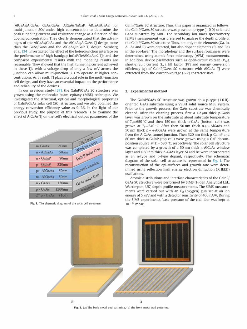
The GaInP/GaAs SC structure was grown on a p-type (1 0 0)-oriented GaAs substrate using a V80H solid source MBE system.Prior to the growth process, the GaAs substrate was chemicallycleaned. After the cleaning process, first a 1.2 mm thick p-GaAslayer was grown on the substrate at about substrate temperatureof Ts¼650 1C and then 150 nm thick n-GaAs (bottom cell) wasgrown at Ts¼640 1C. After then 50 nm thick nþþAlGaAs and50 nm thick pþþAlGaAs were grown at the same temperaturefrom the AlGaAs tunnel junction. Then 320 nm thick p-GaInP and80 nm thick n-GaInP (top cell) were grown using a GaP decom-position source at Ts¼530 1C, respectively. The solar cell structurewas completed by a growth of a 50 nm thick n-AlGaAs windowlayer and a 60 nm thick n-GaAs layer. Si and Be were incorporatedas an n-type and p-type dopant, respectively. The schematicdiagram of the solar cell structure is represented in Fig. 1. Thereconstruction of the epi-surfaces and growth rate were deter-mined using reflection high energy electron diffraction (RHEED)oscillations.
Atomic distributions and interface characteristics of the GaInP/GaAs SC structure were performed by SIMS (Hiden Analytical Ltd.,Warrington, UK) depth profile measurements. The SIMS measure-ments were carried out with an O2 (oxygen) gun set at an ionenergy of 5 keV and with a detector sensitivity of 400 nA/V. Duringthe SIMS experiments, base pressure of the chamber was kept at10�10 mbar.Fig. 1. The shematic diagram of the solar cell structure.
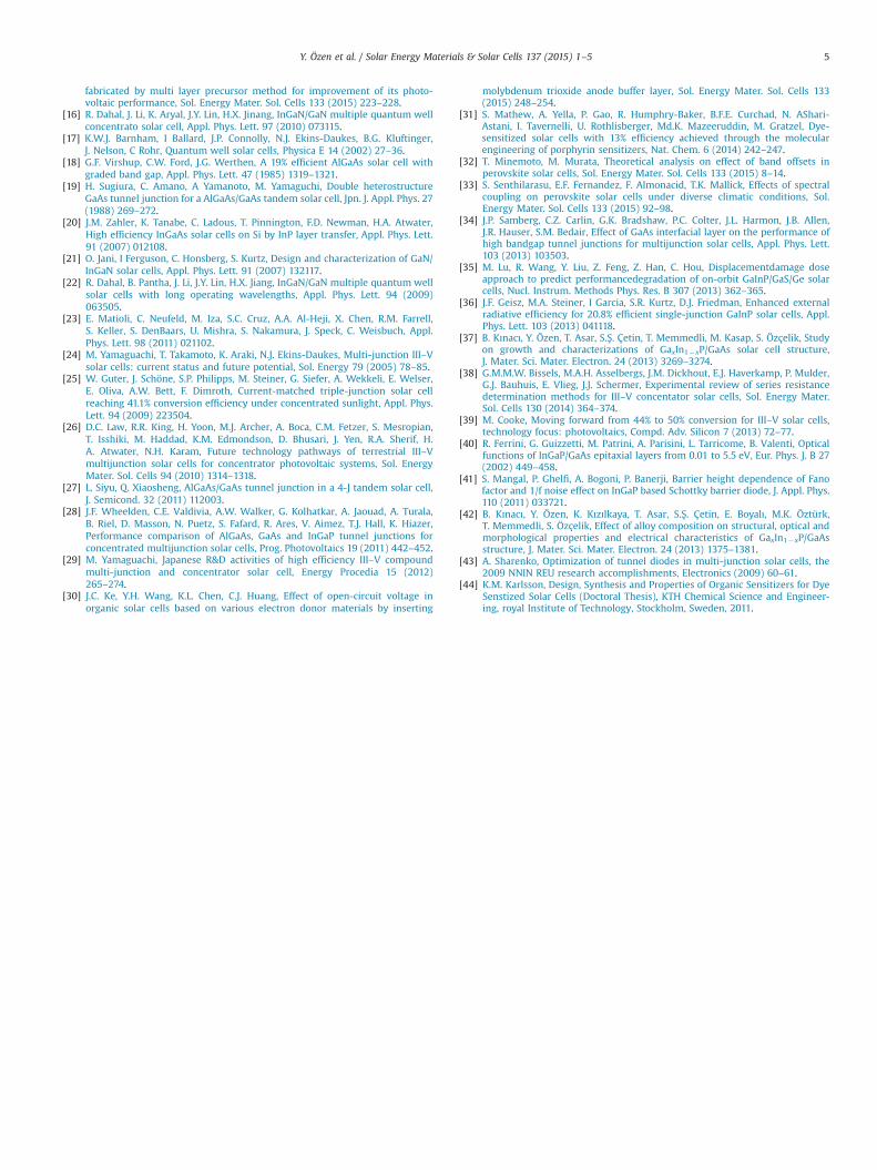
Fig. 2. (a) The back metal pad pattering, (b) the front metal pad pattering.
Y. Özen et al. / Solar Energy Materials & Solar Cells 137 (2015) 1–52
Morphological properties of the GaInP/GaAs SC structure werecharacterized at room temperature (RT) using high performanceAFM (Nano Magnetics Instruments Ltd., Oxford, UK) usingdynamic mode scanning. The scan area was set as 5�5 μm2,and the scan rate was 2 Hz (using a resolution of 256 linesper scan).
For the electrical characterization of the GaInP/GaAs SC struc-ture, first the back contact was formed. For the back metal padpattering, photolithograpy process was done using square(0.64 cm2) mask and the schematic diagram is represented inFig. 2a. The metallization was then completed by deposition ofhigh purity Au (99.999%) using thermal evaporation system with10�8 mbar base pressure. For the front metal pad pattering,photolithograpy process was done using mask, and the schematicdiagram is represented in Fig. 2b, and the metalization wascompleted by deposition of high purity Au (99.999%). As a laststep of the fabrication process, the GaInP/GaAs SC was annealedvia rapid thermal annealing during 60 s at 400 1C to form ohmicmetallization. The photolithography process was performed usingKalr-Suss MJB4 mask aligner system, and the current–voltagecharacteristics were performed using Keithley 4200 source-meter and Oriel Sol1A class AAA solar simulator.
3. Results and discussion
In this work, we have investigated the performance evaluationof the GaInP/GaAs solar cell structure with the integration ofAlGaAs tunnel junction. The performance of the solar cell struc-tures significantly depends on the atomic homogenity in thegrown layers and interface characteristics. Thus, SIMS is animportant and widely used analytical technique in semiconductordevice structures such as SCs to examine dopant profiling within apatterned junction or contact. Therefore, SIMS analysis was per-formed to investigate layer-by-layer growth mode of the GaInP/GaAs SC structure. Although the reference sample was not used tocalculate concentrations of the dopant elements (Si and Be), theirdispersions in the layers were successfully determined from theSIMS depth profile, as seen in Fig. 3. In addition, achievement ofdesired 100 nm thick AlGaAs TJ between top n-GaInP and bottomn-GaAs cells can be clearly seen from Fig. 4.
Fig. 5a and b shows that two-dimensional (2D) and three-dimensional (3D) AFM images with a 5�5 μm2 scan area of theGaInP/GaAs SC structure, respectively. The SC structure has a veryuniform surface morphology with root mean square (RMS) rough-ness of 1.75 nm (given in Table 1) without any surface cracks or
Fig. 3. Dispersions of the dopant elements (Si and Be) in the layer.
Fig. 4. SIMS depth profile of the GaInP/GaAs SC structure.
Fig. 5. (a) Two- and (b) three-dimensional AFM images (3 μm2) showing thesurface morphology of a GaInP/GaAs SC structure.
Y. Özen et al. / Solar Energy Materials & Solar Cells 137 (2015) 1–5 3
defects. It is well known that RMS roughness is effective onefficiency of the SC structure, and the device efficiency increaseswith increasing the RMS value as emphasized in our previousstudy [37].
After the completion of the structural and morphological cha-racterizations, the electrical characterization was done at roomtemperature, and I–V characteristic was shown in Fig. 6. Theoverall solar energy to electricity conversion efficiency of a solarcell is defined as the ratio of the maximum output of the celldivided by the power of incident light. It can be determined by theVoc, Isc, FF, and the intensity of the incident light (Pin) as shown inEq. (1). Since it is dependent on all the three first factors understandard conditions, it is of great importance to optimize each oneof them for high overall efficiency [44].
η¼ Pout
Pin¼ Isc � Voc � FF
Pinð1Þ
where Voc, Isc, FF and η values of the GaInP/GaAs SC structure withthe AlGaAs TJ are given in Table 1 compared with Ref. [37]. Whenwe compare these results with our previous study, both theintegration of the TJ into the SC structure and increasing theRMS value improves the device performance by 48%.
4. Conclusion
In this work, we report the growth, characterizations andfabrication of the GaInP/GaAs SC structure with the AlGaAs TJ.Lattice-match GaInP/GaAs SC structure was successfully grown bysolid source MBE with a GaP decomposition source. The structuralcharacterization was done using SIMS, and it was found thatAlGaAs TJ between top n-GaInP and bottom n-GaAs cells withthe desired thickness of 100 nm was achieved. The morphologicalcharacterization was done using AFM, and it was found defetcts onsurface, and crack-free uniform surface morphology could beachieved. At last, the SC device was fabricated using photolitho-graphy, and electrical characterization was performed under bothand air mass 1.5 global radiation (AM1.5G) using a solar simulator,and it was found that the integration of AlGaAs TJ increases theefficiency of the SC structure by 48%. According to experimentalresults, the integration of TJ is very effective on device perfor-mance, and the SC structure having AlGaAs TJ can be a promisingcandidate to be used as a photovoltaic device.
Acknowledgements
This work is supported by the Ministry of Development ofTurkey (2011K120290), the Ministry of Science, Industry andTechnology of Turkey (SANTEZ-00587.STZ.2010-1), the Ministryof Science, Industry and Technology of Turkey (0254.TGSD.2014)and TUBITAK under Project No. 118T333.
References
[1] C.S. Solanki, L Cornel, K.V. Nieuwenhuysen, A Ulyashin, N. Posthuma,G. Beaucarne, J. Poortmans, Thin film free-standing monocrystalline Si solarcells with heterojunction emitter, Prog. Photovoltaics 13 (2005) 201–208.
[2] I. Gordon, S. Vallon, A. Nayolet, G. Beaucarne, J. Portmans, Thin-film mono-crystalline-silicon solar cells made by a seed layer approach on glass-ceramicsubstrate, Sol. Energy Mater. Sol. Cells 94 (2010) 381–385.
[3] G. Yang, Rene A.C.M.M. van Swaaiji, H. Tan, O. Isabella, M. Zeman, Modulatedsurface textured glass as substrate for high efficiency microcrytallline siliconsolar cells, Sol. Energy Mater. Sol. Cells 133 (2015) 156–162.
[4] A. Slaoui, S. Bourdais, G. Beaucarne, J. Poortmans, S. Reber, Polycrytallinesilicon solar cells on mullite substrates, Sol. Energy Mater. Sol. Cells 71 (2002)245–252.
[5] A.G. Aberle, A. Straub, P.I. Widenborg, A.B. Sproul, Y. Huang, P. Campbell,Polycrystalline silicon thin-film solar cells on glass by aluminium-inducedcrystallisation and subssequent ion-assisted deposition (ALICIA), Prog. Photo-voltaics 13 (2005) 37–47.
[6] I. Gordon, L. Carnel, D.V. Gestel, G. Beaucarne, J. Poortmans, 8% Efficient thin-film polycrystslline-silicon solar cells based on aluminum-induced crystal-lization and thermal CVD, Prog. Photovoltaics 15 (2007) 575–586.
[7] P. Yadav, B. Tripathi, K. Pandey, M. Kumar, Investigating the charge transportkinetics in-poly-crystalline silicon solar cells for low-concentration illumina-tion by impedance spectroscopy, Sol. Energy Mater. Sol. Cells 133 (2015)105–112.
[8] M. Schmidt, L. Korte, A. Laades, R. Stongl, Ch. Schubert, H. Angermann,E. Conrad, Kv. Maydell, Physical aspects of a-Si:H/c-Si hetero-junction solarcells, Thin Solid Films 515 (2007) 7475–7480.
[9] J.W. Schüttauf, B. Niesen, L. Löfgren, M. Bonnet-Eymard, M. Stuckelberger,S. Hanni, M. Boccard, G. Bugnon, M. Despeisse, F.J. Haug, F. Meillaud, C. Ballif,Amorphous silicon–germanium for triple and quadruple juncton thin-filmsilicon based solar cell, Sol. Energy Mater. Sol. Cells 133 (2015) 163–169.
[10] X. Wu, High-efficiency polycrystalline CdTe thin-film solar cells, Sol. Energy 77(2004) 803–814.
[11] J. Sites, J. Pan, Strategies to increase CdTe solar-cell voltage, Thin Solid Films515 (2007) 6099 (6012).
[12] J. Li, D.R. Diercks, T.R. Ohno, C.W. Warren, M.C. Lonergan, J.D. Beach,C.A. Wolden, Controlled activation of ZnTe:Cu contacted CdTe solar cell usingrapid thermal processing, Sol. Energy Mater. Sol. Cells 133 (2015) 208–215.
[13] D. Rudmann, D. Bremoud, H. Zogg, A.N. Tiwari, Na incorporation into Cu(In,Ga) Se2 for high-efficiency flexible solar cells on polymer foils, J. Appl. Phys. 97(2005) 084903.
[14] M.M. Islam, S. Ishizuka, A. Yamada, K. Sakurai, S. Niki, T. Sakurai, K. Akimoto,CIGS solar cell with MBE-grown ZnS buffer layer, Sol. Energy Mater. Sol. Cells93 (2009) 970–972.
[15] J. Chantana, D. Hironiwa, T. Watanabe, S. Teraji, K. Kawamura, T. Minemoto,Controlled back slope of Ga/(InþGa) profile in Cu(In,Ga)Se2 absorber
Table 1Experimental values of device parameters comparison with Ref. [37].
a GaInP/GaAs solar cell without AlGaAs tunnel junction.b GaInP/GaAs solar cell with AlGaAs tunnel junction.
Fig. 6. The current–voltage characteristic of the GaInP/GaAs SC structure at roomtemperature under both dark air mass 1.5 global radiation (AM1.5G).
Y. Özen et al. / Solar Energy Materials & Solar Cells 137 (2015) 1–54
fabricated by multi layer precursor method for improvement of its photo-voltaic performance, Sol. Energy Mater. Sol. Cells 133 (2015) 223–228.
[16] R. Dahal, J. Li, K. Aryal, J.Y. Lin, H.X. Jinang, InGaN/GaN multiple quantum wellconcentrato solar cell, Appl. Phys. Lett. 97 (2010) 073115.
[17] K.W.J. Barnham, I Ballard, J.P. Connolly, N.J. Ekins-Daukes, B.G. Kluftinger,J. Nelson, C Rohr, Quantum well solar cells, Physica E 14 (2002) 27–36.
[18] G.F. Virshup, C.W. Ford, J.G. Werthen, A 19% efficient AlGaAs solar cell withgraded band gap, Appl. Phys. Lett. 47 (1985) 1319–1321.
[19] H. Sugiura, C. Amano, A Yamanoto, M. Yamaguchi, Double heterostructureGaAs tunnel junction for a AlGaAs/GaAs tandem solar cell, Jpn. J. Appl. Phys. 27(1988) 269–272.
[20] J.M. Zahler, K. Tanabe, C. Ladous, T. Pinnington, F.D. Newman, H.A. Atwater,High efficiency InGaAs solar cells on Si by InP layer transfer, Appl. Phys. Lett.91 (2007) 012108.
[21] O. Jani, I Ferguson, C. Honsberg, S. Kurtz, Design and characterization of GaN/InGaN solar cells, Appl. Phys. Lett. 91 (2007) 132117.
[22] R. Dahal, B. Pantha, J. Li, J.Y. Lin, H.X. Jiang, InGaN/GaN multiple quantum wellsolar cells with long operating wavelengths, Appl. Phys. Lett. 94 (2009)063505.
[23] E. Matioli, C. Neufeld, M. Iza, S.C. Cruz, A.A. Al-Heji, X. Chen, R.M. Farrell,S. Keller, S. DenBaars, U. Mishra, S. Nakamura, J. Speck, C. Weisbuch, Appl.Phys. Lett. 98 (2011) 021102.
[24] M. Yamaguachi, T. Takamoto, K. Araki, N.J. Ekins-Daukes, Multi-junction III–Vsolar cells: current status and future potential, Sol. Energy 79 (2005) 78–85.
[25] W. Guter, J. Schöne, S.P. Philipps, M. Steiner, G. Siefer, A. Wekkeli, E. Welser,E. Oliva, A.W. Bett, F. Dimroth, Current-matched triple-junction solar cellreaching 41.1% conversion efficiency under concentrated sunlight, Appl. Phys.Lett. 94 (2009) 223504.
[26] D.C. Law, R.R. King, H. Yoon, M.J. Archer, A. Boca, C.M. Fetzer, S. Mesropian,T. Isshiki, M. Haddad, K.M. Edmondson, D. Bhusari, J. Yen, R.A. Sherif, H.A. Atwater, N.H. Karam, Future technology pathways of terrestrial III–Vmultijunction solar cells for concentrator photovoltaic systems, Sol. EnergyMater. Sol. Cells 94 (2010) 1314–1318.
[27] L. Siyu, Q. Xiaosheng, AlGaAs/GaAs tunnel junction in a 4-J tandem solar cell,J. Semicond. 32 (2011) 112003.
[28] J.F. Wheelden, C.E. Valdivia, A.W. Walker, G. Kolhatkar, A. Jaouad, A. Turala,B. Riel, D. Masson, N. Puetz, S. Fafard, R. Ares, V. Aimez, T.J. Hall, K. Hiazer,Performance comparison of AlGaAs, GaAs and InGaP tunnel junctions forconcentrated multijunction solar cells, Prog. Photovoltaics 19 (2011) 442–452.
[29] M. Yamaguachi, Japanese R&D activities of high efficiency III–V compoundmulti-junction and concentrator solar cell, Energy Procedia 15 (2012)265–274.
[30] J.C. Ke, Y.H. Wang, K.L. Chen, C.J. Huang, Effect of open-circuit voltage inorganic solar cells based on various electron donor materials by inserting
[31] S. Mathew, A. Yella, P. Gao, R. Humphry-Baker, B.F.E. Curchad, N. AShari-Astani, I. Tavernelli, U. Rothlisberger, Md.K. Mazeeruddin, M. Gratzel, Dye-sensitized solar cells with 13% efficiency achieved through the molecularengineering of porphyrin sensitizers, Nat. Chem. 6 (2014) 242–247.
[32] T. Minemoto, M. Murata, Theoretical analysis on effect of band offsets inperovskite solar cells, Sol. Energy Mater. Sol. Cells 133 (2015) 8–14.
[33] S. Senthilarasu, E.F. Fernandez, F. Almonacid, T.K. Mallick, Effects of spectralcoupling on perovskite solar cells under diverse climatic conditions, Sol.Energy Mater. Sol. Cells 133 (2015) 92–98.
[34] J.P. Samberg, C.Z. Carlin, G.K. Bradshaw, P.C. Colter, J.L. Harmon, J.B. Allen,J.R. Hauser, S.M. Bedair, Effect of GaAs interfacial layer on the performance ofhigh bandgap tunnel junctions for multijunction solar cells, Appl. Phys. Lett.103 (2013) 103503.
[35] M. Lu, R. Wang, Y. Liu, Z. Feng, Z. Han, C. Hou, Displacementdamage doseapproach to predict performancedegradation of on-orbit GaInP/GaS/Ge solarcells, Nucl. Instrum. Methods Phys. Res. B 307 (2013) 362–365.
[36] J.F. Geisz, M.A. Steiner, I Garcia, S.R. Kurtz, D.J. Friedman, Enhanced externalradiative efficiency for 20.8% efficient single-junction GaInP solar cells, Appl.Phys. Lett. 103 (2013) 041118.
[37] B. Kınacı, Y. Özen, T. Asar, S.Ş. Çetin, T. Memmedli, M. Kasap, S. Özçelik, Studyon growth and characterizations of GaxIn1�xP/GaAs solar cell structure,J. Mater. Sci. Mater. Electron. 24 (2013) 3269–3274.
[38] G.M.M.W. Bissels, M.A.H. Asselbergs, J.M. Dickhout, E.J. Haverkamp, P. Mulder,G.J. Bauhuis, E. Vlieg, J.J. Schermer, Experimental review of series resistancedetermination methods for III–V concentator solar cells, Sol. Energy Mater.Sol. Cells 130 (2014) 364–374.
[39] M. Cooke, Moving forward from 44% to 50% conversion for III–V solar cells,technology focus: photovoltaics, Compd. Adv. Silicon 7 (2013) 72–77.
[40] R. Ferrini, G. Guizzetti, M. Patrini, A. Parisini, L. Tarricome, B. Valenti, Opticalfunctions of InGaP/GaAs epitaxial layers from 0.01 to 5.5 eV, Eur. Phys. J. B 27(2002) 449–458.
[41] S. Mangal, P. Ghelfi, A. Bogoni, P. Banerji, Barrier height dependence of Fanofactor and 1/f noise effect on InGaP based Schottky barrier diode, J. Appl. Phys.110 (2011) 033721.
[42] B. Kınacı, Y. Özen, K. Kızılkaya, T. Asar, S.Ş. Çetin, E. Boyalı, M.K. Öztürk,T. Memmedli, S. Özçelik, Effect of alloy composition on structural, optical andmorphological properties and electrical characteristics of GaxIn1�xP/GaAsstructure, J. Mater. Sci. Mater. Electron. 24 (2013) 1375–1381.
[43] A. Sharenko, Optimization of tunnel diodes in multi-junction solar cells, the2009 NNIN REU research accomplishments, Electronics (2009) 60–61.
[44] K.M. Karlsson, Design, Synthesis and Properties of Organic Sensitizers for DyeSenstized Solar Cells (Doctoral Thesis), KTH Chemical Science and Engineer-ing, royal Institute of Technology, Stockholm, Sweden, 2011.
Y. Özen et al. / Solar Energy Materials & Solar Cells 137 (2015) 1–5 5


![arXiv:1705.02093v1 [cond-mat.mes-hall] 5 May 2017eprints.whiterose.ac.uk/116352/1/1705.02093v1.pdf · 2017. 5. 12. · and magneto-optical studies of individual InAsP/GaInP quantum](https://static.documents.pub/doc/80x56/60eeee3ebe41af79296f56ce/arxiv170502093v1-cond-matmes-hall-5-may-2017-5-12-and-magneto-optical.jpg)


