Integration of subwavelength optical nanostructures for improved antireflection performance of mechanically flexible GaAs solar cells fabricated by epitaxial lift-off Xiaohan Li a,n , Ping-Chun Li a , Li Ji a , Christopher Stender b , Sudersena Rao Tatavarti b , Kimberly Sablon c , Edward T. Yu a,n a Microelectronics Research Center, The University of Texas at Austin,10100 Burnet Road, Austin, TX 78758, USA b Microlink Devices, Inc., 6457 West Howard Street, Niles, IL 60714, USA c U. S. Army Research Laboratory, 2800 Powder Mill Road, Adelphi, MD 20783, USA article info Article history: Received 22 June 2015 Received in revised form 29 July 2015 Accepted 11 August 2015 Keywords: Antireflection Epitaxial lift-off Flexible Omnidirectional Solar cells abstract We demonstrate the integration of subwavelength moth-eye and Al 2 O 3 nanoisland structures fabricated on polymer packaging sheets and the surface of conventional Al 2 O 3 /TiO 2 bilayer antireflection coatings, respectively, with epitaxial lift-off single-junction GaAs solar cells. The mechanically flexible cell struc- ture with the integrated optical nanostructures shows substantially improved photovoltaic performance under various incident angles and bending radii compared to devices without such structures: the increase in short-circuit current density arising from integration of these nanostructures ranges from 9% at normal incidence to 52% at 80° incidence; and the reduction in short-circuit current density under moderate bending decreases from 9.7% to 6.7%. & 2015 Elsevier B.V. All rights reserved. 1. Introduction The epitaxial lift-off (ELO) process [1–3], which enables the separation of epitaxially grown thin-film device layers from their original growth substrates and reuse of growth substrates, can be employed to produce mechanically flexible, low-cost, light-weight, and high-efficiency GaAs thin-film solar cells. Since thin-film flexible ELO solar cells [4,5] are likely to be deployed with illu- mination incident over a larger range of orientations, e.g. for applications such as mobile solar systems [6,7], the need to reduce optical reflection loss of flexible ELO cells over a broad range of incident angles is greater compared to that of rigid cells. Con- ventional stacked planar thin-film antireflection coatings are only able to provide excellent antireflection performance at normal incidence and for small incident angles [8]. In order to achieve better broad-spectrum, omnidirectional antireflection perfor- mance, various approaches using subwavelength nanostructures have been reported. These can generally be grouped into two categories: nanostructures fabricated on substrates with high [9– 11] and low [12–15] refractive indices. In prior work, the efficacy of such approaches has been demonstrated in fully packaged, rigid GaAs solar cells [19]. However, a complete demonstration of integrated nanostructures on commercial-grade, flexible ELO cells and with polymer packaging material for broadband, omnidirec- tional antireflection in photovoltaic applications has not been reported. In this work, we demonstrate the integration of a moth-eye textured polyethylene terephthalate (PET) packaging sheet com- bined with Al 2 O 3 nanoisland structures on 1 cm 1 cm flexible ELO single-junction GaAs solar cells. A high-throughput, low-cost nanosphere lithography (NSL) process [16–20] is used to create moth-eye nanostructures and Al 2 O 3 nanoislands on the PET packaging sheet surface and ELO GaAs cell surface, respectively. Measurements show that the ELO GaAs cell integrated with moth- eye textured PET packaging sheet and Al 2 O 3 nanoislands exhibits greatly improved short-circuit current density (J sc ) compared to the cell with conventional Al 2 O 3 /TiO 2 bilayer antireflection coating and unpatterned PET packaging sheet over a wide range of inci- dent angles: a 9% increase in J sc is observed at normal incidence, and a 52% increase in J sc is observed at 80° angle of incidence. Current–voltage measurements reveal that the ELO cell integrated with a moth-eye textured PET packaging sheet and Al 2 O 3 nanoislands shows a much less reduced J sc compared to the cell without optical nanostructures under a moderate bending condi- tion: 9.7% reduction in J sc for the cell integrated with optical nanostructures in contrast with 6.7% reduction in J sc for the cell Contents lists available at ScienceDirect journal homepage: www.elsevier.com/locate/solmat Solar Energy Materials & Solar Cells http://dx.doi.org/10.1016/j.solmat.2015.08.006 0927-0248/& 2015 Elsevier B.V. All rights reserved. n Corresponding authors. E-mail addresses: [email protected](X. Li), [email protected](E.T. Yu). Solar Energy Materials & Solar Cells 143 (2015) 567–572
Transcript
Solar Energy Materials & Solar Cells 143 (2015) 567–572
Contents lists available at ScienceDirect
Solar Energy Materials & Solar Cells
http://d0927-02
n CorrE-m
journal homepage: www.elsevier.com/locate/solmat
Integration of subwavelength optical nanostructures for improvedantireflection performance of mechanically flexible GaAs solar cellsfabricated by epitaxial lift-off
Xiaohan Li a,n, Ping-Chun Li a, Li Ji a, Christopher Stender b, Sudersena Rao Tatavarti b,Kimberly Sablon c, Edward T. Yu a,n
a Microelectronics Research Center, The University of Texas at Austin, 10100 Burnet Road, Austin, TX 78758, USAb Microlink Devices, Inc., 6457 West Howard Street, Niles, IL 60714, USAc U. S. Army Research Laboratory, 2800 Powder Mill Road, Adelphi, MD 20783, USA
a r t i c l e i n f o
Article history:Received 22 June 2015Received in revised form29 July 2015Accepted 11 August 2015
We demonstrate the integration of subwavelength moth-eye and Al2O3 nanoisland structures fabricatedon polymer packaging sheets and the surface of conventional Al2O3/TiO2 bilayer antireflection coatings,respectively, with epitaxial lift-off single-junction GaAs solar cells. The mechanically flexible cell struc-ture with the integrated optical nanostructures shows substantially improved photovoltaic performanceunder various incident angles and bending radii compared to devices without such structures: theincrease in short-circuit current density arising from integration of these nanostructures ranges from 9%at normal incidence to 52% at 80° incidence; and the reduction in short-circuit current density undermoderate bending decreases from 9.7% to 6.7%.
& 2015 Elsevier B.V. All rights reserved.
1. Introduction
The epitaxial lift-off (ELO) process [1–3], which enables theseparation of epitaxially grown thin-film device layers from theiroriginal growth substrates and reuse of growth substrates, can beemployed to produce mechanically flexible, low-cost, light-weight,and high-efficiency GaAs thin-film solar cells. Since thin-filmflexible ELO solar cells [4,5] are likely to be deployed with illu-mination incident over a larger range of orientations, e.g. forapplications such as mobile solar systems [6,7], the need to reduceoptical reflection loss of flexible ELO cells over a broad range ofincident angles is greater compared to that of rigid cells. Con-ventional stacked planar thin-film antireflection coatings are onlyable to provide excellent antireflection performance at normalincidence and for small incident angles [8]. In order to achievebetter broad-spectrum, omnidirectional antireflection perfor-mance, various approaches using subwavelength nanostructureshave been reported. These can generally be grouped into twocategories: nanostructures fabricated on substrates with high [9–11] and low [12–15] refractive indices. In prior work, the efficacy ofsuch approaches has been demonstrated in fully packaged, rigid
.utexas.edu (E.T. Yu).
GaAs solar cells [19]. However, a complete demonstration ofintegrated nanostructures on commercial-grade, flexible ELO cellsand with polymer packaging material for broadband, omnidirec-tional antireflection in photovoltaic applications has not beenreported.
In this work, we demonstrate the integration of a moth-eyetextured polyethylene terephthalate (PET) packaging sheet com-bined with Al2O3 nanoisland structures on 1 cm�1 cm flexibleELO single-junction GaAs solar cells. A high-throughput, low-costnanosphere lithography (NSL) process [16–20] is used to createmoth-eye nanostructures and Al2O3 nanoislands on the PETpackaging sheet surface and ELO GaAs cell surface, respectively.Measurements show that the ELO GaAs cell integrated with moth-eye textured PET packaging sheet and Al2O3 nanoislands exhibitsgreatly improved short-circuit current density (Jsc) compared tothe cell with conventional Al2O3/TiO2 bilayer antireflection coatingand unpatterned PET packaging sheet over a wide range of inci-dent angles: a 9% increase in Jsc is observed at normal incidence,and a 52% increase in Jsc is observed at 80° angle of incidence.Current–voltage measurements reveal that the ELO cell integratedwith a moth-eye textured PET packaging sheet and Al2O3
nanoislands shows a much less reduced Jsc compared to the cellwithout optical nanostructures under a moderate bending condi-tion: 9.7% reduction in Jsc for the cell integrated with opticalnanostructures in contrast with 6.7% reduction in Jsc for the cell
X. Li et al. / Solar Energy Materials & Solar Cells 143 (2015) 567–572568
without optical nanostructures is observed. The self-cleaningproperties of the moth-eye textured PET packaging sheet areevaluated by measuring the contact angle of water droplets on thesheet surface, which shows that the moth-eye textured PETpackaging sheet has substantially improved self-cleaning propertycompared to the unpatterned PET packaging sheet.
2. Experiment
GaAs single junction solar cells were grown on GaAs (001)substrates by metallorganic chemical vapor deposition (MOCVD)at 100 Torr using Arsine (AsH3), Phosphine (PH3), Trimethylindium(TMI) and Trimethylgallium (TMG) as precursors with a V/III ratio450. The growth structure consisted of InGaP window and backsurface field (BSF) layers, a 3.5 mm GaAs base layer with2�1017 cm�3 p-type doping, a 0.1 mm GaAs emitter with n-typedoping in the range of 2�1018 cm�3, and a 5 nm AlAs releaselayer. The epitaxial lift-off process was performed via a proceduresimilar to that reported elsewhere [7]. Current–voltage char-acteristics were measured with HP4156A precision semiconductorparameter analyzer, using unpolarized normally incident lightfrom a Newport Oriel 96000 solar simulator operating underirradiation intensity of 100 mW/cm2 with an airmass (AM) 1.5G
Fig. 1. (a) Schematic diagram of a polymer-packaged GaAs solar cell coated with convegrated with double-side moth-eye textured PET packaging sheet by space-grade encapsuof process flow for fabricating moth-eye structure on PET substrate using nanosphere litfor fabricating Al2O3 nanoislands structure on Al2O3/TiO2 bilayer antireflection coating. (of the completed nanoislands structure.
filter, and at a temperature of 25 °C. The irradiation intensity fromthe solar simulator was calibrated using a commercial-gradecalibrated single-junction GaAs solar cell (Spire Corp. Lot# 567-5-2). Photocurrent response spectra were measured at zero biasunder unpolarized light from a single grating monochromatorbased system from Optronic Laboratories (OL750) with AC lock indetection with a chopping frequency of 188 Hz. A calibration of theillumination intensity of the monochromator was performed usingthe calibrated single-junction GaAs solar cell (Spire Corp. Lot#567-5-2) with a reported spectral response. The PET packagingsheet is attached to the cell substrate using a space-grade encap-sulant (Dow Corning 93-500, with a refractive index �1.41 in thevisible wavelength range). A home-made stretcher is used to bendthe packaged flexible ELO GaAs cells.
Fig. 1a shows a schematic diagram of an ELO single-junctionGaAs cell with conventional Al2O3/TiO2 bilayer antireflectioncoating integrated with Al2O3 nanoisland structure and combinedwith double-side textured PET packaging sheet, together with therefractive index profile. Fig. 1b–d shows key steps in fabricatingthe moth-eye textured PET packaging sheet: D1¼200 nm diameterpolystyrene (PS) spheres were deposited on the PET packagingsheet surface using the NSL process (Fig. 1b), followed by reactive-ion etching with 100 sccm of oxygen at a pressure of 200 mTorrand radio frequency power of 100 W for 4 min (Fig. 1c), resulting
ntional Al2O3/TiO2 bilayer antireflection coating with Al2O3 nanoislands and inte-lant, together with the vertical refractive index profile. (b)–(d) Schematic diagramshography with polystyrene spheres (PS). (e)–(g) Schematic diagram of process flowh) SEM image of the completed moth-eye structure on PET substrate. (i) SEM image
X. Li et al. / Solar Energy Materials & Solar Cells 143 (2015) 567–572 569
in the moth-eye textured surface (Fig. 1d) with a nanostructureheight H1¼400 nm. Fig. 1e–g shows key steps in fabricating theAl2O3 nanoisland structure on ELO GaAs cell surface: D2¼1000 nmPS spheres were deposited on the cell surface using the NSL pro-cess (Fig. 1e), followed by e-beam evaporation of 500 nm Al2O3
(Fig. 1f); a lift-off process in toluene performed under sonicationfor 5 s completed the fabrication process for the Al2O3 nanoislands(Fig. 1g), with nanoisland height H2�150 nm. Scanning electronmicroscope (SEM) images of the fabricated moth-eye textured PETsheet surface and Al2O3 nanoisland array are shown in Fig. 1h andi, respectively. With the gradual change in the refractive index ateach key interface created by the double-side textured PETpackaging sheet and Al2O3 nanoislands, the photovoltaic perfor-mance of the ELO GaAs cell is substantially improved over wideranges of incident angles and wavelengths.
3. Results and discussion
Fig. 2a shows schematic diagrams of the three structures thatare compared, including (i) ELO GaAs cell with conventionalAl2O3/TiO2 bilayer antireflection coating integrated with unpat-terned PET packaging sheet; (ii) ELO GaAs cell with conventionalAl2O3/TiO2 bilayer antireflection coating integrated with double-side textured PET packaging sheet; and (iii) ELO GaAs cell withadditional Al2O3 nanoisland structure (fabricated via NSL, using1000 nm diameter PS spheres) integrated with double-side tex-tured PET packaging sheet. A photograph of the completely inte-grated flexible ELO GaAs cell is shown in Fig. 2b. Fig. 2c shows the
Fig. 2. (a) Schematic diagrams of various integrated structures under comparison. (b)(c) Measured Jsc for each integrated structure with incident angles varying from 0° to 80°(ii).
measured Jsc for devices of each type under different incidentangles, in which Jsc is calculated as the measured current valuedivided by the total cell area, �1.1 cm2. Compared to structure (i),structure (ii) shows a large improvement in Jsc over the entirerange of incident angles due to the moth-eye patterned PETpackaging sheet surface, which greatly reduces the Fresnelreflection at the air/PET interface. Structure (iii) shows furtherimprovement in Jsc over the entire range of incident angles, whichdemonstrates the effectiveness of these integrated optical nanos-tructures in improving cells' photovoltaic performance over abroad range of incident angles. Fig. 2d shows the calculated Jscratio of the fully integrated structure (iii) over that of structures(i) and (ii). A 9% increase in Jsc is achieved for the completelyintegrated structure compared to structure (i) at normal incidence,while a 52% increase in Jsc is observed at 80° angle of incidence.
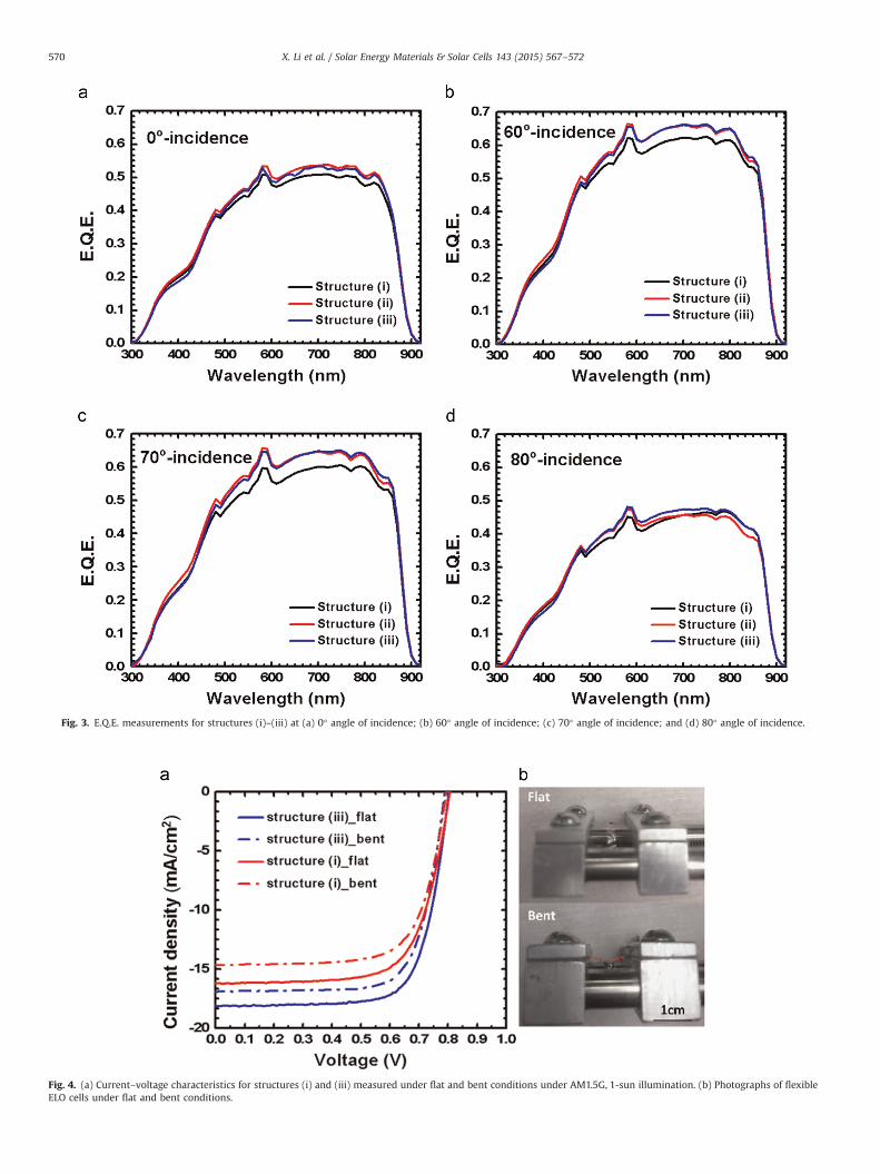
Fig. 3a–d shows measured external quantum efficiency (E.Q.E.)for structures (i)–(iii), at incident angles of 0°, 60°, 70°, and 80°, inwhich the change in total illumination incident on the cell area ateach incident angle is taken into account, so that E.Q.E. is calcu-lated assuming that the incident light intensity does not changewith varying the incident angle. In creating the Al2O3 nanoislandstructures on devices studied in this set of measurements, weperformed fabrication process steps essentially the same as thoseshown in Fig. 1e–g but with PS nanospheres 750 nm rather than1000 nm in diameter, and subsequent deposition of 375 nm ofAl2O3 rather than 500 nm. Based on numerical calculation resultsreported in our earlier work [19], it is found that for the Al2O3
nanoisland structure, the optimal photovoltaic performance isachieved with nanosphere diameters D2 greater than 500 nm, and
Photograph of ELO GaAs solar cell integrated with flexible PET packaging sheet.. (d) Calculated ratio for Jsc of integrated structure (iii) over that of structures (i) and
Fig. 3. E.Q.E. measurements for structures (i)–(iii) at (a) 0° angle of incidence; (b) 60° angle of incidence; (c) 70° angle of incidence; and (d) 80° angle of incidence.
Fig. 4. (a) Current–voltage characteristics for structures (i) and (iii) measured under flat and bent conditions under AM1.5G, 1-sun illumination. (b) Photographs of flexibleELO cells under flat and bent conditions.
X. Li et al. / Solar Energy Materials & Solar Cells 143 (2015) 567–572570
Fig. 5. Photographs of a water droplet on (a) moth-eye textured PET packaging sheet, and (b) planar PET packaging sheet, along with the contact angles measured for each.
X. Li et al. / Solar Energy Materials & Solar Cells 143 (2015) 567–572 571
the photovoltaic performance differs very little for different valuesof D24500 nm.
Compared to structure (i) without optical nanostructures,structure (ii) shows overall improved antireflection performanceover the entire range of incident angles, due to the reduced Fresnelreflection at the air/PET interface via the moth-eye texturedstructure. Note that at 80° angle of incidence, structure (ii) showsslightly decreased E.Q.E. compared to structure (i) for wavelengthsgreater than 740 nm, which we attribute to fabrication imperfec-tions. Compared to structure (ii), structure (iii) shows very similarantireflection performance at incident angles of 0°, 60°, and 70°,and further improved antireflection performance at 80° angle ofincidence, which demonstrates the effectiveness of our approachin improving flexible ELO cell efficiency over a broad range ofincident angles.
Fig. 4a shows measured current–voltage characteristics forstructures (i) and (iii) under AM1.5G, 1-sun illumination, underboth flat and bent conditions. Flexible ELO cells were bent, using ahome-made clipping apparatus, to a radius of curvature of 2.9 cm,as shown in Fig. 4b. Structure (i) yields a Jsc of 16.20 mA/cm2 whenflat, and 14.63 mA/cm2 when bent, which is a 9.7% decrease in Jscfrom flat to bent condition. On the other hand, the structure (iii)yields a Jsc of 18.14 mA/cm2 at flat condition, and 16.92 mA/cm2 atbent condition, which is a 6.7% decrease in Jsc from flat to bentcondition, smaller than that for structure (i) without opticalnanostructures. In the computation of Jsc for each measurement,we divide the measured total current by the original cell area. Theimproved Jsc of structure (iii) under bent condition is attributed tothe substantially improved transmission for TE polarized compo-nent of the incident light at larger incident angles [19]. The slightlyreduced Voc values for structures (i) and (iii) are due to thereduction in photocurrent density under bent condition.
In real photovoltaic applications, cell efficiency also tends todegrade with the accumulation of dust and other contaminants onthe cell surface [21–24], which reduces the optical absorptionefficiency. Various approaches have been studied to overcome thisproblem, including utilizing the hydrophobic characteristics ofbiomimetic surfaces [25–27]. Our moth-eye textured PET packa-ging sheet surface has hydrophobic properties comparable tothose reported previously [28,29]. Photographs of a water dropleton a piece of moth-eye textured PET packaging sheet and unpat-terned planar PET packaging sheet are shown in Fig. 5a and b,respectively. The water droplet on moth-eye textured PET packa-ging sheet has a contact angle �130° with respect to the sheetsurface, significantly larger than that of the unpatterned planarPET sheet, which has a contact angle of �64°. This observationsuggests that in addition to the superior broadband, omnidirec-tional antireflection performance, self-cleaning behavior isanother desirable attribute of the moth-eye textured PET packa-ging sheet.
4. Conclusion
In summary, we have demonstrated a highly effective antire-flection strategy that can be readily implemented for flexible ELOGaAs solar cells, and that is able to substantially boost cell effi-ciency over broad ranges of incident angles and wavelengths. ELOGaAs solar cells fully integrated with moth-eye textured PETpackaging sheet and Al2O3 nanoisland array structure are observedto yield 9% increase in Jsc at normal incidence, and up to 52%increase in Jsc at 80° angle of incidence, compared to referencecells without the Al2O3 nanoisland structure combined withunpatterned PET packaging sheet. Current–voltage measurementsshow that the ELO cell fully integrated with optical nanostructuresyields both higher absolute Jsc value (18.14 mA/cm2) at flat condi-tion, and less reduced Jsc when it is bent (6.7% reduction in Jsc),compared to those of the reference cell without optical nanos-tructures (16.20 mA/cm2, 9.7% reduction in Jsc when bent). More-over, superior self-cleaning properties of moth-eye textured PETpackaging sheet are demonstrated. With more advanced fabrica-tion techniques, such as roll-to-roll nanoimprint lithography [30–33], we anticipate that such approach can be employed for cellswith much larger areas that are required for various photovoltaicapplications.
Acknowledgments
Part of this work was supported by the U.S. Army ResearchLaboratory, the National Science Foundation (ECCS-1120832 andDMR-1311866), and the Judson S. Swearingen Regents Chair inEngineering at the University of Texas at Austin.
References
[1] M. Konagai, M. Sugimoto, K. Takahashi, High efficiency GaAs thin film solarcells by peeled off technology, J. Cryst. Growth 45 (1978) 277–280.
[2] R. Tatavarti, A. Wibowo, G. Martin, F. Tuminello, C. Youtsey, G. Hiller, N. Pan, M.W. Wanlass, M. Romero, InGaP/GaAs/InGaAs inverted metamorphic (IMM)solar cells on 4″ epitaxial lifted off (ELO) wafers, in: Proceedings of the 35thIEEE PVSC Conference, 2010, pp. 002125–002128.
[3] J.J. Schermer, G.J. Bauhuis, P. Mulder, W.J. Meulemeesters, E. Haverkamp, M.M.A.J. Voncken, P.K. Larsen, High rate epitaxial lift-off of InGaP films from GaAssubstrates, Appl. Phys. Lett. 76 (2000) 2131.
[4] G.J. Bauhuis, P. Mulder, E.J. Haverkamp, J.C.C.M. Huijben, J.J. Schermer, 26.1%thin-film GaAs solar cells using epitaxial lift-off, Sol. Energy Mater. Sol. Cells 9(2009) 1488–1491.
[5] K. Lee, J.D. Zimmerman, X. Xiao, K. Sun, S.R. Forrest, Reuse of GaAs substratesfor epitaxial lift-off by employing protection layers, J. Appl. Phys. 111 (2012)033527.
[6] K.M. Trautz, P.P. Jenkins, R.J. Walters, D. Scheiman, R. Hoheisel, R. Tatavarti,R. Chan, H. Miyamoto, J.G.J. Adams, V.C. Elarde, J. Grimsley, Mobile solarpower, IEEE J. Photovolt. 3 (1) (2013) 535–541.
[7] N. Pan, Epitaxial lift-off of large-area GaAs multi-junction solar cells for highefficiency clean and portable energy power generation, in: Proceedings of the
[12] K. Choi, S.H. Park, Y.M. Song, Y.T. Lee, C.K. Hwangbo, H. Yang, H.S. Lee, Nano-tailoring the surface structure for the monolithic high-performance antire-flection polymer film, Adv. Mater. 22 (2010) 3713–3718.
[13] K.C. Park, H.J. Choi, C.H. Chang, R.E. Cohen, G.H. McKinley, G. Barbastathis,Nanotextured silica surfaces with robust superhydrophobicity and omnidir-ectional broadband supertransmissivity, ACS Nano 6 (2012) 3789–3799.
[14] N. Yamada, T. Ijiro, E. Okamoto, K. Hayashi, H. Masuda, Characterization ofantireflection moth-eye film on crystalline silicon photovoltaic module, Opt.Express 19 (2011) A118–A125.
[15] S. Chhajed, M.F. Schubert, J.K. Kim, E.F. Schubert, Nanostructured multilayergraded-index antireflection coating for Si solar cells with broadband andomnidirectional characteristics, Appl. Phys. Lett. 93 (2008) 251108.
[16] J. Rybczynski, U. Ebels, M. Giersig, Large-scale, 2D arrays of magnetic nano-particles, Colloids Surf. A: Physicochem. Eng. Asp. 219 (2003) 1–6.
[17] X.H. Li, P. –C. Li, D.Z. Hu, D.M. Schaadt, E.T. Yu, Light trapping in thin-film solarcells via scattering by nanostructured antireflection coatings, J. Appl. Phys. 114(2013) 044310.
[18] X.H. Li, P. –C. Li, D.Z. Hu, D.M. Schaadt, E.T. Yu, Angular dependence of lighttrapping in In0.3Ga0.7As/GaAs quantum-well solar cells, J. Appl. Phys. 115(2014) 044303.
[19] X.H. Li, P. –C. Li, L. Ji, C. Stender, C. McPheeters, S.R. Tatavarti, K. Sablon, E.T. Yu,Subwavelength nanostructures integrated with polymer-packaged III/V solarcells for omnidirectional, broad-spectrum improvement of photovoltaic per-formance, Prog. Photovolt.: Res. Appl. (2014), http://dx.doi.org/10.1002/pip.2565.
[20] P. –C. Li, E.T. Yu, Large-area omnidirectional coating on low-index materials, J.Opt. Soc. Am. B 30 (2013) 2584–2588.
[21] J. Zhu, C.M. Hsu, Z.F. Yu, S. Fan, Y. Cui, Nanodome solar cells with efficient lightmanagement and self-cleaning, Nano Lett. 10 (6) (2010) 1979–1984.
[22] Y.B. Park, H. Im, M. Im, Y.K. Choi, Self-cleaning effect of highly water-repellentmicroshell structures for solar cells, J. Mater. Chem. 21 (2011) 633–636.
[23] L.K. Verma, M. Sakhuja, J. Son, A.J. Danner, H. Yang, H.C. Zeng, C.S. Bhatia, Self-cleaning and antireflective packaging glass for solar modules, Renew. Energy36 (9) (2011) 2489–2493.
[24] W.L. Min, B. Jiang, P. Jiang, Bioinspired self-cleaning antireflection coatings,Adv. Mater. 20 (2008) 3914–3918.
[25] S.A. Boden, D.M. Bagnall, Tunable reflection minima of nanostructured anti-reflective surfaces, Appl. Phys. Lett. 93 (2008) 133108.
[26] C. Chen, G. Hubbard, P.A. Shields, C. Liu, D.W.E. Allsopp, W.N. Wang, S. Abbott,Broadband moth-eye antireflection coatings fabricated by low-cost nanoim-printing, Appl. Phys. Lett. 94 (2009) 263118.
[27] J.H. Shin, K.S. Han, H. Lee, Anti-reflection and hydrophobic characteristics ofM-PDMS based moth-eye nano-patterns on protection glass of photovoltaicsystems, Prog. Photovolt.: Res. Appl. 19 (2011) 339–344.
[28] S. Nishimoto, B. Bhushan, Bioinspired self-cleaning surfaces with super-hydrophobicity, superoleophobicity, and superhydrophilicity, RSC Adv. 6(2013) 671–690.
[31] M.G. Kang, M.S. Kim, J. Kim, L.J. Guo, Organic solar cells using nanoimprintedmetal electrodes, Adv. Mater. 20 (2008) 4408–4413.
[32] X. Zhang, A. Hosseini, X. Lin, H. Subbaraman, R.T. Chen, Polymer-based hybrid-integrated photonic devices for silicon on-chip modulation and board-leveloptical interconnects, IEEE J. Sel. Top. Quantum Electron. 19 (2013) 196–210.
[33] S. Ahn, J. Cha, H. Myung, S.M. Kim, S. Kang, Continuous ultroviolet rollnanoimprinting process for replicating large-scale nano- and micropatterns,Appl. Phys. Lett. 89 (2006) 213101.