1 Final Manuscript for IEEE Transactions on Advanced Packaging SOLDER-ASSEMBLED LARGE MEMS FLAPS FOR FLUID MIXING Zhichun Ma 1* , Elizabeth Bradley 1 , Thomas Peacock 2 , Jean R. Hertzberg 1 , and Yung-Cheng Lee 1 1 University of Colorado, Boulder, CO 80309-0427 2 Massachusetts Institute of Technology, Cambridge, MA 02139 ABSTRACT We describe surface-micromachined thermal actuator-based MEMS flaps with a length scale of 1,000 μm. These flaps were developed for the enhancement of fluid mixing in an experimental study of a planar air jet. The scales of the flow physics required the actuators to be much larger than the typical MEMS scales, and the experiment required an array of 10 flaps (1 cm in length) to be soldered onto a ceramic substrate with high precision. These unusual requirements made it difficult to achieve good assembly yields that could provide large deflections. To improve the yields and deflections, we modified the initial flap design by reducing the size of the solder pads, removing sharp corners, changing the number and the width of the actuator’s hot arms, and strengthening the support beams. In addition, we developed a controllable assembly process to reflow tin/lead solder on gold pads, and we used numerical simulations extensively in the design process to improve the performance. The experimental measurements corroborated these simulations: the deflection was increased from 6.4 to 11.1 μm under a 5 V applied voltage. Flow velocity measurements showed that these MEMS flaps amplified the natural instabilities of the planar jet. * Zhichun Ma; Department of Mechanical Engineering Campus Box 0427, University of Colorado, Boulder, CO 80309-0427 Phone: (720) 329-4585; FAX: (303) 492-3498; E-mail: [email protected]
Transcript
1
Final Manuscript for IEEE Transactions on Advanced Packaging
SOLDER-ASSEMBLED LARGE MEMS FLAPS FOR FLUID MIXING
Zhichun Ma1*, Elizabeth Bradley1, Thomas Peacock2, Jean R. Hertzberg1, and Yung-Cheng Lee1
1University of Colorado, Boulder, CO 80309-0427
2Massachusetts Institute of Technology, Cambridge, MA 02139
ABSTRACT
We describe surface-micromachined thermal actuator-based MEMS flaps with a length scale of 1,000
µm. These flaps were developed for the enhancement of fluid mixing in an experimental study of a
planar air jet. The scales of the flow physics required the actuators to be much larger than the typical
MEMS scales, and the experiment required an array of 10 flaps (1 cm in length) to be soldered onto a
ceramic substrate with high precision. These unusual requirements made it difficult to achieve good
assembly yields that could provide large deflections. To improve the yields and deflections, we modified
the initial flap design by reducing the size of the solder pads, removing sharp corners, changing the
number and the width of the actuator’s hot arms, and strengthening the support beams. In addition, we
developed a controllable assembly process to reflow tin/lead solder on gold pads, and we used numerical
simulations extensively in the design process to improve the performance. The experimental
measurements corroborated these simulations: the deflection was increased from 6.4 to 11.1 µm under a
5 V applied voltage. Flow velocity measurements showed that these MEMS flaps amplified the natural
instabilities of the planar jet.
*Zhichun Ma; Department of Mechanical Engineering Campus Box 0427, University of Colorado, Boulder, CO 80309-0427 Phone: (720) 329-4585; FAX: (303) 492-3498; E-mail: [email protected]
2
Index Terms: MEMS, actuator, solder, flip-chip, packaging, modeling, flow control.
I. INTRODUCTION
The accurate prediction and control of fluid flows have long been major research areas. The ability
to control flow, particularly in aerospace and combustion applications, can bring significant economic
and environmental benefits. Most experimental flow-control studies have been performed using
conventionally machined actuators [1-3], but there has been strong interest in using MEMS based
technology for flow control because it offers several advantages over conventional machining, such as
batch processing of devices on the µm scale. A review of the use of MEMS devices for flow control is
given by Ho and Tai [4]. Many different geometries have been evaluated for flow applications, including
micro fans and various types of flaps [5-8].
Most studies on MEMS/fluids interactions have to date focused on the MEMS actuator’s effects on
the fluid flow [7-8]. To the best of our knowledge, there are not many studies that address the design and
fabrication of MEMS specifically for the purpose of fluid mixing. In this paper, we describe the design,
fabrication, assembly, and testing of thermal-actuator based MEMS flaps for the purpose of forcing a
planar jet of air. A schematic of the experiment is presented in Figure 1. The MEMS flaps are mounted
on either side of the jet along the exit slit, providing a disturbance that is naturally amplified as it travels
downstream. The planar jet is unstable when the Reynolds number, based on the half-width and peak
velocity of the jet, exceeds a critical value [9]. Small-scale velocity disturbances in the boundary layer
are amplified as they progress downstream, generating coherent structures that dominate the flow field.
The anti-symmetric instability has been excited using acoustic forcing [10].
Using MEMS micro-actuators, we have been able to selectively excite both the anti-symmetric and
the symmetric instabilities of the planar jet at low Reynolds numbers [11]. In addition, an asymmetric
3
mode in which only one side of the jet is forced has been studied [11]. This was possible because the
micro-actuators allowed us to provide localized disturbances, with an arbitrary phase relationship, on
either side of the experimental jet. This is contrast to acoustic techniques, for which the entire flow is
subject to forcing of uniform phase.
The effect of the micro-actuators is significant, as shown by the images in Figure 2. In the unforced
jet, Figure 2(a), the MEMS flaps are motionless, the flow is laminar, and there is little entrainment of the
surrounding air into the jet. In Figure 2(b), we show an image of the same jet, subject to asymmetric
forcing at 6Hz by MEMS flaps. The instability excited by the flaps gives rise to large-scale vortices.
These vortices provide enhanced mixing of the jet with the ambient air. This phenomenon is known to
have a profound effect on combustion processes. In order to investigate the effect of different forms of
forcing on the nonlinear development of the flow, it is very important to study the design and fabrication
of MEMS flaps in depth.
The driving mechanism for the flaps was electro-thermal. This technology is supported by current
commercial foundry processes and provides enough deflection and force to disturb the flow [15]. The
polysilicon flaps were mounted on a ceramic substrate using a flip-chip solder assembly technique. This
assembly approach allowed multiple actuators to be accurately positioned on a ceramic substrate, as the
solder surface tension aligns the flaps on the substrate during the solder re-flow process. The flap
assembly was then mounted next to the exit of the jet.
The initial design for the MEMS flaps is shown in Figure 3. Views are referenced by the final
assembly position. The deflection of the flap was upward. These actuators were intended for a feasibility
study, which was highly successful in demonstrating the ability to influence a jet flow. Improvements
were needed, however, as the original design was far too fragile and inefficient to survive laboratory
conditions. Moreover, experimental study of the planar jet required a 1 cm-long array of flaps to be
4
mounted along the edge of the jet. As each MEMS flap was 1mm long, this required mounting 10 flaps
in close proximity on a ceramic substrate, with very high precision (see Figure 4). Such an assembly is
two orders of magnitude larger than a typical MEMS device, providing a significant challenge for
fabrication. In addition, the flaps must be uniformly aligned on the substrate, so as to provide a uniform
disturbance to the jet. This requirement, plus efficiency requirements, demanded major advances in the
MEMS flap technology. Significant efforts in design, simulation, characterization, fabrication, and
assembly were needed. We describe our solutions to these challenges in the following sections.
In section II, we present a new design of the MEMS actuators, and describe structural changes that
we made to the original design in order to improve performance. Then, in section III, we discuss the
design process and detailed numerical simulations. Next, in section IV, we describe the assembly process
that was refined to enable consistent fabrication of the actuators. Finally, in section V, we present
experimental results on the performance of the devices, showing good agreement with the predictions of
the numerical simulations. We close with novel experimental flow mixing results that were attained
with these improved MEMS flap assemblies.
II. DESIGN
The first generation of MEMS flaps, shown in Figure 3, worked well for initial feasibility
demonstrations, but they had several problems:
1. Incomplete release: it took more than twelve minutes to remove the oxide layer under the solder pad
for each flap, and it was difficult to control such a long process for complete release.
2. Broken hot arms: the hot arms were weak and easily broken during assembly or operation.
3. Small movements and flimsy structure: the flap's vertical movement was small and strongly affected
by the moving support arms.
5
The release problem was solved by using multiple bonding pads. The single large solder pad shown
in the original design (Figure 3) was replaced by two pads, as shown in Figure 5. Between the pads, etch
holes were added to enhance the release process.
The difficulties with the hot arms were solved by decreasing the number of arms, while increasing
their width. As shown in Figures 5 and 6, the hot-arm width was increased from 5 to 12 µm, and the
number of arms for each flap was reduced from 21 to 7. The intention here was to increase the total
electrical resistance of the hot arms on each flap. Furthermore, the first-generation MEMS flaps had
sharp corners on each arm near the edge of support beams and flap plate, which was structurally
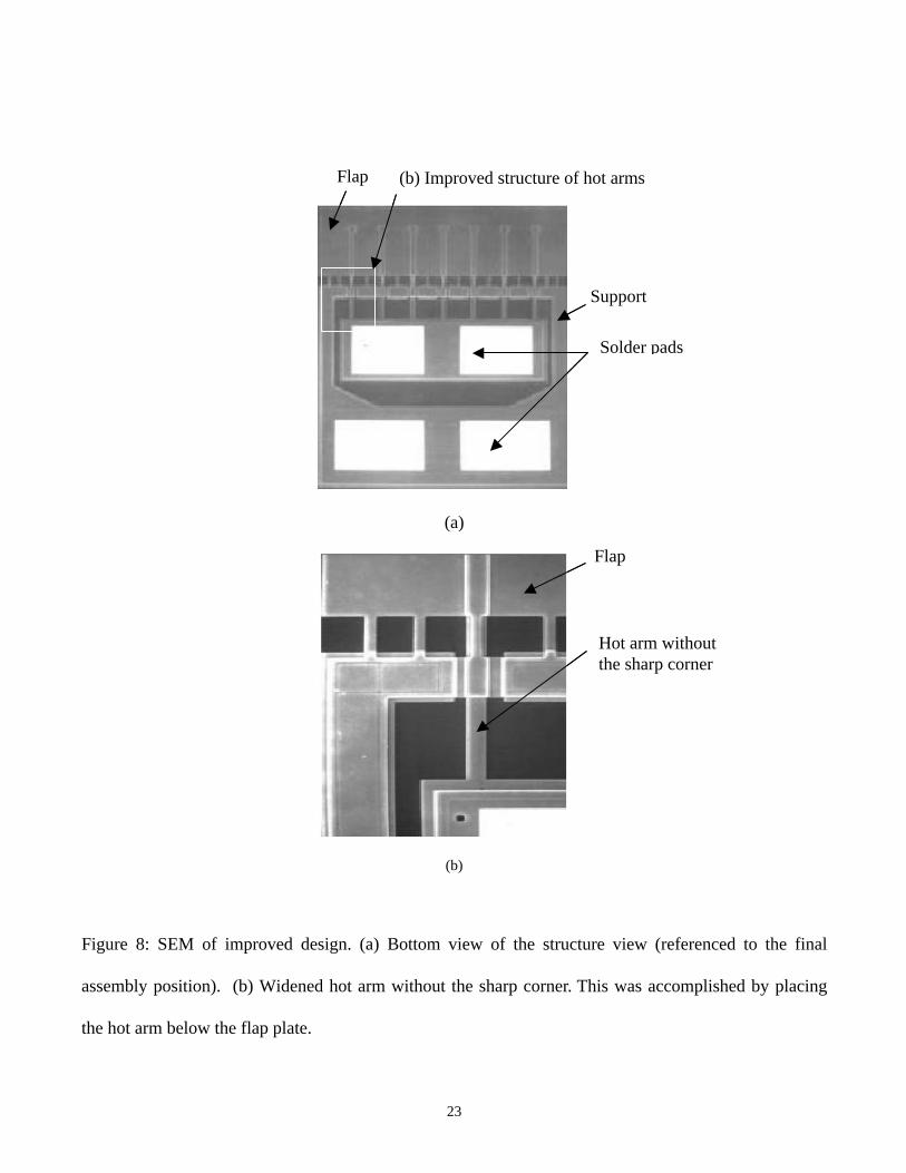
unsound (see Figure 7). By placing the hot arms below, when viewed from bottom (referenced by the
final assembly position), the support beams and attaching them at the bottom of the flap plate, these
corners were eliminated, as shown in Figure 8, and the flap deflection was now downward.
The movement problem was solved by strengthening the support beams and shortening the hot arms.
As shown in Figure 3, each support beam in the original design was 420 µm long and 45 µm wide. This
was too long and compliant. By adding a triangular corner plate and increasing the beam width from 45
to 55 µm, we enhanced the stiffness in the vertical direction significantly. The tip of the hot arm was
moved inward from the edge of the flap by 75 µm, allowing the hot arms to push the flap much further
downward, as the flap deflection beyond the tip of the hot arm was proportional to the slope of the
deformation.
Although these design changes appear to eliminate the problems with the first-generation design, it is
impossible to verify that conjecture a priori. For example, even with the same current density, the
widened hot arm might not generate the same bending power because the structure could have different
temperature distributions resulting from different heat transfer characteristics. Such nonlinear
6
interactions cannot be analyzed easily, and so we used numerical simulation tools to simulate the
behavior of the actuator in order to characterize the new design prior to fabrication.
III. SIMULATION
Commercial software, CoventorWare [13], was used to perform numerical simulations of the actuator
designs shown in Figures 9-14. CoventorWare uses the finite element approach, incorporating electro-
thermal-mechanical analysis. Brick elements of 27 nodes with dimensions 80µm x 80µm x 10µm were
used in the simulation. CoventorWare uses an iterative process to calculate the static deflection of the
actuator. The voltage-current distribution was solved first, followed by a heat-transfer analysis. The
resulting temperature field was used to determine the mechanical deflection. The thermal and
mechanical solutions were fed back into the electrical modeling module of the software to correct for
temperature effects. This iterative process continued until the solutions converged to within 0.1%
tolerance.
The simulation results are presented in Figures 9-14. The boundary conditions were as follows:
1) The regions in contact with the solder pads and the supporting arms at the side were assumed to be
rigid, and were therefore neglected in the simulation.
2) The ends of the hot arms and the flexures supporting the flap were assumed to be fixed, and were
maintained at room temperature.
3) A known driving voltage (e.g., 5 V) was applied across the hot arms and the support flexures.
4) Convective and radiation heat transfer occurred from all surfaces that were in direct contact with the
surrounding air.
7
5) Between the hot arms and the flap there was a small air gap of about 0.75µm. The air conduction
across this gap was significant, and was modeled as convective to avoid mesh difficulties, with a
coefficient derived as 5.2x10⁴ w/m2k from equation (1):
kmwmkmw
dKh air ⋅×=
×⋅
== −24
6 /102.51075.0/039.0
(1)
Where Kair is thermal conductivity of air, and d is the gap width.
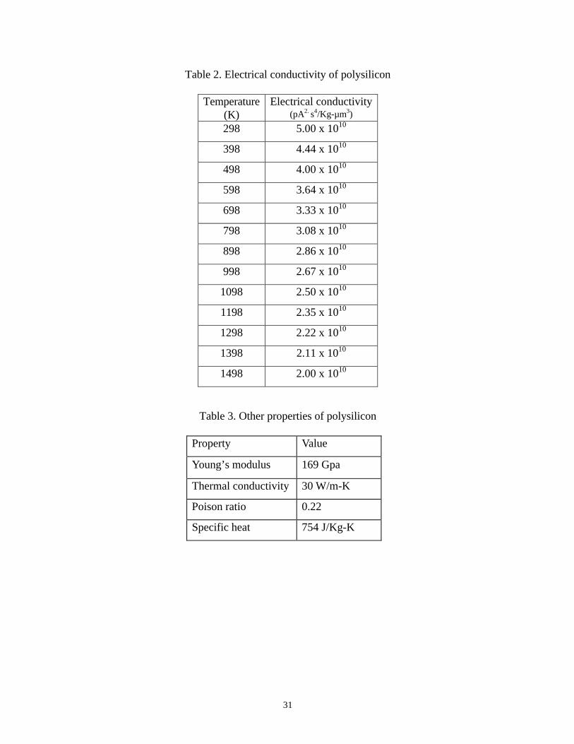
The material properties used in the simulation were those of polysilicon. Among these, the most
important was the value of electrical conductivity, given by Butler [14], as this was affected by the
application of electric currents that generated heat. The temperature-dependent electrical properties of
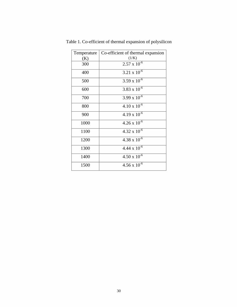
polysilicon used in the simulation are listed in Table 1-3, along with some of the other physical
properties [15-18].
The simulation results obtained were very encouraging. Figures 9 and 10 show the comparison of the
temperature distributions between the old and the new flap designs. The maximum temperature and the
length of the high-temperature regions achieved in the hot arms remained approximately unchanged.
Such temperature distributions indicate that the widened hot arms had similar thermal expansions as in
the first-generation flap designs. This verified the design choice to reduce the number of hot arms.
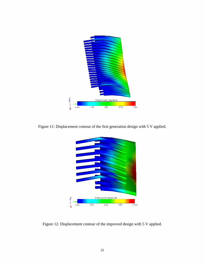
With thermal expansions similar to those described in the previous paragraph, the maximum tip
deflection was improved from 6.4 to 11.1 µm with 5V applied (see Figures 11 and 12). As shown in
Figure 12, the flap region beyond the tips of the hot arms in the new design extended the deflection
about 5 µm, which is the difference between the displacements of 11 and 6 µm. In addition to the large
deflection, the distribution of the deflection became more uniform along the length of the flap, varying
by 0.3 µm.
8
In contrast, the displacements shown in Figure 11 are non-uniform, with large deflections occurring
in the center region of the flap. This warped deflection pattern was the result of the pulling forces from
the hot arms. Such non-uniformity was reduced by moving the tips away from the edge of the flap and
changing the distribution of the pushing forces from the hot arms. With the new design, a large portion
of the deflection was related to the angle at the flap tip, rather than the displacements of that tip.
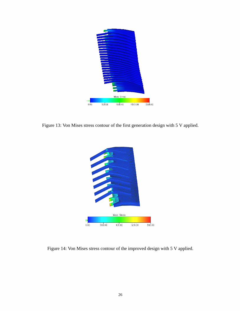
Another concern is the fragility of the MEMS assembly. As shown in Figures 13 and 14, with
enlarged cross-sectional area of the hot arms, the maximum von Mises stress of the improved design was
only 500 Mpa. This was much smaller than 2000 Mpa of the previous design. Maximum stress occurred
at the junction between the solder pads and the support flexures. Because stress solutions were mesh-
dependent, we used the same mesh sizes in both simulations in order to make the comparison
reasonable. The new design reduced the stresses significantly, which translates to improved reliability
and durability.
Given these encouraging numerical simulation results, we submitted the new design for fabrication
using the commercial MUMPS process [19], and then assembled them for further characterization and
experimental measurements.
IV. ASSEMBLY
Figure 15 shows the schematic diagram and an SEM image of one of the solder-assembled MEMS
flaps from Figure 4. The fabrication and assembly processes were similar to the flip-chip processes
reported in previous studies [20], with one major difference: the solder joints, with a pad size of 320 µm
x 200 µm, were much larger than in any previous study. As a result, a special technique had to be
developed to solder a large size MEMS flap onto the ceramic substrate.
9
The MUMPS devices came with gold pads after fabrication. Indium or indium/lead solder alloys
were evaluated first due to their compatibility with gold pads, but their re-flow properties were very poor
because of gold-indiumide formation associated with high gold-contents. For effective re-flow,
63Sn/37Pb soldering was chosen. However, Sn/Pb solder has the well-known gold scavenge effect. This
effect was managed through a controlled procedure listed below:
A. Before flip-chip bonding
1. Clean the ceramic substrate using acetone and methanol. Then put the substrate in argon plasma
cleaner for 5 minutes at 25 W.
2. Place ceramic substrate on heating stage at room temperature.
3. Use micro-positioning probes to position solder balls on gold electrode pattern etched onto the
ceramic substrate.
4. Enclose the heating stage and pass N2 over the substrate.
5. Commence heating to 193 degrees centigrade.
6. Introduce formic acid vapor to the N2 when the temperature reaches 160 degrees centigrade.
7. At 183 degrees centigrade the solder balls begin to melt, wetting the electrodes. Turn off both the
heating element and the formic acid vapor, and increase the flow of N2.
8. Wait for the substrate to reach room temperature before removing the ceramic substrate from the
heating chamber.
B. After flip-chip bonding
9. Place the assembly in argon plasma cleaner for 5 minutes at 25 W.
10. Repeat steps 2 to 6.
10
11. When the temperature reaches 183 degrees centigrade, turn off the formic acid vapor, leave for 3
minutes, then increase the nitrogen flow rate and turn off the heating element.
12. When the substrate is at room temperature, turn off the N2 and remove the substrate from the heating
chamber.
V. CHARACTERIZATION
The performance of the assembled MEMS flaps was investigated using a ZYGO interferometer
microscope that is capable of measuring vertical deflections of the flaps. For comparison, the measured
and simulated deflections of the MEMS flap are presented in graphical form in Figure 16 (a). The
deflection increased from approximately 0.5 µm to 12 µm as the voltage was increased from 1 to 5 volts.
The agreement between experiment and simulation is excellent, confirming both the accuracy of the
model and the effectiveness of the design: the amplitude of deflection as a function of voltage is
significantly improved over the first-generation MEMS flaps. This new design for the electro-thermal
MEMS actuators is more than capable of providing the required disturbance for the jet flow experiment.
The dynamic behavior of the MEMS flaps is presented in Figure 16 (b). This was obtained by reflecting
a HeNe laser beam bounced off the free end of a vibrating flap and tracking the displacement of the
reflected beam. The resonant frequency of a flap is around 25 Hz, as shown in Figure 16 (b). Above this
value, the amplitude of oscillation decreased significantly with increasing frequency to a value of about
4 µm at 200 Hz.
Using these improved MEMS flaps, we have been able to selectively excite the natural instabilities of
the planar air jet. As illustrated in Figure 1(b), filtered air entered the base of a plenum, whose internal
cross-section was 400mm by 15mm, and passed through three flow treatment screens constructed using
11
24 mesh with 0.19 mm diameter wire. Upon reaching the top, the air entered a matched cubic
contraction of area ratio 6 to 1, to further reduce turbulence and produce a more uniform flow. Flow
emerged from an exit slit 400mm long and 2.5±0.01mm wide. The system was highly sensitive to
mechanical vibrations and motion of the ambient air. To minimize these effects, the entire experiment
stood on vibration control mounts and was semi-enclosed by a 1m3 plexiglas box. External forcing of
the jet was provided by arrays of the MEMS flap assembly described in the previous sections, positioned
on either side of the exit slit.
A TSI 1210 hotwire probe and a TSI 1010 hotwire anemometer were used to measure the velocity
profile and velocity fluctuations in the jet. The probe was mounted on translation stages and could be
moved in the streamwise and cross-stream directions with an accuracy of 0.025mm. The hotwire was
operated by a constant temperature method, and its output digitized using a 12-bit A/D converter. First,
the centerline velocity was measured along the length of the exit slit, and was found to be uniform to
within 2%, supporting our assumption of a 2D flow near the exit slit. Thereafter, hotwire measurements
of both mean and fluctuating velocity profiles were acquired across the center of the exit slit. Compare
to the unforced flow, the amplitudes of disturbances forced by the MEMS flaps can be 7~50 times their
natural levels. Figure 17 compares the forced (17b) and unforced flow (17a), clearly showing the effects
of these improved flaps.
VI. CONCLUSIONS
The first-generation actuators developed for a feasibility study of MEMS-based flow control had
three major problems: incomplete release, broken hot arms, and small deflections. To improve on these
flaps, we have reduced the size of solder pads, removed sharp corners, changed the number and the
width of the actuator’s hot arms, and strengthened the support beams. In addition, we have developed a
12
controllable process to re-flow tin/lead solder on gold pads. Numerical simulations using CoventorWare
were used to characterize the performance of the new design prior to fabrication. Simulation results
indicated that the new design increased flap-tip deflection from 6.5 to 11.1 µm for a 5 V driving voltage,
and reduced the maximum von Mises stress from 2000 to 500 Mpa. The simulated deflection-.vs.-
voltage relationship has been confirmed by experimental characterizations. Experimental results show
that forcing the instabilities of the planar jet with these flaps increases the amplitudes of those
instabilities by a factor of 7~50. Ongoing studies include the details of flow around the flaps, and the
development of the instabilities in the jet.
Acknowledgments
This work is supported by the National Science Foundation with award number ACI-0083004. The
authors would like to express their appreciation for the support of Coventor, Inc., and helpful
discussions with W. Zhang, P. Kladitis, K. Harsh, J. Negretti, and J. P. Giardino at the University of
Colorado.
References
[1] J. M. Wiltse and A. Glezer, “Manipulation of free shear flows using piezoelectric actuators”, J. Fluid
Mech., vol. 249, pp. 261-285, 1993.
[2] J. M. Wiltse and A. Glezer, “Vectoring and small-scale motions in free shear flows”, Phys. Fluids,
vol.10, pp. 2026-2036, 1998.
[3] S. A. Jacobson, and W. C. Reynolds, “Active control of stream wise vortices and steaks in boundary
layers”, J. Fluid Mech., vol. 360, pp. 179-211, 1998.
13
[4] C-M. Ho, and Y-C. Tai, “Micro-electro-mechanical-systems (MEMS) and fluid flows”, Ann. Rev.
Fluid Mech., vol. 30, pp. 579-612, 1998.
[5] Z. Ma, T. Peacock, E. Bradley, and Y-C. Lee, “Solder-assembled MEMS flaps to enhance fluid
mixing”, in Proc. of ASME IMECE (International Mechanical Engineering Congress and
Exposition), 2001, pp. 731-737.
[6] T. Tsao, C. Liu, Y-C. Tai, and C-M. Ho, “Micromachined magnetic actuators for active fluid
control”, Application of Microfabrication to Fluid Mechanics, ASME, vol. 197, pp. 31-38,1994.
[7] L. Löfdahl, and M. Gad-el-Hak, “MEMS applications in turbulence and flow control”, Prog. Aero.
Sci., vol. 35, pp. 101-203, 1999.
[8] R. Linderman, “Development and parametric analysis of the resonant micro fan for fluidic transport
and suspended particle collection”, Ph.D. dissertation, University of Colorado, 2002.
[9] E. N. da C. Andrade, “The velocity distribution in a liquid-into-liquid jet. Part 2: The plane jet”, in
Proc. Phys. Soc., 1939, pp. 784-789.
[10] G. B. Brown, “On vortex motion in gaseous jets and the origin of their sensitivity to sound”, in
Proc. Phys. Soc., 1935, pp. 703-707.
[11] T. Peacock, E. Bradley, J. Hertzberg, and Y. C. Lee, “Forcing a planar jet flow using MEMS”,
Phys. Fluids, to be published.
[12] W. Cowan and V. M. Bright, “Vertical thermal actuators for micro-opto-electro-mechanical
systems”, in Proc. SPIE, 1997, vol. 3226, pp. 137-146.