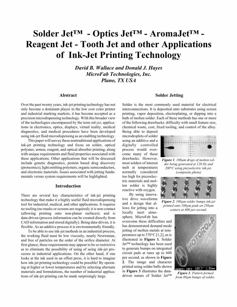
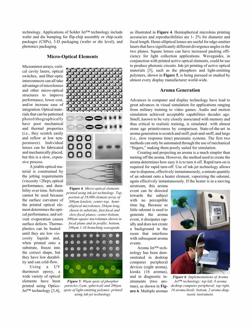
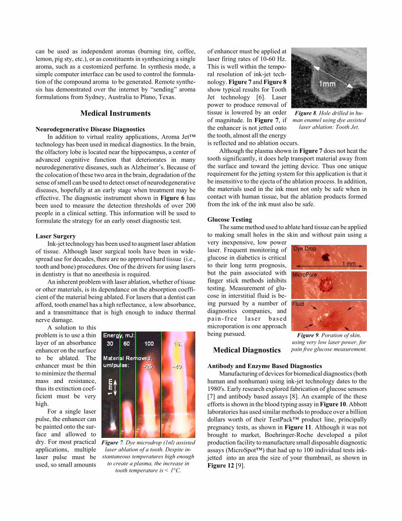
Figure 1. 100μm drops of molten sol- der being generated at 120 Hz and 200°C using piezoelectric ink-jet. (composite photo) Figure 3: Pattern formed from 80μm bumps of solder. Figure 2. 100μm solder bumps ink-jet printed onto 100μm pads on 250μm centers at 400 per second. Solder Jet™ - Optics Jet™ - AromaJet™ - Reagent Jet - Tooth Jet and other Applications of Ink-Jet Printing Technology David B. Wallace and Donald J. Hayes MicroFab Technologies, Inc. Plano, TX USA Abstract Over the past twenty years, ink-jet printing technology has not only become a dominant player in the low cost color printer and industrial marking markets, it has become accepted as a precision microdispensing technology. With this broader view of the technologies encompassed by the term ink-jet, applica- tions in electronics, optics, displays, virtual reality, medical diagnostics, and medical procedures have been developed using ink-jet fluid microdispensing as an enabling technology. This paper will survey these nontraditional applications of ink-jet printing technology and focus on solder, optical polymer, armoa, reagent, and optical absorber printing, along with unique requirements and fluid properties associated with these applications. Other applications that will be discussed include genetic diagnostics, protein based drug discovery (proteomics), light emitting polymers, organic semiconductors, and electronic materials. Issues associated with jetting funda- mentals versus system requirements will be highlighted. Introduction There are several key characteristics of ink-jet printing technology that make it a highly useful fluid microdispensing tool for industrial, medical, and other applications. It requires no tooling (no masks or screens are required); it is non-contact (allowing printing onto non-planar surfaces); and is data-driven (process information can be created directly from CAD information and stored digitally). Being data-driven, it is flexible. As an additive process it is environmentally friendly. To be able to use ink-jet methods in an industrial process, the working fluid must be low viscosity, nearly Newtonian, and free of particles on the order of the orifice diameter. At first glance, these requirements may appear to be so restrictive as to eliminate the possibility of using of using ink-jet pro- cesses in industrial applications. On the other hand, if one looks at the ink used in an offset press, it is hard to imagine how ink-jet printing technology could be possible! By operat- ing at higher or lower temperatures and by selecting alternate materials and formulations, the number of industrial applica- tions of ink-jet printing can be made surprisingly large. Solder Jetting Solder is the most commonly used material for electrical interconnections. It is deposited onto substrates using screen printing, vapor deposition, electroplating, or dipping into a bath of molten solder. Each of these methods has one or more of the following drawbacks: difficulty with small feature size, chemical waste, cost, fixed tooling, and control of the alloy. Being able to deposit microdroplets of solder using an additive and a digitally controlled process would over- come many of these drawbacks. However, most solders of interest melt at temperatures normally considered too high for piezoelec- tric materials and mol- ten solder is highly reactive with oxygen. By using innova- tive drive waveforms and a design that al- lows for jetting into a locally inert atmo- sphere, MicroFab has overcome these difficulties and has demonstrated demand mode jetting of molten metals at tem- peratures up to 370°C [1,2], as is illustrated in Figure 1. Solder Jet™ technology has been used to generate bumps on integrated circuit pads at rates up to 600 per second, as shown in Figure 2. The image and character printed using solder balls shown in Figure 3 illustrates the data- driven nature of Solder Jet™
Transcript
Figure 1. 100µm drops of molten sol-der being generated at 120 Hz and200°C using piezoelectric ink-jet.
(composite photo)
Figure 3: Pattern formedfrom 80µm bumps of solder.
Solder Jet™ - Optics Jet™ - AromaJet™ -Reagent Jet - Tooth Jet and other Applications
of Ink-Jet Printing TechnologyDavid B. Wallace and Donald J. Hayes
MicroFab Technologies, Inc.Plano, TX USA
Abstract
Over the past twenty years, ink-jet printing technology has notonly become a dominant player in the low cost color printerand industrial marking markets, it has become accepted as aprecision microdispensing technology. With this broader viewof the technologies encompassed by the term ink-jet, applica-tions in electronics, optics, displays, virtual reality, medicaldiagnostics, and medical procedures have been developedusing ink-jet fluid microdispensing as an enabling technology.
This paper will survey these nontraditional applications ofink-jet printing technology and focus on solder, opticalpolymer, armoa, reagent, and optical absorber printing, alongwith unique requirements and fluid properties associated withthese applications. Other applications that will be discussedinclude genetic diagnostics, protein based drug discovery(proteomics), light emitting polymers, organic semiconductors,and electronic materials. Issues associated with jetting funda-mentals versus system requirements will be highlighted.
Introduction
There are several key characteristics of ink-jet printingtechnology that make it a highly useful fluid microdispensingtool for industrial, medical, and other applications. It requiresno tooling (no masks or screens are required); it is non-contact(allowing printing onto non-planar surfaces); and isdata-driven (process information can be created directly fromCAD information and stored digitally). Being data-driven, it isflexible. As an additive process it is environmentally friendly.
To be able to use ink-jet methods in an industrial process,the working fluid must be low viscosity, nearly Newtonian,and free of particles on the order of the orifice diameter. Atfirst glance, these requirements may appear to be so restrictiveas to eliminate the possibility of using of using ink-jet pro-cesses in industrial applications. On the other hand, if onelooks at the ink used in an offset press, it is hard to imaginehow ink-jet printing technology could be possible! By operat-ing at higher or lower temperatures and by selecting alternatematerials and formulations, the number of industrial applica-tions of ink-jet printing can be made surprisingly large.
Solder Jetting
Solder is the most commonly used material for electricalinterconnections. It is deposited onto substrates using screenprinting, vapor deposition, electroplating, or dipping into abath of molten solder. Each of these methods has one or moreof the following drawbacks: difficulty with small feature size,chemical waste, cost, fixed tooling, and control of the alloy.Being able to depositmicrodroplets of solderusing an additive and adigitally controlledprocess would over-come many of thesedrawbacks. However,most solders of interestmelt at temperaturesnormally consideredtoo high for piezoelec-tric materials and mol-ten solder is highlyreactive with oxygen.
By using innova-tive drive waveformsand a design that al-lows for jetting into alocally inert atmo-sphere, MicroFab hasovercome these difficulties andhas demonstrated demand modejetting of molten metals at tem-peratures up to 370°C [1,2], as isillustrated in Figure 1. SolderJet™ technology has been usedto generate bumps on integratedcircuit pads at rates up to 600per second, as shown in Figure2. The image and characterprinted using solder balls shownin Figure 3 illustrates the data-driven nature of Solder Jet™
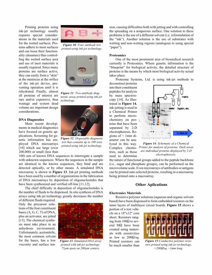
Figure 4. Micro-optical elementsprinted using ink-jet technology. Top,
portion of 19,000 element array of300µm lenslets; center-top, hemi-elliptical microlenses 284µm long,shown in substrate, fast-focal andslow-focal planes; center-bottom,
300µm square microlenses shown infocal plane and in profile; bottom,100µm 1:16 branching waveguide.
Figure 5: 90µm spots of phosphorparticles (1µm, spherical) and 200µmspots of light-emitting polymer, printed
using ink-jet technology.
Figure 6: Implementations of AromaJet™ technology: top left, 8 aroma
technology. Applications of Solder Jet™ technology includewafer and die bumping for flip-chip assembly or chip-scalepackages (CSPs), 3-D packaging (wafer or die level), andphotonics packaging.
Micro-Optical Elements
Micromirror arrays, verti-cal cavity lasers, opticalswitches, and fiber-opticinterconnects can all takeadvantage of microlensesand other micro-opticalstructures to improveperformance, lower cost,and/or increase ease ofintegration. Optical mate-rials that can be patternedphotolithographicallyhave poor mechanicaland thermal properties(i.e., they scratch easilyand reflow at low tem-peratures). Individuallenses can be fabricatedand mechanically placed,but this is a slow, expen-sive process.
A jetable optical ma-terial is constrained bythe jetting requirements(viscosity <20cp), opticalperformance, and dura-bility over time. Solventscannot be used becausethe surface curvature ofthe printed optical ele-ment determines the opti-cal performance, and sol-vent evaporation causessurface defects. Thermo-plastics can be heateduntil they are low vis-cosity liquids and,when printed onto asubstrate, freeze intothe correct shape, butthey have low durabil-ity and can cold-flow.
Using a UVthermoset epoxy, awide variety of opticalelements have beenprinted using Optics-Jet™ technology [3,4],
as illustrated in Figure 4. Hemispherical microlens printingaccuracies and reproducibilities are 1- 2% for diameter andfocal length. Hemi-elliptical lenses are useful for edge-emitterlasers that have significantly different divergence angles in thetwo planes. Square lenses can have increased packing effi-ciency for light collection applications. Waveguides, inconjunction with printed active optical elements, could be useto produce photonic circuits. Ink-jet printing of active opticalmaterials [5], such as the phosphors and light-emittingpolymers, shown in Figure 5, is being pursued or studied byalmost every display manufacturer world-wide.
Aroma Generation
Advances in computer and display technology have lead togreat advances in visual simulation for applications rangingfrom military training to video games. Audio and motionsimulation achieved acceptable capabilities decades ago.Smell, known to be very closely associated with memory andthus critical to realistic training, is simulated with almoststone age primitiveness by comparison. State-of-the-art inaroma generation is scratch and sniff, peal-and-sniff, and large(i.e., slow response time) pneumatic systems. The first twomethods can only be automated through the use of mechanical“fingers,” making them poorly suited for simulation.
Creating and projecting an aroma is a much simpler thanturning off the aroma. However, the method used to create thearoma determines how easy it is to turn it off. Rapid turn-on isrequired for rapid turn-off. Use of ink-jet technology allowsone to dispense, effectively instantaneously, a minute quantityof an odorant onto a heater element, vaporizing the odorant,again effectively instantaneously. If the heater is in a movingairstream, this aromaevent can be directedtowards the subjectwith no perceptibletime lag. Because solittle odorant is used togenerate the aromaevent, it dissipates rap-idly and does not createa background in theroom that interfereswith subsequent aromaevents.
Aroma Jet™ tech-nology has been dem-onstrated in desktopcomputer peripheraldevices (eight aroma),kiosks (16 aromas),and in diagnostic in-struments (two aro-mas), as shown in Fig-ure 6. Multiple aromas
Figure 7. Dye microdrop (1nl) assistedlaser ablation of a tooth. Despite in-
stantaneous temperatures high enoughto create a plasma, the increase in
tooth temperature is < 1°C.
Figure 8. Hole drilled in hu-man enamel using dye assisted
laser ablation: Tooth Jet.
Figure 9. Poration of skin,using very low laser power, forpain free glucose measurement.
can be used as independent aromas (burning tire, coffee,lemon, pig sty, etc.), or as constituents in synthesizing a singlearoma, such as a customized perfume. In synthesis mode, asimple computer interface can be used to control the formula-tion of the compound aroma to be generated. Remote synthe-sis has demonstrated over the internet by “sending” aromaformulations from Sydney, Australia to Plano, Texas.
Medical Instruments
Neurodegenerative Disease DiagnosticsIn addition to virtual reality applications, Aroma Jet™
technology has been used in medical diagnostics. In the brain,the olfactory lobe is located near the hippocampus, a center ofadvanced cognitive function that deteriorates in manyneurodegenerative diseases, such as Alzheimer’s. Because ofthe colocation of these two area in the brain, degradation of thesense of smell can be used to detect onset of neurodegenerativediseases, hopefully at an early stage when treatment may beeffective. The diagnostic instrument shown in Figure 6 hasbeen used to measure the detection thresholds of over 200people in a clinical setting. This information will be used toformulate the strategy for an early onset diagnostic test.
Laser SurgeryInk-jet technology has been used to augment laser ablation
of tissue. Although laser surgical tools have been in wide-spread use for decades, there are no approved hard tissue (i.e.,tooth and bone) procedures. One of the drivers for using lasersin dentistry is that no anesthesia is required.
An inherent problem with laser ablation, whether of tissueor other materials, is its dependance on the absorption coeffi-cient of the material being ablated. For lasers that a dentist canafford, tooth enamel has a high reflectance, a low absorbance,and a transmittance that is high enough to induce thermalnerve damage.
A solution to thisproblem is to use a thinlayer of an absorbanceenhancer on the surfaceto be ablated. Theenhancer must be thinto minimize the thermalmass and resistance,thus its extinction coef-ficient must be veryhigh.
For a single laserpulse, the enhancer canbe painted onto the sur-face and allowed todry. For most practicalapplications, multiplelaser pulse must beused, so small amounts
of enhancer must be applied atlaser firing rates of 10-60 Hz.This is well within the tempo-ral resolution of ink-jet tech-nology. Figure 7 and Figure 8show typical results for ToothJet technology [6]. Laserpower to produce removal oftissue is lowered by an orderof magnitude. In Figure 7, ifthe enhancer is not jetted ontothe tooth, almost all the energyis reflected and no ablation occurs.
Although the plasma shown in Figure 7 does not heat thetooth significantly, it does help transport material away fromthe surface and toward the jetting device. Thus one uniquerequirement for the jetting system for this application is that itbe insensitive to the ejecta of the ablation process. In addition,the materials used in the ink must not only be safe when incontact with human tissue, but the ablation products formedfrom the ink of the ink must also be safe.
Glucose TestingThe same method used to ablate hard tissue can be applied
to making small holes in the skin and without pain using avery inexpensive, low powerlaser. Frequent monitoring ofglucose in diabetics is criticalto their long term prognosis,but the pain associated withfinger stick methods inhibitstesting. Measurement of glu-cose in interstitial fluid is be-ing pursued by a number ofdiagnostics companies, andpa in- f ree l ase r basedmicroporation is one approachbeing pursued.
Medical Diagnostics
Antibody and Enzyme Based DiagnosticsManufacturing of devices for biomedical diagnostics (both
human and nonhuman) using ink-jet technology dates to the1980's. Early research explored fabrication of glucose sensors[7] and antibody based assays [8]. An example of the theseefforts is shown in the blood typing assay in Figure 10. Abbottlaboratories has used similar methods to produce over a billiondollars worth of their TestPack™ product line, principallypregnancy tests, as shown in Figure 11. Although it was notbrought to market, Boehringer-Roche developed a pilotproduction facility to manufacture small disposable diagnosticassays (MicroSpot™) that had up to 100 individual tests ink-jetted into an area the size of your thumbnail, as shown inFigure 12 [9].
Figure 12: Disposable diagnostictest that contains up to 100 testsprinted using ink-jet technology.
Figure 13. Simulated DNA arrayprinted with ink-jet technology:75µm spots on 200µm centers.
������
�����
����
trypsin, etc.water
matrix������
�����
����
trypsin, etc.water
matrix������
�������
�����������
trypsin, etc.water
matrix
To MALDI
Figure 14: Schematic of a ChemicalPrinter for analysis of proteins. Dark areas
are individual proteins displayed by 2-Delectrophoresis.
Figure 15:Conductive polymer resis-tors printed using ink-jet technology,
<200S/sq, ~1mm long.
Figure 11: Two-antibody diag-nostic assay printed using ink-jettechnology.
Figure 10: Four antibody testprinted using ink-jet technology.
Printing proteins usingink-jet technology usuallyrequires special consider-ations in the materials usedfor the wetted surfaces. Pro-teins adhere to most surfacesand can loose their function-ality (denature) thus control-ling the wetted surface areaand use of inert materials isusually required. Since manyproteins are surface active,they can easily form a “skin”at the meniscus at the orificeof the ink-jet device, pre-venting operation until it isrehydrated. Finally, almostall proteins of interest arerare and/or expensive, thuswastage and system deadvolume are important designconsiderations.
DNA DiagnosticsMore recent develop-
ments in medical diagnosticshave focused on genetic ap-plications. Screening for ge-netic information has em-ployed DNA microarrays[10] which use large (over200,000) or small (less than100) sets of known DNA sequences to interrogate a samplewith unknown sequences. Where the sequences in the sampleare identical to the known sequences, they bind and aredetected optically, or by other means. A simulated DNAmicroarray is shown in Figure 13. Ink-jet printing methodshave been used by a number of organizations in the fabricationof DNA microarrays by deposition of oligonucleotides thathave been synthesized and verified off-line [11,12].
The chief difficulty in deposition of oligonucleotides isthe number of fluids to be dispensed. In situ synthesis of DNAarrays using ink-jet technology greatly decreases the numberof different fluids required.Only the precursor solu-tions of the four constituentbases (A, G, C, T) of DNA,plus an activator, are jetted[13]. The chemical synthe-sis must take place in ananhydrous environment.Unfortunately, acetonitrile,the most common solventfor the bases, has a lowviscosity and surface ten-
sion, causing difficulties both with jetting and with controllingthe spreading on a nonporous surface. One solution to theseproblems is the use of a different solvent (i.e. reformulation ofthe “ink”). Another solution is the use of substrates withwetting and non-wetting regions (analogous to using special“paper”).
ProteomicsOne of the most prominent area of biomedical research
currently is Proteomics. Where genetic information is the“blueprint” for biological activity, the detailed structure ofproteins is the means by which most biological activity actualtakes place.
Proteome Systems, Ltd. is using ink-jet methods todeconstruct proteinsinto their constituentpeptides for analysisby mass spectros-copy [14]. As illus-trated in Figure 14,ink-jetting is used ina Chemical Printerto perform micro-chemistry on pro-teins that have beenseparated by 2-Delectrophoresis. Re-gions of < 1mm di-ameter can be ana-lyzed in this way.Complex chemis-tries, such as thoseused to determinethe nature of functional groups added to the peptide backbone(i.e., sugar and phosphate groups), can be performed on themicrovolume scale. Even microarrays of antibodies or antigenscan be printed onto selected proteins, resulting in a microarraybeing printed onto a macroarray.
Other Aplications
Electronics MaterialsResistive polymer solutions (aqueous and organic solvent
based) have been dispensed to form embedded resistors on theinner layers of multilayer circuit boards. Figure 15 shows aportion of a test vehi-cle on a 18"x12" coresheet. Resistors rang-ing from 100S to sev-eral MS have beencreated using materi-als with resistivitiesas low as 200S/sq.Printed resistors canbe much smaller than
Figure 16: 250µm silvernanoparticle lines on a fer-rite nanoparticle layer, bothink-jet printed, forming an
Figure 19: 100µm spheres of drugloaded (Taxol), biosorbable polymer.
Figure 20: Printed thermosetepoxy lines (top is 300µm wide).
Figure 21: Variable vol-ume printed adhesive
spots, >80:m.
Figure 23:120:m spots ofnitrocellulose printed on glass
using ink-jet printing.
Figure 22 Array of 80µm sensorelements printed onto 480µm
fiber-optic bundle.
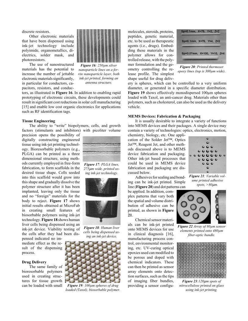
discrete resistors.Other electronic materials
that have been dispensed usingink-jet technology includepolyimide, organometallics, di-electrics, solder mask, andphotoresistors.
The use of nanostructuredmaterials has the potential toincrease the number of jettableelectronic materials significantly,in particular for conductors, ca-pacitors, resistors, and conduc-tors, as illustrated in Figure 16. In addition to enabling rapidprototyping of electronic circuits, these developments couldresult in significant cost reductions in solar cell manufacturing[15] and enable low cost organic electronics for applicationssuch as RF identification tags.
Tissue EngineeringThe ability to “write” biopolymers, cells, and growth
factors (stimulants and inhibitors) with picoliter volumeprecision opens the possibility ofdigitally constructing engineeredtissue using ink-jet printing technol-ogy. Bioresorbable polymers (e.g.,PLGA) can be printed as a threedimensional structure, using meth-ods currently employed in free-formfabrication, to form scaffolds in thedesired tissue shape. Cells seededinto this scaffold would grow intothis shape and gradually dissolve thepolymer structure after it has beenimplanted, leaving only the tissueand no “foreign” materials for thebody to reject. Figure 17 showsinitial results obtained at MicroFabin creating small features ofbiosorbable polymers using ink-jettechnology. Figure 18 shows humanliver cells being dispensed using anink-jet device. Viability testing ofthe cells after they had been dis-pensed indicated no im-mediate effect as the re-sult of the dispensingprocess.
Drug DeliveryThe same family of
bioresorbable polymersused in creating struc-tures for tissue growthcan be loaded with small
molecules, steroids, proteins,peptides, genetic material,etc. to be used as therapeuticagents (i.e., drugs). Embed-ding these materials in thepolymer allows for con-trolled release, with the poly-mer formulation and the ge-ometry controlling the re-lease profile. The simplestshape useful for drug deliv-ery is spheres, which can be controlled to a very uniformdiameter, or generated in a specific diameter distribution.Figure 19 shows effectively monodispersed 100µm spheresloaded with Taxol, an anti-cancer drug. Materials other thanpolymers, such as cholesterol, can also be used as the deliveryvehicle.
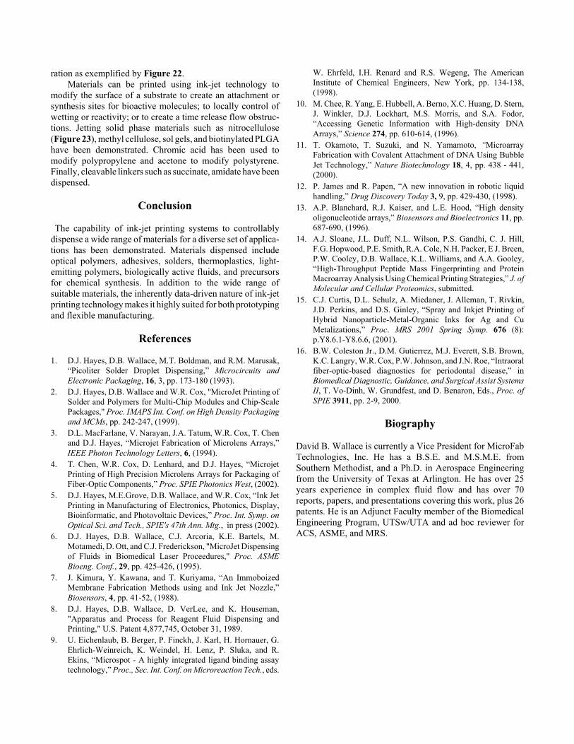
MEMS Devices: Fabrication & PackagingIt is usually desirable to integrate a variety of functions
into MEMS devices and their packages. A single device maycontain a variety of technologies: optics, electronics, motion,chemistry, biology, etc. One appli-cation of the Solder Jet™, OpticsJet™, Reagent Jet, and other meth-ods discussed above is to MEMSdevice fabrication and packaging.Other ink-jet based processes thatcould be used in MEMS devicefabrication and packaging are dis-cussed below.
Adhesives for sealing and bond-ing can be ink-jet printed. Simpleline (Figure 20) and dot patterns canbe applied. In addition, com-plex patterns that vary boththe spatial and volume distri-bution of adhesive can beprinted, as shown in Figure21.
Chemical sensor materi-als can be ink-jet printedonto MEMS devices for usein clinical diagnosis [16],manufacturing process con-trol, environmental monitor-ing, etc. UV-curing opticalepoxies used can modified tobe porous and doped withchemical indicators. Thesecan then be printed as sensorarray elements onto detec-tion surfaces, such as the tipsof imaging fiber bundles,providing a sensor configu-
2. D.J. Hayes, D.B. Wallace and W.R. Cox, "MicroJet Printing ofSolder and Polymers for Multi-Chip Modules and Chip-ScalePackages," Proc. IMAPS Int. Conf. on High Density Packagingand MCMs, pp. 242-247, (1999).
3. D.L. MacFarlane, V. Narayan, J.A. Tatum, W.R. Cox, T. Chenand D.J. Hayes, “Microjet Fabrication of Microlens Arrays,”IEEE Photon Technology Letters, 6, (1994).
4. T. Chen, W.R. Cox, D. Lenhard, and D.J. Hayes, “MicrojetPrinting of High Precision Microlens Arrays for Packaging ofFiber-Optic Components,” Proc. SPIE Photonics West, (2002).
5. D.J. Hayes, M.E.Grove, D.B. Wallace, and W.R. Cox, “Ink JetPrinting in Manufacturing of Electronics, Photonics, Display,Bioinformatic, and Photovoltaic Devices,” Proc. Int. Symp. onOptical Sci. and Tech., SPIE's 47th Ann. Mtg., in press (2002).
6. D.J. Hayes, D.B. Wallace, C.J. Arcoria, K.E. Bartels, M.Motamedi, D. Ott, and C.J. Frederickson, "MicroJet Dispensingof Fluids in Biomedical Laser Proceedures," Proc. ASMEBioeng. Conf., 29, pp. 425-426, (1995).
7. J. Kimura, Y. Kawana, and T. Kuriyama, “An ImmoboizedMembrane Fabrication Methods using and Ink Jet Nozzle,”Biosensors, 4, pp. 41-52, (1988).
8. D.J. Hayes, D.B. Wallace, D. VerLee, and K. Houseman,"Apparatus and Process for Reagent Fluid Dispensing andPrinting," U.S. Patent 4,877,745, October 31, 1989.
9. U. Eichenlaub, B. Berger, P. Finckh, J. Karl, H. Hornauer, G.Ehrlich-Weinreich, K. Weindel, H. Lenz, P. Sluka, and R.Ekins, “Microspot - A highly integrated ligand binding assaytechnology,” Proc., Sec. Int. Conf. on Microreaction Tech., eds.
W. Ehrfeld, I.H. Renard and R.S. Wegeng, The AmericanInstitute of Chemical Engineers, New York, pp. 134-138,(1998).
10. M. Chee, R. Yang, E. Hubbell, A. Berno, X.C. Huang, D. Stern,J. Winkler, D.J. Lockhart, M.S. Morris, and S.A. Fodor,“Accessing Genetic Information with High-density DNAArrays,” Science 274, pp. 610-614, (1996).
11. T. Okamoto, T. Suzuki, and N. Yamamoto, “MicroarrayFabrication with Covalent Attachment of DNA Using BubbleJet Technology,” Nature Biotechnology 18, 4, pp. 438 - 441,(2000).
12. P. James and R. Papen, “A new innovation in robotic liquidhandling,” Drug Discovery Today 3, 9, pp. 429-430, (1998).
13. A.P. Blanchard, R.J. Kaiser, and L.E. Hood, “High densityoligonucleotide arrays,” Biosensors and Bioelectronics 11, pp.687-690, (1996).
14. A.J. Sloane, J.L. Duff, N.L. Wilson, P.S. Gandhi, C. J. Hill,F.G. Hopwood, P.E. Smith, R.A. Cole, N.H. Packer, E J. Breen,P.W. Cooley, D.B. Wallace, K.L. Williams, and A.A. Gooley,“High-Throughput Peptide Mass Fingerprinting and ProteinMacroarray Analysis Using Chemical Printing Strategies,” J. ofMolecular and Cellular Proteomics, submitted.
15. C.J. Curtis, D.L. Schulz, A. Miedaner, J. Alleman, T. Rivkin,J.D. Perkins, and D.S. Ginley, “Spray and Inkjet Printing ofHybrid Nanoparticle-Metal-Organic Inks for Ag and CuMetalizations,” Proc. MRS 2001 Spring Symp. 676 (8):p.Y8.6.1-Y8.6.6, (2001).
16. B.W. Coleston Jr., D.M. Gutierrez, M.J. Everett, S.B. Brown,K.C. Langry, W.R. Cox, P.W. Johnson, and J.N. Roe, “Intraoralfiber-optic-based diagnostics for periodontal disease,” inBiomedical Diagnostic, Guidance, and Surgical Assist SystemsII, T. Vo-Dinh, W. Grundfest, and D. Benaron, Eds., Proc. ofSPIE 3911, pp. 2-9, 2000.
ration as exemplified by Figure 22.Materials can be printed using ink-jet technology to
modify the surface of a substrate to create an attachment orsynthesis sites for bioactive molecules; to locally control ofwetting or reactivity; or to create a time release flow obstruc-tions. Jetting solid phase materials such as nitrocellulose(Figure 23), methyl cellulose, sol gels, and biotinylated PLGAhave been demonstrated. Chromic acid has been used tomodify polypropylene and acetone to modify polystyrene.Finally, cleavable linkers such as succinate, amidate have beendispensed.
Conclusion
The capability of ink-jet printing systems to controllablydispense a wide range of materials for a diverse set of applica-tions has been demonstrated. Materials dispensed includeoptical polymers, adhesives, solders, thermoplastics, light-emitting polymers, biologically active fluids, and precursorsfor chemical synthesis. In addition to the wide range ofsuitable materials, the inherently data-driven nature of ink-jetprinting technology makes it highly suited for both prototypingand flexible manufacturing.
References
Biography
David B. Wallace is currently a Vice President for MicroFabTechnologies, Inc. He has a B.S.E. and M.S.M.E. fromSouthern Methodist, and a Ph.D. in Aerospace Engineeringfrom the University of Texas at Arlington. He has over 25years experience in complex fluid flow and has over 70reports, papers, and presentations covering this work, plus 26patents. He is an Adjunct Faculty member of the BiomedicalEngineering Program, UTSw/UTA and ad hoc reviewer forACS, ASME, and MRS.