Date post: | 30-May-2018 |
Category: |
Documents |
Upload: | mohamed-mahmoud-saad-hassan |
View: | 215 times |
Download: | 0 times |
8/9/2019 Solid State Devices Notes pages 1-27
http://slidepdf.com/reader/full/solid-state-devices-notes-pages-1-27 1/27
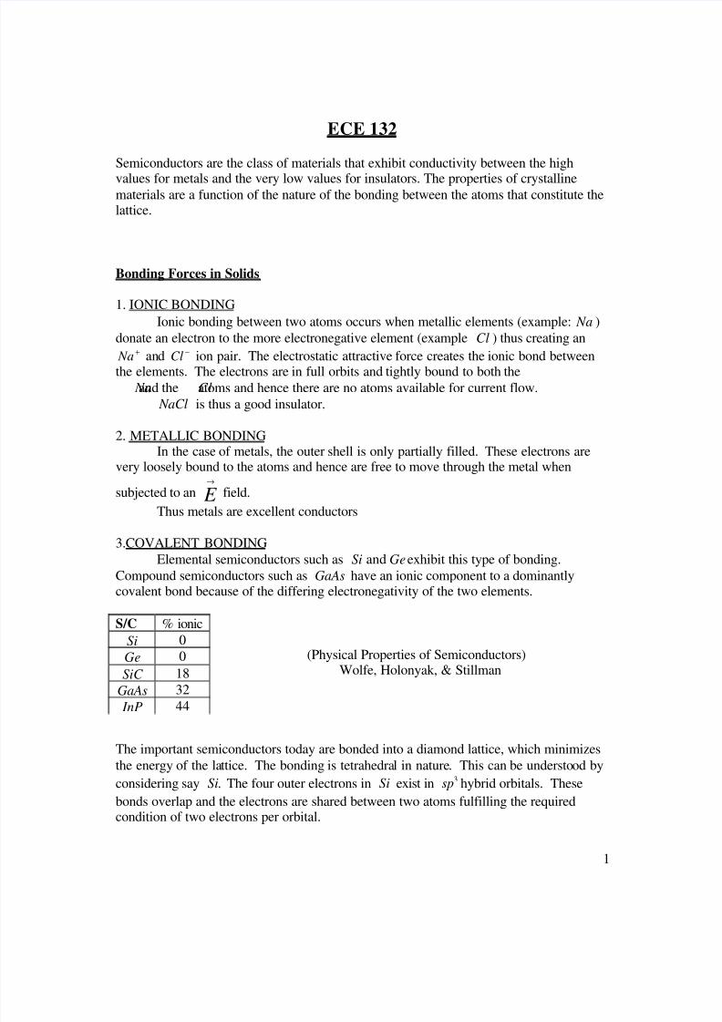
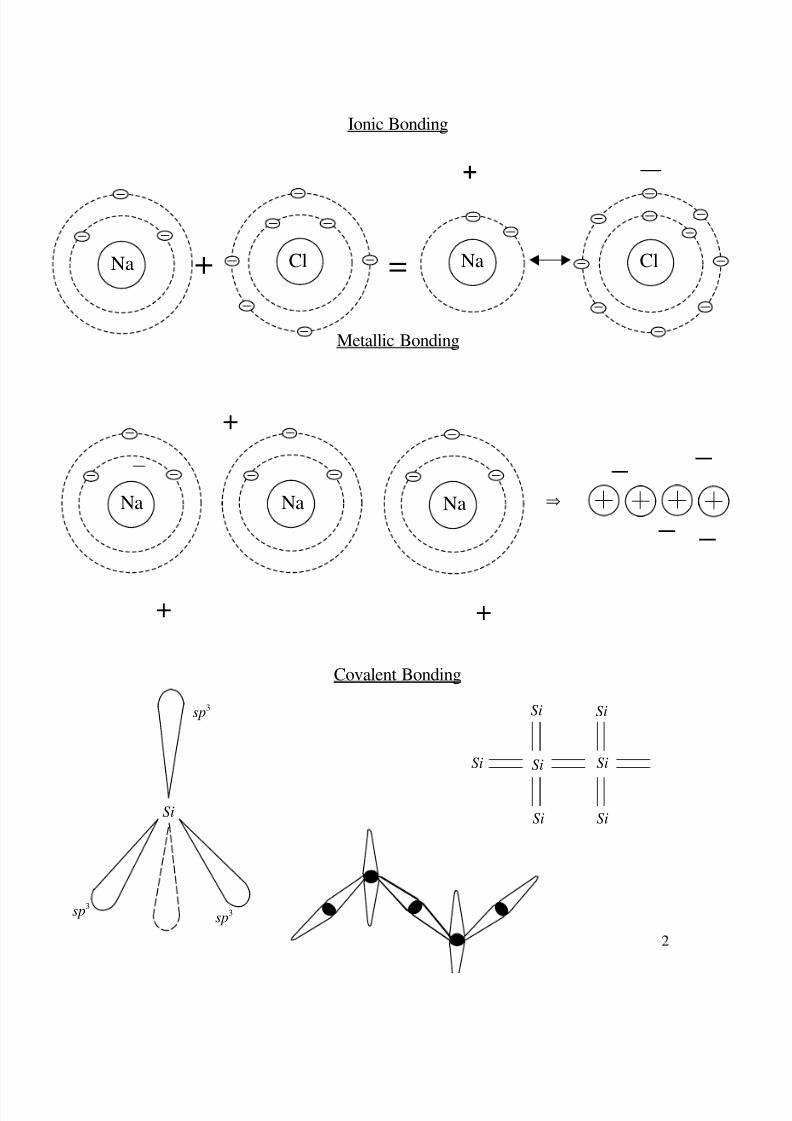
1
ECE 132
Semiconductors are the class of materials that exhibit conductivity between the high
values for metals and the very low values for insulators. The properties of crystallinematerials are a function of the nature of the bonding between the atoms that constitute thelattice.
Bonding Forces in Solids
1. IONIC BONDING
Ionic bonding between two atoms occurs when metallic elements (example: Na )
donate an electron to the more electronegative element (example Cl ) thus creating an
Na + and Cl − ion pair. The electrostatic attractive force creates the ionic bond betweenthe elements. The electrons are in full orbits and tightly bound to both the
and the Na Clatoms and hence there are no atoms available for current flow.
NaCl is thus a good insulator.
2. METALLIC BONDINGIn the case of metals, the outer shell is only partially filled. These electrons are
very loosely bound to the atoms and hence are free to move through the metal when
subjected to an E →
field.
Thus metals are excellent conductors
3.COVALENT BONDING
Elemental semiconductors such as andSi Ge exhibit this type of bonding.
Compound semiconductors such as GaAs have an ionic component to a dominantlycovalent bond because of the differing electronegativity of the two elements.
(Physical Properties of Semiconductors)Wolfe, Holonyak, & Stillman
The important semiconductors today are bonded into a diamond lattice, which minimizes
the energy of the lattice. The bonding is tetrahedral in nature. This can be understood by
considering say .Si The four outer electrons in Si exist in 3sp hybrid orbitals. These
bonds overlap and the electrons are shared between two atoms fulfilling the requiredcondition of two electrons per orbital.
S/C % ionic
Si 0
Ge 0
SiC 18
GaAs 32
InP 44
8/9/2019 Solid State Devices Notes pages 1-27
http://slidepdf.com/reader/full/solid-state-devices-notes-pages-1-27 2/27
2
Ionic Bonding
Metallic Bonding
Covalent Bonding
+
+
++
⇒ Na Na Na
_
_ _
_
Si
Si Si
Si Si Si
SiSi
3sp
3sp3sp
=
+
ClNa Cl Na
8/9/2019 Solid State Devices Notes pages 1-27
http://slidepdf.com/reader/full/solid-state-devices-notes-pages-1-27 3/27
3
Another Pictorial Representation
The energy levels of a hydrogen atom is obtained as
4 2
2 2 2
13.6
2
r n
m e z eV E
n n= − = −
h
This is obtained by solving the Schrödingerequation for a coulombic potential.
Solid Next band is empt
(conduction band)
Last-filled band
(valence band)
Full of
electrons
+Z z is the atomic number
Single atom
2
( ) Ze
V r r
−=
Energy levels, n E
8/9/2019 Solid State Devices Notes pages 1-27
http://slidepdf.com/reader/full/solid-state-devices-notes-pages-1-27 4/27
4
Note that the energy gaps between the quantized energy levels in a single atom are theorigin of the band gap for solids. Typical numbers for band gap for various solids:
This is the MINIMUM energyrequired to allow an electron to leave the (mostly) full valence band and occupy a state in
the conduction band. An analogy is say a football stadium.
The step height is analogous to the band gap in that an energy difference less than thestep height will not get you to the next step. The energy required to move an electron
from the valence band (VB) to the conduction band (CB) is related to the bond strengthand can be provided by one of several means; thermal, light (photons), high energyparticles, etc. Thermal energy exists in each solid at temperatures T>OK. A measure of
thermal energy is Bk T where Bk is the Boltzmann’s constant and 25 9 Bk T meV ⋅: at
room temperature (300K by convention). 1 eV = Energy required to move one electron
up a potential energy of 191 1 6 x 10V −= ⋅ coulombs 191 1 6 x 10V
−= ⋅ Joules.
Semiconductor
1 1
1 4
0 7
g E
Si eV
GaAs eV
Ge eV
⋅⋅⋅
2 9 0
3 4
SiO eV
GaN eV
⋅
⋅
c E
v E
1 1 eV ⋅
iS
c E
v E
GaAs
1 4 eV ⋅
c E
v E
GaN
3 4 eV ⋅
c E
v E
9 0 eV ⋅
2SiO
Field
Step height : Band gap
SEATS
8/9/2019 Solid State Devices Notes pages 1-27
http://slidepdf.com/reader/full/solid-state-devices-notes-pages-1-27 5/27
5
At room temperature pure Si has an intrinsic carrier concentration of 10 31 5 x 10 cm or−⋅ 121 electron/10 atoms.Si
To increase the conductivity of the semiconductors add impurities to make the s/c
extrinsic.
Extrinsic Semiconductors
Creation of free electrons or holes by the addition of impurities is called doping.
N-Type Case (Electrons are majority carriers)
If a group V atom is introduced into the crystal so that it replaces a Si atom.
(i.e. SUBSTITUTIONAL IMPURITY) then the Si lattice looks like such
Si Si Si
Si Si Si P Si
Si Si Si
The P atom incorporates into the lattice through tetrahedral covalent bonding but has an
excess electron that is unpaired and weakly bonded. P in a Si lattice now lookshydrogenic.The electron at finite temperatures is stripped from the P atom or DONATED to the
crystal and is free. Hence the name DONOR atom to group V elements like P in
semiconductors like .Si When the electron is no longer bound to the P atom the P atomhas a net positive charge.
The binding energy of the electron can be calculated as
( )
4 2
22( )2 4
nd c d
q z m E E E
n hπ
∗
∆ = − = ∈
the energy required to make the electron freei.e. to place it in the conduction band.
2
2
13.6 e
d
r
z m E eV
n m
∗ ∆ = ∈
g
Si
8/9/2019 Solid State Devices Notes pages 1-27
http://slidepdf.com/reader/full/solid-state-devices-notes-pages-1-27 6/27
8/9/2019 Solid State Devices Notes pages 1-27
http://slidepdf.com/reader/full/solid-state-devices-notes-pages-1-27 7/27
7
As i Eg n↑ ↓
(1.1 )eV Si 10 31.45 x 10 cm−
Eg (1.4 ) GeV aAs 6 31.79 x 10 cm−
Study the nature of ( ) f E
At 0T K =
( )( 0) f E T = =
1 for
0 for
F
F
E E
E E
<>
It is impossible for electrons to occupy energy above F E at 0T K =
At finite T
( ) f E is the probability of occupancy of an AVAILABLE STATE. ∴ if no state exists
and even is ( ) 1 f E = there will be no electron at that energy.
In a semiconductor
5
23
8 62 x 10
138 x 10
eV k
B
J k
k −
−
=
=
g
g
@ 300 26 Bk T T K meV = =
1
11
2
1
1 2
d d
d F
a
a F
N N E E
ekT
Na N E E e
kT
+
−
=− +
=−+
0T =
1 0T >
2 1T T >
F E
8/9/2019 Solid State Devices Notes pages 1-27
http://slidepdf.com/reader/full/solid-state-devices-notes-pages-1-27 8/27
8
At finite T there is a creation of a hole population (or a lack of an electron population) in
the valence band. ∴ ( ) 1 f E < NOTE:
§ ( ) f E has a finite value in the forbidden gap but no electron exists because there
are no states.
§ ( ) f E is symmetrical about F E .
§ ( ) is the probability of occupancy of a state by an electron f E
1 ( ) f E − is the probability of lack of occupancy of a state or the
probability of occupancy by a hole.
Rewriting
( ) /
1( ) ( )
1 F n E E kT
f E f E e
−= =+
( )/
( ) / ( )/
1( ) 1 ( ) 1
1 1
F
F F
E E kT
p E E kT E E kT
e f E f E
e e
−
− −= − = − =+ +
or ( )/
1( )
1 F p E E kT
f E e
−=+
NOTE THE SYMMETRY OF ELECTRON AND HOLE PROBABILTY ABOUT .F E
v E
i F E E = for an intrins
semiconduct
c E
12
0
v E
c E
( ) f E 1
8/9/2019 Solid State Devices Notes pages 1-27
http://slidepdf.com/reader/full/solid-state-devices-notes-pages-1-27 9/27
9
In Intrinsic Si
o on p= Since the concentration is equal, the Fermi level should lie close to the center of
the gap
is closer to in n-type material and closer toF c E E ∴
Equilibrium Electron and Hole Densities
To calculate the number of electrons in the CB we must know1) How many states are available2) What is the probability of occupancy
We thus introduce
( ) N E dE @ DENSITY OF STATES ( 3cm
− ) available for occupancy in the energy
range dE
∴ Total number of electrons in the CB can be written as
3
Top of
( ) ( ) (electrons )
Bottom of
CB
n f E N E dE cm
CB
−= ∫ g
c E
(for this class the
derivation is not required)
12
0
c E
F E
v E
0
1
1
c E
F E
v E
F E
v E
0
12
1
Intrinsic typen − type p −
8/9/2019 Solid State Devices Notes pages 1-27
http://slidepdf.com/reader/full/solid-state-devices-notes-pages-1-27 10/27
10
At room temperature 0.026kT eV =
We saw that if 4C F E E kT − = then the probability of occupancy of states atmin
C E ( ) / 4( ) 0.0183C F E E kT
C f E e e− − −= = =
For higher energies the ( ) f E drops sharply
Example:( ) / 10 6
0.000045 45 x 10F E E kT
e e− − − −
= = =
∴ the contribution to the integral at higher E is reduced to the point that
Top of
( ) ( ) ( ) = ( ) ( ) ( )
of of
CB
n N E f E d E N E f E d E
B cB B cB
∞= ∫ ∫
Using quantum mechanics and includingPauli’s Principle
( )
32
12
2 2
1 2( )
2
e
c
m N E E E
π
∗ = −
h
2
h
π=h
34
15
6 63 x 10
4.14 x 10 eV-s
h J s−
−
= ⋅ −
=
( ) N E ( ) f E
c E E −
max
c E
min
c E
We know that
( ) /
1( )
1 F E E RT
f E e
−=
+(Fermi-Diriac Statistics)
If 4F E E kT − >
( )
( ) / 1
1
F
F
E E kT
E E e
e
− −− =
+
Since
5
4 6
148
55 406
etc.
F
e E E
e e ekT
= − = = =
8/9/2019 Solid State Devices Notes pages 1-27
http://slidepdf.com/reader/full/solid-state-devices-notes-pages-1-27 11/27
11
Here em∗ is the density of state effective mass
( )( )
32
1 / 22 2
1 2
2
F
c
e E E kT
c
E
mn E E e dE
π
∞ ∗− −
= −
∫ g g g
h
Multiplying and dividing by
( )3
2 we getkT =
( ) ( )3 1
2 2 /
2 2
1 2
2
F E E kT e c E E m dE
n ekT kT π
∗− − −
=
∫ g g g gh
Define c E E u
kT
−@
( )3 12 2
2 2
/ 1 2
2
c
cF e c c
E E E E kT kT E E E E m kT
n e e d kT kT π
∗
−−− − − ∴ = ∫
g g gh
( )
32
12
2 2
0
/ 1 2
2
cF e u du E E kT m kT n e e u
π
∗−−
∞ ∴ =
∫ g g
h
12
0
(From definite integral tables)2
ue u du
π∞
− =∫ g
( )
3
2
2
/ 22 cF e E E kT m kT
n eπ ∗ − =
g g
hor
( ) / c F E E kT
cn N e− −=
32
2
22 Effective density of states in thee
c
m kT N CB
h
π∗
=
@
i.e. Instead of considering the occupancy by electrons of all the states frommin
c E tomax
,c c E N gives us the number of electrons in the CB by considering all the states
in the band to be effectively at the band edge populated with a probability
function( ) /
.c F E E kT e
− −
Likewise, proceeding in a similar manner for the holes in the VB we obtain
8/9/2019 Solid State Devices Notes pages 1-27
http://slidepdf.com/reader/full/solid-state-devices-notes-pages-1-27 12/27
12
( )
32
2
/
2where 2 p
F V
v
kT
v
E E RT p N e
m N
h
π ∗
− −=
=
Effective density of states in thev N VB=
It is clear now that in n type material F E is close to c E and as ( ) c F E E n− ↓ ↑ .
Similarly as ( )F v E E − P↓ ↑ ORc
E
F E
v E
As and
and and
F
F
E n p
E n p
↑ ↑ ↓↓ ↓ ↑
Examine the product n pg
( ) ( )
( )
( )
( )
/ /
/
/
/
or
c F F v
c F F v
c v
c v
g
E E kT E E k T
c v
E E E E kT
c v
E E kT
c v
E E kT
c v
c v g
E
kT c v
n p N N e e
N N e
np N N e
np N N e
E E E
np N N e
− − − −⋅ ⋅
− + − +⋅
− −
− −
−
=
=
=
=
− =
=
g
The expressions for and are applicable for all types of semiconductors: , orn p n p i
In an intrinsic material the Fermi Level is identified as Fi E
( ) / (intrinsic) Fi c E E kT
i cn n N e−= =
( ) / and (intrinsic) Fi v E E kT
i v p p N e− −= =
( )2 - - / c v E E kT
i i i c vn p n N N e∴ = =
/ g E kT
i c vn N N e
−=
Note that( )2 /
c v E E kT
i c vnp n N N e− −=
Moves towards c E for typen −
Moves towards v E for type p −
8/9/2019 Solid State Devices Notes pages 1-27
http://slidepdf.com/reader/full/solid-state-devices-notes-pages-1-27 13/27
13
Now that we can relate F E to thenature of the andCB VB through
andn pm m∗ ∗
we can recalculate, ,iF E
more accurately. Anyasymmetry in &n p distribution
has to be introduced through
differences in &c v N N .
( ) / 2 c Fi
Eg E E kT kT
i c c vn N e N N e−− −= =
( ) / 2 c Fi
Eg E E kT v kT
c
N e e
N
−− −⇒ =
exp exp2
exp / 2
c Fi v
c
vc Fi
c
E E N Eg
kT kT N
N Eg E E kT
N
− +∴ • =
⇒ − + + =
Taking ln of both sides
ln2
v
c Fi
c
N Eg E E kT
N − + + =
Since g c v E E E = −
ln2 2
c v v
Fi c
c
E E N E E kT
N = − − +
∴ v
c
N1ln
2 2 N
c vFi
E E E kT
+= +
The second turn is the derivation
of iF E from the middle of the gap.
1
2
0
c E
F E
v E
8/9/2019 Solid State Devices Notes pages 1-27
http://slidepdf.com/reader/full/solid-state-devices-notes-pages-1-27 14/27
14
So what is the dependence of vs ?n T
Space Charge Neutrality
We can dope a semiconductor with both donors and acceptors
Donate electrons ↵ ] Accept electronsi.e. remove electrons
effective
effective
for n-type material
for p-type
d A
a d
n N N
p N N
≅ −≅ −
These materials are called compensated semiconductors.
( )
( )
/
/
and
c F
F v
E E kT
c
E E kT
v
n N e
p N e
− −
− −
=
=
In a bulk semiconductor there must be charge neutrality everywhere because any excesscharge will immediately set up an electric field.
Low temp
1710
1510
1310
Hightemp
1000/ T
n Nd Nd +≅ <
Intrinsic
Freeze-outExtrinsic
region
are still valid relations.
8/9/2019 Solid State Devices Notes pages 1-27
http://slidepdf.com/reader/full/solid-state-devices-notes-pages-1-27 15/27
15
Q E F q
eE →
= = −
The electrons will flow towards the positive charge until the value is reduced to 0.Q
Then 0. The attractive force, 0. E F → ⇒ →
o D o p N n N
A
−++ = + Bulk semiconductor at equilibrium
o D A on N N p−
+ = − +
i E
Conductivity and Mobility
+
+
+
+ +
+++
Q E
F qE = −
o D An N N + −−; or neglecting o
p
Ed
Ea
F E
8/9/2019 Solid State Devices Notes pages 1-27
http://slidepdf.com/reader/full/solid-state-devices-notes-pages-1-27 16/27
16
At any temperature the individual electrons show randomized motion. Scattering with
the lattice is the dominant randomizing process. If we apply a field, x E then
/per electron xF qE = −
∴ Net change of momentum of the electron ensemble=
3where # of electrons/cm
x
dpnqE
dt
n
= −
=
We want to use this equation to determine the response of an electron to an appliedelectric field.
i.e. The relationship between its velocity and the applied field.
Assume:
1) The probability of collision is constant2) # of electons in the group at 0o
N t = =
3) ( ) # of electrons which have not undergone collisions by time N t t =
Let the scattering rate or number of collisions/sec be K .
∴ The rate of decrease of ( ) , N t the scattered population is given by
( )( ) (assumption #1)
( )
ln ( )( )
dN t KN t
dt
dN t Kdt N t Kt c
N t
= −
∴ = − ⇒ = − +
Since ( )0 , lno o N t N c N = = =
∴ ( ) Kt
o N t N e
−=
t −
8/9/2019 Solid State Devices Notes pages 1-27
http://slidepdf.com/reader/full/solid-state-devices-notes-pages-1-27 17/27
17
Let t −
be the mean time between collisions
( )
( )
Kt
o
Kt
o
N te dt t N t dt t
N t dt N e dt
−−
−
∞∞
∞ ∞=∫ ∫
∫ ∫ oo
o o
@ so 1 t K
−= and ( )
t t
o N t N e−
=
The probability that an electron will experience a collision in an interval dt is .dt
t − This
is equivalently the fraction of electrons that undergo a collision. Let x p be the
momentum in the direction. x −
because momemtum decreases
x x
dt dp p
t −∴ = −
↑
or rate of decrease of due to collisions x x x
dp p p
dt t −
−=
rate of increase of due to x x x x
dpqnE p E
dt = −
At steady state rate of momentum increase due to x E = rate of momentum decrease due to
collision.
, the average momentum/electron
x x x x
x x x
PqnE P n q t E
t
PP q t E
n
−
−
−
∴ = − ⇒ = −
∴< > = −@
x x x
n n
P q t E V
m m
−
∗ ∗
< > −∴ < >= =
Introduce the concept of mobility
2 1 1 n
x n n xn
q t V E cm V s
mµ µ
−
− −∗< > = − ⇒ =
p
x p x p p
q t V E
mµ µ
−
∗= ⇒ =
8/9/2019 Solid State Devices Notes pages 1-27
http://slidepdf.com/reader/full/solid-state-devices-notes-pages-1-27 18/27
18
x nV < > is the net drift of the electron distribution under the influence of x
E .
The current density resulting from the drift velocity is
nx x n
px x p
J qn V
J qp V
= − < >
= + < >
2
.nx x
n n
q t q n t J qn E E
m m
− −
∗ ∗
− + ∴ = − =
Rewriting as conventional Ohm’s Law
2
Note :
nx n x n
n
n n p p
nq t J E
m
qn qp
σ σ
σ µ σ µ
−
∗=
= =
@
If both electrons and holes are present
( ) x p x nx n p x J J J q n p E µ µ= + = +
Since the probabilities of scattering add 1 2K K K = +
1 1Since i
i
K
it α
µ−=
1 2
1 1 1
µ µ µ= + Matthiesen’s Rule
Measurement of Semiconductor Parameters
1) Effective mass m∗ can be determined by electron resonance. Under a magnetic field
the electron motion is circular.
energy RF
Lattice
scattering
32
T
−32
T
Impurity
scattering
2
Centripetal force magnetic flux density
mvqvB
r =
↑Zv B
8/9/2019 Solid State Devices Notes pages 1-27
http://slidepdf.com/reader/full/solid-state-devices-notes-pages-1-27 19/27
19
or c
qBr qBv
m mω∗ ∗∴ = = =
If RF energy is incident on the sample it will be transmitted for all frequencies except
cω when resonance absorption of energy occurs. (Reduced transmission)
By measuring cω we can calculate orn pm m∗ ∗ .
2) Mobility (Hall Effect) and Carrier Concentration
z
y
x
Consider a p-type bar, which is subject to an electric field x E and a magnetic field z B .
The force on a single hole
( )
y y x z
F q E V x B
F q E v B
→ → → = +
∴ = −
y E is the electric field that is set up by the holes that were deflected under the influence
of the force . x zv B Since no current can flow in the y-direction.
0 y y x zF E v B= ⇒ =
The xv can be obtained from x J as
where hole concentration x x o
o
J v p
qp= =
+
Cyclotron resonance
frequency
y E
x E
L
w
x I
z B
t
AV
DV
BV
cV
8/9/2019 Solid State Devices Notes pages 1-27
http://slidepdf.com/reader/full/solid-state-devices-notes-pages-1-27 20/27
20
x y z H x z
o
J E B R J B
qp∴ = =g
Where1
Hall Coefficient H
o
Rqp
= =
1 x z x
x o
H y
x z A B AB y o
AB
J B I J p
wt qR qE
I BV V V E p
w w qtV
= ∴ = =
−= = =
1 /
where /
CD x
o o
V I Rwt
qp qp L L wt
σµ = = = =
Excess Carriers in Semiconductors :
The beam is absorbed
( )( )
( ) x
o
dI x I x
dx
I x I e α
α
−
− =
⇒ =
absorption coefficient
is the energy of the photon in .
1 24( )
( )
eV
hc eV hv E
mλ λ µ
⋅= = =
14444244443
hv Eg>
emission of light
(direct semiconductor)
generation
Recombination
Eg
1( )cmα −
E
8/9/2019 Solid State Devices Notes pages 1-27
http://slidepdf.com/reader/full/solid-state-devices-notes-pages-1-27 21/27
21
Carrier Lifetime & Photoconductivity
Let us calculate the rate of change in the electron population when I switch the light off.
We first assume that the rate of recombination, R , is proportional to the product of the
electron and hole population. For example: ( ) ( ) .r R p t n t α= g g In the absence of light thethermal generation rate should be equal to the thermal recombination rate.
or2
th th r i i r iG R n p nα α⋅ ⋅= = =
Now( )
th
dn t G R G R
dt = − = −
2( )( ) ( )r i r
dn t n n t p t
dt α α= −
Recognizing that on shining light equal numbers of e and hole pairs are created
( ) ( )( )n t p t δ δ= , and since2
r i r o on n pα α ⋅= ,
( ) [ ][ ]2( ) ( )i r o o
d n t n n n t p p t
dt
δ α α δ δ= − + +
[ ]2( ) ( ) ( )r o on p n t n t α δ δ= − + +
Low level injection
P-type material
∴ ( ) ( )
2ando o on p n t n t pδ δ⇒ <
g=
( )
( )1
r
( )
( )
Recombination time
Also the minority carrier lifetime
r o
o n
t r o n
t p
d n t p n t
dt
n t n e n e
p
α τ
δ α δ
δ
α τ−
−−
⇒ = −
⇒ = ∆ = ∆
= =
THIS ANALYSIS IS VALID ONLY FOR DIRECT RECOMBINATION
Thermal generation rate
(In the absence of light)
8/9/2019 Solid State Devices Notes pages 1-27
http://slidepdf.com/reader/full/solid-state-devices-notes-pages-1-27 22/27
22
Not valid for recombination via traps
Quasi-Fermi level [ ]IMREF
( ) r o og t n pα= ; in steady state since generation rate = recombination rate
We know with light ( )( )( ) oP r r o og T g np n n p pα α δ δ+ = = + +
In steady state with no trapping n pδ δ=
( ) ( )2( )
oP r o o r o og T g n p n p n nα α δ δ + = + + +
[ ]
In general
If
op r o
n
op n n op
p op
n
g p n
n
n g n g
p g
α δ
δ
τ
δ τ δ τ
δ ττ τ
=
=
⇒ = =
=≠ p
( )
( )
Fn i
i Fp
E E
o i
E E RT
o i
n n n n e
p p p n e
δ
δ
−
−
+ = =
+ = =
Electron IMREF
Hole IMREF
Fn
Fp
E
E
==
Diffusion of Carriers
Eg
Ev
In general traps reduce the
minority carrier lifetime evenfurther
( )n x
(diffusion)nφ
[Low level injection in a p − type material
and ]o o on p n pδ⇒ < <
8/9/2019 Solid State Devices Notes pages 1-27
http://slidepdf.com/reader/full/solid-state-devices-notes-pages-1-27 23/27
23
( )( )
The negative sign represents diffusion from higher to lower concentration
n n
dn x x D
dxφ = −
↑
( )( ) p p
dp x x D
dxφ = −
The diffusion current ( )
n n
n n
p p
dn J q D
dx
dn J qD
dx
dp
J qDdx
= − −
=
= −
g
In the presence of an electric field
( ) drift diffusionn n n J x J J = +
( )( )
( ) ( )
( )( ) ( ) ( )
n n n
p p p
dn x J x q n x E x qD
dx
dp x J x q p x E x qD
dx
µ
µ
= +
= −
( ) ( ) ( )n p J x J x J x= +
Continuity Equation
A ( ) Jp x x+ ∆ ( ) Jp x
x x x+ ∆
x∆
A= Area in 2cm and x∆ is the length of the box in
centimeters.
or the total current is the sum
of all electron and hole currents
8/9/2019 Solid State Devices Notes pages 1-27
http://slidepdf.com/reader/full/solid-state-devices-notes-pages-1-27 24/27
8/9/2019 Solid State Devices Notes pages 1-27
http://slidepdf.com/reader/full/solid-state-devices-notes-pages-1-27 25/27
25
2
2
2
2
n
n
p p
n d n n D
t x
p p p
Dt x
δ δ δ
τ
δ δ δ
τ
∂= −
∂ ∂
∂ ∂
= −∂ ∂
Diffusion Length
/ 1 2( )
x
x Lp Lp p x c e c eδ−
∴ = +
As 1we know 0 or 0 x p cδ→ ∞ → =
( ) 2
x Lp p x c eδ
−∴ =
1the distance where the distribution drops to x initial value p L
e=
AND
average distance a hole travels before recombining. p L =
The hole diffusion current can be calculated at any x as
( )( )( )
p
p p
qD dp x d J x qD p
dx dxδ= − = −
p∆
2
22
Consider steady state or 0
n n n
t
n n n
x D L
δ δ δ
τ
∂=
∂∂
⇒ = ≡∂
and2
2 2
p p
p p p
x D Lp
δ δ δ
τ
∂ = ≡∂
Decay is given by the solution to the
above diffusion equationo
P
8/9/2019 Solid State Devices Notes pages 1-27
http://slidepdf.com/reader/full/solid-state-devices-notes-pages-1-27 26/27
26
( ) p
p
qD p x
Lδ=
Currents in relation to &n pF F E E
( )( ) ( ) ( )n n n
dn x J x q n x E x qD
dxµ= +
( ) ( )Since Fn Fi Fn Fi
i
E E dE dE dn x d n xn e
dx dx RT RT dx dx
− = = −
AND since , we getn Dn RT µ=
( ) ( ) ( ) ( ) Fn Fin n n
dE dE J x q n x E x n x
dx dxµ µ = + −
But ( )i
x
dE qE x
dE =
( ) ( ) total electron currentFnn n
dE J x n x
dxµ∴ =
( )( ) dV x E xdx
= −
( ) 1But ( ) ( ) Fi
E E x d dEiV x E x
q dx q q dx
= ⇒ − = − −
c E
v E
No fieldc
E
v E
i E
( ) E x
8/9/2019 Solid State Devices Notes pages 1-27
http://slidepdf.com/reader/full/solid-state-devices-notes-pages-1-27 27/27
What is the relationship between & ? D µ
At equilibrium no current flows in the semiconductor. So, assuming a type p −
semiconductor
( )( ) ( ) 0 p p p
dp x J x q p E x qD
dxµ= − =
1 ( )( )
( )
p
p
D dp x E x
p x dxµ=
( ) / ( ) i F E E RT
i p x n e−=
1( )
p
p
D E x
RT µ⇒ =
D kT
qµ⇒ =
i F dE dE
dx dx
−
qE
0
Einstein’s relation