408

Solid-State Physics for Electronics
André Moliton
Series Editor Pierre-Noël Favennec

This page intentionally left blank

Solid-State Physics for Electronics

This page intentionally left blank

Solid-State Physics for Electronics
André Moliton
Series Editor Pierre-Noël Favennec

First published in France in 2007 by Hermes Science/Lavoisier entitled: Physique des matériaux pour l’électronique © LAVOISIER, 2007 First published in Great Britain and the United States in 2009 by ISTE Ltd and John Wiley & Sons, Inc. Apart from any fair dealing for the purposes of research or private study, or criticism or review, as permitted under the Copyright, Designs and Patents Act 1988, this publication may only be reproduced, stored or transmitted, in any form or by any means, with the prior permission in writing of the publishers, or in the case of reprographic reproduction in accordance with the terms and licenses issued by the CLA. Enquiries concerning reproduction outside these terms should be sent to the publishers at the undermentioned address: ISTE Ltd John Wiley & Sons, Inc. 27-37 St George’s Road 111 River Street London SW19 4EU Hoboken, NJ 07030 UK USA
www.iste.co.uk www.wiley.com © ISTE Ltd, 2009 The rights of André Moliton to be identified as the author of this work have been asserted by him in accordance with the Copyright, Designs and Patents Act 1988.
Library of Congress Cataloging-in-Publication Data Moliton, André. [Physique des matériaux pour l'électronique. English] Solid-state physics for electronics / André Moliton. p. cm. Includes bibliographical references and index. ISBN 978-1-84821-062-2 1. Solid state physics. 2. Electronics--Materials. I. Title. QC176.M5813 2009 530.4'1--dc22
2009016464 British Library Cataloguing-in-Publication Data A CIP record for this book is available from the British Library ISBN: 978-1-84821-062-2
Cover image created by Atelier Istatis. Printed and bound in Great Britain by CPI Antony Rowe, Chippenham and Eastbourne.

Table of Contents
Foreword . . . . . . . . . . . . . . . . . . . . . . . . . . . . . . . . . . . . . . . . . . xiii
Introduction . . . . . . . . . . . . . . . . . . . . . . . . . . . . . . . . . . . . . . . . xv
Chapter 1. Introduction: Representations of Electron-Lattice Bonds . . . . 1 1.1. Introduction . . . . . . . . . . . . . . . . . . . . . . . . . . . . . . . . . . . . 1 1.2. Quantum mechanics: some basics . . . . . . . . . . . . . . . . . . . . . . 2
1.2.1. The wave equation in solids: from Maxwell’s to Schrödinger’s equation via the de Broglie hypothesis. . . . . . . . . . . 2 1.2.2. Form of progressive and stationary wave functions for an electron with known energy (E) . . . . . . . . . . . . . . . . . . . . . 4 1.2.3. Important properties of linear operators . . . . . . . . . . . . . . . . . 4
1.3. Bonds in solids: a free electron as the zero order approximation for a weak bond; and strong bonds . . . . . . . . . . . . . . . . . . . . . . . . . 6
1.3.1. The free electron: approximation to the zero order . . . . . . . . . . 6 1.3.2. Weak bonds . . . . . . . . . . . . . . . . . . . . . . . . . . . . . . . . . 7 1.3.3. Strong bonds . . . . . . . . . . . . . . . . . . . . . . . . . . . . . . . . . 8 1.3.4. Choosing between approximations for weak and strong bonds . . . 9
1.4. Complementary material: basic evidence for the appearance of bands in solids . . . . . . . . . . . . . . . . . . . . . . . . . . . . . . . . . . . . . . . . . 10
1.4.1. Basic solutions for narrow potential wells . . . . . . . . . . . . . . . 10 1.4.2. Solutions for two neighboring narrow potential wells . . . . . . . . 14
Chapter 2. The Free Electron and State Density Functions . . . . . . . . . . 17 2.1. Overview of the free electron . . . . . . . . . . . . . . . . . . . . . . . . . 17
2.1.1. The model . . . . . . . . . . . . . . . . . . . . . . . . . . . . . . . . . . 17 2.1.2. Parameters to be determined: state density functions in k or energy spaces . . . . . . . . . . . . . . . . . . . . . . . . . . . . . . . . . 17

vi Solid-State Physics for Electronics
2.2. Study of the stationary regime of small scale (enabling the establishment of nodes at extremities) symmetric wells (1D model) . . 19
2.2.1. Preliminary remarks . . . . . . . . . . . . . . . . . . . . . . . . . . . . 19 2.2.2. Form of stationary wave functions for thin symmetric wells with width (L) equal to several inter-atomic distances (L a), associated with fixed boundary conditions (FBC) . . . . . . . . . . . . . . 19 2.2.3. Study of energy . . . . . . . . . . . . . . . . . . . . . . . . . . . . . . . 21 2.2.4. State density function (or “density of states”) in k space . . . . . . . 22
2.3. Study of the stationary regime for asymmetric wells (1D model) with L a favoring the establishment of a stationary regime with nodes at extremities . . . . . . . . . . . . . . . . . . . . . . . . . . . . . . 23 2.4. Solutions that favor propagation: wide potential wells where L 1 mm, i.e. several orders greater than inter-atomic distances . . . 24
2.4.1. Wave function . . . . . . . . . . . . . . . . . . . . . . . . . . . . . . . . 24 2.4.2. Study of energy . . . . . . . . . . . . . . . . . . . . . . . . . . . . . . . 26 2.4.3. Study of the state density function in k space . . . . . . . . . . . . . 27
2.5. State density function represented in energy space for free electrons in a 1D system . . . . . . . . . . . . . . . . . . . . . . . . . . . . . . . . . . . . . 27
2.5.1. Stationary solution for FBC . . . . . . . . . . . . . . . . . . . . . . . . 29 2.5.2. Progressive solutions for progressive boundary conditions (PBC) . 30 2.5.3. Conclusion: comparing the number of calculated states for FBC and PBC . . . . . . . . . . . . . . . . . . . . . . . . . . . . . . . . . . 30
2.6. From electrons in a 3D system (potential box) . . . . . . . . . . . . . . . 32 2.6.1. Form of the wave functions . . . . . . . . . . . . . . . . . . . . . . . . 32 2.6.2. Expression for the state density functions in k space . . . . . . . . . 35 2.6.3. Expression for the state density functions in energy space . . . . . . 37
2.7. Problems . . . . . . . . . . . . . . . . . . . . . . . . . . . . . . . . . . . . . 40 2.7.1. Problem 1: the function Z(E) in 1D . . . . . . . . . . . . . . . . . . . 41 2.7.2. Problem 2: diffusion length at the metal-vacuum interface . . . . . 42 2.7.3. Problem 3: 2D media: state density function and the behavior of the Fermi energy as a function of temperature for a metallic state . . . 44 2.7.4. Problem 4: Fermi energy of a 3D conductor . . . . . . . . . . . . . . 47 2.7.5. Problem 5: establishing the state density function via reasoning in moment or k spaces . . . . . . . . . . . . . . . . . . . . . . . . . . . . . . . 49 2.7.6. Problem 6: general equations for the state density functions expressed in reciprocal (k) space or in energy space . . . . . . . . . . . . . 50
Chapter 3. The Origin of Band Structures within the Weak Band Approximation . . . . . . . . . . . . . . . . . . . . . . . . . . . . . . . . . . . . . . 55
3.1. Bloch function . . . . . . . . . . . . . . . . . . . . . . . . . . . . . . . . . . 55 3.1.1. Introduction: effect of a cosinusoidal lattice potential . . . . . . . . 55 3.1.2. Properties of a Hamiltonian of a semi-free electron . . . . . . . . . . 56 3.1.3. The form of proper functions . . . . . . . . . . . . . . . . . . . . . . . 57
Table of Contents vii
3.2. Mathieu’s equation . . . . . . . . . . . . . . . . . . . . . . . . . . . . . . . 59 3.2.1. Form of Mathieu’s equation. . . . . . . . . . . . . . . . . . . . . . . . 59 3.2.2. Wave function in accordance with Mathieu’s equation . . . . . . . 59 3.2.3. Energy calculation . . . . . . . . . . . . . . . . . . . . . . . . . . . . . 63 3.2.4. Direct calculation of energy when
ak . . . . . . . . . . . . . . 64
3.3. The band structure . . . . . . . . . . . . . . . . . . . . . . . . . . . . . . . . 66 3.3.1. Representing E f (k) for a free electron: a reminder . . . . . . . . 66 3.3.2. Effect of a cosinusoidal lattice potential on the form of wave function and energy . . . . . . . . . . . . . . . . . . . . . . . . . . . 67 3.3.3. Generalization: effect of a periodic non-ideally cosinusoidal potential . . . . . . . . . . . . . . . . . . . . . . . . . . . . . . . 69
3.4. Alternative presentation of the origin of band systems via the perturbation method . . . . . . . . . . . . . . . . . . . . . . . . . . . . . 70
3.4.1. Problem treated by the perturbation method . . . . . . . . . . . . . . 70 3.4.2. Physical origin of forbidden bands . . . . . . . . . . . . . . . . . . . . 71 3.4.3. Results given by the perturbation theory . . . . . . . . . . . . . . . . 74 3.4.4. Conclusion . . . . . . . . . . . . . . . . . . . . . . . . . . . . . . . . . . 77
3.5. Complementary material: the main equation . . . . . . . . . . . . . . . . 79 3.5.1. Fourier series development for wave function and potential . . . . 79 3.5.2. Schrödinger equation . . . . . . . . . . . . . . . . . . . . . . . . . . . . 80 3.5.3. Solution . . . . . . . . . . . . . . . . . . . . . . . . . . . . . . . . . . . . 81
3.6. Problems . . . . . . . . . . . . . . . . . . . . . . . . . . . . . . . . . . . . . 81 3.6.1. Problem 1: a brief justification of the Bloch theorem . . . . . . . . . 81 3.6.2. Problem 2: comparison of E(k) curves for free and semi-free electrons in a representation of reduced zones . . . . . . . . 84
Chapter 4. Properties of Semi-Free Electrons, Insulators, Semiconductors, Metals and Superlattices . . . . . . . . . . . . . . . . . . . . . . . . . . . . . . . 87
4.1. Effective mass (m*) . . . . . . . . . . . . . . . . . . . . . . . . . . . . . . . 87 4.1.1. Equation for electron movement in a band: crystal momentum . . 87 4.1.2. Expression for effective mass . . . . . . . . . . . . . . . . . . . . . . . 89 4.1.3. Sign and variation in the effective mass as a function of k . . . . . 90 4.1.4. Magnitude of effective mass close to a discontinuity . . . . . . . . . 93
4.2. The concept of holes . . . . . . . . . . . . . . . . . . . . . . . . . . . . . . 93 4.2.1. Filling bands and electronic conduction. . . . . . . . . . . . . . . . . 93 4.2.2. Definition of a hole . . . . . . . . . . . . . . . . . . . . . . . . . . . . . 94
4.3. Expression for energy states close to the band extremum as a function of the effective mass . . . . . . . . . . . . . . . . . . . . . . . . . 96
4.3.1. Energy at a band limit via the Maclaurin development
(in k = kn =a
n ) . . . . . . . . . . . . . . . . . . . . . . . . . . . . . . . . . . 96
4.4. Distinguishing insulators, semiconductors, metals and semi-metals . . 97

viii Solid-State Physics for Electronics
4.4.1. Required functions . . . . . . . . . . . . . . . . . . . . . . . . . . . . . 97 4.4.2. Dealing with overlapping energy bands . . . . . . . . . . . . . . . . . 97 4.4.3. Permitted band populations . . . . . . . . . . . . . . . . . . . . . . . . 98
4.5. Semi-free electrons in the particular case of super lattices . . . . . . . . 107 4.6. Problems . . . . . . . . . . . . . . . . . . . . . . . . . . . . . . . . . . . . . 116
4.6.1. Problem 1: horizontal tangent at the zone limit (k /a) of the dispersion curve . . . . . . . . . . . . . . . . . . . . . . . . . . . . . . 116 4.6.2. Problem 2: scale of m* in the neighborhood of energy discontinuities . . . . . . . . . . . . . . . . . . . . . . . . . . . . . 117 4.6.3. Problem 3: study of EF(T) . . . . . . . . . . . . . . . . . . . . . . . . . 122
Chapter 5. Crystalline Structure, Reciprocal Lattices and Brillouin Zones 123 5.1. Periodic lattices . . . . . . . . . . . . . . . . . . . . . . . . . . . . . . . . . 123
5.1.1. Definitions: direct lattice . . . . . . . . . . . . . . . . . . . . . . . . . 123 5.1.2. Wigner-Seitz cell . . . . . . . . . . . . . . . . . . . . . . . . . . . . . . 125
5.2. Locating reciprocal planes . . . . . . . . . . . . . . . . . . . . . . . . . . . 125 5.2.1. Reciprocal planes: definitions and properties . . . . . . . . . . . . . 125 5.2.2. Reciprocal planes: location using Miller indices . . . . . . . . . . . 125
5.3. Conditions for maximum diffusion by a crystal (Laue conditions) . . . 128 5.3.1. Problem parameters . . . . . . . . . . . . . . . . . . . . . . . . . . . . 128 5.3.2. Wave diffused by a node located by , ,m n p m a n b p c 129
5.4. Reciprocal lattice . . . . . . . . . . . . . . . . . . . . . . . . . . . . . . . . 133 5.4.1. Definition and properties of a reciprocal lattice . . . . . . . . . . . . 133 5.4.2. Application: Ewald construction of a beam diffracted by a reciprocal lattice . . . . . . . . . . . . . . . . . . . . . . . . . . . . . . . 134
5.5. Brillouin zones . . . . . . . . . . . . . . . . . . . . . . . . . . . . . . . . . 135 5.5.1. Definition . . . . . . . . . . . . . . . . . . . . . . . . . . . . . . . . . . 135 5.5.2. Physical significance of Brillouin zone limits . . . . . . . . . . . . . 135 5.5.3. Successive Brillouin zones . . . . . . . . . . . . . . . . . . . . . . . . 137
5.6. Particular properties . . . . . . . . . . . . . . . . . . . . . . . . . . . . . . . 137 5.6.1. Properties of , ,h k lG and relation to the direct lattice . . . . . . . . 137 5.6.2. A crystallographic definition of reciprocal lattice . . . . . . . . . . . 139 5.6.3. Equivalence between the condition for maximum diffusion and Bragg’s law. . . . . . . . . . . . . . . . . . . . . . . . . . . . . . . . . . . 139
5.7. Example determinations of Brillouin zones and reduced zones . . . . . 141 5.7.1. Example 1: 3D lattice . . . . . . . . . . . . . . . . . . . . . . . . . . . 141 5.7.2. Example 2: 2D lattice . . . . . . . . . . . . . . . . . . . . . . . . . . . 143 5.7.3. Example 3: 1D lattice with lattice repeat unit (a) such that the base vector in the direct lattice is a . . . . . . . . . . . . . . . . . . . . . . . . . . 145
5.8. Importance of the reciprocal lattice and electron filling of Brillouin zones by electrons in insulators, semiconductors and metals . . 146
5.8.1. Benefits of considering electrons in reciprocal lattices . . . . . . . 146

Table of Contents ix
5.8.2. Example of electron filling of Brillouin zones in simple structures: determination of behaviors of insulators, semiconductors and metals . . . 146
5.9. The Fermi surface: construction of surfaces and properties . . . . . . . 149 5.9.1. Definition . . . . . . . . . . . . . . . . . . . . . . . . . . . . . . . . . . 149 5.9.2. Form of the free electron Fermi surface . . . . . . . . . . . . . . . . 149 5.9.3. Evolution of semi-free electron Fermi surfaces . . . . . . . . . . . . 150 5.9.4. Relation between Fermi surfaces and dispersion curves . . . . . . . 152
5.10. Conclusion. Filling Fermi surfaces and the distinctions between insulators, semiconductors and metals . . . . . . . . . . . . . . . . . 154
5.10.1. Distribution of semi-free electrons at absolute zero . . . . . . . . . 154 5.10.2. Consequences for metals, insulators/semiconductors and semi-metals . . . . . . . . . . . . . . . . . . . . . . . . . . . . . . . . . . . 155
5.11. Problems . . . . . . . . . . . . . . . . . . . . . . . . . . . . . . . . . . . . . 156 5.11.1. Problem 1: simple square lattice . . . . . . . . . . . . . . . . . . . . 156 5.11.2. Problem 2: linear chain and a square lattice . . . . . . . . . . . . . 157 5.11.3. Problem 3: rectangular lattice . . . . . . . . . . . . . . . . . . . . . . 162
Chapter 6. Electronic Properties of Copper and Silicon . . . . . . . . . . . . 173 6.1. Introduction . . . . . . . . . . . . . . . . . . . . . . . . . . . . . . . . . . . . 173 6.2. Direct and reciprocal lattices of the fcc structure . . . . . . . . . . . . . . 173
6.2.1. Direct lattice . . . . . . . . . . . . . . . . . . . . . . . . . . . . . . . . . 173 6.2.2. Reciprocal lattice . . . . . . . . . . . . . . . . . . . . . . . . . . . . . . 175
6.3. Brillouin zone for the fcc structure . . . . . . . . . . . . . . . . . . . . . . 178 6.3.1. Geometrical form . . . . . . . . . . . . . . . . . . . . . . . . . . . . . . 178 6.3.2. Calculation of the volume of the Brillouin zone . . . . . . . . . . . . 179 6.3.3. Filling the Brillouin zone for a fcc structure . . . . . . . . . . . . . . 180
6.4. Copper and alloy formation . . . . . . . . . . . . . . . . . . . . . . . . . . 181 6.4.1. Electronic properties of copper . . . . . . . . . . . . . . . . . . . . . . 181 6.4.2. Filling the Brillouin zone and solubility rules . . . . . . . . . . . . . 181 6.4.3. Copper alloys . . . . . . . . . . . . . . . . . . . . . . . . . . . . . . . . 184
6.5. Silicon . . . . . . . . . . . . . . . . . . . . . . . . . . . . . . . . . . . . . . . 185 6.5.1. The silicon crystal . . . . . . . . . . . . . . . . . . . . . . . . . . . . . 185 6.5.2. Conduction in silicon . . . . . . . . . . . . . . . . . . . . . . . . . . . . 185 6.5.3. The silicon band structure . . . . . . . . . . . . . . . . . . . . . . . . . 186 6.5.4. Conclusion . . . . . . . . . . . . . . . . . . . . . . . . . . . . . . . . . . 189
6.6. Problems . . . . . . . . . . . . . . . . . . . . . . . . . . . . . . . . . . . . . 190 6.6.1. Problem 1: the cubic centered (cc) structure . . . . . . . . . . . . . . 190 6.6.2. Problem 2: state density in the silicon conduction band . . . . . . . 194
Chapter 7. Strong Bonds in One Dimension . . . . . . . . . . . . . . . . . . . . 199 7.1. Atomic and molecular orbitals . . . . . . . . . . . . . . . . . . . . . . . . 199
7.1.1. s- and p-type orbitals . . . . . . . . . . . . . . . . . . . . . . . . . . . . 199 7.1.2. Molecular orbitals . . . . . . . . . . . . . . . . . . . . . . . . . . . . . 204

x Solid-State Physics for Electronics
7.1.3. - and -bonds . . . . . . . . . . . . . . . . . . . . . . . . . . . . . . . 209 7.1.4. Conclusion . . . . . . . . . . . . . . . . . . . . . . . . . . . . . . . . . . 210
7.2. Form of the wave function in strong bonds: Floquet’s theorem . . . . . 210 7.2.1. Form of the resulting potential . . . . . . . . . . . . . . . . . . . . . . 210 7.2.2. Form of the wave function . . . . . . . . . . . . . . . . . . . . . . . . 212 7.2.3. Effect of potential periodicity on the form of the wave function and Floquet’s theorem . . . . . . . . . . . . . . . . . . . . . . . . . . . . . . . 213
7.3. Energy of a 1D system . . . . . . . . . . . . . . . . . . . . . . . . . . . . . 215 7.3.1. Mathematical resolution in 1D where x r. . . . . . . . . . . . . . . 215 7.3.2. Calculation by integration of energy for a chain of N atoms . . . . 217 7.3.3. Note 1: physical significance in terms of (E0 – ) and . . . . . . 220 7.3.4. Note 2: simplified calculation of the energy . . . . . . . . . . . . . . 222 7.3.5. Note 3: conditions for the appearance of permitted and forbidden bands . . . . . . . . . . . . . . . . . . . . . . . . . . . . . . . . 223
7.4. 1D and distorted AB crystals . . . . . . . . . . . . . . . . . . . . . . . . . 224 7.4.1. AB crystal . . . . . . . . . . . . . . . . . . . . . . . . . . . . . . . . . . 224 7.4.2. Distorted chain . . . . . . . . . . . . . . . . . . . . . . . . . . . . . . . 226
7.5. State density function and applications: the Peierls metal-insulator transition . . . . . . . . . . . . . . . . . . . . . . . . . . . . . . 228
7.5.1. Determination of the state density functions . . . . . . . . . . . . . . 228 7.5.2. Zone filling and the Peierls metal–insulator transition . . . . . . . . 230 7.5.3. Principle of the calculation of Erelax (for a distorted chain). . . . . . 232
7.6. Practical example of a periodic atomic chain: concrete calculations of wave functions, energy levels, state density functions and band filling . 233
7.6.1. Range of variation in k. . . . . . . . . . . . . . . . . . . . . . . . . . . 233 7.6.2. Representation of energy and state density function for N = 8 . . . 234 7.6.3. The wave function for bonding and anti-bonding states . . . . . . . 235 7.6.4. Generalization to any type of state in an atomic chain . . . . . . . . 239
7.7. Conclusion . . . . . . . . . . . . . . . . . . . . . . . . . . . . . . . . . . . . 239 7.8. Problems . . . . . . . . . . . . . . . . . . . . . . . . . . . . . . . . . . . . . 241
7.8.1. Problem 1: complementary study of a chain of s-type atoms where N = 8 . . . . . . . . . . . . . . . . . . . . . . . . . . . . . . . . . . . . . 241 7.8.2. Problem 2: general representation of the states of a chain of –s-orbitals (s-orbitals giving -overlap) and a chain of –p-orbitals . 243 7.8.3. Problem 3: chains containing both –s- and –p-orbitals . . . . . . 246 7.8.4. Problem 4: atomic chain with -type overlapping of p-type orbitals: –p- and *–p-orbitals . . . . . . . . . . . . . . . . . . . . . 247
Chapter 8. Strong Bonds in Three Dimensions: Band Structure of Diamond and Silicon . . . . . . . . . . . . . . . . . . . . . . . . . . . . . . . . . 249
8.1. Extending the permitted band from 1D to 3D for a lattice of atoms associated with single s-orbital nodes (basic cubic system, centered cubic, etc.). . . . . . . . . . . . . . . . . . . . . . . . . . . . . . . . . . 250

Table of Contents xi
8.1.1. Permitted energy in 3D: dispersion and equi-energy curves . . . . . 250 8.1.2. Expression for the band width . . . . . . . . . . . . . . . . . . . . . . 255 8.1.3. Expressions for the effective mass and mobility . . . . . . . . . . . . 257
8.2. Structure of diamond: covalent bonds and their hybridization . . . . . . 258 8.2.1. The structure of diamond . . . . . . . . . . . . . . . . . . . . . . . . . 258 8.2.2. Hybridization of atomic orbitals . . . . . . . . . . . . . . . . . . . . . 259 8.2.3. sp3 Hybridization . . . . . . . . . . . . . . . . . . . . . . . . . . . . . . 262
8.3. Molecular model of a 3D covalent crystal (atoms in sp3-hybridization states at lattice nodes) . . . . . . . . . . . . . . . . . . . . . 268
8.3.1. Conditions . . . . . . . . . . . . . . . . . . . . . . . . . . . . . . . . . . 268 8.3.2. Independent bonds: effect of single coupling between neighboring atoms and formation of molecular orbitals . . . . . . . . . . . 272 8.3.3. Coupling of molecular orbitals: band formation . . . . . . . . . . . . 273
8.4. Complementary in-depth study: determination of the silicon band structure using the strong bond method . . . . . . . . . . . . . . . . . . . 275
8.4.1. Atomic wave functions and structures . . . . . . . . . . . . . . . . . . 275 8.4.2. Wave functions in crystals and equations with proper values for a strong bond approximation . . . . . . . . . . . . . . . . . . . . . . . . 278 8.4.3. Band structure . . . . . . . . . . . . . . . . . . . . . . . . . . . . . . . 282 8.4.4. Conclusion . . . . . . . . . . . . . . . . . . . . . . . . . . . . . . . . . . 287
8.5. Problems . . . . . . . . . . . . . . . . . . . . . . . . . . . . . . . . . . . . . 287 8.5.1. Problem 1: strong bonds in a square 2D lattice . . . . . . . . . . . . 287 8.5.2. Problem 2: strong bonds in a cubic centered or face centered lattices . . . . . . . . . . . . . . . . . . . . . . . . . . . . . . . . 294
Chapter 9. Limits to Classical Band Theory: Amorphous Media . . . . . . 301 9.1. Evolution of the band scheme due to structural defects (vacancies, dangling bonds and chain ends) and localized bands . . . . . . . . . . . . . . 301 9.2. Hubbard bands and electronic repulsions. The Mott metal–insulator transition . . . . . . . . . . . . . . . . . . . . . . . . . . . . . . . . . . . . . . . . 303
9.2.1. Introduction . . . . . . . . . . . . . . . . . . . . . . . . . . . . . . . . . 303 9.2.2. Model . . . . . . . . . . . . . . . . . . . . . . . . . . . . . . . . . . . . . 304 9.2.3. The Mott metal–insulator transition: estimation of transition criteria . . . . . . . . . . . . . . . . . . . . . . . . . . . . . . . . . . 307 9.2.4. Additional material: examples of the existence and inexistence of Mott–Hubbard transitions . . . . . . . . . . . . . . . . . . . . 309
9.3. Effect of geometric disorder and the Anderson localization . . . . . . . 311 9.3.1. Introduction . . . . . . . . . . . . . . . . . . . . . . . . . . . . . . . . . 311 9.3.2. Limits of band theory application and the Ioffe–Regel conditions . 312 9.3.3. Anderson localization . . . . . . . . . . . . . . . . . . . . . . . . . . . 314 9.3.4. Localized states and conductivity. The Anderson metal-insulator transition . . . . . . . . . . . . . . . . . . . . . . . . . . . . . . . . . . . . . . . 319
9.4. Conclusion . . . . . . . . . . . . . . . . . . . . . . . . . . . . . . . . . . . . 322

xii Solid-State Physics for Electronics
9.5. Problems . . . . . . . . . . . . . . . . . . . . . . . . . . . . . . . . . . . . . 324 9.5.1. Additional information and Problem 1 on the Mott transition: insulator–metal transition in phosphorus doped silicon . . . . . . . . . . . 324 9.5.2. Problem 2: transport via states outside of permitted bands in low mobility media . . . . . . . . . . . . . . . . . . . . . . . . . . . . . . . 331
Chapter 10. The Principal Quasi-Particles in Material Physics . . . . . . . . 335 10.1. Introduction . . . . . . . . . . . . . . . . . . . . . . . . . . . . . . . . . . . 335 10.2. Lattice vibrations: phonons . . . . . . . . . . . . . . . . . . . . . . . . . . 336
10.2.1. Introduction . . . . . . . . . . . . . . . . . . . . . . . . . . . . . . . . 336 10.2.2. Oscillations within a linear chain of atoms . . . . . . . . . . . . . . 337 10.2.3. Oscillations within a diatomic and 1D chain . . . . . . . . . . . . . 343 10.2.4. Vibrations of a 3D crystal . . . . . . . . . . . . . . . . . . . . . . . . 347 10.2.5. Energy of a vibrational mode . . . . . . . . . . . . . . . . . . . . . . 348 10.2.6. Phonons . . . . . . . . . . . . . . . . . . . . . . . . . . . . . . . . . . . 350 10.2.7. Conclusion . . . . . . . . . . . . . . . . . . . . . . . . . . . . . . . . . 351
10.3. Polarons . . . . . . . . . . . . . . . . . . . . . . . . . . . . . . . . . . . . . 352 10.3.1. Introduction: definition and origin . . . . . . . . . . . . . . . . . . . 352 10.3.2. The various polarons . . . . . . . . . . . . . . . . . . . . . . . . . . . 352 10.3.3. Dielectric polarons . . . . . . . . . . . . . . . . . . . . . . . . . . . . 354 10.3.4. Polarons in molecular crystals . . . . . . . . . . . . . . . . . . . . . 357 10.3.5. Energy spectrum of the small polaron in molecular solids . . . . . 361
10.4. Excitons . . . . . . . . . . . . . . . . . . . . . . . . . . . . . . . . . . . . . 364 10.4.1. Physical origin . . . . . . . . . . . . . . . . . . . . . . . . . . . . . . . 364 10.4.2. Wannier and charge transfer excitons . . . . . . . . . . . . . . . . . 365 10.4.3. Frenkel excitons . . . . . . . . . . . . . . . . . . . . . . . . . . . . . . 367
10.5. Plasmons . . . . . . . . . . . . . . . . . . . . . . . . . . . . . . . . . . . . . 368 10.5.1. Basic definition . . . . . . . . . . . . . . . . . . . . . . . . . . . . . . 368 10.5.2. Dielectric response of an electronic gas: optical plasma . . . . . . 368 10.5.3. Plasmons . . . . . . . . . . . . . . . . . . . . . . . . . . . . . . . . . . 372
10.6. Problems . . . . . . . . . . . . . . . . . . . . . . . . . . . . . . . . . . . . . 373 10.6.1. Problem 1: enumeration of vibration modes (phonon modes) . . . 373 10.6.2. Problem 2: polaritons . . . . . . . . . . . . . . . . . . . . . . . . . . . 375
Bibliography . . . . . . . . . . . . . . . . . . . . . . . . . . . . . . . . . . . . . . . 385
Index . . . . . . . . . . . . . . . . . . . . . . . . . . . . . . . . . . . . . . . . . . . . 387

Foreword
A student that has attained a MSc degree in the physics of materials or electronics will have acquired an understanding of basic atomic physics and quantum mechanics. He or she will have a grounding in what is a vast realm: solid state theory and electronic properties of solids in particular. The aim of this book is to enable the step-by-step acquisition of the fundamentals, in particular the origin of the description of electronic energy bands. The reader is thus prepared for studying relaxation of electrons in bands and hence transport properties, or even coupling with radiance and thus optical properties, absorption and emission. The student is also equipped to use by him- or herself the classic works of taught solid state physics, for example, those of Kittel, and Ashcroft and Mermin.
This aim is reached by combining qualitative explanations with a detailed treatment of the mathematical arguments and techniques used. Valuably, in the final part the book looks at structures other than the macroscopic crystal, such as quantum wells, disordered materials, etc., towards more advanced problems including Peierls transition, Anderson localization and polarons. In this, the author’s research specialization of conductors and conjugated polymers is discernable. There is no doubt that students will benefit from this well placed book that will be of continual use in their professional careers.
Michel SCHOTT
Emeritus Research Director (CNRS), Ex-Director of the Groupe de Physique des Solides (GPS),
Pierre and Marie Curie University, Paris, France

This page intentionally left blank

Introduction
This volume proposes both course work and problems with detailed solutions. It is the result of many years’ experience in teaching at MSc level in applied, materials and electronic physics. It is written with device physics and electronics students in mind. The book describes the fundamental physics of materials used in electronics. This thorough comprehension of the physical properties of materials enables an understanding of the technological processes used in the fabrication of electronic and photonic devices.
The first six chapters are essentially a basic course in the rudiments of solid-state physics and the description of electronic states and energy levels in the simplest of cases. The last four chapters give more advanced theories that have been developed to account for electronic and optical behaviors of ordered and disordered materials.
The book starts with a physical description of weak and strong electronic bonds in a lattice. The appearance of energy bands is then simplified by studying energy levels in rectangular potential wells that move closer to one another. Chapter 2 introduces the theory for free electrons where particular attention is paid to the relation between the nature of the physical solutions to the number of dimensions chosen for the system. Here, the important state density functions are also introduced. Chapter 3, covering semi-free electrons, is essentially given to the description of band theory for weak bonds based on the physical origin of permitted and forbidden bands. In Chapter 4, band theory is applied with respect to the electrical and electronic behaviors of the material in hand, be it insulator, semiconductor or metal. From this, superlattice structures and their application in optoelectronics is described. Chapter 5 focuses on ordered solid-state physics where direct lattices, reciprocal lattices, Brillouin zones and Fermi surfaces are good representations of electronic states and levels in a perfect solid. Chapter 6 applies these representations to metals and semiconductors using the archetypal examples of copper and silicon respectively. An excursion into the preparation of alloys is also proposed.
xvi Solid-State Physics for Electronics
The last four chapters touch on theories which are rather more complex. Chapter 7 is dedicated to the description of the strong bond in 1D media. Floquet’s theorem, which is a sort of physical analog for the Hückel’s theorem that is so widely used in physical chemistry, is established. These results are extended to 3D media in Chapter 8, along with a simplified presentation of silicon band theory. The huge gap between the discovery of the working transistor (1947) and the rigorous establishment of silicon band theory around 20 years later is highlighted. Chapter 9 is given over to the description of energy levels in real solids where defaults can generate localized levels. Amorphous materials are well covered, for example, amorphous silicon is used in non-negligible applications such as photovoltaics. Finally, Chapter 10 contains a description of the principal quasi-particles in solid state, electronic and optical physics. Phonons are thus covered in detail. Phonons are widely used in thermics; however, the coupling of this with electronic charges is at the origin of phonons in covalent materials. These polarons, which often determine the electronic transport properties of a material, are described in all their possible configurations. Excitons are also described with respect to their degree of extension and their presence in different materials. Finally, the coupling of an electromagnetic wave with electrons or with (vibrating) ions in a diatomic lattice is studied to give a classical description of quasi-particles such as plasmons and polaritons.

Chapter 1
Introduction: Representations of Electron-Lattice Bonds
1.1. Introduction
This book studies the electrical and electronic behavior of semiconductors, insulators and metals with equal consideration. In metals, conduction electrons are naturally more numerous and freer than in a dielectric material, in the sense that they are less localized around a specific atom.
Starting with the dual wave-particle theory, the propagation of a de Broglie wave interacting with the outermost electrons of atoms of a solid is first studied. It is this that confers certain properties on solids, especially in terms of electronic and thermal transport. The most simple potential configuration will be laid out first (Chapter 2). This involves the so-called flat-bottomed well within which free electrons are simply thought of as being imprisoned by potential walls at the extremities of a solid. No account is taken of their interactions with the constituents of the solid. Taking into account the fine interactions of electrons with atoms situated at nodes in a lattice means realizing that the electrons are no more than semi-free, or rather “quasi-free”, within a solid. Their bonding is classed as either “weak” or “strong” depending on the form and the intensity of the interaction of the electrons with the lattice. Using representations of weak and strong bonds in the following chapters, we will deduce the structure of the energy bands on which solid-state electronic physics is based.

2 Solid-State Physics for Electronics
1.2. Quantum mechanics: some basics
1.2.1. The wave equation in solids: from Maxwell’s to Schrödinger’s equation via the de Broglie hypothesis
In the theory of wave-particle duality, Louis de Broglie associated the wavelength ( ) with the mass (m) of a body, by making:
.h
mv [1.1]
For its part, the wave propagation equation for a vacuum (here the solid is thought of as electrons and ions swimming in a vacuum) is written as:
1 ²0.
² ²s
sc t
[1.2]
If the wave is monochromatic, as in:
2( , , ) ( , , )i t i ts A x y z e A x y z e
then s = A i te and ²²
²st
i tAe (without modifying the result we can
interchange a wave with form 2( , , ) ( , , ) ).i t i ts A x y z e A x y z e By
introducing 2 c (length of a wave in a vacuum), wave propagation
equation [1.2] can be written as:
²0
²A A
c [1.3]
4 ²
0.²
A A [1.3’]
Representations of Electron-Lattice Bonds 3
A particle (an electron for example) with mass denoted m, placed into a time-independent potential energy V(x, y, z), has an energy:
1v²
2E m V
(in common with a wide number of texts on quantum mechanics and solid-state physics, this book will inaccurately call potential the “potential energy” – to be denoted V ).
The speed of the particle is thus given by
2v .
E V
m [1.4]
The de Broglie wave for a frequency Eh
can be represented by the function
(which replaces the s in equation [1.2]):
22 .E E
i t i thi t i te e e e [1.5]
Accepting with Schrödinger that the function (amplitude of ) can be used in an analogous way to that shown in equation [1.3’], we can use equations [1.1] and [1.4] with the wavelength written as:
,v 2
h hm m E V
[1.6]
so that:
2( ) 0.
²m
E V [1.7]
This is the Schrödinger equation that can be used with crystals (where V is periodic) to give well defined solutions for the energy of electrons. As we shall see,

4 Solid-State Physics for Electronics
these solutions arise as permitted bands, otherwise termed valence and conduction bands, and forbidden bands (or “gaps” in semiconductors) by electronics specialists.
1.2.2. Form of progressive and stationary wave functions for an electron with known energy (E)
In general terms, the form (and a point defined by a vector )r of a wave function for an electron of known energy (E) is given by:
( , ) ( ) ( ) ,E
j tj tr t r e r e
where ( )r is the wave function at amplitudes which are in accordance with Schrödinger’s equation [1.7]:
– if the resultant wave ( , )r t is a stationary wave, then ( )r is real;
– if the resultant wave ( , )r t is progressive, then ( )r takes on the form .( ) ( ) jk rr f r e where ( )f r is a real function, and 2k u is the wave vector.
1.2.3. Important properties of linear operators
1.2.3.1. If the two (linear) operators H and T are commutative, the proper functions of one can also be used as the proper functions of the other
For the sake of simplicity, non-degenerate states are used. For a proper function of H corresponding to the proper non-degenerate value ( ), we find that:
H
Multiplying the left-hand side of the equation by T gives:
.TH T T

Representations of Electron-Lattice Bonds 5
As , 0,H T we can write:
.HT T
This equation shows that T is a proper function of H with the proper value . Hypothetically, this proper value is non-degenerate. Therefore, comparing the latter equation with the former ( ,H indicating that is a proper function of H for the same proper value ), we now find that T and are collinear. This is written as:
.T t
This equation in fact signifies that is a proper function of T with the proper value being the coefficient of collinearity (t) (QED).
1.2.3.2. If the operator H remains invariant when subject to a transformation using coordinates (T), then this operator H commutes with operator (T) associated with the transformation
Here are the respective initial and final states (with initial on the left and final to the right):
energy: '
Hamiltonian: = ' = (invariance of under effect of )
wave function: = '.
T
T
T
E E
H TH H H H T
T
Similarly, the application of the operator T to the quantity ,H with H being invariant under T’s effect, gives:
' = ' = ( ) = ' ' = ' = .
TT H HH T H H H HT
6 Solid-State Physics for Electronics
We thus find:
,TH HT
from which:
, 0 H T QED.
1.2.3.3. The consequence
If the operator H is invariant to the effect of the operator T, then the proper functions of T can be used as the proper functions of H.
1.3. Bonds in solids: a free electron as the zero order approximation for a weak bond; and strong bonds
1.3.1. The free electron: approximation to the zero order
The electric conduction properties of metals historically could have been derived from the most basic of theories, that of free electrons. This would assume that the conduction (or free) electrons move within a flat-bottomed potential well. In this model, the electrons are simply imprisoned in a potential well with walls that coincide with the limits of the solid. The potential is zero between the infinitely high walls. This problem is studied in detail in Chapter 2 with the introduction of the state density function that is commonly used in solid-state electronics. In three dimensions, the problem is treated as a potential box.
In order to take the electronic properties of semiconductors and insulators into account (where the electrons are no longer free), and indeed improve the understanding of metals, the use of more elaborate models is required. The finer interactions of electrons with nuclei situated at nodes throughout the solid are brought into play so that the well’s flat bottom (where V = V0 = 0) is perturbed or even strongly modified by the generated potentials. In a crystalline solid where the atoms are spread periodically in certain directions, the potential is also periodic and has a depth which depends on the nature of the solid.
Two approaches can be considered, depending on the nature of the bonds. If the well depth is small (weak bond) then a treatment of the initial problem (free electron) using perturbation theory is possible. If the wells are quite deep, for example as in a covalent crystal with electrons tied to given atoms through strong

Representations of Electron-Lattice Bonds 7
bonds, then a more global approach is required (using Hückels theories for chemists or Floquet’s theories for physicists).
1.3.2. Weak bonds
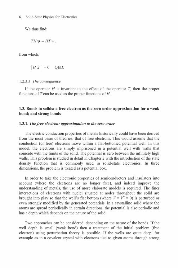
This approach involves improving the potential box model. This is done by the electrons interacting with a periodical internal potential generated by a crystal lattice (of Coulumbic potential varying 1/r with respect to the ions placed at nodes of the lattice). In Figure 1.1, we can see atoms periodically spaced a distance “a” apart. Each of the atoms has a radius denoted “R” (Figure 1.1a). A 1D representation of the potential energy of the electrons is given in Figure 1.1b. The condition a < 2R has been imposed.
Depending on the direction defined by the line Ox that joins the nuclei of the atoms, when an electron goes towards the nuclei, the potentials diverge. In fact, the study of the potential strictly in terms of Ox has no physical reality as the electrons here are conduction electrons in the external layers. According to the line (D) that does not traverse the nuclei, the electron-nuclei distance no longer reaches zero and potentials that tend towards finite values join together. In addition, the condition a < 2R decreases the barrier that is midway between adjacent nuclei by giving rise to a strong overlapping of potential curves. This results in a solid with a periodic, slightly fluctuating potential. The first representation of the potential as a flat-bottomed bowl (zero order approximation for the electrons) is now replaced with a periodically varying bowl. As a first approximation, and in one dimension (r x), the potential can be described as:
V(x) = w0 cos 2
.xa
The term w0, and the associated perturbation of the crystalline lattice, decrease in size as the relation a < 2R becomes increasingly valid. In practical terms, the smaller “a” is with respect to 2R, then the smaller the perturbation becomes, and the more justifiable the use of the perturbation method to treat the problem becomes. The corresponding approximation (first order approximation with the Hamiltonian perturbation being given by H(1) = w0 cos 2 )
ax is that of a semi-free electron and is
an improvement over that for the free electron (which ignores H(1)). The theory that results from this for the weak bond can equally be applied to the metallic bond, where there is an easily delocalized electron in a lattice with a low value of w0 (see Chapter 3).
8 Solid-State Physics for Electronics
Figure 1.1. Weak bonds and: (a) atomic orbitals (s orbitals with radius R) of a periodic lattice (period = a) respecting the condition a < 2R; (b) in 1D,
the resultant potential energy (thick line) seen by electrons
1.3.3. Strong bonds
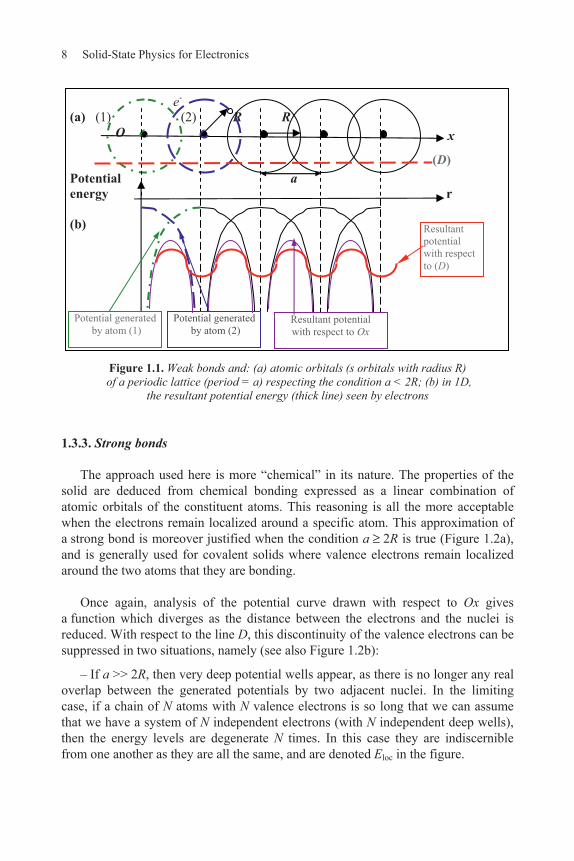
The approach used here is more “chemical” in its nature. The properties of the solid are deduced from chemical bonding expressed as a linear combination of atomic orbitals of the constituent atoms. This reasoning is all the more acceptable when the electrons remain localized around a specific atom. This approximation of a strong bond is moreover justified when the condition a 2R is true (Figure 1.2a), and is generally used for covalent solids where valence electrons remain localized around the two atoms that they are bonding.
Once again, analysis of the potential curve drawn with respect to Ox gives a function which diverges as the distance between the electrons and the nuclei is reduced. With respect to the line D, this discontinuity of the valence electrons can be suppressed in two situations, namely (see also Figure 1.2b):
– If a >> 2R, then very deep potential wells appear, as there is no longer any real overlap between the generated potentials by two adjacent nuclei. In the limiting case, if a chain of N atoms with N valence electrons is so long that we can assume that we have a system of N independent electrons (with N independent deep wells), then the energy levels are degenerate N times. In this case they are indiscernible from one another as they are all the same, and are denoted Eloc in the figure.
e- (a) (1) (2) R R O Potential a energy r (b)
Potential generated by atom (1)
Potential generated by atom (2)
Resultant potential with respect to (D)
Resultant potential with respect to Ox
(D)
x

Representations of Electron-Lattice Bonds 9
Figure 1.2. Strong bonds and: (a) atomic orbitals (s orbitals with radius R) in a periodic lattice (of period denoted a) where a 2R; (b) in 1D,
the resulting potential energy (thick curve) seen by electrons
– If a 2R, the closeness of neighboring atoms induces a slight overlap of nuclei generated potentials. This means that the potential wells are no longer independent and their degeneration is increased. Electrons from one bond can interact with those of another bond, giving rise to a spread in the band energy levels. It is worth noting that the resulting potential wells are nevertheless considerably deeper than those in weak bonds (where a < 2R), so that the electrons remain more localized around their base atom. Given these well depths, the perturbation method that was used for weak bonds is no longer viable. Instead, in order to treat this system we will have to turn to the Hückel method or use Floquet’s theorem (see Chapter 7).
1.3.4. Choosing between approximations for weak and strong bonds
The electrical behavior of metals is essentially determined by that of the conduction electrons. As detailed in section 1.3.2, these electrons are delocalized throughout the whole lattice and should be treated as weak bonds.
e-
(a) (1) (2) R
(D)
a Potential r energy (b)
Eloc Eloc Eloc
Potential generated by atom 1
Resultant potential with respect to Ox
Potential generated by atom 2
Resultant potential
with respect to D when
a 2R (strong bond)
Deep independent wells where Eloc level is degenerate
N times
R x
Potential wells with respect to D where
a >> 2R

10 Solid-State Physics for Electronics
Dielectrics (insulators), however, have electrons which are highly localized around one or two atoms. These materials can therefore only be described using strong-bond theory.
Semiconductors have carriers which are less localized. The external electrons can delocalize over the whole lattice, and can be thought of as semi-free. Thus, it can be more appropriate to use the strong-bond approximation for valence electrons from the internal layers, and the weak-bond approximation for conduction electrons.
1.4. Complementary material: basic evidence for the appearance of bands in solids
This section will be of use to those who have a basic understanding of wave mechanics or more notably experience in dealing with potential wells. For others, it is recommended that they read the complementary sections at the end of Chapters 2 and 3 beforehand.
This section shows how the bringing together of two atoms results in a splitting of the atoms’ energy levels. First, we associate each atom with a straight-walled potential well in which the electrons of each atom are localized. Second, we recall the solutions for the straight-walled potential wells, and then analyze their change as the atoms move closer to one another. It is then possible to imagine without difficulty the effect of moving N potential wells, together representing N atoms making up a solid.
1.4.1. Basic solutions for narrow potential wells
In Figure 1.3, we have W > 0, and this gives potential wells at intervals such that [– a /2, + a/2] where – W < 0.
We can thus state that ² ²
20,
mW and the energy E is the sum of kinetic
energy ² ² ²2 2
( )cp km m
E and potential energy.
As the related states are carry electrons then E < 0, and we can therefore write
that:
² ² ²² ² 0.
2 2cE W E k
m m
By making ² ² ²k > 0, is real.

Representations of Electron-Lattice Bonds 11
Schrödinger’s equation ² 2² ²
0d mdx
E V (where V is the potential energy
such that V = – W between –a/2 and a/2 but V = 0 outside of the well) can be written for the two regions:
2
2 22
22
2 – region I for x : 0,
2
so that 0
a d mE
dxd
dx
[1.8]
2
2 22
22
a 2– region II for – : ( ) 0,
2 2
so that 0.
a d mx E W
dxd
kdx
[1.9]
The solutions for equation [1.8] are (with the limiting conditions of (x) being finite when x ):
– for 2
: ( ) xI
ax x Ae
– for 2
: ( ) .xI
ax x Ae
The solution to equation [1.9] must be stationary because the potential wells are
narrow (which forbids propagation solutions). There are two types of solution:
– a symmetric solution in the form II ( ) cos ,x B kx for which the conditions of continuity with the solutions of region I give:
Figure 1.3. Straight potential wells of width a
Ep
0
– W
+ a/2 – a/2 x
Region II
Reg
ion
I
Reg
ion
I

12 Solid-State Physics for Electronics
2 2
2 2I II
I IIa a
x x
a a
x x
[1.10]
from which it can be deduced that 1
tan ,2
ka ka a
– an asymmetric solution in the form II ( ) sin .x B kx Just as before, the conditions of continuity make it possible to obtain the relationship written:
1 cotan .
2ka ka a [1.11]
Equations [1.10] and [1.11] can be combined in the form:
2tan .
² ²k
kak
[1.12]
In addition, equations [1.10] and [1.11] must be compatible with the equations that define and k, so that:
2² ² ² .
²mW
k [1.13]
ka
a
0 a 2 3
Figure 1.4. Solutions for narrow potential wells
Representations of Electron-Lattice Bonds 13
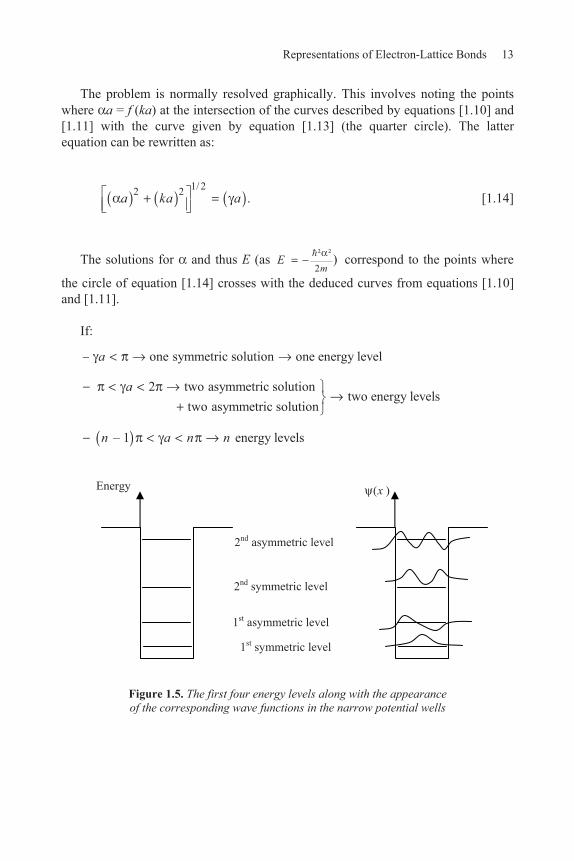
The problem is normally resolved graphically. This involves noting the points where a = f (ka) at the intersection of the curves described by equations [1.10] and [1.11] with the curve given by equation [1.13] (the quarter circle). The latter equation can be rewritten as:
1/ 22 2 .a ka a [1.14]
The solutions for and thus E (as ² ²2
)m
E correspond to the points where
the circle of equation [1.14] crosses with the deduced curves from equations [1.10] and [1.11].
If:
one symmetric solution one energy levela
2 two asymmetric solutiontwo energy levels
two asymmetric solutiona
– 1 energy levelsn a n n
Figure 1.5. The first four energy levels along with the appearance of the corresponding wave functions in the narrow potential wells
Energy
1st symmetric level
2nd symmetric level
2nd asymmetric level
1st asymmetric level
( )x

14 Solid-State Physics for Electronics
Figure 1.6. Scheme of the potential energies
of two narrow potential wells brought close to one another
1.4.2. Solutions for two neighboring narrow potential wells
Schrödinger’s equation, written for each of the regions denoted 1 to 5 in Figure 1.6 gives the following solutions (which can also be found in the problems later on in the book):
– Symmetric solution:
1
2
3
4
5
cos cos
.
x
x
Ce
B kx
A ch x
B kx
Ce
Conditions of continuity for x = d/2 and for x = d/2 + a/2 make it possible to state that:
2
2
tan ;
1 tan
dk
dk
ka th
k ka th [1.15]
– Similarly, for the asymmetric solution we obtain:
2
k 2
tan coth.
1 tan coth
dk
d
ka
k ka [1.16]
E
x – W
a d/2 d/2 d/2 a+d/2
(1) (2) (3) (4) (5)

Representations of Electron-Lattice Bonds 15
1.4.2.1. Neighboring potential wells that are well separated
If d is very large, equations [1.15] and [1.16] become:
k
tan
1+ tan k
ka
k ka [1.17]
and tend to give the same solutions as those obtained above for narrow wells. In effect, by making tan
k, equation [1.17] is then written as tan tan ka
for which the solution is 12
.ka n This in turn gives:
– if n is even then 2
tan ;kak
– if n is odd then 2
cotan .kak
In effect, we again find the solutions of equations [1.10] and [1.11] for isolated
wells, which is quite normal because when d is large the wells are isolated. Here though with a high value of d, the solution is degenerate as there are in effect two identical solutions, i.e. those of the isolated wells.
1.4.2.2. Closely placed neighboring wells
If d is small, we have 1de and:
2
2
tanh 1 2equations [1.15] and [1.16] give:
coth 1 2
d
d
d
d
e
e
- d1 - 2
- d1 - 2ek
e
tan
1+ tan ak
ka
k [1.18]
and - d1 + 2
- d1 + 2ek
e
1+ tan a k
tg a
k [1.19]

16 Solid-State Physics for Electronics
For the single solution ( 0) in equation [1.17] (if the wells are infinitely separated) there are now two solutions: one is s from equation [1.18] and the other is a from equation [1.19]. For isolated or well separated potential wells, all states (symmetric or asymmetric) are duplicated with two neighboring energy states (as s and a are in fact slightly different from 0). The difference in energy between the symmetric and asymmetric states tends towards zero as the two wells are separated ( ).d In addition, we can show quite clearly that the symmetric state is lower than the asymmetric state as in Figure 1.7.
Figure 1.7. Evolution of energy levels and electronic
states on going from one isolated well to two close wells
The example given shows how bringing together the discrete levels of the isolated atoms results in the creation of energy bands. The levels permitted in these bands are such that:
– two wells induce the formation of a “band” of two levels;
– n wells induce the formation of a “band” of n levels.
( )x
1st symm. 1st symm.
1st asymm.
1st asymm.
2nd asymm.
2nd symm.
isolated wells 2 wells in proximity

Chapter 2
The Free Electron and State Density Functions
2.1. Overview of the free electron
2.1.1. The model
As detailed in Chapter 1, the potential (V) (rigorously termed the potential energy) for a free electron (within the zero order approximation for solid-state electronics) is that of a flat-bottomed basin, as shown by the horizontal line in the 1D model of Figure 2.1. It can also be described by V = V0 = 0.
For a free electron placed in a potential V0 = 0 with an electronic state described by its proper function with energy and amplitude denoted by E0 and 0 , respectively, the Schrödinger equation for amplitude is:
0 0 020.
²m
E [2.1]
2.1.2. Parameters to be determined: state density functions in k or energy spaces
With:
02² = ,
²mE
k [2.2]

18 Solid-State Physics for Electronics
equation [2.1] can be written as:
0 0² 0.k [2.3]
Figure 2.1. (a) Symmetric wells of infinite depth (with the origin taken at the center of the wells); and (b) asymmetric wells with the origin taken at the well’s extremity
(when 0 < x < L, we have V(x) = 0 so that V(- x) = for a 1D model)
We shall now determine for different depth potential wells, with both symmetric and asymmetric forms, the corresponding solutions for the wave function ( 0) and the energy 0( ).E To each wave function there is a corresponding electronic state (characterized by quantum numbers). It is important in physical electronics to understand the way in which these states determine how energy levels are filled.
In solid-state physics, the state density function (also called the density of states) is particularly important. It can be calculated in the wave number (k) space or in the energies (E) space. In both cases, it is a function that is directly related to a dimension of space, so that it can be evaluated with respect to L = 1 (or V = L3 = 1 for a 3D system). In k space, the state density function [n(k)] is such that in one dimension n(k) dk represents the number of states placed in the interval dk (i.e. between k and k + dk in k wave number space). In 3D, n(k) d3k represents the number of states placed within the elementary volume d3k in k space.
Similarly, in terms of energy space, the state density function [Z(E)] is such that Z(E) dE represents the number of states that can be placed in the interval dE (i.e. inclusively between E and E + dE in energy space). The upshot is that if F(E) is the occupation probability of a level denoted E, then the number N(E) dE of electrons distributed in the energy space between E and E + dE is equal to N(E) dE = Z(E) F(E) dE.
V = V0 = 0
V(x)
L/2 – L/2 0
V V
V = V0 = 0
V(x)
L O
V V
x x

The Free Electron and State Density Functions 19
2.2. Study of the stationary regime of small scale (enabling the establishment of nodes at extremities) symmetric wells (1D model)
2.2.1. Preliminary remarks
For a symmetric well, as shown in Figure 2.1a, the Hamiltonian is such that H (x) = H(– x), because V(x) = V(– x) and ² ²
² ²d ddx d x
. If I denotes the inversion
operator, which changes x to – x, then
IH(x) = H(– x) = H(x).
H(x) being invariant with respect to I, the proper functions of I are also the proper functions of H (see Chapter 1). The form of the proper functions of I must be such that ( ) ( ).I x t x We can thus write: ( ) ( ) ( )I x t x x , and on multiplying the left-hand side by I, we now have:
2( ) ( ) ² ( )1, and 1
( ) ( )
I I x tI x t x t t .
I x x
The result is that
( ) ( ) ( )( ) ( ).
I x t x x x x (– x)
[2.4]
In these cases, the form of the solutions are either symmetric, as in ( ) ( )x x , or asymmetric, as in ( ) ( ).x x
2.2.2. Form of stationary wave functions for thin symmetric wells with width (L) equal to several inter-atomic distances ( L a ), associated with fixed boundary conditions (FBC)
0.2 2L L
[2.5]

20 Solid-State Physics for Electronics
This limiting condition is equivalent to the physical status of an electron that cannot leave the potential well due to it being infinitely high. The result is that between
2Lx and
2Lx = there is a zero probability of presence, hence the
preceding FBC:
02 2L L
.
The general stationary solution to equation [2.3] is:
0 ( ) cos sinx A kx + B kx.
The use of the boundary conditions of equation [2.5] means that:
0 cos + sin 02 2 2L L L
A k B k
or
0 cos sin 0.2 2 2L L L
A k B k
These last two equations result in the two same conditions:
– either A = 0 and 2
sin 0LB k , so that both 0 sinB kx and 2
kL n (n is
whole), so that 2L L
k n N where N is an even integer. The solution for
solution 0 is thus 0 sin NLN B x , with N being even; [2.6]
– or B = 0 and cos 0L2
A k , so that 0 cosA kx and 2 2
kL n (n is an
integer), so that 2 1L L
k n N where N is an odd integer. The solution for
0 is thus: 0 cos NLN A x , with N being odd. [2.7]

The Free Electron and State Density Functions 21
The normalization condition 0 ( )2/ 2
/ 2 1xNLL dx gives 2
LA B , and the
two solutions in equations [2.6] and [2.7] can be brought together in:
0 2sin
2NN L
xL L
, where N = 1, 2, 3, 4, etc. [2.8]
For both symmetric and asymmetric solutions, k is of the form
,Nk k NL
[2.9]
where N is an odd integer and the symmetric solution and is an even integer for the asymmetric solution. Thus, N takes on successive whole values i.e. 1, 2, 3, 4, etc. The value N = 0 is excluded as the corresponding function 0 0sin 0B k x has no physical significance (zero probability of presence). The integer values N' = – 1, – 2, – 3 (= – N) yield the same physical result, for the same probabilities as
0 0 02 2 2.N NN' Summing up, we can say that the only values worth
retaining are 1, 2, 3, 4, etc.N This quantification is restricted to the quantum number N without involving spin.
As we already know, spin makes it possible to differentiate between two electrons with the same quantum number N. This is due to a projection of kinetic moment on
the z axis which brings into play a new quantum number, namely 1
.2sm
We thus find that each N state can be filled by two electrons, one with a spin
1/ 2sm and wave function 0 ,N and the other with a spin 1/ 2sm and
wave function 0 .N
2.2.3. Study of energy
From equation [2.2] we deduce that: ² ²2
0 .km
E With k given by equation [2.9],
we find that the energy is quantified and takes on values given by:
22 Solid-State Physics for Electronics
20 ² ² ² ²
² ²,2 2 ² 8 ²
NN
k hE N N
m m L mL [2.10]
where N = 1, 2, 3, 4, etc.
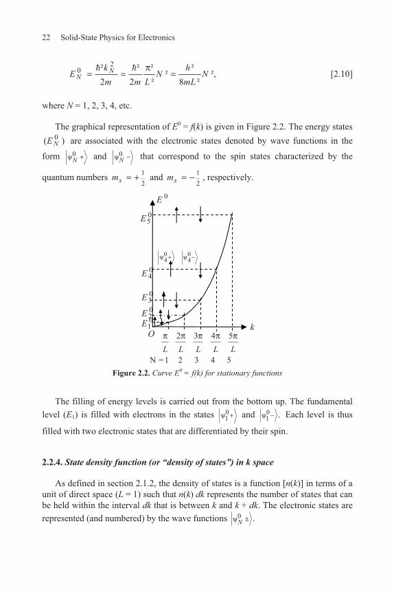
The graphical representation of E0 = f(k) is given in Figure 2.2. The energy states 0( )NE are associated with the electronic states denoted by wave functions in the
form 0N and 0
N that correspond to the spin states characterized by the
quantum numbers 12sm and 1
2sm , respectively.
Figure 2.2. Curve E0 = f(k) for stationary functions
The filling of energy levels is carried out from the bottom up. The fundamental level (E1) is filled with electrons in the states 0
1 and 01 . Each level is thus
filled with two electronic states that are differentiated by their spin.
2.2.4. State density function (or “density of states”) in k space
As defined in section 2.1.2, the density of states is a function [n(k)] in terms of a unit of direct space (L = 1) such that n(k) dk represents the number of states that can be held within the interval dk that is between k and k + dk. The electronic states are represented (and numbered) by the wave functions 0 .N
05E
2 3 4 5
N = 1 2 3 4 5
L L L L L
0 0 4 4
k O
03E
04E
02E01E
0E
The Free Electron and State Density Functions 23
On average, each interval of size L
dk can hold 1 orbital (without taking spin
into account). In fact, this interval corresponds to 2 orbital states; however, each is shared with the adjacent intervals. For example, in the interval 2 3,
L L we can place
the orbital states 02 and 0 ,3 but 0
2 is shared with 2 3,
L L and 2
, ,L L
just as
03 is shared with 2 3
,L L
and 3 4, .
L L From this we can see that the resulting
average is 1 orbital state per interval .L
dk
By taking spin into account, we can now place twice the number of states, so that in the interval
Ldk we now have two states. It is thus possible to write
( ) 2L
n k , so that with L = 1 (density function) we have:
2( ) .n k [2.11]
NOTE.– When dk = 1 we have n(k) dk = n(k), so that the state density function n(k) represents the number of states in a unit k space with the whole having a single unit dimension in direct space (L = 1).
2.3. Study of the stationary regime for asymmetric wells (1D model) with L a favoring the establishment of a stationary regime with nodes at extremities
The general solution for equation [2.3] is still 0 ( ) cos sinx A kx B kx, but the boundary conditions are now such that:
0 0(0) ( ) 0.L [2.12]
From the condition 0 (0) 0, we deduce that A = 0, from which 0 ( ) sin .x B kx
The condition 0( ) 0L thus gives sin 0B kL where kL = N , so that:
,Nk k NL
[2.13]

24 Solid-State Physics for Electronics
in which N = 1, 2, 3, 4, etc. noting that N < 0 does not change the probability of presence; in other terms it has no physical significance. We finally arrive at:
0 0( ) sin sin sin ( ).N NN
x B kx B k x B x xL
B can be determined using the normalization condition, as in: 0 ( )2
0 1xNL dx
that which gives 2L
B , from which
0 2( ) sin .N
Nx x
L L [2.14]
This solution (with N = 1, 2, 3, 4, etc.) replaces the solution for equation [2.8] for a symmetric system.
For its part, energy is still deduced from equation [2.2]. With the condition
imposed by equation [2.13] on kN, we are brought to the same expression as equation [2.10]:
0 0 2 01
² ² ² ²².
2 2 ²N NN
E E k E Nm m L
[2.15]
The representation of E0 = f (k) is also still given by Figure 2.4 and the state density function [n(k)] is the same as before, i.e. as in equation [2.11].
2.4. Solutions that favor propagation: wide potential wells where L 1 mm, i.e. several orders greater than inter-atomic distances
2.4.1. Wave function
This problem can be seen as that of a wire, or rather molecular wire, with a given length (L) tied around on itself as shown in Figure 2.3.
Figure 2.3. Molecular wire of length L
0 L x x + L

The Free Electron and State Density Functions 25
For a point with coordinate x, the probability is the same whatever the number of turns made, so we can write ( ) ( )x x L . Generally, after making n turns of length L we would end up at the same point, so we can write ( ) ( )x x nL where n is an integer. The boundary condition:
( ) ( )x x L [2.16]
is called the periodic boundary condition (PBC) or the Born-von Karman condition. When x = 0, it can be simplified so that:
(0) ( ).L [2.17]
That several revolutions are possible means that the solution must be a progressive wave. The amplitude of the free electrons wave function must take the form (see Chapter 1) given by:
0 0( ) ( ) .ikxkr x Ae [2.18]
In effect, with the form of the wave being that presented in section 1.2.2, the function ( , )r t here becomes the propagation wave 0 ( )( , ) ,i kx tx t Ae which propagates towards x > 0 as k > 0. As propagation in the opposite sense is possible, we find that k < 0 is therefore also physically possible.
The normalization condition 2
0 ( ) 1Lk x dx makes it possible to determine
1 .L
A For its part the condition expressed in equation [2.17] gives 0 ,ik ikLe e
so that 1 ,ikLe from which kL = 2N , which in turn means that:
2Nk k N
L, where N = 0, ± 1, ± 2, ± 3, ± 4.... [2.19]
(the solution for N = 0 simply gives a probability for a constant presence).
Placing these results into equation [2.18] we finally have for the amplitude function:
20 0 1
( ) ( ) .N
N
i NxLik x
N kr x Ae eL
[2.20]

26 Solid-State Physics for Electronics
NOTE.– We can immediately say that for the conditions that favor propagation, we
now have 102
00 ( ) ² ,N k LNkN
x Ak a constant value wherever along (x)
an electron might be. The electrons move freely, without any specific localization (i.e. the probability of their presence is constant, whatever the value of x).
2.4.2. Study of energy
By taking the expression for k given in equation [2.19] and placing it into equation [2.2], we obtain:
220 0 ² 2
2NE E Nm L
, with N = ± 1, ± 2, ± 3, ± 4.... [2.21]
Figure 2.4. Curve of E0 = f(k)
for progressive solutions
0 ( )NE f k is represented in Figure 2.4. Without taking spin into account, at each electronic level there are two electronic states (associated with the two possible values of N, as in N N ). Including spin, each level actually corresponds to
02E
2 4 6
1 2 3
L L L
N =
0 03 3
k 6 4 2
3 2 1
– – – L L L
– – –
0 03 3
E0
O
01E
03E

The Free Electron and State Density Functions 27
four states. To put it another way, we can state that each point on the curve corresponding to either a negative or a positive value of N is associated with two states (up and down spin).
When taking spin into account, we also find that the degree of degeneracy is four as each energy level can accommodate four electrons, each corresponding to a specific wave function. Thus, at the Nth level these four functions are:
0 ,N 0 ,N 0 ,N 0 .N
2.4.3. Study of the state density function in k space
Taking electron spin into account, we can now place on average two electrons into the interval 2
Ldk . There are four electrons in all, but with two in each
division. Thus, 2( ) 2L
n k , so that with L = 1:
1( ) .n k [2.22]
To conclude, we can see that with progressive solutions, the number of states that can be placed in a unit interval in reciprocal space is equal to 1/ . One half of that can be placed in stationary solutions, even though the available k space is twice as large. It should be noted that the negative values of N and thus of k must also be taken into account.
2.5. State density function represented in energy space for free electrons in a 1D system
The curves given by E = f (k) give a direct relation between k and energy spaces. In the space that we have defined, as detailed in section 2.1.2, the Z(E) state density function is such that Z(E) dE represents the number of energy states between E and E + dE with respect to a material unit dimension (in 1D, L = 1 unit length).
Rigorously speaking, Z(E) should be a discontinuous function as it is defined, a priori, only for discrete values of energy corresponding to the solution of the

28 Solid-State Physics for Electronics
Schrödinger equations [2.10] and [2.15] or [2.21] as below, respectively for stationary or progressive cases:
20 ² ² 4 ² ²
² ².2 2 ² 2 ²
NN
k hE N N
m m L mL [2.21]
A numerical estimation can be carried out to find the typical value for free (conduction) electrons and, in this example, shows that EF 3 eV (Fermi energy measured with respect to the bottom of the potential wells).
By making L = 1 mm (which is small enough to be at the scale typically used for lab samples, and large enough to contain a sufficiently high enough number of particles to give a statistical average), equation [2.18] gives N 1.5 × 10⁶.
The difference in energy between two adjacent states [N + 1] and N is thus given by:
2 2
1 2 2(2 1) ,2
N Nh h
E E E N NmL mL
giving E 4 × 10⁻⁶ eV. This holds where EF is small and in effect the conduction electrons show
a discrete energy value that can be neglected in an overall representation of electron energies (see below).
To conclude, the energy levels are quantified but the difference in their energies are so small that the function Z(E) as defined above can be considered as being quasi-continuous around EF. Often the term quasi-continuum is used in this situation.
Energy EF 3 eV
E 2 eV 1 eV 0

The Free Electron and State Density Functions 29
2.5.1. Stationary solution for FBC
Here, as shown in Figure 2.2, only values with k > 0 are physically relevant. 01E
pertains to a single value (k1) in k space. Similarly, 02E corresponds to a single value
(k2). A consequence of this relationship between energy and k spaces is that for a number of states with energies between E and E + dE there is a corresponding and equal number of states between k and k + dk. This can be written as:
Z(E) dE = n(k) dk. [2.23]
From this it can be deduced that ( )( ) .n kdEdk
Z E
With E from equation [2.2], i.e. ²2
²,m
E k we also equally have 2mEk
and thus ² ² 2 22
1/ 2 1/ 22 .dE mEdk m m m
k E
From this it can be deduced that, for n(k) given by equation [2.11] (or rather
2( ) )n k :
1 2( ) .
mZ E
E [2.24]
Thus, when E increases, Z(E) decreases, as shown in Figure 2.5.
Z(E)
E
Z(E) dE
E E + dE
Z(E)
Figure 2.5. State density function for a stationary or progressive 1D system

30 Solid-State Physics for Electronics
2.5.2. Progressive solutions for progressive boundary conditions (PBC)
As shown in Figures 2.4 and 2.6, here the interval dE corresponds simultaneously to the intervals dk+ (for k > 0) and dk – (for k < 0).
As in both dk+ and dk– we can place the same number of states, it is possible to state that:
( ) ( ) ( ) 2 ( ) .Z E dE n k dk n k dk n k dk
Thus, ( )( ) 2 .n kdEdk
Z E
With n (k) given by equation [2.22], 1( )n k , we obtain: 2 1( ) ,dEdk
Z E
where dEdk
was calculated in the preceding section.
We again find the same expression for Z(E), as shown in equation [2.24] and thus the same graphical representation as shown in Figure 2.5.
2.5.3. Conclusion: comparing the number of calculated states for FBC and PBC
Stationary waves: FBC
0 ² ²²
2 ²NE Nm L
Figure 2.6. Plot of E = f(k) for progressive solutions
k-2 k-1 k+1 k+2
E
k
dk+dk –
dE

The Free Electron and State Density Functions 31
2( )n k
Progressive waves: PBC
20 ² 2
²2NE Nm L
1( )n k
Figure 2.7. FBC and PBC states
2 3 4
1 2 3 4
L L L L
N
k O
03E
04
² ²4²
2 ²E
m L
02E 01E
0E
4 2 2 4
2 – 1 1 2
– – L L L L
– N – N
k O
202
² 22²
2E
m L
01E
0E

32 Solid-State Physics for Electronics
The total number of states calculated over all the reciprocal space is in fact the same for the two types of solution, as with the FBC there is the involvement of only one half-space and n(k) = 2/ , while under PBC both half-spaces are brought in (i.e. k > 0 and k < 0) and n(k) = 1/ . It can be seen in Figure 2.7 that there are eight states represented when taking into account spin for the two cases (four states not accounting for spin associated with the points on the plots in Figure 2.7) with:
– k varying from 0 to 4 /L or from 0 to 4 /L;
– E varying from 0 to 2 2 2 20 0
4 222 2
22 24 2 .E Em m LLFBC PBC
2.6. From electrons in a 3D system (potential box)
2.6.1. Form of the wave functions
Figure 2.8. A parallelepiped box (direct space)
We assume that the free electrons are closed within a parallelepiped box with sides of length L1, L2, L3 as shown in Figure 2.8. The potential is zero inside the box and infinite outside. The Schrödinger equation is thus given by:
0 0 02( , , ) ( , , ) 0.
²m
x y z E x y z
By making 2²
0² ,mk E it can be rewritten as: 0 0² 0.k
L1
L2
L3
O
x
y
z

The Free Electron and State Density Functions 33
The resolution of this equation can be carried out after separating the variables. In order to do this, we make: 0 0 0 0
1 2 3( , , ) ( ) ( ) ( )x y z x y z and 0 01E E
0 02 3E E . From this we can deduce three equations with the same form:
a) 2 0 ( ) 2 21
2 2 20 0 01 1 1( ) 0, so that on making
d x m m
dx
2xE x k E we have:
02 01
1² ( )
( ) 0² x
d xk x
dx
b) 2 0 ( ) 2 22
2 2 20 0 02 2 2( ) 0, so that on making
d y m m
dy
2yE y k E we have:
02 02
2² ( )
( ) 0² y
d yk y
dy
c) 2 0 ( ) 2 23
2 2 20 0 03 3 3( ) 0, so by making
d z m m
dz
2zE z k E we have:
02 03
3² ( )
( ) 0² z
d zk z
dz
2.6.1.1. Case favoring fixed boundary conditions
Here the FBCs are:
– with respect to Ox: 0 01 1 1(0) ( ) 0,L
– with respect to Oy: 0 02 2 2(0) ( ) 0,L
– with respect to Oz: 0 03 3 3(0) ( ) 0.L

34 Solid-State Physics for Electronics
The use of these boundary limits means that we can solve these differential equations directly from the equivalent 1D system (the boundary limits are identical to those in the 1D system with an origin at an extremity – see section 2.3):
0 0 0 0 0
1 2 3
( , , ) ( , , ) ( ) ( ) ( )
sin sin sin ,
x y zn n n n
yx x
x y z x y z x y z
nn nA x y z
L L L
[2.25]
where 1 2 3
, , L L Lx x y y z zk n k n k n and nx, ny and nz are positive integers.
Energy is given by:
0 0 0 0 2 2 21 2 3
2 2 22 2 21 2 3
²2
² ² ² ².
2
x y z
x y z
E E E E k k km
n n nm L L L
[2.26]
2.6.1.2. Case favoring progressive boundary conditions
Analogously to the case for limiting conditions, we have:
– with respect to Ox: 0 01 1 1( ) ( ),x x L
– with respect to Oy: 0 02 2 2( ) ( ),y y L
– with respect to Oz: 0 03 3 3( ) ( ).z z L
The use of these boundary limits means that we can solve these differential
equations directly from the equivalent 1D system (the boundary limits are identical to those in the 1D system where propagation is favored – see section 2.4.1):
22 2
31 2
0 0 0 0 0
1 2 3
( ) ( , , )
=
x y z
yx z
i n zi n x i n y zx y LL L
n k k k k
ik yik x ik zx y z
r x y z
A A A e e e Ae e e
[2.27]

The Free Electron and State Density Functions 35
in which 1 2 3x y zA A A A , 2 2 2
1 2 3, ,
L L Lx x y y z zk n k n k n and where nx,
ny and nz are positive or negative integers. Energy is given by:
22 20 0 0 0 2 2 2
1 2 3 2 2 21 2 3
² ².
2 2yx z
x y znh n n
E E E E k k km m L L L
[2.28]
2.6.2. Expression for the state density functions in k space
2.6.2.1. Where stationary solutions are favored
In 3D, we can divide the k space into elemental cells (nx, ny, nz, which change values as integers) such that their smallest variation is given by nx = ny = nz = 1 and that the sides of the smallest, elemental cell are given by
1,
Lxk
2,
Lyk3
.Lzk The elemental cells are such that their nodes (upmost point)
are associated with an electronic state represented by a wave function given by:
0 0
0 0 0
1 2 3
( , , ) ( , , )
sin sin sin .x y z
n
yx xk k k
x y z x y z
nn nA x y z
L L L
Each elemental cell thus has eight nodes, each of which corresponds to eight states that are, in turn, each shared across eight elemental cells. Without taking spin into account, we can assert that 8
81 state per cell on average. Taking spin states
into account we can now place two electronic states into each elemental cell.
The elemental cells have an elemental volume given by:
33
1 2 3 ,x y zk k k k
L L L V

36 Solid-State Physics for Electronics
where V is the volume in direct space (starting with a parallelepiped, see Figure 2.8). For a unit volume in direct space (V = 1 given for the calculation of the state density function), we have 3 3
1.k
V
Still using n(k) to denote the state density function, we can write that
3 1
( ) 2V
n k k , so that 3( ) 2n k . In other words,
32
( ) .n k [2.29]
2.6.2.2. Where progressive solutions are favored
In 3D, we have 2 2 2
1 2 3, , ,
L L Lx y zk k k and the elemental cells are
such that each has a node associated with an electronic state represented by a wave function in the form:
22 2
31 20 0 0 0( ) .x y z
i n zi n x i n y zx y LL Ln k k kr Ae e e
The elemental cells thus have an elemental volume given by:
33
1 2 3
2 2 2 8 x y zk k k k
L L L V
where V is the direct space volume. For a direct space unit volume (V = 1), we have 3 3
18 ,
Vk and then by using n(k) to denote the state density function, we
can write that 3 1
( ) 2,V
n k k so that 3( )8 2,n k which in other words
means:
31
( ) .4
n k [2.30]

The Free Electron and State Density Functions 37
2.6.3. Expression for the state density functions in k space
2.6.3.1. Where stationary solutions are favored
The calculation for the state density function now denoted Z(E) can be carried out using two different routes:
– using the correlation between k and energy spaces;
– via a direct calculation in energy space using quantum numbers.
Here we will use the direct method.
First we can note that with stationary solutions where quantum numbers nx, ny and nz are positive, the quantum number space must be held within the first octet (nx, ny, nz > 0) as shown in Figure 2.8a. If the problem is dealt with in 2D only, then the space (or more exactly the plain) should be within the first quadrant, as indicated in Figure 2.8b.
Figure 2.8. Nodes and states in quantum number space:
(a) 3D space with nx, ny, and nz as whole integers; (b) likewise in 2D
In quantum number space, just as in k space, the cells and their nodes are associated with electronic states that are characterized by their electronic wave functions, as in , ,n n nx y z where each is denoted with respect to its specific
quantum number nx, ny, and nz. Once we take spin into account, characterized by the
ny
2,3
3
2 1
0 1 2 3 4 nx
2,1,1
ny
nx
nz
1,1,1 1, 1, 1x y zn n n
2,2,2
(a) (b)

38 Solid-State Physics for Electronics
quantum numbers 12sm and 1
2,sm these functions in fact give rise to the
electronic states , ,n n nx y z and n ,n ,nx y z .
From equation [2.23], we can see that the states of the equi-energy E = constant
are spread out over a sphere of radius given by n = constant 8 ²²
.mLE
h Also, in the
quantum number space shown in Figure 2.9, the state that have energies between E and E + dE are spread between the spheres of radius n and n + dn such that
8 ²²
mLE
hn and 8 ²
( )²
.mLE dE
hn dn This gives a volume which is equal to
4 n²dn. With the quantum numbers being obligatorily positive we have restricted the quantum number space to the first octant (where nx, ny, nz > 0) in which the preceding volume (divided by eight) is reduced to 4 ² ²
8 2.n dn n dn
Figure 2.9. The relation between the quantum number and energy spaces
The number of cells that can be placed in this volume is given simply by ²2
n dn
when the cells have a volume given by 31 1x y zn n n (the quantum number can vary in single steps in each particular direction, as in Figure 2.8). Without taking spin into account, each cell contains eight states, but each state is shared between eight cells, so that on average we can therefore place one state in each cell. So, again without taking spin into account, the number of electronic states that can be placed is thus ²
2.n dn
nz
ny nx
n+dn E + dE
n E

The Free Electron and State Density Functions 39
Taking spin into account means that we can now place twice the number of states, so that the total number of electronic states is equal to n²dn. We can thus finally write that:
( ) ² .Z E dE n dn
With equation [2.26] (where 2 2 2² x y zn n n n and it is supposed that L1 = L2 = L3 = 1 so as to have a unit volume from which the density functions can be obtained) which takes the form of ² ²
8 ² 8² ²,h h
mL mE n n we have ²
4,h
mdE ndn
from which 4²
.mh
dE ndn
The result in that: 48²²
² ( ) ,mmE
hhn dn dE Z E dE so that:
3 / 2
34 (2 )
( ) .m
Z E Eh
[2.31]
The curve thus has a parabolic shape, as shown in Figure 2.10.
Z(E)
E
Z(E+dE) Z(E)
Z(E)dE
E + dE
Figure 2.10. State density function in 3D

40 Solid-State Physics for Electronics
NOTE.– If we use the correlation between k space and energy space, we can write:
2( ) 33 4 ² 1
( ) ( ) ( ) ² .8 8 ²
n kD
kdV k dkZ E dE n k n k k dk
With 2² mEk we have on one side 2mEk , and on the other 2 ,mkdk dE from which we once again obtain equation [2.28].
2.6.3.2. Problem: where progressive solutions are favored (see also problems 5 and 6 of this chapter)
In this case, nx, ny, and nz are positive or negative integers and the quantum number spaces – just as that for k – is no longer restricted to the first octet but covers all space.
By using the correlation between k space and energy space, we can thus write:
1( ) 343 1
( ) ( ) ( )4 ² ² ,²
n kD
kZ E dE n k dV n k k dk k dk
from which we again find equation [2.31].
2.7. Problems
The reader is advised that if he or she has not yet looked at the basics of statistical thermodynamics, including the use and significance of the Fermi-Dirac function, problems 1, 3 and 4 should be attempted after reading section 4.4.3.2 of this book.

The Free Electron and State Density Functions 41
2.7.1. Problem 1: the function Z(E) in 1D
Here we are looking at free electrons in a small one-dimensioned medium with L being equal to several nanometers. The total number of electrons is equal to Nt and the filling of the energy levels at absolute zero is under consideration.
1) What type of boundary conditions should we use?
2) Give the value of N of the last occupied level.
3)
a) If EF(0) EF represents the energy of the highest fully occupied level, express the value of EF as a function of Nt.
b) From this and as a function of EF, deduce the expression of the total numbers of orbitals [N(EF)] (of electronic states including spin) for electrons with energies lower than EF.
4)
a) Generalize the last expression for any level E that is lower than EF.
b) From this deduce the expression for the function [Z(E)] of the density of energy states.
Answers
1) The medium is of a sufficiently small size so that we can assume that there is a stationary regime and as a consequence the use of fixed boundary conditions, which takes into account the presence of a node at each extremity of the system.
2) Being at absolute zero, the levels are filled as a continuum from the lowest level N = 1 to the highest. With two electrons placed into each level (each electron has a different spin), the highest level can thus be discerned using
2.NtN
3)
a) We can now write that 10 ² ²
2 ² 2
2
2t
N tm LF N N NE E ²
2 2
2.Nt
m L
b) We thus have N(EF) = Nt, so that by taking the preceding equation into account, we now have:
1 21/ 22 ²
( ) .2F F
LN E E
m

42 Solid-State Physics for Electronics
4)
a) For any level E which is such that E < EF, the preceding relationship retains its validity when the level EF is replaced by the level E (which accords to the same filling rules as the level EF). The total number of electronic states with energy less than E, including spin states and denoted N(E) is thus given by:
1 21/ 22 ²
( )2
LN E E
m
b) The function Z(E) is such that [dN(E)]L = 1 = Z(E) dE (number of states with energies comprised between E and E = dE for a crystal with a unit dimension, i.e. L = 1), so that:
1/ 21/ 21/ 2 1/ 2
1 1
( ) ² 1( ) 2 .
2L L
dN E LZ E E m E
dE m
Here we return to the expression given in equation [2.24] and plotted in Figure 2.5.
2.7.2. Problem 2: diffusion length at the metal-vacuum interface
The electronic representation of a metal using potential bowls with flat bottoms makes it possible to define the work function (Ws) (of electrons) of the metal. The origin of the potentials was taken as being the level of electrons in a vacuum at an infinite distance from the metal with the highest energy level (last occupied level) being in the metal (at absolute zero temperature) and situated at – Ws. The work function is thus equal to W = 0 – (– Ws) = Ws (where Ws is positive).
This level corresponds to the Fermi level EF, which is generally defined with respect to the last occupied band (see also section 1.3 in [MOL 06]).
The potential bowl is thus represented in the following diagram, and it is noticeable that it no longer resembles the infinitely high potential wells. The depth of the wells being finite means that the electrons situated at the Fermi level can now “penetrate” the vacuum.

The Free Electron and State Density Functions 43
For a value Ws = 3 eV, evaluate for x > 0 the penetration length Lx (of diffusion)
into the vacuum for electrons at the Fermi level of the metal (divided by e for the wave function following the pathway Lx).
Answer For electrons that are likely to be in the zone x > 0 where V = 0 with an energy
corresponding to that of the level EF = – Ws, we have 0V
sE V E W . The
Schrödinger equation ² 2² ²
( ) 0d mdx
E V can thus be written for these
electrons as:
² 20.
² ² sd m
Wdx
By making 2²
² msk W (with Ws > 0), the solution is ( ) .kx kxx Ae Be
When x > 0, the boundary condition ( ) 0 imposes A = 0, so that
( ) .kxx Be
The diffusion length Lx is defined by ( )x
Lxx e , which is such that ( ) 1(0)Lx
e (divided by e for the wave function following the pathway Lx), and we
now have: 12k mWs
xL .
Numerically speaking, with m = 0.9 × 10 30 kg, Ws = 3 eV = 3 × 1.6 × 10 19 J and with 1Js, we obtain Lx 10 10 m = 0.1 nm.
Level of the vacuum Energy
EF
Ws
Ws x 0 Lx
(0)/e
0

44 Solid-State Physics for Electronics
2.7.3. Problem 3: 2D media: state density function and the behavior of the Fermi energy as a function of temperature for a metallic state
This section considers a square 2D metal in the Oxy plane with N atoms distributed with spatial periodicity with respect to both Ox and Oy. The sides of the crystal are denoted Lx and Ly and are such that Lx = Ly = L = (N + 1) a Na as N is very large (N >> 1). The mono-valent atoms placed at the lattice nodes each liberate a free electron, which are thus present in numbers given by Nt = N², to which there is a corresponding electronic density given by ²
² ²N NtL LeN .
1) For the reciprocal space (k space) indicate:
a) The dimension of an elementary cell.
b) The form of the equi-energy curve.
c) Which surface the electrons are placed on that have energy less than or equal to a given value of E.
d) The maximum number of electrons that can be held in a unit surface.
e) The maximum number N' of electrons with energies less than or equal to a given E, where N' = f [N, a, m, E].
2)
a) Determine the expression of the energy states density function (Z(E) = g[m, E]), and conclude.
b) Calculate the Fermi energy at absolute zero EF(0) defined by EF(0) = Emaximum for T = 0 K. What is the relation that exists between EF(0) and Z(E)?
c) Numerical application: using a = 0.3 nm, calculate the value of EF(0).
d) Given that the integration is 1
0
1 ²...
1 6 ²
1
10
0E
E
pE dE pp
e
pE , obtained
from 0 ( ) ( )eN Z E f E dE , where f (E) is the Fermi-Dirac function given by
( )
1
1 exp( )
E E TF
kT
f E (see section 4.4.3.2 if needed), show that the Fermi energy
EF(T) for a 2D crystal is strictly independent of the temperature as in EF(T) = EF.

The Free Electron and State Density Functions 45
Answers
1)
a) We have 2 2 2 22 2( ) ( ) .L L Lx y
k kx ky k
b) The energy of free electrons is given by ² ²2
km
E . In the k space, where
2²
,mEk the energy is constant for 2²
mEk constant (equation for a circle
of radius 2²
mER k ). The cells distributed around the circle contain electrons
with a given equi-energy E.
c) Electrons with energies lower than a given value E are thus spread around
the inside of the circle surface with a radius 2²
mEk constant, and surface
value 2²
² .mEk
d) In a unit surface, the number of surface cells 2 2
Lthat we can place are
such that: 2 2
2
21
.
L
L The maximum umber of electrons that can thus be placed
are (with two electrons per cell) 2
22 .Lx
e) Electrons with energies less than E are distributed on the inside of the circle
of radius 2²
mEk and of surface 2²
² .mEk On this surface, we can thus
distribute a maximum number of electrons equal to:
N' =2
22L
x2
²mE
x4 ² 4 ² ²
.² ²
mL mN aE E
h h
It should be noted that in order to attain the maximum number, the probability that each cell can be occupied by two electrons should be equal to unity.

46 Solid-State Physics for Electronics
2)
a) On taking spin into account, each state corresponds to an electron (non-degenerate problem). Thus, the maximum number N' of electrons with energies less than E is equal to the total number of states existing between 0 and the energy E.
The state density Z(E) is such that the number per unit surface N'/L² of energy states below E are in accordance with: '
² 0 ( ) ,NL
E Z E dE from which
'/ ²( ) d N L
dEZ E , so that 4
² ²( ) m m
hZ E constant.
The function Z(E) is thus a straight line in 2D space.
b) When E = EF(0), all states below EF(0) are occupied by Nt = N² electrons of the system, and therefore (0)' ²
FtE EN N N . Given the expression
obtained in Question 1(e) for E = EF(0), we thus have:
(0)4 ² ²
' (0) ²,²F
FE EmN a
N E Nh
from which:
² ² ²(0)
4 ² ² ² ( )Fh N
Ema ma L Z E
.
c) Numerical application. With a = 0.3 nm, we obtain EF(0) = 2.7 eV.
d) With ²² (0)
( ) NL EF
Z E , we can thus write:
Z(E)
E
Constant

The Free Electron and State Density Functions 47
0 0
² ²( ) ( ) ( ) ,
² ² (0)eF
N NN Z E f E dE f E dE
L L E
from which 0(0) ( ) ,FE f E dE so that:
( )1
( )
0,
0
1(0) ( ) 1 0 ( ).
1
F
E T EFkT E TF
p E kT
F F FE dE E T E T
e
2.7.4. Problem 4: Fermi energy of a 3D conductor
Show that the Fermi energy EF(T) of a 3D conductor described by a free electrons model is practically independent of temperature. In order to do this, consider that the total effective number of free electrons in a 3D conductor is Ne.
1) For any given temperature T, determine the relation Ne = f (EF(T)) by using, just as for the 2D conductor, the fact that 0 ( ) ( )eN Z E f E dE , with
1( )
1 exp( )
E E TFkT
f E and 1 ²1 6 ²
101
10
0... .
p pE dEpE
Ee
pE
2) For T = 0 K, find the relation Ne = g(EF0) with EF0 = (EF)T =0 K.
3) Express EF as a function of EF0. Conclude, knowing that the value of the Fermi level for a metal is often of the order of 3 eV.
Answers
1) We have 0 ( ) ( )eN Z E f E dE , so that with 3 / 24 (2 )
3( ) m
hZ E E (from
equation [2.28] for the 3D model) we can write ( ) cZ E A E with 3 / 24 (2 )
3m
hcA . Hence, we can write:

48 Solid-State Physics for Electronics
1/ 2( ) /
( ) ( )1
( )
1/ 2 1/ 2
0 0
3 / 2
c 2
1 1
2 ² 1 ² ² A ( ) ... .
3 6 2 ( )
F
pE T kT
E E TF E T EFkT kT E TF
e c c
FF
E EN A dE A dE
e e
k TE T
E T
2) At absolute zero, the number of electrons is unchanged. The levels are simply filled up to the Fermi level with an occupation probability of 100%. Using EF0 to denote the Fermi level at absolute zero, we can write that:
0 0 1/ 2 3/ 20
0 0
2( ) .
3
F FE E
e c c FN Z E dE A E dE A E
3) Using the equations for Ne obtained in response to questions 1) and 2), and equating them, we obtain:
3/ 2 3/ 202
2 ² 1 ² ² 2( ) ...
3 6 2 3( )F F
F
k TE T E
E T,
from which
2 / 3
0 02 2
2
00
² ² ² ² ² ²( ) 1 ... 1 ...
8 12( ) ( )
² 1 ... .
12
F F FF F
FF
k T k TE T E E
E T E T
kTE
E
In terms of numbers, when EF0 EF(T) 3 eV, T = 300 K (so that k = 8.6 × 10⁻⁵ eVK-1 and kT 2.6 × 10⁻² eV), and the corrective term required is:
222 25
05.8 10 eV.
12 ( ) 12F F
kT kTE T E

The Free Electron and State Density Functions 49
The value of the corrective term is negligible with respect to the 3 eV of the metal Fermi level. We can thus assume that the position of the Fermi level is practically independent of temperature, at least within reach of ambient temperatures.
2.7.5. Problem 5: establishing the state density function via reasoning in moment or k spaces
Derive the aforementioned equation for the state density function in 3D but this time by:
1) using the space of moments (p) wherein Hesienberg’s relation can be written with respect to a specific direction, for example x so that ;xx p h and
2) in k space where the use of Heisenberg’s relation can be made and justified.
Answers
1) In 3D, Heisenberg’s equation is written: 3,x y zx y z p p p h so that by making V x y z (space within which the particle can move) we have:
3
.x y zh
p p pV
A free electron placed in a potential of zero exhibits a relation between E and p that is: ²
2.p
mE Quantum states for energies between E and E + dE in moment
space are situated between spheres with radii p ( 2mE ) and p + dp. The volume between two spheres is 4 ² .p dp This volume can hold a number of cells of volume
p3 = px py pz given by 4 ²3 /
.p dp
h V
By making V = 1 (to obtain a given density) and recognizing that we can place
two electrons per cell, the state density function Z(E) is such that 4 ²
3( ) 2 .p dp
hZ E dE The differentiation of ² 2p mE gives 2 2 ,pdp mdE
from which 3/ 2 1/ 22 ² 2 ,p dp m E dE and we directly obtain:
3 / 21/ 2
22
( ) 4 .m
Z E dE E dEh
50 Solid-State Physics for Electronics
2) With p k , we have x xp k , from which 2xx k
(Heisenberg’s other equation!). From this we deduce that 32
.Vx y zk k k
This relation is identical to that deduced for the quantification with progressive boundary conditions (PBC), where for a free electron we have ( ) xik x
k x Ae
( ) ,x x Likk x L Ae from which 1,xik Le so that 2 ( ),xk L n so that
between adjacent values of n, kx varies by 2 .Lxk This result makes it possible
to justify Heisenberg’s equation, as L is the space x in which the electron can probably be found.
In k space, the volume for energies between E and E + dE is situated between the spheres of radii k ( 2mE ) and k + dk, equal to a volume of 4 k²dk. Into this
volume we can place 4 ²3(8 ) /
k dk
Vcells, so that to obtain the state density function when
V = 1, we have ²²
( ) k dkZ E dE electrons. With 2²
² ,mEk we can state that
²
,m dEkdk and we once again obtain:
3 / 21/ 2
22
( ) 4 .m
Z E dE E dEh
2.7.6. Problem 6: general equations for the state density functions expressed in reciprocal (k) space or in energy space
1) Based on the reasoning given in problem 5 question 2, show how it is possible to write the 3D relation between the state density function in energy [Z(E)] and the state density function in k space [n(k)] in the form:
3
( )( ) ( ) ,
V EZ E dE n k d k detailing the significance of ( ).V E
2) For theories more refined than that based on the free electron, the dispersion equation for E(k) can be quite complex, making the determination of ( )V E more

The Free Electron and State Density Functions 51
difficult. Show how the following general equation for 3D space can be derived and detail the significance of S(E).
3( )
1( ) .
4 S E k
dSZ E
grad E
3) What happens to the preceding equation in 2D? Apply it to free electrons to obtain the equation for Z(E) as found in question 2 of the preceding problem 3.
Answers
1) By definition, the density function of energy states Z(E) is such that the number of states with energies between E and E + dE is given by Z(E)dE. For free
electrons (where ² ²2
,km
E so that 2 ),mEk the corresponding energy volume
is situated in k space between two spheres of radii k and k + dk, that is, of volume dVk = 4 k²dk. The transition from the function n(k), i.e. the state density in k space k, to the function Z(E) – the density of state in energy space – is thus given via the equation:
( ) ( )4 ² .Z E dE n k k dk
Given that 134
( )n k (see equation [2.27]), we once again find the equation in
problem 5, i.e. ²²
( ) .k dkZ E dE
For free electrons, as n(k) is a constant in k space (equation [2.27]) we can thus
write that 3( )( ) ( ) V EZ E dE n k d k where 3
( ) 4 ² .V E d k k dk
( )V E thus represents the volume of reciprocal space between the surface S(E)
of the equi-energy E and the surface S(E + dE) of the equi-energy E + dE. In more general terms, if n(k) varies with k, the preceding relationship should
thus be written as:
3
( )( ) ( ) .
V EZ E dE n k d k

52 Solid-State Physics for Electronics
2) The elemental volume 3d k can be seen as the product of elemental surface d2S carried through area S(E), in other words the surface of the equi-energy E in reciprocal space through the space between areas S(E) and S(E + dE) along a line normal to S(E). This normal S(E) is collinear to gradk E so that we can state that:
3 2 2grad .gradE
k
dEd k d S k dE d S
E
Placing this in 3( )( ) ( )V EZ E dE n k d k where 1
34( )n k (equation
independent from the dispersion equation), we have ( )Z E dE 21
3 grad4 ( ) ,d S
EkV E dE from which:
2
3( )
1( )
4 S E k
d SZ E
grad E
where S(E) is the surface of the equi-energy E in reciprocal space.
NOTE.– We can quickly verify the veracity of equation [2.28] for free electrons. Here, in effect we find:
( ² ² / 2 )
² ²
2 2
3 3( ) ( )
23 / 2
3 3 3( )
1 1( )
4 4grad
1 1 4 ² 4 4 2 42 .
² ²4 4
d k mdk
k km m
S E S Ek
S E
d S d SZ E
E
d S k mk m mEm E
h h h
3) In 2D, n(k) must be such that n(k) 1² 2,Sk so that with
2 2 4 ²
1 21 11² 4 ²
L L SS SSk we have 1
2 ²( )n k . Analogously to
The Free Electron and State Density Functions 53
question 2, and on accepting that the equi-energy surface S(E) becomes an equi-energy line L(E) in 2D, we have:
( )
1( ) .
2 ² gradL E k
dLZ E
E
Its application to free electrons makes it possible to again find the equation for Z(E) previously given in the answer to problem 3. In effect, we now have:
22 2 2( )
1 1 2( ) constant.
2 2grad km
L E k
dL k mZ E
E

This page intentionally left blank

Chapter 3
The Origin of Band Structures within the Weak Band Approximation
3.1. Bloch function
As presented in Chapter 1, the weak bond applies for electrons placed in a periodic potential, as represented in Figure 3.1.
3.1.1. Introduction: effect of a cosinusoidal lattice potential
For a free electron – in a zero order approximation – the potential is that of a flat-bottomed bowl (as indicated by the line through the nuclei in Figure 3.1). For this system, already studied in Chapter 2, the potential (potential energy) is such that V = V0 = 0, and the Schrödinger amplitude equation is:
2²
0 0 0.m E
With this and by making 2m²
k² = E, it is now possible to write solutions in the
form 0 ikxe for the wave function, and ²2
0 ²m
E E k for the energy. Thus,
at this level of the zero order approximation we have a parabolic form representing E = f (k).
56 Solid-State Physics for Electronics
Figure 3.1. Curve of the potential energy w(x) w0 2cos ,a
x showing that w0 < 0
The perturbation of potential by the lattice generates a periodic potential, as we have seen in Chapter 1. The first term of the Fourier series gives a first
approximation, as in V V(1) w(x) w0 2cos .a
x The wave function is thus also perturbed. It takes on the form of a Bloch function which, as detailed below, is of the form 0( ) ( ) ( ),ikx
k x u x e u x where u(x) is a periodic function (with a period equal to that of the lattice).
3.1.2. Properties of a Hamiltonian of a semi-free electron
In the approximation of a semi-free electron, the equation in proper terms, H ,E is such that with 2
0 cosa
V w x we have:
² ²,
2 ²d
V Em dx
so that in addition:
² 2( ) 0.
²d m
E Vdx
The semi-free electron’s Hamiltonian is therefore:
2 2
2 ( ) with ( ) ( ).2
dH V x V x V x a
m dx
Potential energy (origin at a nucleus)
( ) ( )V x w x
w02cosa
x
O
x V = V0 = 0a

The Origin of Band Structures 57
We can thus deduce that ( ) ( )H x H x a as ( ) ( )V x V x a and 2
2d
dx
2
2( )
d
d x a because, in simple terms, we have ( )
( )d d d x adx d x a dx ( )
.dd x a
We can consequently conclude that a semi-free electron’s Hamiltonian is invariant with respect to a translation (Ta) of modulus a.
Using the properties established in Chapter 1, the search for the proper Hamiltonian functions associated with a semi-free electron can in fact lead us to search for the proper functions of the translational operator Ta.
3.1.3. The form of proper functions
We will denote the proper functions of translation operator Ta as ( ).k x They will be such that:
,( ) ( ) a k k a kT x c x
where ck,a is a proper value of operator Ta.
Depending on the definition of operator Ta, we also have:
( ) ( ).a k kT x x a
Now, let us try and obtain the precise form of the coefficients , .k ac In order to do this, we will apply two successive translations of modulus a1 and then a2 to the function ( ).k x
In this example we will use 1 2 and a a a a so that the application of operator
2 1a aT T results in a return to the departure point and thus leaves function ( )k x unchanged. We can thus write that:
1
2 1 2 1 2
2 1
,
, , ,
, ,
( ) ( ) ( )
( ) ( ( )) . ( ) . ( )
( ( )) ( ) ( )
. 1.
a k k a k k
a a k a a k a k a k k a k a k
a a k k k
k a k a
T x c x x a
T T x T T x T c x c c x
T T x x a a x
c c

58 Solid-State Physics for Electronics
An acceptable solution is ,ika
k ac e as it is in accordance with the preceding
condition as 1.ika ikae e
Finally, the equation for the proper values can be written as:
( ) ( ).ikaa k kT x e x
Now, let us determine the form of the proper function ( )k x of a semi-free electron (in first-order approximation). In order to do this, we can first of all note that the zero-order solution is of the form 0 ( ) .ikx
k x e To reach the first-order
approximation (where the function is denoted by 1 ( ) ( ))kk x x the solution to the function of the zero order must be perturbed by a function u(x) such that:
1 0( ) ( ) (x) ( ) ( ).ikxk kk x x u x e u x
Now we need to find the form that gives u(x). To do that, we look at the proper functions ( )k x that can be chosen in the form ( ) ( ) ikx
k x e u x with the condition that u(x) u(x + a). These functions are called Bloch functions. In effect, we have:
k,a
" " " "
c ( ) ( )ikx
, ,
( ) ( )( )
( ) ( ) e u(x) = ( )
and
( ) ( ) ( )( ) ( ).
ikaikxk
ikxk x x a x x a
ex e u xika ikx
a k k a k k a
x e u xik x a
a k k
T x c x c e e u x
T x x a e u x a
u x u x a
( )k x 2 1 1 2( ) ( )a a k kT T x x a a
1 1( ) ( )a k kT x x a
1aT
2 1a aT T
2aT

The Origin of Band Structures 59
To conclude, the proper functions for the semi-free electron are in the form ( ) ( ) ikx
k x e u x and are called Bloch functions. Function u(x) is periodic with a period equal to a, the lattice repeat unit.
3.2. Mathieu’s equation
3.2.1. Form of Mathieu’s equation
The form of this equation is that of the Schrödinger equation where 2
0 cos .a
V w x By denoting the mass of the electron as we thus have the
following Mathieu’s equation:
0² 2 2
cos 0.² ²
dE w x
dx a [3.1]
3.2.2. Wave function in accordance with Mathieu’s equation
Following on from Bloch’s theorem, Mathieu’s equation should be written ( ) ( ),ikx
k x e u x where u(x) is a periodic function of period a, the lattice repeat unit. On introducing the angular frequency that is tied to the repeat unit of the
lattice by equation 2 ,a it is possible to develop the periodic function u(x) as a
Fourier series, such that:
( ) in xn
nu x A e
where n is an integer and 22 ( ) .in x
nA u x e dx
To within a normalization factor (A0), the function ( )k x must therefore be in the form:
0( ) 1 .ikx in x
k nn
x e A e [3.2]

60 Solid-State Physics for Electronics
In equation [3.2], the first term (associated with unit 1 of the square bracket) corresponds to the zero-order wave function of an electron 0( ( ) ) ,ikx
k x e and can perhaps be seen as the principal part of this wave function. As a consequence it is possible to write (still within the normalization term) that:
( )
0( ) .ikx i k n x
k nn
x e A e [3.3]
From this we can deduce that:
( )
02
2 2 ( )2
0
( )
( ) .
ikx i k n xkn
n
ikx i k n xkn
n
ike i k n A ex
k e k n A ex
[3.4]
The solution for zero order energy E, written as ² ²2
0 ,km
E can be introduced
into equation [3.1], so that we then obtain the energy E as a precise function of E0 and bring in the term [E – E0] (which is a small term for the first order term). This gives:
00
² 2( cos ) ² 0.
² ²d
E E w x kdx
[3.5]
Substituting equations [3.3] and [3.4] into equation [3.5] gives terms in ² ikxk e that cancel out:
00
² 2² cos 0,
² ²d
k E E w xdx
² ikxk e
and hence we can now write that:
( ) 2 2 002
0
( )0 02
0
2( ) cos
2 cos 0.
i k n x ikxn
n
i k n xn
n
A e k k n E E w x e
E E w x A e [3.6]

The Origin of Band Structures 61
In equation [3.6], the third term brings in the coefficients 0( ) nE E A and
0 ,nw A which are second-order terms, as 0( ),E E 0w and 0n nA are all small
terms of the first order that can be neglected in an approximate calculation. This is because to zero order, the energy is 0 ,E the potential energy is 0 = 0,V V and the development of wave function is constrained to the single term for A0, so that
0 0.n nA
Mathieu’s equation is now reduced here to:
( ) 00
0
2² [ ]² cos 0.
²i k n x ikx
nn
A e k k n E E w x e [3.7]
The resolution method, i.e. to obtain coefficient Am (of the development of ),
is to multiply equation [3.7] by ( )i k m xe and then integrate over a repeat unit, in other words from 0 to a.
Thus, the first step, multiplication by ( ) ,i k m xe gives us:
( ) 00
0
2² ( )² cos 0.
²i x m n im x
nn
A k k n e E E w x e
Here though we should note that:
– the only term of the first sum which does not cancel itself out on integration is when m = n, and corresponds in the summation to the coefficient Am. The value of this term after integration is:
2 2 2 2
02 2 2 2
( ) ( )
2
2 ;2
a
m m
m
m
A k k m dx A k k m a
aA k k m km
mm aA k

62 Solid-State Physics for Electronics
– 00 ( ) 0;a im xE E e dx
– the second term will be different from zero only for terms in cos² that will be obtained when 1.m
Thus, we can conclude that except for 1A and 1A the coefficients of Am are all zero.
When 1,m we have (noting that 0 cosa i xxe dx 0 cos ²a xdx
20
0 cos sin ):aai x xdx
2
1 0 02 20
01 2
22 cos
2
.2
ai x μ
aA k w xe dx w a
μwA
k
[3.8]
Similarly when 1m we have:
2
1 020
01 2
22 cos
2
.2
ai xaA k w xe dx
μwA
k
[3.9]
Finally, within a first-order approximation, the form of equation [3.2] for the wave function is now limited to:
2 2
01 .2 ²
i x i xikx μw e e
ek k
[3.10]

The Origin of Band Structures 63
3.2.3. Energy calculation
Here we are seeking to determine the term 0( )E E introduced into
equation [3.6]. The expression is multiplied by ikxe and then integrated from 0 to a. Stepwise, we obtain the initial multiplication by ikxe which gives
00
0
00
0
2² ( )² cos
²2
cos 0²
in xn
n
in xn
n
A e k k n E E w x
E E w x A e
– The first sum integrated is zero.
– The second integrated term gives 2²
0( )μ E E a (and now we realize that if we
had restrained equation [3.6] to [3.7] we would have simply found E E0, which would not have given E in this new approximation).
– As only 1A and 1A are different at zero, the third and final sum gives non-zero terms:
2 2
00 1 1 1 1
0
04
2cos ( )
² ²
² ² 1 1
2
ai x i xμ μw a
w x A e A e dx A A
μ w a
k k
²4
04
² ² .
2 ²
μ w a
k
We finally obtain:
² ²4 4
0 00 04 4
2 ² ² ²( ) ,
² 2 ² 4 ²
μ μ w a μwa E E E E
k k [3.11]
64 Solid-State Physics for Electronics
so that with 2
:a
²²
0 0 ².
4 ² ²a
μwE E
k [3.12]
When deducing equation [3.6] from equation [3.7] to determine the coefficient An, and coefficients A1 and A–1 (the latter are also used in the determination of E – E0), we made the assumption that the terms for An were small (and importantly a posteriori A1 and A–1) much as [E – E0]. The results confirm that the assumption was reasonable except when k is close to .
a When
ak we can see that [E – E0]
(in equation [3.11]) and A1 and A–1 (equations [3.8] and [3.9]) become very large. A direct calculation is thus required for these values when .
ak We will now
look at the calculation of energy when .a
k
3.2.4. Direct calculation of energy when a
k
In this calculation we will limit ourselves to the case of .a
k The other case,
,a
k leads to a similar result. Following from the preceding example
(equation [3.5]), we can see that when ,a
k only coefficient A1 is large: the other
An coefficients remain small. Hence, the only approximation made this time outside of what remains a direct calculation gives us a new form of equation [3.3] (still within a normalization factor) for the wave function:
( )1( ) .ikx i k x
k x e A e [3.13]

The Origin of Band Structures 65
With ²²
2 ( )1² ( ) ,d k
dxikx i k xk e k A e Mathieu’s equation [3.1] can be
written as:
2 ( )1 0
1 0
2² ( ) ( cos )
²2μ
+ ( cos ) 0.²
ikx i k x ikx
i k x
μk e k A e E w x e
A E w x e
This equation can be rearranged in the form:
0
2 ( )1 0 1
2( cos ) ²
²2μ
+ ( cos ) ( ) 0.²
ikx
i k x
μE w x k e
A E w x A k e
To resolve this equation and determine the energy, we again use the general principles that were applied to Mathieu’s equation. That is, we successively multiply the equation by ikxe and then by ( )i k xe (the conjugated terms of the imaginary exponentials in Mathieu’s equation), each time integrating the obtained equations over the range 0 to a. Thus, the two following equations are obtained:
01
2² 0
² ²μE μw
k a A a [3.14]
201
2( ) 0.
² ²μw μE
a A k a [3.15]
In order to ensure that these two equations are compatible, the determinant of the system must be equal to zero. This gives the following relation (which can also be obtained by eliminating A1 from equations [3.14] and [3.15]):
22 0
42 2 ²
² [ ] .² ²μE μE μ w
k k [3.16]

66 Solid-State Physics for Electronics
On multiplying the two members by 4
4 ²,
μ we obtain:
2 20² ² ²[ ]
,2 2 4k k w
E Eμ μ
[3.17]
so that when a
k (and using 2 )a
we have
2220
²,
2 4a w
Eμ
from which we find:
2
0²
.2 2
a
ak
wE
μ [3.18]
NOTE.– When ,
ak a similar set of calculations will yield the same energy
values as found in equation [3.18].
3.3. The band structure
3.3.1. Representing E f (k) for a free electron: a reminder
For a free electron (in a zero-order approximation), the potential is considered to be like a flat-bottomed bowl (V V0 0 where a horizontal line passes through the nucleus depicted in Figure 3.1). As shown in Chapter 2, the progressive solutions for this system are in the form ikxe (wave function) and E E0 ²
2²
mk
(energy). E f (k) is thus shown as being parabolic at a zero-order approximation.

The Origin of Band Structures 67
3.3.2. Effect of a cosinusoidal lattice potential on the form of wave function and energy
3.3.2.1. When k is very different from a
We have seen above how the wave function is given to the first order by equation [3.10] and corresponds to a progressive wave. For its part, the energy is given by
equation [3.12], as in: ²
²²
0 0 ².
4 ² ka
μwE E This curve is taken away from the
parabolic form shown in Figure 3.2 by the presence of the term ²
²²
0 ².
4 ² ka
μw
3.3.2.2. When a
k
3.3.2.2.1. Evolution of energy
Noting that the expression for energy obtained at zero order is ² ²2
0 ,kμ
E we
can insert this into equation [3.12] to obtain an energy equation for when :a
k
0 0 .2k
ak
a
wE E [3.16]
Figure 3.2. Curve E = f(k)
k
a
a
E
0 00 02 2E w E w
0 ² ²2
kE
μ
0 0 ²
²4 ² ²
²
μwE E
ka
0 00 02 2E w E w
2L
E
E0

68 Solid-State Physics for Electronics
We can thus see in Figure 3.2 (where k values are quantified according to 2 )nk n L that as k tends towards ,
a the energy moves away from the value
given in equation [3.8] and tends towards:
0 0| |[ ] [ ] .
2a a
k k
wE E
In algebraic terms, as w0 < 0 (see Figure 3.1), we should write that E tends towards:
²²0 0 0
²[ ] [ ] .
2 2 2a
a ak k
w wE E
μ
As k increases towards the value ,a
energy passes abruptly to the value given by:
²²0 0 0
²| | | |[ ] [ ] ,
2 2 2a
a ak k
w wE E
μ
and then increases so that it closes in on the curve given by the relation:
²²
0 0 ².
4 ² ²a
μwE E
k
3.3.2.2.2. Stationary form of wave functions when a
k
When ,a
k the wave function given by equation [3.9] is in fact in the form:
2( )
0 1 0 1 0 1( )i x i x i x
a aa a ai xikx i k x
k x A e A e A e A e A e A e
where 2a
and A0 is introduced as a normalization factor.

The Origin of Band Structures 69
In fact, the function for the incident wave (amplitude term 0 )i x
aA e and the
reflected wave (amplitude 1 )i x
aA e is a stationary solution (see also, for example, Chapter 6 [MOL 07b]). Found by calculation, this result can also be determined using more direct physics (see section 3.4), where a greater understanding of the forbidden bands is possible. This is because the two stationary solutions (in terms of cosine and sine in section 2.2.2) – and each for a solution in energy – define the values in which a forbidden band resides. Their energy difference is equal to the width of the forbidden band (or “forbidden energy”) of the material.
3.3.3. Generalization: effect of a periodic non-ideally cosinusoidal potential
In the most general of terms, the potential interacting with the lattice must be seen as simply periodic (with the period being that of the lattice repeat unit). It has a form P(x) that is non-ideally cosinusoidal, which up till now has been introduced using the function 2
0( ) cos .a
V x w x
Equation [3.1] can thus be written as:
² 2( ( )) 0,
² ²d
E P xdx
and as such corresponds to the general form of Mathieu’s equations. The general method to resolve these equations is similar to that shown in section 3.2. The periodic potential P(x) is thus treated as a Fourier series that brings in the terms cos cos 2 x
an x n . It is thus possible to find that in the wave function expression,
coefficients An and A–n are non-zero and not small when k is close to .na
These
discontinuities, which decrease as n increases, occur for energy values found around ²
²²
2² a
μn .
We thus obtain a representation of the energy bands, as shown in Figure 3.3.

70 Solid-State Physics for Electronics
Figure 3.3. E = f(k) with discontinuities when a
k n that decrease as n increases
3.4. Alternative presentation of the origin of band systems via the perturbation method
3.4.1. Problem treated by the perturbation method
For a weak bond, the perturbation potential 20( ) cos
aV x w x can be assumed
to be small (the amplitude w0 is small) and hence the perturbation method widely used in quantum mechanics can be applied. If 0 represents the wave function of the non-perturbed state characterized by the energy E0, then the energy of the system perturbed by the Hamiltonian perturbation Hpert ( V(x) in this case) is given by:
E E0 + Epert where Epert E 0 0pert|H | .
k a
a
E
2a
3a
2a
3a
O

The Origin of Band Structures 71
3.4.2. Physical origin of forbidden bands
Figure 3.4. Bragg reflection for a 1D crystal
Figure 3.4 shows a periodic chain subjected to an incident ray, which is reflected by the atoms of the lattice. There is an additive wave interference following reflection if the difference in step ( ) between two waves is equal to a whole multiple of the incoming waves wavelength. For a 1D system, the value of between wave 1 and wave 2 following reflection is given by = 2a so that only incident waves of wavelength ( n), such that 2a n n, will give a maximum reflection. With the wave vector module being k 2 , the incident waves which
undergo the maximum reflection (otherwise known as diffraction) are also such that:
2.n
nk k n
a [3.19]
In other words, they satisfy the Bragg condition. For a weak bond, we can assume that the incident wave associated with an
electron in the bond is only weakly perturbed by the linear chain and that its amplitude can be written using a zero-order approximation, that is in the form:
0 .ikxk Ae
The time-dependent incident wave is thus 0inc.[ ( , )]k x t ( ) .i kx tAe This is
the expression for an incident plane progressive wave moving towards x > 0.
When the equation k kn is precisely fulfilled, then this incident wave ( )0
inc.[ ( , )] n
n
i k x tk x t Ae is reflected as a wave propagating towards x < 0 and
is given by ( )0refl.[ ( , )] .n
n
i k x tk x t Ae The superposition of these two types of
waves (incident and reflected) establishes a stationary wave regime. This regime has
(1) a (2) a a

72 Solid-State Physics for Electronics
two solutions (symmetric and asymmetric, as established in section 2.2.2) that can be written, to within the proximity of a normalization coefficient, as follows:
+ cos
n ni x i x
a a i t i tne e e x e
a [3.20]
and
+ sin .
n ni x i x
i t i ta a ne e e x e
a [3.21]
These two wave function equations for electrons that conform to k kn na
each have a corresponding presence probability, that can be written as:
+ = + +* cos ²n
xa
[3.22]
and
– = * sin² .n
xa
[3.23]
For the same given value of kn, Figure 3.5 shows the presence probability densities denoted +, and , which are for electrons with stationary wave +, stationary wave
, and progressive wave ( )[ ( , )] ,i kx tk x t A e respectively.
Given its shape, for the progressive wave is constant. When k kn, this progressive wave can only exist when neglecting the effect of reflection on a lattice with a spatial period equal to a, i.e. with the zero-order approximation V V0 0. Also, when V V0, this type of wave can only exist when k kn.
For example, when k /a, function + has a spatial period given by 2
/2 ,
k k aa whereas + takes on the form | |2 cos ² 1
ax
2cos ,a
x in other words its period is determined by the term for a period given by a.

The Origin of Band Structures 73
Figure 3.5. Electron presence probabilities +, , and for the stationary waves +, (when k= /a) and the progressive wave, respectively
Figure 3.5 shows that when k /a:
– + has its maximum concentration of electrons close to the nuclei. This configuration has the lowest average energy (w+) as the Coulombic energy is negative and has a high modulus due to the short distance between the electrons and nuclei;
– – has a maximum concentration of electrons midway between nuclei. This configuration has the highest energy (w–) as the Coulombic potential has a low modulus and the distance between electrons and nuclei is greatest;
– is equal to a constant due to an equal spread of electrons at an intermediate distance from nuclei and, correspondingly, displays an intermediate energy which approximates to that of a free electron.
The existence of two physical solutions, + and , with the same value of kn (k kn n )
a generates two values for energy when in the presence of a periodic
potential such as P(x). Figure 3.6 shows the energy dispersion curve, i.e. E f (k). In the zero-order approximation (free electron with P(x) V0 0), the problem is a degenerate one with solutions in sine and cosine for the same single energy
0 ² ² / 2 .E k m
In the presence of a periodic potential, the gap between the two energy values is equal to an energy “gap” given by EG E E+ w w+. This is the so-called forbidden band as there is a flip (for the same value of k kn) from the energy w+ to w . The calculation of EG using perturbation theory is detailed in the following section.
(x)
+
atomic nucleus
= constant
x a

74 Solid-State Physics for Electronics
Figure 3.6. Plot of E = f(k). A zero order approximation (which assumes a perturbation potential of V(x) 0 as interactions between electrons and the lattice are neglected) results in
an energy given by E0
2² k ²
.m
The effect of the lattice, through reflection at atoms in the
periodic chain of electron waves, is to give two energy solutions (w+ < w –) for each value of
k, as in k kn na
.
If k is significantly different from the values given by ,ank n the wave
function takes on a progressive form with two types of propagation being possible (towards the left or the right), each having the same energy value. This is the degenerate value of E0 when V V0 0, and it remains degenerate in the presence of the periodic potential V(x) 0 and has a value given by equation [3.8].
3.4.3. Results given by the perturbation theory
3.4.3.1. Simple estimation of the size of the forbidden band, with 1 ak
The functions + and , normalized over a 1D chain containing N atoms such that N + 1 N and thus of length L N a, are such that, with 1 a
k :
0² ( ) ² dx 1
L NaA x , so that
2( ) cos
ax x
L
E E0
EG
w
EG w+
O a a2 k

The Origin of Band Structures 75
0² ( ) ² dx 1
L NaA x , so that
2( ) sin .
ax x
L
The energy gap is thus equal to EG w w+, so that on applying the result gained from the perturbation theory presented in section 3.4.1, we obtain:
( )GE E E w w V x V(x)
0
0
2 2cos sin² cos²
a a a
Lwx x x dx
L
4
0 00
0 0
1 cos 2 2 2cos ² .
a 2a
L L xw wx dx dx w
L L
Finally, we obtain EG – w0. This is a positive value as w0 is negative, as can be seen in Figure 3.1, where the energy curve reaches a minimum at the nuclei.
Thus, with EG |w0|, we can conclude that the higher the value of |w0|, in other
words the stronger the electron-lattice interactions, the greater the forbidden band. The origin of the forbidden band is thus from the rise of degeneracy in
ak from the initial energy level
²²
20 ² a
mE caused by periodic potential V(x).
The two proper functions ( )x and ( )x thus have corresponding energy levels denoted w and w+ separated by EG |w0|.
3.4.3.2. Degeneracy of the restricted problem, with a
k
With these values of k, the wave function is progressive. In the zero order, the wave is given by:
( / ) ( / )( , ) ikx i E t i E tk kx t Ae e e

76 Solid-State Physics for Electronics
or
( / ) ( / )( , ) ,ikx i E t i E tk kx t Ae e e
where 1A L for normalized wave functions that satisfy 1 k k
2 20 .L A dx A L The energy correction made by inserting the (cosinusoidal)
potential of the lattice is zero, so that in effect we have:
2
0
2 20
0 0
( ) ( )
2 = ( ) cos 0
Likx ikx
k k
L L L Na
E V x A e V x e dx
A V x dx A w xdxa
and similarly
2
0( ) ( ) 0.
LE V x A V x dx
We thus finally have:
0.E E E
There is no longer a rise in degeneracy for k values (in contrast to when k /a) as now with
ak we have 0 0.E E E E E
When k is very different from /a, this result is practically in agreement with that given by equation [3.12] where the second term is in effect negligible.
When k is close to /a, the calculation becomes too crude to give a precise expression for the energy where the second term of equation [3.12] is non-negligible (small denominator). We must therefore abandon the use of the zero-order wave function in calculations using the perturbation method and turn to equation [3.10] where a first-order wave function is used, even though the use of the expression is in

The Origin of Band Structures 77
itself debatable for values of k close to /a. For these values of k, where the use of stationary solutions could be justified, the perturbation method still does not allow a more exact determination of the energy as the stationary solutions are periodic and the energy corrections terms are thus calculated as being zero.
3.4.4. Conclusion
To conclude, we can see that the use of perturbation theory is useful when
ak as it makes a simple calculation of the gap value possible, and enables us to
physically determine the origin of the forbidden bands. When ,a
k the
perturbation method used in a simple calculation is not sufficient, and it is rather the resolution of the Mathieu equation that is required.
Put simply, we can note that at the level of zero-order approximation, the solutions for the wave function are given by Ae ikx (where the sign comes from degeneracy of the problem that in turn results from the physical possibility that the electronic wave can propagate in one direction or another), and the stationary solution c cos(kx) or s sin(kx) is obtained by a linear combination of the two exponential solutions. We can also note that these stationary solutions can be seen as real or purely imaginary parts of progressive solutions. In fact, the stationary solutions can only be obtained when the wavelengths ( n) of particular electrons in a 1D lattice satisfy the relation n n 2a so that
ank n from equation [3.19].
Given that it is these waves that are reflected from the crystal, the electrons cannot propagate as their wavelengths are commensurable with the lattice period. The result is the establishment of a system of stationary waves (one with sine and the other with cosine forms).
So, when the wavelength of an electronic wave is large, or rather, k 2 / is small, the electrons only weakly sense the effect of the periodic potential V(x) generated by the atom cores (shown in Figure 3.7a). The wave functions (Figure 3.7b) thus evolve relatively free of V(x) and at the limit ( ) can be thought of as being completely disconnected. This results in a constant presence probability across the whole lattice (see also Figure 3.5, which shows how the density
constant as a solution for a free electron).
In contrast, when is small and k moves towards the values k /a, the functions c and s (see section 3.4.2) tend towards + and (with period 2a as shown in Figure 3.7c). For these functions, amplitudes of the presence probabilities (of period a) evolve exactly with variations in V(x) as these probabilities are centred

78 Solid-State Physics for Electronics
on or between atoms (see Figure 3.5). These two very different functions, represented physically as presence probabilities with maximums out of phase by a/2 when k /a, corresponding to two different energies that are separated by an “energy gap” denoted by E EG and shown in Figure 3.6.
Figure 3.7. (a) Periodic potential V(x); (b) functions c and s when is large; (c) functions + and when is small and k = /a; and (d) functions + and when is small and k = 2 /a
When k 2 /a, functions 2cos a
x and 2sin a
x have the
period given by a while the period of their presence probability is equal to a/2. In general terms, when k n /a, the period of the wave functions is 2a/n
( 2 /|k|) and that of the presence probability is a/n. The wave functions and, more particularly, their presence probabilities (for the different k values) are in perfect
x
x
x
V(x)
c s
ka
+
(a)
(b)
(c)
large
small
x
2k
a
+ (d)
small
a
2a
a

The Origin of Band Structures 79
accordance with the terms in cos cos 2 xa
n x n (of period a/n) of the Fourier
series development for the periodic potential interacting with the lattice P(x) (see section 3.3) and give rise to degeneracy in k n /a.
3.5. Complementary material: the main equation
The central equation, as far as band theory is concerned, is the Schrödinger equation in which the crystalline potential V(x) can, in its most general form, be written as a periodic potential (with the period being that of the lattice) and where
k (x) is a Bloch function. The Schrödinger equation is the most widely applied in band theory.
3.5.1. Fourier series development for wave function and potential
In 1D we have V(x) V(x + a), that is, a periodic function with a period that can be developed as a Fourier series:
0
0
m2
G
( ) , with 1
( ) .m
m
iG xx am
iG xmm
x
ma
V x v ev e V x dx
a
Taking into account the symmetry of the problem, as given by vm v–m, and by choosing an origin for the potentials as being such that v0 0, we can write that:
0 0 1
1
( ) ( ) 2 cos .m miG x iG xm m m
m mm
V x v v e e v G x
For its part, wave function k (x) is a Bloch function that is periodic but where the period is equal to L, i.e. the complete length of the crystal. So, by using the periodic Born von Karmen conditions we have:
( ) ( ) ( ) ( ).ik x Likxk kx e u x x L e u x L

80 Solid-State Physics for Electronics
As also shown in problem 1 in section 3.6.1, this function ( )k x does not contain the period a. As ( ) ( ) ( ) ( )u x u x a u x a a u x Na [with L Na], we have 1,ikLe so that 2 ,nk k L n and the wave function k(x) is thus written as:
0
0
n
n
2k and n = 0, 1, 2
( ) with 1
c ( ) .n
n
ik xx Lk n
ik xnk
x
nL
x c ee x dx
L
3.5.2. Schrödinger equation
This equation, ² ²
2 ²,
m xV E becomes, on substituting the
developments for V and , and on noting that ²
²2 :n
xik x
n nn k c e
2
( )2
²2
² .
2
n m n
n n m n
ik x iG x ik xn n m n
n m n
ik x i k G x ik xn n m n n
n m n n
k c e v e c em
k c e v c e E c em
In most classic textbooks kn K and Gm G, so that the preceding equation is written as:
2 ( )( ) ( ) ( )
².
2iKx i K G x iKx
K G K KK G K K
K c e v c e E c em
Then we make ²2
² .m KK It should be noted that the preceding equation can
only be satisfied if the coefficients in front of the same Fourier component are
identical. The coefficient iKxe is obtained for the left member’s second term when
K also assumes the value (K – G) (because [ ] ).i K G x iKxK K Ge e For each
given value of K, we should therefore satisfy the following equation:
( ) ( ) ,K G K G KKG
c v c Ec

The Origin of Band Structures 81
so that:
( ) 0.K G K GKG
E c v c
This is called the central equation due to its pivotal role in solid state physics. Given that the addition over G should, a priori, account for an infinite number of terms, its resolution may at first appear difficult. However, the rigid decrease in the coefficient vG means that only treatment of the first two or four G vectors of the reciprocal lattice are required. If in the development of V(x) we only bring in the two
smallest G vectors, given by 2 ,a
G g the only vG coefficients which come
into play are 2 2 .a a
v v V
3.5.3. Solution
For a given value of k in the first zone, the group of equations for the system only account for the coefficients denoted c(K), c(k – Gi) which represent the different vectors of the reciprocal lattice. The initial problem is therefore to resolve N independent problems, each one for a permitted value of k in the first zone.
Finally, the possible values for the energy will be obtained by writing that the determinant of the preceding linear system of equations must be equal to zero. This is because the system of linear equations under consideration (that carry unknowns given by the coefficients denoted by c) only have solutions if the determinant is zero.
3.6. Problems
3.6.1. Problem 1: a brief justification of the Bloch theorem
The wave function of a semi-free electron placed within a periodic potential (and of a period such that the dimension of the crystal is given by L N a) is given by
( ) ( ),ikxk x e u x where ikxe is the zero order solution (free electron). To
determine the condition that the function u(x) must satisfy:
1) Write the condition that imposes the interaction potential on electron presence probability. From this deduce the wave function that satisfies the relation
( ) ( ),x a C x in which C is determined and is written for N times over.
82 Solid-State Physics for Electronics
2) By comparing the expression obtained in the paragraph above with that giving the progressive boundary conditions (PBC), deduce the condition on u(x).
Answers
1) The periodicity of the potential energy involves the periodicity of the electron presence probability, as the electron perceives the same interaction before and after a displacement that is equal to the lattice period. We can thus write that:
2 2( ) ( ) .x x a [3.24]
This means that the wave function must satisfy a relation of the sort given by:
( ) ( )ix a e x [3.25]
which can be rewritten as
( ) ( )x a C x [3.26]
having made
.iC e [3.27]
Equation [3.26] N times over gives us:
( ) ( ).Nx Na C x [3.28]
2) In addition, the periodic Born von Karmen conditions (also called the PBC) can be written for a 1D material of length defined by L N a, as:
( ) ( ),x Na x [3.29]

The Origin of Band Structures 83
from which identification with equation [3.28] finally yields 1.NC C thus appears here as an Nth root of the unit so that:
2exp ,
sC i
N [3.30]
where n 0, 1, 2,…, N – 1. The comparison of equation [3.30] with [3.27] shows that must therefore of the
form 2 .N
n
Finally, seeking (x) in the form
( ) ( ),ikxk x e u x [3.31]
is quite legitimate as the zero-order solution is given by 0 ( ) ,ikxk x e and results
in finding:
2
2
(6)
(2') (5)
(7)ikx
( ) ( ) ( )
= C ( ) ( ) u(x) ( )
e u(x)
N
N
ik x a ikx ikak
i nk k
i n
x a e u x a e e u x a
x e x u x a
e
with 2 ,N
ka n so that k was of the form 2 2 .Na Lnk n n
84 Solid-State Physics for Electronics
3.6.2. Problem 2: comparison of E(k) curves for free and semi-free electrons in a representation of reduced zones
The representation of E(k) within a system of smaller zones, with the help of a translation of modulus 2
an (where n is a positive or negative integer), makes its
tracing for a domain possible in k where , .a a
k
1) In question 2 below, where we will see if 'k is a wave vector outside of the
interval , ,a a
the use of a translation of modulus 2a
A n makes it possible
to bring the extremity of the vector k (defined by ' )k k A into the interval
, .a a
To justify such a geometrical transformation, show – in particular – that if
in k' the Bloch function is given by '' '( ) ( ),ik x
k kx e u x and in k if the new wave
function ( ) ( )ik xk kx e u x is still a Bloch function that describes the new state.
NOTE.– In Chapter 5 the chosen vector A is in fact a base vector of the reciprocal lattice.
2) Trace the relative positions of the reduced zones for free and semi-free
electrons with respect to an initial trace of k in the domain 3 , 3 .a a
Answers
1) We first introduce the vector 'k k A in a simplified form for one dimension, ' ,k k A into the expression for ' ( )k x where ' ( )ku x is a function that has the period denoted a of the lattice and that satisfies the equation
' ( )ku x ' ( )ku x a as ' ( )k x is hypothetically a Bloch function.
With k ' k A , we have '' ' '( ) ( ) ( )ik x ik x iA x
k k kx e u x e e u x
( ),ikxke u x if we make '( ) ( ).iA x
k ku x e u x
As 2 ,a
A n we have 2 2
,a ain x in x a iA x aiAxe e e e so that
'( ) ( ) ( ).iA xk k ku x e u x u x a The result is that the function ( )k x
( )ikxke u x is a Bloch function, as we have shown that ( )ku x has the periodicity of
the lattice.

The Origin of Band Structures 85
2)
a a
O
n 1
n 3
n 2
E
k
a a
O
n 1
n 3
n 2
E
k
k
E
O a
a
2a
3a
2a
3a
Free electrons
Semi-free electrons
Scheme of reduced
zones for semi-free electrons
Scheme of reduced
zones for free
electrons
Figure 3.8. Diagram of reduced zone for free and semi-free electrons

This page intentionally left blank

Chapter 4
Properties of Semi-Free Electrons, Insulators, Semiconductors, Metals and Superlattices
4.1. Effective mass (m*)
4.1.1. Equation for electron movement in a band: crystal momentum
4.1.1.1. Preliminary comments: free electrons
As the internal potential energy of free electrons is zero, the Schrödinger equation is written as ² 2
² ²0.d m
dxE We have seen in Chapter 2 that it is
possible to write energy (purely kinetic origin with V 0) as kE E 2² ²
2 2p km m
(where )p mv when making 2²
² .mEk In fact, we have k kN
(where N is an integer), and the quantification of k results form the application of the limiting conditions to the function . From the relationship we can deduce that:
.p mv k [4.1]
Vector ,k called the crystal momentum, is equal to the quantity of electron movement when, as here, we are studying electrons. If a free electron is under an external electric field denoted E, then it is subject to a force given by extF qE that results in a variation, given by ,dp in its quantity of movement, itself given by
the dynamic fundamental equation. As the total force ( )TF experienced by free

88 Solid-State Physics for Electronics
electrons is only the external force, with no contribution from the internal force, (it is assumed that Vinterior 0) then:
ext .Tdv dp
F F m qEdt dt
[4.2]
The introduction of equation [4.1] into [4.2] results in
dkqE.
dt [4.3]
4.1.1.2. Semi-free electrons
When these electrons are subject to an external force, we again find ext .F qE The electrons are assumed to move within a permitted band and have a velocity given by .d
dkgv The Bloch functions being extended over all space means that at
a given instant an electron is localized in a wave vector that is not much different from the average wave vector denoted k. The permitted energy is given by ,E so that:
1g
dEv
dk
where E is tied to k by the so-called dispersion relation E = E(k). We thus have:
– on one side, gdE v dk (deduced from the expression for vg);
– and on the other, E gdE q v dt (obtained after stating that the variation in the energy dE is equal to the work produced by an external force given by –qE).
From this we have:
,qE
dk dt

Properties of Semi-Free Electrons 89
so that in terms of vectors:
ext .dk
qE Fdt
[4.4]
Nevertheless, unlike free electrons, the crystal moment for semi-free electrons k differs from the quantity of movement given by .gp mv Semi-free electrons
are simultaneously subject to both external ext( )F qE and internal int( )F forces, the latter being due to the interaction of electrons with internal potential V(x) produced by lattice ions. In place of equation [4.2] for free electrons, the fundamental dynamic equation means that for semi-free electrons we now have:
(4)ext int ext .g
Tdv dk
F F F m Fdt dt
[4.5]
The upshot is that gp mv k and the quantity of movement of the semi-free electron is different from its crystal moment.
4.1.2. Expression for effective mass
With the internal potential and, more importantly, the instantaneous force working on a semi-free electron being unknown for an external observer, we can write an equation that replaces the dynamic fundamental equation. This new equation ties the excitation (the electric field E that generates the external force given by extF – )qE to the response of the electron in terms of its displacement
(characterized by the velocity gv ):
ext * .gdvF m
dt [4.6]
The coefficient denoted m* thus introduced has the dimension of mass and is called the effective mass (or effective masses).
We thus have:
(4) (6)ext * ,gdvdk
F mdt dt

90 Solid-State Physics for Electronics
from which we derive:
* dv gdk
m
where 1 ,dEdkgv so that 1 ²
²,
dv d Egdk dk
and finally we obtain:
²²
²* .d E
dk
m [4.7]
NOTE 1.– For a free electron where ² ²2
,km
E we have ² ²²
,d Edk m
and
equation [4.7] gives m = m* in a result that would seem physically correct, given that for a free electron we have Fint 0, or rather Fext FTotal m m* .
NOTE 2.– For a 3D problem, if the function E(k) is anisotropic in space, then the effective mass is a tensor with the components ²
² /* ,
d E dk dki jijm where i and j are
Cartesian coordinates (i, j x, y, z).
4.1.3. Sign and variation in the effective mass as a function of k
4.1.3.1. Preliminary comment: the curve of E = f (k) for the dispersion relation
presents a horizontal tangent at the zone limit (in a
k n )
In effect, at the zone limit, the solutions for the wave function are in stationary form (see and in Chapter 3) and have no propagation. As a consequence, the velocity of the group at the zone limit is zero:
zone limit[ ] 0gv
and so with ddk
dEdk
Egv we have:

Properties of Semi-Free Electrons 91
zone limitzone limit 0.g
dEv
dk [4.8]
A longer, more mathematical demonstration is detailed in problem 1 at the end of this chapter.
4.1.3.2. Sign of the effective mass at the zone limit
Figure 4.1. Dispersion curve and sign of the effective mass
At the zone limit ( ),a
k the dispersion curves E f (k) present a horizontal
tangent following equation [4.8].
For values of k slightly above a
(in a
where we are at the bottom of the
band), the curve E f (k) is above its tangent as at this point the second derivative is positive, i.e. ²
²0,d E
dk and according to equation [4.7] the effective mass of the
electron at the bottom of the band is therefore positive.
For values of k slightly above a
(in a
where we are at the top of the band), the
curve E f (k) is below its tangent as at this point the second derivative is negative, i.e. ²
² 0,d E
dk and according to equation [4.7] the effective mass of the electron at
the top of the band is therefore negative (Figure 4.1).
E
k O a
horizontal tangents at the zone limit
a
f ’’ > 0 and m* > 0
f ’’ < 0 and m* < 0
2a
2a
Inflection points
tangents to the curve
a
a

92 Solid-State Physics for Electronics
4.1.3.3. Variation in the effective mass as a function of k
In general, we can state that when the curve E f (k) gives an inflection point, we have ² ² 0,d E dk and for the corresponding values (for example in
2k a in Figure 4.1), the effective mass tends towards infinity in agreement with equation [4.7]. Equation [4.6] indicates that at this point the electron does not accelerate when acted upon by only the external force ext .F
In 3D crystals, m* only takes on an infinite value in a given direction; in the other directions, its value is finite.
When k 0, the dispersion curves of free and semi-free electrons are the same and m m* (Figure 4.2).
Figure 4.2. Plot of m* = f(k)
ka
a
E
2a
3a
2a
3a
O
k
m*
2a2a
EV
EC
m

Properties of Semi-Free Electrons 93
4.1.4. Magnitude of effective mass close to a discontinuity
This subject is also covered in problem 2 later on in this chapter. When effective masses close to a discontinuity are experimentally determined using cyclotron resonance where we can apply:
*cqBm
in which B is the magnetic field.
4.2. The concept of holes
4.2.1. Filling bands and electronic conduction
The energy levels at absolute zero are progressively filled, bottom up, to the highest permitted energy level, by electrons that are distinguished by their electronic state, that is, by their electronic wave function N determined by their quantum number (N) and spin. If the number of electrons generated by the medium is just sufficient to entirely populate the permitted energy levels of a given band, then this band is described as being full. With all the electrons having been used up, the next band is empty.
In the full band a slight external perturbation, such as an electric field or
a thermal excitation that does not carry enough energy to move electrons from the full to the empty band, cannot change the total spread of electrons. This is because there are no energy levels free within the full band to accept electrons. The resultant current density is thus zero. Electrons can swap places but cannot give rise to a resultant electronic transport.
A more mathematical demonstration of this property is shown below. In effect,
given the definition of the current density vector we can write that:
full band
( ).k
j e v k
Then by using the fact that in 1D we have (see section 4.1.1.2) 1 ,dEdkgv and
vectorially 1 grad ( ),g kv E k the current density becomes:

94 Solid-State Physics for Electronics
full band
grad ( ).kk
ej E k
With the functions ( )E k paired in respect of k (see Figure 4.1), we have
full band
grad ( ) 0,kk
E k so that the current density produced by a full band is zero,
as in fullband
0.j
4.2.2. Definition of a hole
We will now look at a band that is missing just one electron, that is, a material with a band that when full has n electrons and where the electron is lost from the top of the band, given the filling rules. From the conduction point of view, the state has (n – 1) electrons of the material, i.e.:
[material with (n – 1) electrons] [material with n electrons] – [one electron].
The electron removed is from the band summit, and is a particle with charge e and negative effective mass, as in ( e, |m*|) particle. We can thus write:
[material with (n – 1) electrons] [material with n electrons] – [( e, |m*|) particle].
With the conduction of a material with n electrons being zero (full band), the preceding expression can be rewritten simply in terms of conduction:
[material with (n – 1) electrons] – [ ( e, |m*|) particle].
Taking part of this expression and combining it with the contribution due to the conduction of a particle of charge +e and with effective mass +|m*|, i.e. (+e, +|m*|) particle we can then write that in terms of conduction:
[material with (n – 1) electrons] –[( e, |m*|) particle] – [(+e, +|m*|) particle] + [( +e, +|m*|) particle].
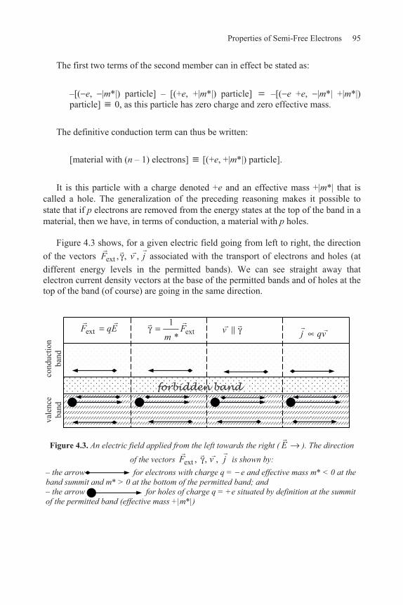
Properties of Semi-Free Electrons 95
The first two terms of the second member can in effect be stated as:
–[( e, |m*|) particle] – [(+e, +|m*|) particle] –[( e +e, |m*| +|m*|) particle] 0, as this particle has zero charge and zero effective mass.
The definitive conduction term can thus be written:
[material with (n – 1) electrons] [(+e, +|m*|) particle].
It is this particle with a charge denoted +e and an effective mass +|m*| that is called a hole. The generalization of the preceding reasoning makes it possible to state that if p electrons are removed from the energy states at the top of the band in a material, then we have, in terms of conduction, a material with p holes.
Figure 4.3 shows, for a given electric field going from left to right, the direction
of the vectors ext , , , F v j associated with the transport of electrons and holes (at different energy levels in the permitted bands). We can see straight away that electron current density vectors at the base of the permitted bands and of holes at the top of the band (of course) are going in the same direction.
extF qE ext1
*F
m v j qv
forbidden band
vale
nce
band
co
nduc
tion
band
Figure 4.3. An electric field applied from the left towards the right ( E ). The direction
of the vectors ext ,F , ,v j is shown by: – the arrow for electrons with charge q = e and effective mass m* < 0 at the band summit and m* > 0 at the bottom of the permitted band; and – the arrow for holes of charge q = +e situated by definition at the summit of the permitted band (effective mass +|m*|)
forbidden band

96 Solid-State Physics for Electronics
4.3. Expression for energy states close to the band extremum as a function of the effective mass
4.3.1. Energy at a band limit via the Maclaurin development (in k = kn = an )
Around k = k0 the Maclaurin development for the energy (E) can be written as:
2 2
( ) ( ) 2( )
( ) .2n
n n
nk k n
k k
E k k EE E k k
k k [4.9]
As in k = k0 we have a horizontal tangent (as [4.8]
0)n
dEdk k k
while the
effective mass is defined by m*= ²2 2( )
*E k
m [4.7], we obtain using equation
[4.9] when k kn:
n( ) (k )²
( )².2m*k nE E k k [4.10]
Note that this is the expression that replaces the expression ² ²2
km
E obtained
for free electrons.
NOTE 1.– In the neighborhood of the zone center, where n = 0 and k0 0, we thus find:
0( ) (k )²
E ².2m*kE k [4.11]
NOTE 2.– Equation [4.10] for the energy of an electron can be given as a function of |m*|. In this case we can write that:
n( ) (k )²
E ( )²2 m*k nE k k [4.12]
where the + sign is for m* > 0, that is, an electron at the bottom of the band, while the sign is for m* < 0, meaning an electron high up the band.

Properties of Semi-Free Electrons 97
4.4. Distinguishing insulators, semiconductors, metals and semi-metals
4.4.1. Required functions
Insulators, semiconductors and metals are discerned by the way in which the energy levels are filled by their electrons, the latter being characterized with respect to their electronic state (orbital wave function and spin, or so called “spin-orbit” as in
).N For a rigorous treatment, we should determine the (available) energy state density function for semi-free electrons, denoted Z(E) and the occupation probability function, similarly, denoted F(E) for these energy states in the different bands. The function produced, n(E) = Z(E)F(E), thus represents the density function of occupied (full) electronic states for each energy level (E). Also, n(e)dE represents the number of electrons per unit volume for which the energy is between E and E + dE.
In an original and simplifying step, we can state that for n(E) possible filling
configurations, each results in a particular electronic behavior and these behaviors can be classed with respect to four types of material, i.e. insulators, semiconductors, metals and semi-metals.
4.4.2. Dealing with overlapping energy bands
Generally, in a representation of E = f (k), shown in the upper part of Figure 4.2, the last band to be totally occupied by electrons is called the valence band. Its highest energy level is denoted EV. The first empty or only partially occupied band is called the conduction band. Its lowest energy level is signified by EC. However, when looking at 2D or 3D materials, it is no longer possible to see E simply as a function of k kx as in Figure 4.2 (that is, traced for a 1D system). In effect, the propagation wave vector k for each electron can be specified for each direction of propagation which might be listed as 1, 2, 3 and so on. This means that for the directions x, y and z of a material with optical/electronic axes Ox, Oy and Oz, there are different k values, i.e. k1, k2, k3, etc. The upshot is that different representations of E f (k) must be made for each direction. For example, say that direction (1) corresponds to the direction x used exclusively until this point. Along with this we have another direction (i) that has no specific alignment. In Figure 4.4 we can see how the representation of E f (k) can give rise to two different positions for the band limit energy levels denoted EVi and ECi for direction (1) with respect to the energy levels EV1 and EC1 for direction (1). Specifically, in case (Figure 4.4b) we have EV1 < EVi < EC1. Thus there is a resultant forbidden band in the crystal, of a size given by 1 .C Vi GE E E E In case (as in Figure 4.4b), we have EVi > EC1 and the forbidden band disappears because the energy levels of the conduction band of direction (1) start filling prior to the valence band of direction (i) being totally filled.

98 Solid-State Physics for Electronics
Figure 4.4. Plots of E = f(ki) for: (a) values of EV1 and EC1 fixed by a given direction k1; (b) the resulting cases and with different positions of EVi and ECi
Generally, when the forbidden band appears, it has a size given by the minimum value of E obtained from the difference between the minimum value of all the energies at the bottom of the conduction band (ECj) (for all directions j = 1, I, etc. under consideration) and the maximum value reached by the highest energy of the valence band (EVj) (again for all directions j = 1, I, etc.).
4.4.3. Permitted band populations
4.4.3.1. State density function Z(E)
As we saw for free electrons in Chapter 2, the state density function can be defined either in wavenumber (k) space (reciprocal space) or in the energy space given by E. For the latter and in 3D space, the relevant expression is given by (see also equation [2.31] in Chapter 2):
3/ 23
4( ) (2 ) .Z E m E
h [4.13]
For these free electrons, where there is no interaction potential with the lattice, the function Z(E) is thus parabolic.
k1
E
1a
EC1
EV1
ki
E
ia
ECi
EVi
ki
E
ia
ECi
EVi
Case ( ) Case ( ) Figure (a) Figure (b)
EG

Properties of Semi-Free Electrons 99
For semi-free electrons or holes, the interaction of carriers with the lattice means replacing the mass (m) of free electrons with the effective mass of the carrier under consideration. Semi-free electrons, which have an effective mass denoted by me*, are distributed in the conduction band from the bottom up, the bottom being level EC rather than zero energy, as would be the case for free electrons. The state density function can be calculated just as for free electrons, with the exceptions that m and (E – 0) E are respectively replaced by me* and (E – EC). Equation [4.13] now takes on a form shown below as equation [4.14]. This equation also shows a parabolic evolution for energies such that E > EC (see Figure 4.5).
* 3/ 23
4( ) (2 ) ( ).C e CZ E m E E
h [4.14]
Similarly, semi-free electrons are distributed in the valence band from the summit of the band, i.e. EV downwards so that the state density function is parabolic towards energies, such that E < EV. With function Z(E) still being positive, it is the absolute value of the effective mass that must be brought into play, so that we now obtain:
* 3/ 23
4( ) (2 ) ( ).V e VZ E m E E
h [4.15]
To take these differences into account, if we denote the band limit by En (so that En is equal to either EC or EV), and make m* the general term for the effective mass of the carrier (be it electron or hole), then the general expression for the state density function for all types of carriers is:
* 3 / 23
4( ) (2| |) .nZ E m E E
h [4.16]
We can now represent the overall evolution of the state density function Z(E) for electrons in Figure 4.5, where just as in section 4.4.2 we can distinguish two specific situations:
– case where there is no band overlapping and there is an energy gap such that E EG;
– case where there is an overlap of valence and conduction bands and as a consequence a suppression of the forbidden energy zone.

100 Solid-State Physics for Electronics
Figure 4.5. State density function for semi-free carriers
where there: ( ) is no band overlap; and ( ) is band overlap
4.4.3.2. Occupation probability function F(E)
Fermi-Dirac distribution is necessary when describing the distribution of electrons (or holes), as it governs the quantum behavior of a range of specific particles:
– under thermodynamic equilibrium;
– without mutual interactions; and
– likely subjection to an external field. This is in effect a Boltzmann distribution modified by a condition due to the
Pauli principle. Using Fermi statistics (details of which can be found in most courses on thermodynamic statistics) the occupation probability of a given energy level E by electrons is described by the Fermi-Dirac function (where EF is Fermi energy):
1( ) .
1 exp E EFkT
nF E [4.17]
This function is such that Fn(EF) =1/2. When T 0K we have Fn (E < EF) = 1 and Fn (E > EF) = 0 (see Figure 4.6b). When T 0K, we obtain the result plotted in a continuous line in Figure 4.7b.
Z(E)
EO EV EC
( )
ZC(E)ZV(E)
Z(E)
E O EV EC
( )
ZC(E) ZV(E)Z(E)
EG

Properties of Semi-Free Electrons 101
To obtain the distribution law for holes denoted Fp(E), we first note that a given energy level E is either occupied by an electron or occupied by a hole (electron vacancy). This trivial condition is transcribed as Fn(E) + Fp(E) = 100% = 1, so that we can state that:
Fp(E) 1 – Fn(E) 1 1
1 exp .FE EkT
[4.18]
This function is such that Fp(EF) 1/2, and when T 0K we have Fp (E < EF) 0 and Fn (E > EF) = 1 (see Figure 4.6b). When T 0K, we find the representation given as a broken line in Figure 4.7b.
Z(E)
EEpot EV EC
Case ( )
ZC(E)ZV(E)
Z(E)
E Epot EC EV
Case ( )
ZC(E) ZV(E)
Z(E)
Fn(E)
n(E)
Fp(E)
p(E)
E
E
EF(0)
EV EC
1
1/2
Fn(E)
n(E)
Fp(E)
p(E)
E
E
EF(0)
1
1/2
valence band filled with electrons
occupied levels (CB)
(a)
(b)
(c)
(a’)
(b’)
(c’)
Figure 4.6. At absolute zero, a qualitative evaluation of the function n(E) from functions Z(E) and F(E) when EF is localized mainly in the middle of the forbidden band in a system of:
( ) non-overlapping bands; and ( ) overlapping bands
conduction band empty of electrons
empty band levels
EG
Epot

102 Solid-State Physics for Electronics
Figure 4.7. For T 0K, qualitative evaluations of the function n(E) from functions Z(E)
and F(E) when EF is well localized in the middle of the forbidden band for a system of bands that: ( ) do not overlap; ( ) overlap
4.4.3.3. Electronic densities in the permitted bands: distinction between insulators, semi-conductors, metals and semi-metals
If n(E)dE represents the number of electrons per unit volume having energy between E and E + dE, the electronic density n(E) is equal to the product of the number of available states between E and E + dE (or rather Z(E)dE) and the occupation probability Fn(E) of these states. This can be stated as n(E) Z(E)Fn(E).
Similarly, for holes we will have a density p(E) given by p(E) Z(E)Fp(E). The equations for these densities will be developed in the second volume entitled Electronics and Optoelectronics of Materials and Devices. For now, we will limit ourselves to qualitatively studying the filling of permitted bands.
Z(E)
EEpot EV EC
( )
ZC(E)ZV(E)
Fn(E)
n(E)
Fp(E)
p(E)
E
E
EF
EV EC
Occupied VB levels
Occupied CB levels
Empty valence band levels
Empty conduction band levels
(a)
(b)
Z(E)
E Epot EC EV
( )
ZC(E) ZV(E)
Z(E)
Fn(E)
n(E)
Fp(E)
p(E)
E
E
EF
1
1/2
Occupied CB levels
(a’)
(b’)
(c’)
Empty levels
1/2
1
(c)

Properties of Semi-Free Electrons 103
4.4.3.3.1. When at absolute zero
In Figure 4.6 the Fermi level is placed broadly in the middle of the gap – a position that will be justified later on for semiconductors – however, it can be found in the permitted band as in the case of certain metals.
Qualitatively, at absolute zero, when there is no band overlap, as in case on the
left, the last occupied band is totally filled (valence band) while the following band is totally empty (conduction band) as in Figure 4.6c. The electronic gap EG (width of the forbidden band) is thus determined by the difference in energy between the base of the conduction band (EC) and highest point of the valence band (EV). When this gap EG EC – EV is:
sufficiently large (typically > 5 eV) to stop significant passing of electrons between bands by thermal agitation kT (Figure 4.7), the material is considered to be an insulator;
sufficiently narrow (typically < 3 eV) to allow significant passing of electrons from the valence to the conduction band by thermal agitation kT (Figure 4.7), the material is considered an intrinsic semiconductor.
Qualitatively, at absolute zero, when there is a band overlap, as in case on the
right-hand side of the figure, all the levels below EF are filled while those above remain empty. This partially filled band is in reality a conduction band. The position of the Fermi level at absolute zero EF(0) is thus defined by the equality:
pot
(0)( )
FE
EZ E dE density of electrons in the conduction band
where Epot is the potential energy at the base of the conduction band. In fact two situations can be distinguished in this latter situation:
– either the overlap of the bands is weak and few states are involved so as to give a semi-metal; or
– the overlap of bands is strong with many states involved and we have a metal. Outside the case presented in Figure 4.6 where the Fermi level is in the center of
the forbidden band, we should also consider the case where EF is found within a permitted band. In this situation, the states of the permitted band are filled up to the level EF and then bands above EF are empty. With the occupied states not separated from the empty states by a forbidden band, we have a metal.
104 Solid-State Physics for Electronics
4.4.3.3.2. When T 0K
Here the function Z(E) is not modified, while the Fermi function does not suddenly pass from a value equal to one to being equal to zero (and vice versa) in E EF. The change occurs progressively, more so as T increases.
In case on the left-hand side of Figure 4.7, there is no overlapping of the bands. We can now see that there are states at the top of the valence band (VB) that are unoccupied (partially filled band) while there are some states at the bottom of the conduction band (CB) that are becoming filled. The movement of electrons from the valence to the conduction band is even greater when EG is small (as in semiconductors) and when the temperature is high. With the total number of electrons remaining constant in a given volume, the number of empty levels in the VB must be equal to the number of filled levels in the CB. Because function Z(E) varies as a parabola in both the heights of the VB as well as in the depths of the CB and function F(E) is symmetric around the Fermi level (at point EF, ½), the Fermi level must be placed well near the middle of the forbidden band so that the empty and hatched surfaces shown in Figure 4.7c of the VB and the CB, respectively, are equal, so that:
1.
2F V CE E E
In case on the right-hand side of Figure 4.7, where there are overlapping bands, the abrupt transition at T 0K between the full and empty level is considerably smoothed at T 0K. The permitted band levels remain partially empty and the metallic or semi-metallic behavior is retained when T 0K, regardless of temperature.
4.4.3.3.3. Conclusion
A normal representation of the band scheme is given in Figure 4.8, where we are now dealing with an intrinsic semiconductor. The electronic and hole state density functions, n(E) and p(E) respectively, are detailed.
Other band representation schemes are used, in particular that of reduced zones (see also section 3.6.2). Instead of representing the dispersion curve E f (k) over all variations in k (which would bring in various values of k as in , 2 ,3 ,
a a ak etc.,
for which we would see the discontinuities shown in Figure 4.2 for insulators and semiconductors), the E = f (k) is represented simply for values of k between
a and
.a
However, this is also for the whole energy range brought into the zone given

Properties of Semi-Free Electrons 105
by , .a a
The curves represent energy with the help of an appropriate
translational modulation of the form 2 a
n (translation modulation equal to that of
an appropriate vector of the reciprocal lattice so that the translation conserves its Bloch function properties in each zone. This is further described in Figure 4.9 where the number of each zone is also shown.
Figure 4.8. (a) Band filling for a intrinsic semiconductor; (b) state density
functions; (c) occupation probability functions; and (d) concentration functions
The representation shown in Figure 4.9 is that of a 1D medium (see section 3.6.2) when the extremities of the curves are at k 0. In a 2D or 3D media, where the overlapping zone is not necessarily in the same direction, we can end up with the schemes shown in Figure 4.10. In the direction kx where the lattice repeat unit is denoted by a, the various zones are brought back into the zone defined by the
interval 0, .a
Similarly, in the ky direction where the lattice repeat unit is
denoted by b, the various zones are brought back into interval 0, .b
Figure 4.10a
thus represents an insulator/semiconductor (lower band full and upper band empty at T OK), Figure 4.10b for a metal with the last occupied band being partially full (leaving free the upper part of the band where electrons can move when influenced for example by an electric field), and Figure 4.10c for a semi-metal due to the weak overlap of bands.
EF
EC
EV
Z(E)
E
O
EC EV
F(E)
E
O
EC EV
Fn
Fp
Carrier concentration
E
O
EC EV
n(E)
p(E)
(a) (c)(b)(d)
Hole
Electron
BC
BV

106 Solid-State Physics for Electronics
Figure 4.9. Diagram of reduced zones, where each zone is given an n number
k
a
a
E
O
n 1
n 3
n 2
Figure 4.10. Band structure for: (a) an insulator with a fully occupied last band; (b) a metal where the last occupied band is only partially filled;
and (c) a semi-metal with band overlap
kx
a
E
O
(a)
ky b
EG
ky kx
a
E
O
(d)
b
(b)
kx
a
E
O ky b

Properties of Semi-Free Electrons 107
4.5. Semi-free electrons in the particular case of super lattices
A practical example can be given using the problem below.
A heterostructure is based on three pieces of semiconductor (SC) as shown in the figure just below. A thin SC1 slice of thickness denoted d along Tz and in the order of 10 nm is sandwiched between two layers of the same SC2. In directions Tx and Ty the L dimensions of SC1 and SC2 are considerably greater than d. Finally, the “gaps” of SC1 and SC2, respectively denoted as EG1 and EG2, are such that EG1 < EG2.
Figure 4.11. Heterostructure based on three pieces of semiconductor
The heterostructure can be represented by a theoretical model in which movement is separated into a particular plane of the structure (plane cTy) and in the perpendicular direction (Tz). The function is thus given as:
(x, y, z) (z) (x, y),
and it is assumed that the electronic states at the SC1 level of the SC are those of an electronic gas (at zero potential) in 3D, with an effective mass m* (which thus takes interactions between electrons and the lattice into account as m* m where m is the mass of a free electron).
It is also assumed that these electrons:
– move freely in planes parallel to xTy; and
– exhibit limited displacements within zone 0 z d due to the existence of potential barriers (that are assumed to be infinite within z 0 and z d in this theoretical study).
L
y
x
L
L
0 d
L (L >> d)
T z
SC1
SC2 SC2
O D

108 Solid-State Physics for Electronics
Before approaching the example problems, we should note that if the wave function is the product of two functions, as in (x, y, z) (z) (x, y), then the energy solution from the Schrödinger equation is given by E Ez + Ex,y and the behavior in this system is the same as that in a classical potential box.
1)
a) Write the Schrödinger equation for the displacement of electrons (in SC1) in the perpendicular direction (Tz).
b) Give the form of the wave function [ (z)] using fixed boundary conditions (FBC) that gives a stationary solution and for which the wave function takes nodes as extremities. Justify this choice.
c) Deduce the conditions for quantification (with the help of a quantum number denoted nz for which the values will be given) of the wave vector (component kz) and corresponding energy Ez.
d) With m* (AsGa) = 0.066 m (where m is the ususal mass of the electron) and d = 10 nm, give the numerical value of the first three permitted energies
1 2 3, , z z zE E E in eV.
2)
a) Write the Schrödinger equation for the displacement of electrons (in SC1) in the plane xTy.
b) Give the form of the wave function (x, y). Justify the use of progressive boundary conditions (PBC, otherwise called Born Von Karman boundary conditions) to determine the quantification conditions (with the numbers nx and ny to be determined) of the wave vector (components kx and ky). As indicated in the figure, extensions of the semiconductor in directions Tx and Ty are equal to L, where L is considerably greater than d by several orders of size.
c) Deduce the energy values , .x yE
3) Give the final expression for the quantified energy of the electrons of SC1 and determine the minimum value (E1) of this energy.
4) Making k// 2 2x yk k and k = kz:
a) give on the same plot the dispersion curve for Ex,y f (k//) and Ez f (k ), and then E f (k//) and E f (k );
b) detail the progressive filling of the permitted level. Determine, in particular, the conditions on nx and ny when going from nz 1 to nz 2;

Properties of Semi-Free Electrons 109
5) For direction Tz, we suppose that the touching semiconductors have the same reference potential (vacuum level) and it is with respect to this that we place the bottom of the conduction bands (due to electronic affinities 1 for SC1 and 2 for SC2). The structure used in this example is: AlAs/GaAs/AlAs where in eV we have:
EG1 (GaAs) = 1.43, EG2 (AlAs) = 2.16,
1 (GaAs) = 4.07,
2 (AlAs) = 3.5.
a) Describe the positions of the conduction band minimums and valence band maximums for structure SC2/SC1/SC2 with respect to Tz. It should be noted that, if required, the electronic affinity is the difference in energy between the vacuum level and base of the conduction band.
b) Indicate the height of the potential barrier at the interface SC2/SC1. Give an approximate position of the above evaluated energy levels
1,zE
2,zE
3zE on the
diagram. Detail the nature of approximations made on this result in order to give the approximate energy levels.
c) Also give the position Ez1(t) of the holes in GaAs by taking for their effective mass the value |m*(t)| = 0.68 m.
d) From this deduce the radiation energy that might be emitted from GaAs.
Answers
In order to study the electronic states in a superlattice structure, where there are two semiconductors that are such that EG1 < EG2, we can denote two types of movement:
– one along Oz where SC1 presents a small dimension d, for which we will privilege the stationary solutions for the wave function through the use of FBC; and
– one along directions Ox and Oy where SC1 has a large dimension with respect to d (plan0065 xTy). Progressive solutions are favored for the wave function through the use of PBC.
We make ( , , ) ( ) ( , )x y z z x y (separation of variable), and the energy will be in the form , .z x yE E E
1)
a) With respect to Tz, the Schrödinger equation is written as: *² 2
² ²0m
z zE .

110 Solid-State Physics for Electronics
b) By making 2 *²
² ,mz zk E the stationary solutions for the wave function
can be written as: ( ) .ikz ikzz Ae Be
The use of FBC for the direction Oz where SC1 has a small dimension makes it possible to state that the wave function presents a node at the origin: (0) 0, from which 0, or rather A B A B and from which it can be deduced that
2( ) 2 ,
ikz ikze ez A which can also be written in the form:
2( ) 2 2 sin .
ikz ikze ezz A iA k z
Assuming that the wave function has a node at each extremity is the same as assuming that at these extremities the barrier between adjacent semiconductors is practically infinite, which will require verification a posteriori.
c) The alternate limiting conditions thus give (d) = 0, which results in sin kzd 0, from which ,, so that also
dz z z zk d n k n where nz 1 and
an integer and not equal to zero. The latter is because otherwise the solution would give (z) = 0 which would correspond to the absence of particles with a presence probability equal to zero.
We can go on to deduce that ² ² ² ² ²2 * 2 * ² 8 * ²
² ².k hzm m d m dz z zE n n
d) We find:
1
2
3
0.057 eV,0.23 eV,0.52 eV.
z
z
z
EEE
2)
a) Schrödinger’s equation for the plane xTy is written as:
*
,² ( , ) ² ( , ) 2
( , ) 0² ² ² x y
x y x y mE x y
x y
b) The separation of variable is obtained by making:
( , ) ( ) ( ),x y X x Y y
Properties of Semi-Free Electrons 111
from which we find energy in the form , .x y x yE E E Placing this in to the Schrödinger equation we obtain the sum for the two equations independently in x and y directions:
² ( ) 2 *( ) 0
² ²² ( ) 2 *
( ) 0.² ²
x
y
X x mE X x
xY x m
E Y yy
By making 2 *2
2 mx xk E and 2 *
22 ,m
y yk E the search for progressive
solutions with respect to these large dimensions x and y leads us to (with respect to x):
( ) .xik xX x Ce
The use of the corresponding PBC for progressive solutions makes it possible to
write that: ( )( ) ( ) ,x xCLP
ik x ik x LCe X x X x L Ce from which is deduced that
1.xik Le
The upshot of this is that we should have 2x xk L n with .xn nx is an integer that can be positive, negative or zero. The last value will simply yield a constant probability presence.
Similarly, for Oy we obtain: 2 with *.y y yk L n n
c) From the preceding values of kx and ky we can deduce the value of the energy for movement in the plane xTy:
2 2,
2
²2 *
² 2 ² ²
2 *²
² ²2 * ²
x y x y x y
x y
x y
E E E k km
n nm L
hn n
m L

112 Solid-State Physics for Electronics
3) The final expression for the quantified energy E of electrons in SC1 can thus be written as:
,
22 2
22 2
² ² 4
2 * ² ²
² 4 .
8 * ² ²
z x y
zx y
zx y
E E E
nn n
m d L
h nn n
m d L
The minimum value in E, denoted E1, for the lowest values in nz, nx and ny, i.e. 1zn and 0x yn n gives:
110
².
8 * ²z
x y
nn n
hE E
m d
4)
a) By making 2 2/ / x yk k k and ,zk k we can trace the dispersion
curves for Ez f (k ) and Ex,y f (k//), from which we can deduce the curves E Ez + Ex,y f (k//) and E f (k ). See the following figure obtained by observing the comments below.
In particular, we can note that:
– on the other hand:2 2 2 2
22 * 2 * 2 *2 2 2 ,
m m m dz z zE k k n where nZ 1, 2,
3,… and d
is large as d is small (with respect to L), so that zE is large (compared
to , ),x yE and that 1 1( ) ;zz nE E
– on the other hand: 2 2 2 2
2 * 2 * 2 *
22 2 2 2 2, ( ) = ( )
m m m Lx y x y x yE k k k n n
where xn and yn and 2L
is small, as L is large (with respect to d).
The result is that ,x yE is small (with respect to ),zE and that k can be
written as 2 2 2 40, , 2, 2 ,...L L L L
k

Properties of Semi-Free Electrons 113
b) The progressive occupation of levels is in the order E1, E 2, E 3, E 4 and so on, as shown in Figure 4.11. As long as 2 1 , ,[ ] ,
x yz z x y n nE E E the obtained
energy E remains that obtained with nz 1, so that:
22 2 2 2² ² ² ² ² 2
2 1 ,2 * ² 2 * ² 2 * x yn n
m d m d m L
from which we can deduce:
2 2² 4 ²3 ,
² ² x yn nd L
thus giving the condition: 3 ²4 ²
2 2 .Ldx yn n
d
2d
2L
22
L
4L
k
k
E
O
Ez1 = E1
Ez2
0,0
x
y
nx yn
E
1,0
x
y
nx yn
E
1,1
x
y
nx yn
E
2,0
x
y
nx yn
E
12 1 ,0
x
y
nz x yn
E E E
13 1 ,1
x
y
nz x yn
E E E
E4
Figure 4.12. Dispersion curves of Ez = f(k ) and Ex,y = f (k//) from which we can obtain the curves of E = Ez + Ex,y = f (k//) and E = f(k )

114 Solid-State Physics for Electronics
Thus, to go from nz 1 to nz 2, it is necessary that 3 ²4 ²
2 2 .Ldx yn n
5)
a) Taking the potential energy origin to be the vacuum level, the energies in the direction Tz are spread as indicated in Figure 4.12.
In direction Oz, the energy levels are quantified and the discrete levels
correspond to those of a potential well, as shown in the figure above for levels Ez1, Ez2, and Ez3. Due to the energy difference between conduction bands, the electrons in the conduction band of SC2 accumulate in the potential wells formed in the conduction band of SC1. If SC2 is doped, this number of electrons is high while SC1 is highly degenerate without even being doped. In other words, there is a high number of electrons in the conduction band so that the semiconductor degenerates towards a metallic state. The spatial separation of a high number of electrons into SC1 as diffusion centers (as many as there are doping agents in SC2) favors a high mobility of electrons in SC1.
Figure 4.13. Energy levels in the structure AlAs/Ga As/AlAs
b) The potential height of the interface between SC2 and SC1 is:
W0 = 1(GaAs) – 2(AlAs) = 0.57 eV.
SC2 SC1 SC2
vacuum level
2
1 = 4
.07
eV
E G1=
1.
43 e
V
O d
2 = 3.5 eV
E G2=
2.16
eV
1 - 2 = 0.57 eV
h = 1.6 eV
0.16 eV
E z1(t
) =
5.
7 m
eV
z
Ez1
Ez2
Ez3EC
EV

Properties of Semi-Free Electrons 115
In the potential wells, along Oz we can place the Ez levels (relative to the base of the conduction band):
1
2
3
0.057 eV,0.23 eV,0.52 eV.
z
z
z
EEE
Finally, the approximation of an infinite height for the potential wells previously used to determine wave functions and energies is acceptable when electrons are situated on the level denoted Ez1; however, it is no longer acceptable for level Ez3.
For holes, the barrier is given by:
2 2 1 1 5.66 5.50 0.16 eV.G GE E
c) With respect to the summit of the GaAs valence band (with EV = 0), the position of the hole accepting layer is given by:
02 2 2 2 21
2 21 * * 2 2*( ) 5.7 meV.
2 2 2
V
z
En
z V z V zt t t
E t E k E nm m d dm
d) The transition has a frequency such that:
1 1 1( ) 1.6 eV.z G zh E E E t
We should note that Ez1, like Ez1(t), can be adjusted by a change in the value of d (width of the GaAs slice). This makes it possible to change the frequency (and thus the wavelength) of the emission.
We can also note that the frequency that is emitted is as high as that emitted by GaAs alone. In addition, as the extrema of the CB and VB bands are localized on the same SC1 (GaAs), recombinations are direct and very easy, and this it what defines a so-called type I heterostructure. They find applications in devices such as lasers, due to their high efficiency in photon emission. They were first described by L. Esaki, a winner of the Nobel Prize for physics in 1973.
The deposition of such structures in multi-layer structures, with a periodic repetition along Tz, introduces a supplementary periodicity that spreads the Ez levels into bands of electrons or holes.

116 Solid-State Physics for Electronics
4.6. Problems
4.6.1. Problem 1: horizontal tangent at the zone limit (k /a) of the dispersion curve
Using the relation E f (k) obtained in Chapter 3 for a
k (equation [3.16]),
show by calculation how the energy curves E f (k) give a horizontal tangent at the points where the energy becomes discontinuous.
Answers
The theory for semi-free electrons in a 1D medium (section 3.2.4) makes it possible to state that for values of k close to
a (coefficient A1 being large) there is
a double condition on the value of the energy that equation [3.16] translates as:
22 0
42 2 ²
²² ²μE μE μ w
k k
where 2 .a
The left-hand side member is a function of E and k, while g (E, k) is such that
2² 04( , ) .
μ wg E k If we differentiate this equation, we obtain ' ' 0,E kg dE g dk
or rather '
' .dE gkdk gE
As we wish to show that 0,dEdk k
a
it suffices from the
preceding equation to show that '[ ] 0.k
akg So, calculating '
kg gives us:
2' 2 2 2 2
2 ² 2 ,² ²k
g μE μEg k k k k
k a a
from which
' 2 2 ² 2 ²2 0,
² ² ² ²k ka
μE μEg
a a a a
which is the answer required.

Properties of Semi-Free Electrons 117
4.6.2. Problem 2: scale of m* in the neighborhood of energy discontinuities
1) The preceding sections detailed two conditions on energy for semi-free electrons placed in a potential defined by V(x) w0 cos x. Now show that:
20 0 0 0 20
1.
2 k k k kE E E E E w
2) In the neighborhood of a discontinuity, we can state that a
k k where
ak and k > 0 or k < 0. By making ²
2
20 ,m aBE show that:
00 0
0
² 4² 1 .
2 2B
BE w
E E km w
3) Give the limiting values for E for a discontinuity obtained for a
k . From
this deduce the size of the forbidden band.
4) In this problem, |w0| 2 eV and a 0.3 nm. Calculate the ratio *mm
for the
bottom of the second band and for the top of the first band.
Answers
1) The theory for semi-free electrons in a 1D medium makes it possible to state that for values of k close to
a there is a double condition on the energy value. The
compatibility of these two conditions brings us to equation [3.16]:
2 20²² ²
.2 2 4
kk wE E
μ μ

118 Solid-State Physics for Electronics
By making ² ²2
0 kμkE and
2²2
0 k
μkE (where 2 ),a
this equation
can also be written as 20
40 0( )( ) ,
wk kE E E E which is a second degree
equation:
0 02
0 0 0² ( ) 0.4k k
wE E E E E Ek k
Its solution is written as:
220 0 0 0 0 0 014 ,
2 4k k k k k kw
E E E E E E E
which is also written as:
20 0 0 0 20
1.
2 k k k kE E E E E w
2) The preceding equation is for energy in the neighborhood of 2
.a
k
Making
2,
ak k k where k > 0 at the top of the band, and k < 0
at the bottom of the band, and in addition assuming that ,a
k we have for
values of 2
k k the equations ² ²2 4
0 ²μkE k k and
² ²2 4
0 ² .μkE k k
Under these conditions the preceding equation for E can be written as:
1/ 22
0 20
1 ² ² ² 4 ² ²2 ² 1 .
2 2 2 2k
E k wm m w

Properties of Semi-Free Electrons 119
By making
22 2
0 0² ²,
2 2 2
aB k aE E
m m a
the two solutions for energy are such that: – first solution:
12 2 2 2 2 20 2 0
(1) 20
12 2 2 22 00
20
2 02 0
0
4.41
2 2 2 2 4
4.4 1
2 2 2
4 1
2 2
B
B
B
w kE E k
m m m w
w kk E
m m w
E wk
m w
– second solution:
00 0
(2)0
² 4² 1 .
2 2B
BE w
E E km w
Both solutions can be brought together in the equation written:
00 0
0
² 4² 1 .
2 2B
BE w
E E km w
3) At the limit, as 0:k – the second solution goes towards
0 0(2) .
2Bw
E E

120 Solid-State Physics for Electronics
With w0 < 0, this solution is for the bottom of the band where the value of k introduced into the initial expression, ,
ak k must be negative.
– the first solution tends towards 0 .2
0(1)
wBE E
With w0 < 0, this solution is for the top of the band where the value of k must
be positive.
The gap between the two solutions for the energy is equal to |w0| = EG.
4) To calculate the effective mass at the top of the band (where it must be negative), we will use the expression for E corresponding to the first answer to problem 2, that is:
00 0
(1)0
² 4² 1 .
2 2B
BE w
E E km w
This gives the effective mass as ²1 1 (1)
* ² ²(1).
E
km Because
2,k k we can
note that
(1) (1) (1) (1) (1)² ².
² ²
E E E E Ekk k k k k k
k
E
EB0 w0
first solution
second solution

Properties of Semi-Free Electrons 121
With
0(1)
0
² 41 ,BE E
kk m w
from which
0(1)
0
² ² 41 ,
²BE E
k m w
we deduce that:
0(1)
*0(1)
²1 1 1 41 .
² ²BE E
k m wm
Numerically, with w0 = –2 eV and a 0.3 nm, we obtain 0 4.2 eV,BE from which:
*(1) 0.135.
m
m
To calculate the effective mass at the bottom of the second band (where it must be positive) we use the second expression for E found in the answer to problem 2, i.e.:
00 0
(2)0
² 4² 1 .
2 2B
BE w
E E km w
This gives the effective mass as:
0(2) (2)
*0(2)
² ²1 1 1 1 41 ,
² ² ² ²BE E E
k k m wmso that *
(2) 0.106.m m

122 Solid-State Physics for Electronics
In the figure above, we can note that if w0 is large (strong interaction with the
lattice) the permitted bands are relatively narrow (flat) and ² ²d E dk is small. Close to the discontinuity, 1* ² ²m d E dk is thus just as large (or small) as the interaction is strong (or weak). When k increases (on the right of the discontinuity)
² ²d E dk decreases and m* increase up to a infinite value in the middle of the permitted band (m* is at a minimum at the base of the band).
4.6.3. Problem 3: study of EF(T)
We showed in Chapter 2, problem 4 that Fermi level of a 3D metal was practically independent of temperature, assuming the conduction electrons are free electrons. Is this property still valid if the electrons of the metal are assumed to be semi-free?
Answers
For a 3D metal that has a metallic character originating from electrons placed in an incompletely full conduction band (typically half-full as indicated in Chapter 6), the state density function [Z(E)] takes on the same form for semi-free electrons as for free electrons. Only the nE E term must be replaced by the term ,E where En EC is the potential energy of the bottom of the conduction band. The other functions (Fermi-Dirac notably) remain invariable. Simplifying, so as to not have to go through the calculations again, we can suppose that a judicious choice of origins at the bottom of the conduction band will suffice (so that En EC 0), as this choice is the same as fixing the value of nE E to that of .E Z(E) thus takes on exactly the same form as for the free electrons as long as the mass of the electron is replaced by the effective mass of the semi-free electron. The property of quasi-invariability of the Fermi level with temperature is thus retained when going from using free to semi-free electrons to represent metal electrons.
k
E
EB0 w0
large w0 small
² ² larged E dk
² ² smalld E dk

Chapter 5
Crystalline Structure, Reciprocal Lattices and Brillouin Zones
5.1. Periodic lattices
5.1.1. Definitions: direct lattice
A lattice is a periodic (hence regular) arrangement of points called nodes. At each node the base of an atom is attached, the nature of which depends on the solid.
In 3D, the lattice is defined by three fundamental vectors denoted , ,a b c that are such that the atomic arrangement is identical around a point P defined with respect to the origin O by ,r OP and around a point P’ defined by ' '.r OP The vector
'r must be such that 'r r T where T is a translational vector defined by
1 2 3 ,T n a n b n c and where n1, n2 and n3 are integers.
Furthermore, we can see that the lattice, which is characteristic of crystalline structures, is created by the addition (superposition) of the base (ellipsoid) to each node (point) of the crystal.
Thus, any two points of a lattice are always linked to one another by an appropriate translational vector .T

124 Solid-State Physics for Electronics
Figure 5.1. Imaginary crystal element where nodes are represented by points encircled by an ellipsoid, representing the base of an atom
In the 2D figure above we can see that the atomic environment is identical around points P and P’ with each being linked to one another by the vector
1 2T = n a + n b which is such that n1 = 2 and n2 = 3. The vectors a and b shown in the figure are fundamental vectors.
The parallelepiped defined by the fundamental vectors , ,a b c is called the primitive unit cell, and is the smallest unit possible. The volume of the primitive unit cell is equal to | ( ) |.cV a b c On average, each parallelepiped unit cell contains one node, and each node is shared with four cells below and four cells above the base plane of the node itself. In effect, each node is shared between eight cells and as there are eight nodes per cell (at the eight tops of the parallelepiped) with each being shared with eight other cells, we have an average of one node per cell.
Figure 5.2. Parallepipedic structure with an average one node per cell
The various crystalline structures belong to different types of lattice. In all there are fourteen Bravais lattices (or “space lattices”), with the simplest structures being simple cubic (sc), body-centered cubic (cc), face-centered cubic (fcc), tetragonal, orthorhombic, hexagonal, triclinic, etc. (see any good book on crystalline structures for futher details).

Reciprocal Lattices and Brillouin Zones 125
5.1.2. Wigner-Seitz cell
There is another type of primary cell with a volume equal to = | ( ) | .cV a b c It is the Wigner-Seitz cell that is found in the following manner. As shown in Figure 5.3:
– the lines between a given node and its neighbors are traced;
– another line (or plane in the case of 2D lattices) is drawn normal to the first lines at their mid-points; and
– the volume (or the smallest surface) enclosed by these lines (or plane) is the Wigner-Seitz primary cell. This cell can cover or fill the whole space of the lattice.
Figure 5.3. Wigner-Seitz cell
5.2. Locating reciprocal planes
5.2.1. Reciprocal planes: definitions and properties
All nodes of a lattice can be grouped into classes of parallel and equidistant planes called reticular planes (there are in reality an infinite number of reticular planes). The position and orientation of a reticular plane is determined by any three points (nodes) in this plane. If the base contains only one atom, then the plane contains three unaligned atoms. These nodes can, in certain cases, determine the so-called cleavage plane.
5.2.2. Reciprocal planes: location using Miller indices
5.2.2.1. Definition of indices
If each of the three nodes that define the reciprocal plane are on an axis that carries the fundamental vectors , , ,a b c then the reciprocal plane can be determined

126 Solid-State Physics for Electronics
using the abscissae of the nodes with respect to the axis. So if, for example, the three nodes defining the reciprocal plane have the coordinates (with respect to the origin of the fundamental vector) (m, 0, 0), (0, n, 0) and (0, 0, p), then the plane can be found using the respective numbers indicated by m, n, and p. An example is shown in Figure 5.5a using the nodes M, N and P.
If a reciprocal plane is parallel to one of the fundamental vectors, then the preceding numbers are infinite (see Figures 5.5b and 5.5d). To remove this slight inconvenience, we can use Haüy indices, which are the inverse of the preceding numbers. The result is given in simple fractions (that Haüy termed rational indices) that are rather difficult to manipulate. Because of this, Miller proposed the use of whole indices obtained from the multiplication of simple fractions 1 1 1, ,
m n p by the
same number K. K should be as small as possible so that the result is a succession of integers (hkl). These numbers are called Miller indices, and are such that:
1 1 1, , .h K k K l K
m n p
For example, the coordinates of the point of intersection between a reciprocal plane and the axis of the fundamental vectors , ,a b c are: (4, 0, 0), (0, 1, 0) and (0, 0, 2). With K 4, we have:
1 14 1 ; 1 4 4 ; 4 2 .
4 2h k l
The resulting Miller indices are written in brackets, i.e. (142). If a reciprocal plane cuts through the negative part of the axis, then the
corresponding index is negative. This is indicated by writing the negative sign above the index concerned, as in ( )hkl for an intersection between the reciprocal plane and the axis carrying c (see Figure 5.5c).
The directions in a crystal are also defined by the three integers h, k and l, but
this time using square brackets, as in [hkl]. They are also such that they are the smallest possible integers proportional to the directing cosines of the angles formed between the direction considered and the cell axis. The direction given by [hkl] is only perpendicular to the planes defined by Miller indices in very specific cases, such as when involving the cubic structure.

Reciprocal Lattices and Brillouin Zones 127
5.2.2.2. Equation for reciprocal planes located with Miller indices
Figure 5.4 shows a system of axes and a plane ( ). OH is the line that passes through the origin O and is normal to the plane ( ). u is the unit vector in the direction OX that carries OH. The vector has components (cosine directors) denoted
, , .
Figure 5.4. Location of the plane ( )
For a point (A) (with coordinates x, y, z) to belong to the plane ( ), it suffices that its projection on the axis OH is at H. Thus, ,u OA OH and by making
,OH e we obtain:
,x y z e
which can be rewritten as:
1.e
x ye e
If A M (m, 0, 0), where M is the point of intersection between ( ) and Ox, the preceding equation for the plane where y z 0 gives 1,
em so that 1 .
e m
Similarly, by making A tend towards N (0, n, 0) and P (0, 0, p) we can successively
( )
u
X
x y
z
H
A (x, y, z)
i j
k
O
e

128 Solid-State Physics for Electronics
deduce that 1e n
and 1 .e p
On substituting these values into the equation for
the plane ( ), we now obtain:
1.x y zm n p
The Miller indices of the plane ( ) are: 1 1 1, , ,m n p
h K k K l K and the
equation for the plane (hkl) is thus given by: .hx ky lz K
5.2.2.3. Examples using the simple cubic system
Figure 5.4 shows four examples of a simple cubic structure with its side length equal to a and with different reciprocal planes located by Miller indices.
5.3. Conditions for maximum diffusion by a crystal (Laue conditions)
5.3.1. Problem parameters
A crystal can be seen as made up of nodes that carry charges (being attached to atoms or ions) capable of re-emitting (more often called diffusing) an incident wave in any direction. Here we are concerned with discovering the directions in which diffusion is at a maximum.
If ( , k ) and ( , k ' ) are the angular frequency and wave vector of an incident
wave and a diffused wave, respectively, then for a crystal that is assumed to be linear we can state that = so that 'k k . Here we have an elastic diffusion
for which the incident wave’s quantum energy conservation, meaning that ' so that ' and '.k k We will thus look at the form of the diffused
wave which is located with the vector , , .m n p m a n b p c We will then deduce the conditions required for maximum diffusion.
NOTE.– Diffusion and diffraction
When a crystal is irradiated (with X-rays in crystallography) each charge diffuses the rays as if it were the source diffusing in all directions. All the diffused rays interfere with one another, resulting in a cancelling out of some rays in certain directions (destructive interference) and reinforcement in other directions. The latter

Reciprocal Lattices and Brillouin Zones 129
gives rise to diffracted rays. In other words, diffraction corresponds to the maximum resultant diffusion.
Direction [110]
m = n = a, p = h = k = K/a, l = K/ , with K = a,
h = k = 1, l = 0
m = n = p = a h = k = l = K/a with K = a,
h = k = l = 1
x
y
z
(1,1,1)
M (m, 0, 0)
N (0, n, 0)
P (0, 0, p)
(a)
x
y
z
m = n = a, p = a/2 h = k = K/a, l = 2K/a, with K = a,
h = k = 1, l = 2
(c)
x
y
z
(1,1,0)
(b)
m = a, n = p = h = K/a, k = l = K/ , with K = a,
h = 1, k = l = 0
x
y
z
(1,0,0)(d)
Direction [100]
(1,1, 2 )
Figure 5.5. Examples of Miller indices determination in a cubic structure (cube of side a)
5.3.2. Wave diffused by a node located by , ,m n p m a n b p c
5.3.2.1. Ray diffused by charged particles: a reminder
Here we consider a simple model for the elastic diffusion of a monochromatic electromagnetic wave that has the form 0 0exp ( ) exp( )E E i k r t E j t by a charge that is initially in a relaxed state and is denoted in q. Neglecting frictional and steric effects, q is accelerated by the incident wave as described by the

130 Solid-State Physics for Electronics
equation * .F m qE At a point M, placed at a great distance r from q, the incident wave diffused by q gives rise to a single contribution E along e , as in
sin4 ²0
.q
c rjkr j tE e e This can be rewritten as 0
j tE E e where
sin4 ²00 .q
c rjkrE e If we substitute
* 0q
mE into this equation, then we end
up with:
0 00
0
1 ² sin4 ² *
jkr jkrE EqE e C e
c m r r. [5.1]
Figure 5.6. Incident wave diffusion by the charge denoted q
5.3.2.2. Determination of the diffraction conditions for a crystal
Figure 5.7. Electromagnetic wave diffusion by a crystal
Here, the equation for the plane incident wave (with wave vector k ) at a point determined with respect to O by the vector is given as
00 exp( ) exp ( ).E E j t E j k t In accordance with theory, the wave is diffused by charges in the lattice and propagates in the direction given by the wave
Er M x E E0 r q z y
e
O
r
R
Inci
dent
w
ave
k 'k
Diffusing center (charge q)
Observation screen

Reciprocal Lattices and Brillouin Zones 131
vector ',k where ' .k k From a given observation point, defined by vector r
with respect to the diffusion point, the complex amplitude of the diffused wave is, from equation [5.1], given by:
00diff exp ' exp exp ,
E EE C j k r C j k jkr
r r
and
diff 0diffexp
exp .j t j kr tE E e CE j k
r [5.2]
where 'r k and ' ' .k r k r kr In addition, as we assume that the observation is made at a great distance from
crystals, with respect to the size of the crystal, we can state that: cos( , ).r R R In effect, as the angle given by ( , )r R is small, we have:
proj cos ,R
r r r R r and proj
cos , RR r R r
R
where projR
r stands for the projection of r on R. Equation [5.2] for the diffused wave can also be written as
expdiff 0 exp( ),j
rE CE j t is thus such that exp( ) expj j k kr
exp exp ( cos[ , ]).jkR j k k R With cos , ' cos , ' ' ,k R k k k we can now write that:
exp exp exp ' exp( )expj jkR j k k jkR j k
where ' .k k k
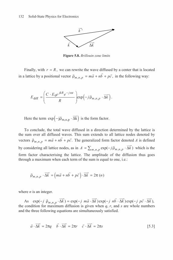
132 Solid-State Physics for Electronics
Figure 5.8. Brillouin zone limits
Finally, with ,r R we can rewrite the wave diffused by a center that is located in a lattice by a positional vector , , ,m n p ma nb pc in the following way:
0diff , ,exp
jkR j t
m n pC E e e
E j kR
.
Here the term m,n,pexp j k is the form factor.
To conclude, the total wave diffused in a direction determined by the lattice is
the sum over all diffused waves. This sum extends to all lattice nodes denoted by vectors , , .m n p ma nb pc The generalized form factor denoted A is defined
by considering all lattice nodes, as in , ,, , exp( )m n pm n pA j k which is the
form factor characterising the lattice. The amplitude of the diffusion thus goes through a maximum when each term of the sum is equal to one, i.e.:
, , 2 ( )m n p k ma nb pc k n
where n is an integer. As , ,exp( ) exp( ) exp( ) exp( ),m n pj k j ma k j nb k j pc k
the condition for maximum diffusion is given when q, r, and s are whole numbers and the three following equations are simultaneously satisfied.
2 2 2 a k q b k r c k s [5.3]
k k
'k

Reciprocal Lattices and Brillouin Zones 133
These are called Laue equations and define the point of maximum diffusion. They make it possible to determine the vector ,k which combined with
' ,k k k determines the directions of 'k for maximum diffusion.
5.4. Reciprocal lattice
5.4.1. Definition and properties of a reciprocal lattice
We can write the k vectors that verify equation [5.3] as:
,k hA kB lC [5.4]
where h, k, and l are natural integers and , ,A B C are the vectors that will be determined. To ensure k verifies Laue conditions in equation [5.3], it suffices that the , ,A B C vectors are such that:
2 0 0
0 2 0
0 0 2 .
A a B a C a
A b B b C b
A c B c C c
[5.5]
From the first column we find that A b and A c so that A is collinear to the vectorial product of ( ).b c From this we can deduce that ( ),A K b c and then by performing a scalar multiplication of both members with a the first
condition 2A a gives 2( )
.a b c
K From this we can deduce the vector A
and then by circular permutation the vectors B and ,C as in:
2b c
Aa b c
, 2c a
Ba b c
and 2 .a b
Ca b c
[5.6]
Because the dimensions of these vectors are inverse to length, they are reciprocal vectors. The property that will be defined is such that these vectors will be considered as (base) fundamental to the reciprocal lattice. It is worth remembering
134 Solid-State Physics for Electronics
that the vectors , ,A B C are only mutually orthogonal when , ,a b c are also mutually orthogonal.
Just as in a direct lattice (DL), the position of the nodes are indicated by the tips
of the vectors , ,m n p ma nb pc (where [ , , ]a b c are the base vectors of the
DL). Similarly, the vectors , ,h k lG hA kB lC (where [ , , ]A B C should therefore also be the same base vectors of the reciprocal lattice) describe the reciprocal lattice nodes.
The result is that for the reciprocal lattice given by
, ,h k lG hA kB lC [5.7]
the vectors verify the Laue conditions because according to equation [5.4] they are such that:
, ,h k lG k [5.8]
where k follows Laue conditions set out in equation [5.9]. Conversely, and in a practical sense, we can say that if a vector k is equal to
a vector of the reciprocal lattice (given by , , )h k lG hA kB lC then the vector
k verifies Laue conditions for maximum diffusion (i.e. diffraction).
5.4.2. Application: Ewald construction of a beam diffracted by a reciprocal lattice
Here we use the conditions for an elastic diffusion so that there is energy conservation between the incident and diffused waves, i.e. ' and = ’ and k k’. In equation [5.8] we saw that the condition for maximum diffusion for the wave vector is such that , ,h k lk G and in turn ' .k k k Here we thus have:
, ,' .h k lk k G [5.9]

Reciprocal Lattices and Brillouin Zones 135
From the DL we can build the reciprocal lattice [ , , ].A B C The vector k is then traced parallel to the incident ray and its end point is at a node in the reciprocal lattice. We then draw a sphere (called an Ewald sphere) of radius k and a center of origin .k The nodes of the reciprocal lattice that belong to this sphere thus make it possible to determine the 'k vectors for maximum diffusion. In effect, they are in accordance with both k k’ and , ,' h k lk k G as two nodes in the reciprocal
lattice belonging to the Ewald sphere are exactly united by the vector , , .h k lG The
diffused ray is thus parallel to , ,' .h k lk k G
5.5. Brillouin zones
5.5.1. Definition
Briefly, we can define Brillouin zones as being zones delimited by Wigner-Seitz cells in a reciprocal lattice.
5.5.2. Physical significance of Brillouin zone limits
Squaring up equation [5.9] for the maximum diffusion of a wave with wave vector k gives us:
22 2 2, , , , , ,' 2 ,h k l h k l h k lk k G k G k G
so that with k k’ (linear crystal):
2, , , ,2 0.h k l h k lk G G [5.10]
k '
G
Reciprocal lattice
Ewald sphere
Figure 5.9. Ewald sphere in a reciprocal lattice

136 Solid-State Physics for Electronics
This relation can also be written for vector , , h k lG because if , ,h k lG (as
defined by equation [5.7]) is a vector of the reciprocal lattice, then , , h k lG is also a vector of the reciprocal lattice (as it is also in accordance with equation [5.7]).
Equation [5.10] thus gives:
2, , , ,2 ,h k l h k lk G G [5.11]
so that:
2
, , , ,1 12 2h k l h k lk G G [5.12]
Figure 5.10. Tracing out Brillouin zone limits
Figure 5.10 shows a simplified 2D representation (only and BA vectors are involved) of a reciprocal lattice obtained by taking a node at origin O and using the fundamental vectors , B and C.A The , ,h k lG vector of the reciprocal lattice joins
the origin node with any other of the reciprocal lattice ( 1,0G A and
2,1 2G A B in the example given in Figure 5.10) so that the mediating plane
1,0A G
B 2,1G
( 1) ( 2)
1k
2k O

Reciprocal Lattices and Brillouin Zones 137
( ) is the segment of modulus , , .h k lG For the system shown in Figure 5.10, 1 and
2 are in fact the mediators. As shown in Figure 5.10, 1k and 2k tie O to 1 and 2,
respectively, and indeed all k wave vectors going from the origin to this type of mediator plane ( ) are in accordance with equation [5.12] which relates k to the maximum wave diffusion.
In a regular solid, electrons associated with a wave vector that has an extremity
at the plane (the Brillouin zone limit or the Wigner-Setz cell of the reciprocal lattice) undergoes the maximum diffusion. These electrons are reflected by the DL nodes (ions) and therefore cannot propagate. This is in effect the same property as that found for semi-free electrons of a wave vector that is in accordance with
ak n at the band limits.
In section 5.6.3 it is thus shown that equation [5.10] from which equation [5.12]
is derived is equivalent to the Bragg condition for maximum wave diffusion (diffraction) (presented in section 3.4.2).
5.5.3. Successive Brillouin zones
By definition, the first Brillouin zone is the smallest volume in 3D, or the smallest surface in 2D, that is generated by mediating planes created by the segments joining the origin of the reciprocal lattice with its first neighboring nodes. The second zone brings in a similar volume with the exclusion of the first Brillouin zone. This process is repeated ad infinitum.
5.6. Particular properties
5.6.1. Properties of , ,h k lG and relation to the direct lattice
Here we show that the reciprocal lattice vector , ,h k lG hA kB lC is
normal to the reticular plane (hkl) of the direct lattice and that 2
, ,, , ,
dh k lh k lG
where , ,h k ld is the inter-reticular distance between Miller index planes (hkl).
According to the definition of Miller indices, plane (hkl) goes through points M, N and P (Figure 5.9) situated in that order on the three axes x, y and z at distances
, ,K K Kh k l
from the origin (O) of the DL. K is a constant whole number. To show

138 Solid-State Physics for Electronics
that , ,h k lG is normal to the plane (h, k, l), we need to show that with two vectors in the plane its scalar product is equal to zero. This can be done by using equations [5.5] shown above. Thus we find:
, , , ,
K (hA+kB+lC)
k 2 K - 2 K = 0.
h k l h k lG HK G OK OH
Kb a
h
Similarly, we find that , , 0,h k lG KL which indicates the perpendicular
nature of , ,h k lG to the plane (hkl). If we now denote the projection of O on the plane MNP (plane (hkl)) as H, i.e.
OH goes in the same direction as , ,h k lG given the aforementioned property, and
then by making hklOH d which is the inter-reticular distance between planes
(hkl), we can calculate the scalar product , ,h k lG OM by remembering that OH is
the projection of OM on , , :h k lG
, ,, ,
, , , ,
2 ( ) 2
=
h k lh k l
hklh k l h k l hkl
KG OM hA kB lC a K
G KhdG OH G d
. [5.13]
x
y
z
MN
P
H
, ,h k lG
Oa b
Figure 5.11. Relation between , ,h k lG and the direct lattice
c

Reciprocal Lattices and Brillouin Zones 139
5.6.2. A crystallographic definition of reciprocal lattice
Crystallographers determining inter-reticular distance generally prefer to use equation [5.14] in place of equation [5.13]. Equation [5.14] relates the reciprocal lattice to the direct lattice more simply. This is because the inter-reticular distance between (hkl) planes is simply the inverse of the reciprocal lattice vector modulus (corresponding to , ,h k lG which is normal to planes (hkl)).
, ,1
.h k lhkl
G Kd
[5.14]
To obtain this equation, the base vectors of the reciprocal lattice must verify the following equations [5.15] which take the place of equations [5.5]:
1 0 0
0 1 0
0 0 1.
A a B a C a
A b B b C b
A c B c C c
[5.15]
The base vectors defined above by equations [5.6] are now redefined by the following equations [5.16] (which lose their physical significance at the Brillouin zone limits, excepting that the wave vector modulus is given by 1k in place of
the more normally used 2 ):k
,b c
Aa b c
c a
Ba b c
and .a b
Ca b c
[5.16]
5.6.3. Equivalence between the condition for maximum diffusion and Bragg’s law
Now let us show that we have an equivalence between the vectorial relation given in equation [5.11], as in 2
, , , ,2 ,h k l h k lk G G and the diffraction condition as given by Bragg (detailed in section 3.4.2). The latter describes the condition for incident rays, reflected by crystal reticular planes, to give constructive interferences.

140 Solid-State Physics for Electronics
Figure 5.12. Establishing Bragg’s law
Consider the (hkl) planes with an inter-reticular distance denoted by dh,k,l and an incident ray with a wavelength ( ) such that is the angle between the wave vector of the incident wave and the (hkl) planes. The difference in step between the reflected waves 1 and 2 (shown in Figure 5.12) is such that:
2 sin .hkld
The constructive interferences (i.e. maximum diffusion points) occur when n (n being an integer), so that:
2 sin .hkld n [5.17]
If we compare equations [5.17] and [5.11] we can see that the latter is of the form:
2, , , ,2 cos
2h k l h k lk G G
(remember from Figure 5.12 that the vector , ,h k lG is perpendicular to the (h,k,l)
plane so that , ,h k lG and k make an angle equal to 2
). Using 2 ,k we can
rewrite this equation to give:
, ,h k lG
k
= 2dhkl sin
dhkl Plan (hkl)
Incident ray Reflected ray (1)
(2)

Reciprocal Lattices and Brillouin Zones 141
, ,
(11)
22 sin
2 ( ), where is is the integer from equation [5.13]
h k l
hkl
G
n n Kd
2 sin ,hkld n
so that in effect we have derived equation [5.17] from equation [5.11]!
NOTE.– In order to be true, equation [5.17] requires that the wavelength of the rays should be a similar order of size to that of the distance (dh,k,l) between reticular planes. With dh,k,l typically being in the order of tens of nanometers, this means that the incoming rays should be X-rays.
5.7. Example determinations of Brillouin zones and reduced zones
5.7.1. Example 1: 3D lattice
To take the simplest example i.e. a simple cubic lattice, we have a b c a where a is the lattice repeat unit. The direct lattice is shown in
Figure 5.13.
Figure 5.13. Direct lattice of the simple cubic (sc) structure
As ,a b c the defining equation for the base vectors of the reciprocal lattice clearly show that .A B C
z c OO b y a x

142 Solid-State Physics for Electronics
In addition, with 3( )a b c a , i.e. the volume of the primitive unit cell of side a
and 2b c a (vector b and c being orthogonal and of modulus a), we have:
22 .
( )
b cA B C
a b c a
With the base vectors of the reciprocal lattice being orthogonal and of identical modulus 2( )
a the reciprocal lattice of the simple cubic lattice also takes on a cubic
structure (and with repeat unit 2a
in three directions).
The direct application of the Brillouin zones definition shows that the first zone (and those following) is cubic with side 2 ,
a and therefore of volume given by:
2 3.
aZBV
The geometric representations for a 2D structure are given in the following section along with a plan figure.
Finally, we can show that for such a structure, we have:
.² ² ²hkl
ad
h k l [5.18]
We have 2 2 2 2 2 2 2 2, , ( ) ,h k lG hA k B lC h A k B l C as a b c
and given the values for , ,A B C we obtain ² ² ²² ² ²
22, , 2 .h k l
a a ah k lG
Using equation [5.13] in the form 2
, ,, , ,
Gh k lh k ld makes it possible to obtain
equation [5.18] as planned.
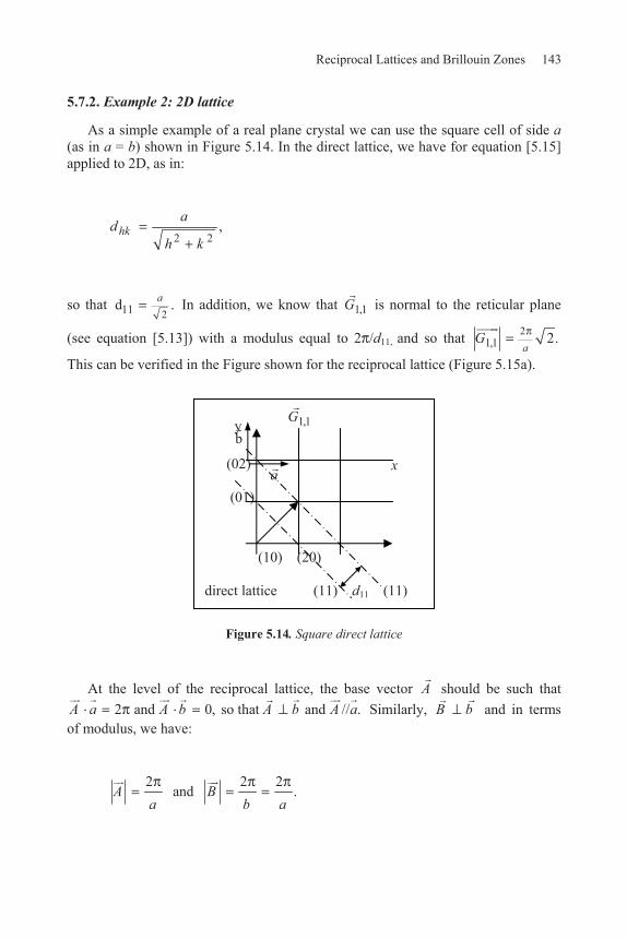
Reciprocal Lattices and Brillouin Zones 143
5.7.2. Example 2: 2D lattice
As a simple example of a real plane crystal we can use the square cell of side a (as in a = b) shown in Figure 5.14. In the direct lattice, we have for equation [5.15] applied to 2D, as in:
2 2,hk
ad
h k
so that 211d .a In addition, we know that 1,1G is normal to the reticular plane
(see equation [5.13]) with a modulus equal to 2 /d11, and so that 21,1 2.
aG
This can be verified in the Figure shown for the reciprocal lattice (Figure 5.15a).
Figure 5.14. Square direct lattice
At the level of the reciprocal lattice, the base vector A should be such that 2 and 0, so that and // .A a A b A b A a Similarly, B b and in terms
of modulus, we have:
2 2 2and .A B
a b a
(02) (01) (10) (20) direct lattice (11) d11 (11)
y
a
b
x
1,1G

144 Solid-State Physics for Electronics
Figure 5.15. (a) Reciprocal lattice of a square direct lattice;
and (b) Brillouin zones
We can deduce that: 11 ,G A B so that 2 2 211G A B
2 24 42 2 ,
a a and
2 2
1111 2
a dG where
211 .ad We also have, for example with 52,1
ad
such that 2 2 5
2121 2 .
d aG A B Given the general definition, the Brillouin
zones are represented in terms of the reciprocal lattice, as shown by the first gray zone in Figure 5.15a and the three zones in Figure 5.15b. The first zone is a square with sides equal to 2 .
a The following zones have the same dimensions. We can check this
in Figure 5.16 where we have placed the second zone into the first to give a representation of reduced zones as already used for dispersion curves (Figure 4.9).
In order to do this, we simply need to apply a translation of modulus 2a
A
with a direction and sense appropriate to each of the elements that make up the second zone (2a, 2b, 2c, 2d) in order to exactly cover the square surface of the first zone
(surface of value 2 2).
a A similar transformation can also be carried out taking the
third zone into the first, and so on. It is thus shown that in this case, the Brillouin zones (BZ) are all exactly the same size.
(b)
A
B
First Brillouin zone Second Brillouin zone Third Brillouin zone
4 /a 2 /a
1,1,1G
A 2a
a
(a)
kx
ky
B

Reciprocal Lattices and Brillouin Zones 145
Figure 5.16. Reduction of the second zone to the first by
translation of modulus 2 /a for each element (2a, 2b, 2c, 2d)
5.7.3. Example 3: 1D lattice with lattice repeat unit (a) such that the base vector in the direct lattice is a
The direct lattice with the lattice repeat unit denoted by a can be simply schematized as below in Figure 5.17.
Figure 5.17. 1D periodic lattice
The fundamental vector A of the reciprocal lattice is such that 2 ,A a and
its modulus verifies 2 .a
A
The reciprocal lattice along with the successive Brillouin zones are traced in
Figure 5.18. We can see without too much difficulty that the various Brillouin zones are of the same size (length 2 /a).
Figure 5.18. Reciprocal lattice and the Brillouin zone (BZ) of a 1D lattice
2a
2d
2c
2b
(b)
1st BZ 2a
2d
2c
2b
2a
2a
O
(a)
a a
a a O
-A = -2 /a O A = 2 /a 2A - /a first BZ /a
second BZ third BZthird ZB second BZ

146 Solid-State Physics for Electronics
5.8. Importance of the reciprocal lattice and electron filling of Brillouin zones by electrons in insulators, semiconductors and metals
5.8.1. Benefits of considering electrons in reciprocal lattices
In Chapter 4 we saw that dispersion curves can take on different forms for the various directions of the k vector, and that a plot of E = f (ki) occurs for each of the i directions that k takes on (see in particular Figure 4.4).
Working in the reciprocal lattice obviates the inconvenience of looking for more
or less arbitrary directional variations in some parameter (generally electron energy) as we now have a direct expression over all k directions, once the reciprocal lattice is plotted. This benefit becomes all the more important given that the Brillouin zones are defined and plotted within the reciprocal lattice for which the zone limits actually have a physical significance. We have seen, significantly, that these limits separate two adjacent zones where electrons can propagate, and where waves (associated with electrons) touch the zone with the extremities of their k vectors limit and are stationary, there being two electrons’ energy values separated by a gap.
Rather than filling permitted bands with electrons in accordance with the
representations given by E = f (ki) (sufficient for 1D media where there is only one kx direction to consider), it is interesting to study the electronic filling of successive Brillouin zones so as to obtain precise information on the capacity of each band to accept electrons (capacity being directly comparable over all k directions) and on the directions that are permitted for filling.
5.8.2. Example of electron filling of Brillouin zones in simple structures: determination of behaviors of insulators, semiconductors and metals
5.8.2.1. Cubic structure
5.8.2.1.1. The basics: cells in reciprocal space
Firstly, we can recall that k space can be divided into primitive cells attached to electronic states. For free electrons associated with a progressive wave, we have seen in section 2.6.2.2 that the sides of each primitive cell can be described by
2 2 2
1 2 3, ,
L L Lx y zk k k so that the volume of each cell is
383Vx y zk k k k where 1 2 3V L L L is the volume of a crystal with
sides L1, L2, L3 in direct space.

Reciprocal Lattices and Brillouin Zones 147
We should also note that the size of the primitive cell is conserved for semi-free electrons. In effect, the wave function is like a Bloch function for which the amplitude changes with x, as in: ( ) ( ).x
x
ik xk x e u x The separation of variables
means writing the wave function in the form of a product of three functions, each dependent on x, y and z. The condition due to periodic limits (that of Born von Karman) can thus be written with respect to x as:
( )( ) ( ) ( ) ( ).x x xx x
ik x ik x Lk k x xx e u x x L e u x L
As u(x) is periodic and because x xL N a if Nx is the number of atoms along
Ox, then we can deduce that 1x xik Le and in turn that 2Lx
x xk n where nx is
an integer. We therefore find that the partition in k space along Ox is with cells of dimension 2 ,
Lxxk and is identical to that for free electrons (see for example the
partition along k in Figure 3.2).
5.8.2.1.2. Filling the Brillouin zone of a simple cubic crystal structure
For a cubic crystal at the direct lattice level, and whatever the cell repeat unit in the three directions x, y, and z, the volume of the elementary cell is equal to a3. The number of primitive cells in the direct lattice of volume denoted V is therefore
3 .V
aN As each cell contains on average one node, and each node is attached to
the base of each atom, the total number of atom bases is also N. The reciprocal lattice, as we have seen in section 5.7.1, is also a simple cubic structure, while the
first Brillouin zone is a cube of side 2a
and therefore of volume 38
3 .a
We can
therefore place into this Brillouin zone a number of primitive cells equal to:
383 3
3 3 3 38
,8
a V V
k a a
where 3V
aN is precisely equal to the number of atom bases in the direct lattice.
Given that there is spin, we can place up to two electrons into each primitive cell. This means in turn that we can put two N electrons into each Brillouin zone.
148 Solid-State Physics for Electronics
So, if in the direct lattice, an atom base liberates two electrons, the first Brillouin zone is just filled by those free electrons leaving the following zone completely empty. The two zones are separated by a “gap” characteristic of the material under consideration. If the gap is in the order of 5 eV or more, then the material is an insulator, but if the value is in the order of 0.5 to 3 eV then it can be thought of as a “moderate” semiconductor.
A bivalent material (based on one atom liberating two electrons) crystallized into
a simple cubic structure is therefore an insulator or a semiconductor with a full valence band and an empty conduction band (at absolute zero). The same result would be obtained with a material that had an atomic base containing two monovalent atoms. However, if the material had an atomic base consisting of a single monovalent atom, then the first band would be half-filled so that the electrons could find themselves in free levels and be easily moved under a weak electric field: in other words the material would be a metal.
5.8.2.2. Filling Brillouin zones in a 2D square structure
That stated above for the 3D structure can equally be applied to a 2D structure. If S is the surface of a 2D crystal, the number of primitive cells that can be placed in it in a direct lattice is given by: 2 (2).
S
aN This number is equal to the number of
atom bases in the direct lattice.
The surface of all the Brillouin zones is the same, and is given by 2 2,
a as we
have seen in the scheme of reduced zones (see Figure 5.14). In the Brillouin zones we can place a number of cells equal to:
4 ²²
(2)4 ²
.² ² 4 ² ²
a S SN
k a a
Once again the number of cells in each Brillouin zone is equal to the number of atom bases. Finally, if each atom base liberates an even number of electrons (Np) then the first Brillouin zones will be full and the material will be an insulator or a semiconductor. If Np 2, then only the first Brillouin zone will be full; if Np 4, then the first two Brillouin zones will be full; if Np 6 then the first three Brillouin zones will be full; etc.
When Np is odd, then we have a metal, as in for example Np 5, and the first two
Brillouin zones are full and the third is half full.

Reciprocal Lattices and Brillouin Zones 149
5.9. The Fermi surface: construction of surfaces and properties
5.9.1. Definition
The Fermi surface is the name given to an equi-energy surface (a constant energy EF) plotted in wavenumber k space (reciprocal space). Given the Fermi-Dirac function at absolute zero, the Fermi surface separates the occupied electronic states (full orbitals) from the empty states (unfilled orbitals) at this temperature.
5.9.2. Form of the free electron Fermi surface
5.9.2.1. Establishing the form of equi-energy surfaces
In 3D, free electron energy is given by: ²2
2 2 2( ),m x y zE k k k where for a
cubic crystal of length L we have 2 ( ).Lx y zk k k n The equi-energy surface
E EF can be obtained in k space when:
2 2 2 2( ) constant .F
F x y z FmE
k k k k k
This surface is thus a sphere with a radius given by ,FE FR k where kF is
defined by the preceding relation. For a crystal shaped as a parallelepiped, and with sides given by 1 2 3L L L
the Fermi surface as given above transforms into an ellipsoid.
5.9.2.2. The form of Fermi surfaces as found in different representations
The free electron Fermi surface for a 2D crystal of a square lattice is traced in Figure 5.19a for an arbitrary electron concentration. It can be a hindrance that parts of the Fermi surface belong to the same zone, e.g. the second, and appear separated from one another. This can be avoided by using the zone schemes presented earlier. Figure 5.19b simply gives the area of the Fermi surface for the first Brillouin zone, while Figure 5.19c shows the Fermi surface in the second zone as a diagram of reduced zones (that is to say brought back as in the first zone). So that Figure 5.19c is not overloaded, only the contribution from the 2a part of the second Brillouin zone is shown (as a dotted surface). This figure can be compared with that in Figure 5.17.

150 Solid-State Physics for Electronics
Figure 5.19. (a) Circular Fermi surface for an arbitrary concentration of electrons; (b) part of the Fermi surface situated in the first zone; and (c) part of the Fermi surface situated in the second zone brought to the first zone with a contribution from 2a, shown as the dotted area. The central areas are the only ones not occupied by electrons.
5.9.3. Evolution of semi-free electron Fermi surfaces
The filling-up of electronic levels is accomplished from the bottom level up (the origin of the reciprocal lattice), and also in the corresponding equi-energy circular levels (or spheres in 3D) of which the radius (k) increases along with the filling. From a circle (or a sphere) of radius greater than 2
a (side of the square representing
the first Brillouin zone), that is to say from the limit of the Brillouin zone in the directions kx and ky (see Figure 5.13) the second zone will start filling before the first Brillouin zone is completely filled. There is an overlap between zones, as long as the potential barrier between the Brillouin zone is small.
It should be said that at this level there is a distortion caused by Brillouin zones
being defined from a periodic potential. So while the sphere (or circle in 2D) is drawn based on a hypothesis of free electrons (using the relation
²2
2 2 2( )m x y zE k k k for free electrons, the electrons are actually semi-free.
So as to have a reasoning closer to reality, we need to have an idea of the form of
the Fermi surfaces in an approximation of semi-free electrons. Qualitatively, we can state that (and this applies to a base of atoms liberating two electrons so as to fill the first zone, as is the case for bivalent atoms with one atom per base):
– if the barrier is sufficiently high, the electrons remain in the first zone (as for example, in diamond) and as shown in Figure 5.20a. First they are placed around the center and then fill the first zone up to the point where the circle (sphere) just touches the boundaries. Then they fill up the areas towards the corners, as they do not have enough energy to break the barrier to the second zone;
(a) (b) (c)
2a 2a

Reciprocal Lattices and Brillouin Zones 151
– if the barrier is not too high, electrons in the second zone are less energetic than those in the first, and now Figure 5.20b gives a better representation of the minimum energy.
Figure 5.20. Deformation of at the limit of the Fermi surface when there is: (a) a high barrier; and (b) a small barrier
Approximate constructions of semi-free electron Fermi surfaces are based on the following two facts:
i) The Fermi surface meets the limits of the Brillouin zone at a right angle In effect, the velocity of the group associated with the electron wave packet is
written as:
1,
E
gd dE
vdk dk
so that vectorially 1 grad .g kv E The vector gradk E being normal to equi-
energy lines traced in k space (reciprocal space) means that the equi-energy lines are normal to .gv
Looking at a Brillouin zone limit, and working in terms of H as shown in Figure 5.21, the wave vector y is written as: [ ] .
ka
x yk k k
The velocity (y) is given in the form: ,x yv v v and is collinear with k as *k m v (crystalline moment).
1k
(a) (b)

152 Solid-State Physics for Electronics
As /
0,x
dEdk k a
vx = 0 and ,y yv v k the velocity is directed with
respect to yk and the equi-energy lines are normal to the zone limit (limit directed
with respect to ).yk
A
B
xk
yk k
yv v
H
E = const.
Figure 5.21. Electron velocity in the band limits
ii) The crystal potential has the effect of bending the Fermi surface close to the energy extremes
In effect, within a vector k of the energy extreme (defined in the reciprocal
space by, for example, 1
1),n
nk k the energy that is developed (following MacLaurin) can be written using:
2² 12 *1( ) ( ) .k k
mE k E k
The equi-energy surfaces are spheres in #D or circles in 2D with centers at 1k
and radii defined by 2 * 1
1 .m E E
k k This explains the shape of the equi-
energy spheres at the limit of the zone.
5.9.4. Relation between Fermi surfaces and dispersion curves
As already discussed, we should consider all possible directions in the reciprocal lattice because an energy that is forbidden in one direction (kx in kx = /a) may be permitted in another (kxy again with kx = /a). This configuration is described in
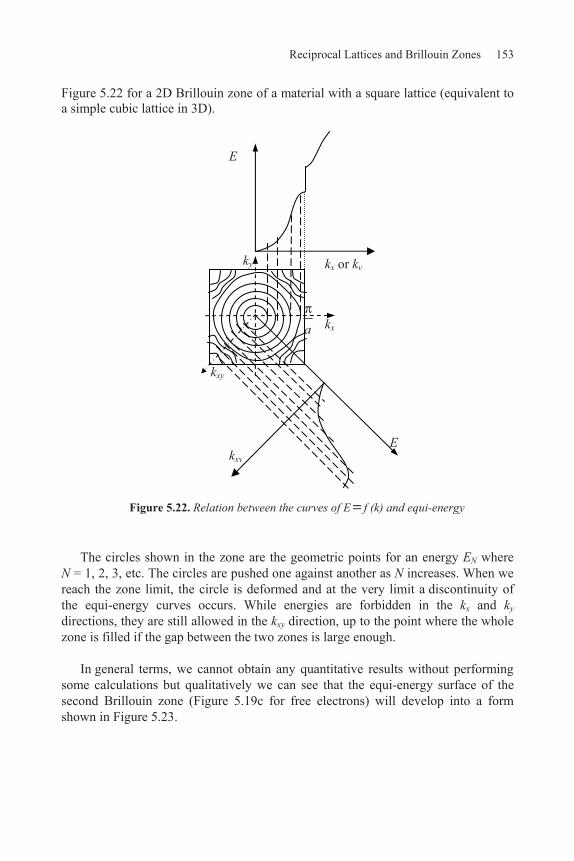
Reciprocal Lattices and Brillouin Zones 153
Figure 5.22 for a 2D Brillouin zone of a material with a square lattice (equivalent to a simple cubic lattice in 3D).
The circles shown in the zone are the geometric points for an energy EN where N = 1, 2, 3, etc. The circles are pushed one against another as N increases. When we reach the zone limit, the circle is deformed and at the very limit a discontinuity of the equi-energy curves occurs. While energies are forbidden in the kx and ky directions, they are still allowed in the kxy direction, up to the point where the whole zone is filled if the gap between the two zones is large enough.
In general terms, we cannot obtain any quantitative results without performing some calculations but qualitatively we can see that the equi-energy surface of the second Brillouin zone (Figure 5.19c for free electrons) will develop into a form shown in Figure 5.23.
Figure 5.22. Relation between the curves of E f (k) and equi-energy
E
kx or ky
kxy
E
kx
ky
a
kxy
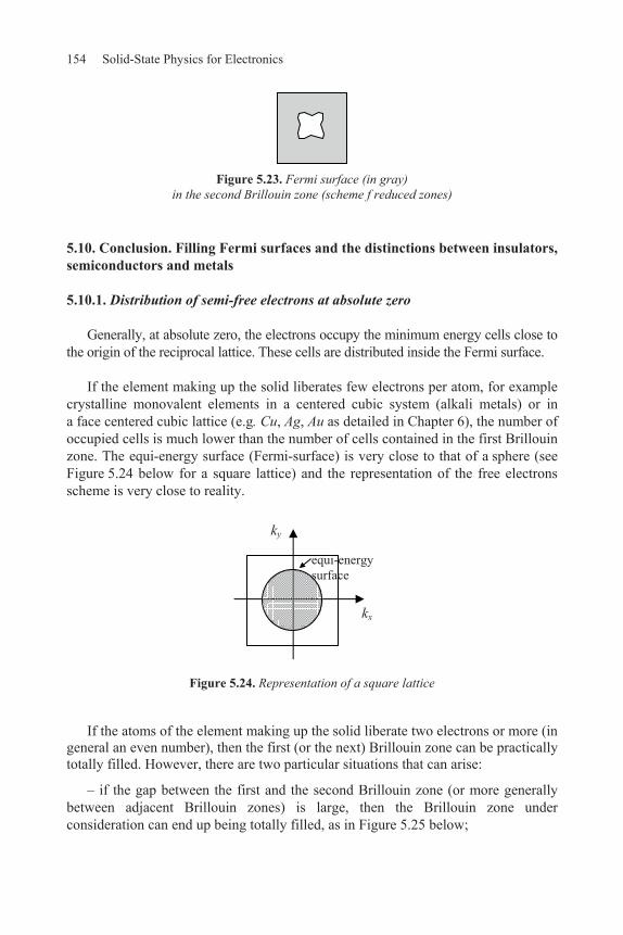
154 Solid-State Physics for Electronics
5.10. Conclusion. Filling Fermi surfaces and the distinctions between insulators, semiconductors and metals
5.10.1. Distribution of semi-free electrons at absolute zero
Generally, at absolute zero, the electrons occupy the minimum energy cells close to the origin of the reciprocal lattice. These cells are distributed inside the Fermi surface.
If the element making up the solid liberates few electrons per atom, for example
crystalline monovalent elements in a centered cubic system (alkali metals) or in a face centered cubic lattice (e.g. Cu, Ag, Au as detailed in Chapter 6), the number of occupied cells is much lower than the number of cells contained in the first Brillouin zone. The equi-energy surface (Fermi-surface) is very close to that of a sphere (see Figure 5.24 below for a square lattice) and the representation of the free electrons scheme is very close to reality.
Figure 5.24. Representation of a square lattice
If the atoms of the element making up the solid liberate two electrons or more (in general an even number), then the first (or the next) Brillouin zone can be practically totally filled. However, there are two particular situations that can arise:
– if the gap between the first and the second Brillouin zone (or more generally between adjacent Brillouin zones) is large, then the Brillouin zone under consideration can end up being totally filled, as in Figure 5.25 below;
kx
ky
equi-energy surface
Figure 5.23. Fermi surface (in gray) in the second Brillouin zone (scheme f reduced zones)

Reciprocal Lattices and Brillouin Zones 155
Figure 5.25. A totally filled Brillouin zone
– if the gap is small, or even better the bands overlap, causing the gap to disappear, then the second zone starts to fill up before the first zone under consideration is completely full.
Figure 5.26. A partially filled Brillouin zone
5.10.2. Consequences for metals, insulators/semiconductors and semi-metals
If the last occupied zone (band) is only partially filled (generally half-way) there are numerous empty cells that remain available to transport electrons under the effect of an external perturbation (for alkali metals and monovalent noble metals see the example of copper given in Chapter 6).
If the last occupied zone (band) is completely full, and if the gap with the
following zone (band) is considerable (greater than 4 or 5 eV), the electrons cannot leave the band under consideration and the material is an insulator. If the gap is relatively small (typically less than 3 or 4 eV), the insulating material at absolute zero becomes a semiconductor at ambient temperature as there are a few electrons that can pass with thermal agitation to the following zone (band) to leave holes behind (for example see germanium or silicon detailed in Chapter 6). The presence of a reasonably high gap (in the order of 5 eV such as in carbon based diamond) can nevertheless be used to furnish a material with semiconductor properties that can resist intense “flashes”, such as nuclear explosions, and can be used in devices of military importance.
kx
ky
kx
ky

156 Solid-State Physics for Electronics
If the last band can be totally filled but there is an overlap of bands, we end up with a semi-metal (for example, alkaline-earth metals have two valent electrons per primitive cell, which would be insulators except that the energy bands overlap and hence they have to a limited extent some metallic properties).
5.11. Problems
5.11.1. Problem 1: simple square lattice
Show that for a simple square lattice (2D) that kinetic energy of a free electron in a corner of the first Brillouin zone is twice as high as that of an electron situated in the middle of one side of the zone. What is the result when the lattice is cubic (3D)?
Answer For a free electron, the kinetic energy is written: ² ²
2,k
mE and we find in
2D that:
– in the middle of one side of the zone: 22² ,
axk k and 2
2
2side m a
E ;
– and at a corner of the zone: 22 2² 2
ax yk k k and 2
2
2side 2 .
m aE
We thus find that:
corner
side2.
EE
In a 3D medium, the value of Eside is unchanged while:
22 2 2
corner² ²
( ) 3 ,2 2x y zE k k k
m m a
from which in 3D: corner
side3.
EE

Reciprocal Lattices and Brillouin Zones 157
5.11.2. Problem 2: linear chain and a square lattice
1) This question concerns a linear chain made up of n identical atoms that are spaced an equal distance apart from one another so that the length of the chain L is given by L na.
a) What is the dimension of a cell in the reciprocal space?
b) How many cells can we place in each energy band?
c) Show that a 1D body is an electrical insulator (or semiconductor) at T = 0K if it carries an even number of valence electrons per atom.
2) This question carries on from the question concerning a square lattice (of side L na) that contains in all N atoms (N = n2) and each primitive cell has a side of length a.
a) Describe the direct lattice and then the reciprocal lattice.
b) Trace the first two Brillouin zones. Indicate the maximum number of electrons that can be placed in the first and the second zone. Conclude.
3) The atoms in this question are bivalent.
a) Sketch the scheme of the energy bands for semi-free electrons: E = f (k1,0) and E = f(k1,1) (where kij designates the wavenumber in the direction [i, j]).
b) Point X designates the middle of the side of the square that is the first zone. Point M is at the summit of the same square. The modulus of the wave vectors have their ends at X and at M and are denoted by kX and kM. When k = kX, the corresponding energies are denoted E(XC) for the bottom of the conduction band and E(XV) for the summit of the valence band. In addition E(XC) – E(XV) = w1,0 and is the energy gap in the direction [1, 0].
Similarly, when k = kM, the energy is denoted E(MC) for the bottom of the conduction band and E(MV) for the summit of the valence band, with E(MC) – E(MV) = w1,1 being the energy gap in the direction [1, 1].
What relations are there between E(MV) and E(XC) when the material that is made up of bivalent atoms is at T = 0K an insulator or a conductor?
c) Within the last hypothesis, detail the appearance of the Fermi and first Brillouin zone surfaces.
4) Numerical analysis:
w1,0 = 4 eV, w1,1 = 2 eV,

158 Solid-State Physics for Electronics
² ²4.2
2 ²m a eV (when a 0.3 nm).
Is the material a conductor or insulator at absolute zero?
Answers
1)
a) For a direct space of dimension L, the dimension of one cell in reciprocal space is given by 2 ,
Lk where L = na, with n making p the number of atoms
that go into a linear chain.
b) For a periodic system of period a, an energy band is localized between
ak and .
ak Its width is thus given by 2 ,
a and inside it can be placed
2
2a
L
La
n cells.
c) With the possibility of placing two electrons per cell, we can thus place 2n electrons per band (each band being the same size, as in 2
a) in all. If the atoms each
liberate an even number (Np) of valence electrons, then the number of bands that the nNp of electrons that will be able to fill at absolute zero (temperature at which the Fermi function is equal to one when E < EV < EF) will be:
– 1 band if Np = 2,
– 2 band if Np = 4,
– 3 band if Np = 6,
– etc.
with, in all cases, a last band that is completely full. The material is thus an insulator if there is a large gap and a semiconductor if the gap is small (i.e. less than 3 eV).
2)
a) The problem is now 2D with a square direct lattice of side L = na and N = n2 atoms in all.

Reciprocal Lattices and Brillouin Zones 159
Figure 5.27. Sketches for Answer 2: square direct lattice (left) and the base vectors on the reciprocal lattice (right)
The base vectors of the reciprocal lattice are such that 2 ,a
A B where
0,A b so that A b and similarly .B a
b) The first two zones shown above are of the same surface (as detailed in
many university courses on how to use reduced zones) and equal to 2 2.
a The 2D
cells in reciprocal space are of a size given by 4 ²²
,Lx yk k and therefore in
each zone we can place 2 2 ²2 2
²²L
aa Ln N cells, which is equal to the
number of atoms in the system. With two electrons per cell, we can put in 2N electrons per zone. If the N atoms have a valency of two, they will liberate 2N electrons that can only just fully fill the first zone. This complete filling will only occur if the barrier between the two zones is sufficiently high to push electrons to the corners at the end, and will result in insulating (or semiconducting) behavior. If the atoms have an odd number valency (monovalent), the last band to be occupied will be half-full in respect of equi-energy circles with a maximum radius of
kf =2 * .m EF If kf < ,
a then the circles do not reach the second Brillouin zone, the
bands will not overlap and a metal is formed. If kf > ,a
there is a risk of two bands
overlapping with the ensuing formation of semi-metallic behavior.
L = na
L = na a
b
a
a
a
a
first BZ
second BZ
2A
a
2B
a
direction [10]
direction [11]
X
M2
a

160 Solid-State Physics for Electronics
3) The atoms are bivalent, and when the extremity of a wave vector touches the zone limit, the energy levels of the different bands need to be compared.
Figure 5.28. Diagram of the band scheme with respect to the directions [1,0] and [1,1]
a) Schematically, and from the perspective of the bands, the representation above shows the two principal directions [1, 0] and [1, 1]:
– If E(MV) < E(XC), the first band and hence the first Brillouin zone is completely filled with up to 2N electrons. Being completely filled it is thought of as an insulator or semiconductor with a gap given by: E(XC) E(MV) = wG.
– If E(MV) > E(XC), the second band starts to fill before the first band is completely full. The two bands are incompletely filled and have overlapping energy bands – the materials is semi-metallic (no resultant gap). Within the free electron theory, the Fermi surface takes on the shape shown below as a dashed line circle. For these semi-free electrons, the circle becomes deformed as shown in section 5.9.3.
Figure 5.29. Incomplete bands with overlapping energy levels (as when E(MV) > E(XC))
First BZ
Fermi surface of free
electrons
a
2a
E
X
k1,0 k1,1
M
MV
MC
XV
XC
MV
w1,0
w1,1 wG

Reciprocal Lattices and Brillouin Zones 161
These ideas can be extended to 3D materials and can explain how Mg, Be and Pb are metallic, while Si, Ge and Se are semiconductors.
Given the relationship that exists at the band limit, we can quantitatively write that for the preceding two inequalities in a square lattice:
2.
X
M
ka
ka
Knowing w1,1 and w1,0, and hence ² ²2 ²
4.2m a
eV, we can discover whether or
not the bivalent material is an insulator or a semi-metal.
With w1.0 = 4 eV and w1,1 = 2 eV we have:
2 11 1111
² ² 2 ²( )
2 2 2 ² 22
4.2 2 7.4 eV2
Vw w
E M km m a
2 10 1010
² ² ²( )
2 2 2 ² 24
4.2 6.2 eV.2
Cw w
E X km m a
Thus E(MV) > E(XC), which implies a semi-metallic character. NOTE.– In the numerical calculation, there is:
2340.3nm 19
/ 30 20
6.62 10² ² ² 1 16.76 10 J,
2 ² 8 ² 8 0.9 10 9 10
aa
xhE
m a m a
or rather:
19
/ 196.76 10
eV 4.227 eV.1.6 10
aE

162 Solid-State Physics for Electronics
5.11.3. Problem 3: rectangular lattice
This problem concerns a 2D material in a rectangular lattice that has the following parameters: the primitive cell is such that a = 2 Å and b = 4 Å; the lengths of the real crystal are L1 = N1a and L2 = N2b; and the number of nodes (where there are placed A-type atoms) is given by N N1N2. We assume that the base is defined by two atoms: atom A placed at (0, 0) and atom B placed at (1/4, 1/4). The outer layer electrons dispersion relationship (valence electrons) follows that of the semi-free electrons theory. That means for a given direction [m, n] the curve E = f (k) follows that of free electrons (of energy E) except when in the vicinity of discontinuities, where the energy for the first discontinuity can be written as:
Em,n = Em,n wm,n/2 (discontinuity amplitude is wm,n where in this case wm,n > 0).
In terms of notation:
EV[m, n] = E m,n = Em,n – wm,n/2 and EC[m, n] =E+m,n = Em,n + wm,n/2.
And we have ² 2 3.82 eVm Å2.
1) Show:
a) the direct lattice with base vectors that are written as xa ae and yb be ;
b) the reciprocal lattice and the base vectors that we will determine the first two Brillouin zones and their geometric forms.
2) Give the expression for the energy at zero order in k space at the first point of discontinuity that appears with the first-order approximation (semi-free electrons) in:
a) the direction [1, 0];
b) the direction [0, 1];
c) the direction [1, 1].
In the figure also sketch the dispersion curves [E = f (km,n)] for semi-free electrons with various energy levels, namely: w1.0 = 1.5 eV; w0.1 = 2 eV; and w1.1 = 1 eV.
3) This question studies the filling of Brillouin zones at absolute zero. Each AB atomic basis set liberates two electrons that are semi-free.
a) Indicate the number of electrons that the first Brillouin zone can accommodate.
b) What inequality exists between the parameters wm,n and a and b of the direct lattice cell so that a crystal is an insulator?

Reciprocal Lattices and Brillouin Zones 163
4) Applying the result from above.
a) The values that are given are: w1,0 = 1.5 eV; w0,1 = 2 eV; w1,1 = 1 eV; 2 /2m = 3.82 eV Å2. Determine whether or not the crystal is an insulator or a
conductor at absolute zero.
b) Now the material is a conductor at absolute zero. Schematically show the form of the equi-energy curve EF (corresponding to the Fermi level for which the significance of absolute zero should be noted).
5) From now on B is placed at (1/2, 1/2) and the atoms A and B are chemically identical. The direct lattice can now be thought of as part of a centered rectangle.
a) Show the geometric form of the direct lattice with its new primitive cell (along with the two fundamental vectors and their components).
b) Give the base vectors of a traced reciprocal lattice and give its structure.
c) Trace the first Brillouin zone and show its geometric form.
d) We will assume that the A atoms are monovalent. From the determination of the Fermi circle line, show if the material is a conductor or an insulator.
e) The A atoms are now supposed to be bivalent. Indicate the new position of the Fermi circle. From this can it be deduced, using the given data, whether the material is an insulator or a conductor?
Answers
1)
a)
a
b
� �
� �
� �
� �
� �
� �
�
�
�
� Atom B (1/4, 1/4)
Atom A (0,0)
o
o
, with = 2
, with = 4
x
y
a ae a A
b be b A
Figure 5.30. Direct lattice with base vectors
b) The base vectors of the reciprocal lattice are such that 2 ,a
A with
0,A b so that ;A b and similarly, 2 ,b
B with 0,B a we have .B b

164 Solid-State Physics for Electronics
Figure 5.31. Reciprocal lattice with base vectors
In the figure it can be seen that the two upper and lower triangles are empty. They do not belong to the second Brillouin zone but to those at higher numbers.
2) The answer can be given as:
a) In the [1, 0] direction (which is that of ):A k = k1,0 = ;a
and we thus have a = 2 Å
201,0
² ²1.57 3.82 9.43 eV
2 4E k
a m a
b) In the [0, 1] direction (which is that of ):B k = k0,1 = ;b
and we thus have b = 4 Å
201,0
² ²0.79 3.82 2.36 eV
2 16E k
b m b
c) In the [1, 1] direction (which is that of 1,1):G k = k1,0 = ;a
and
01,1
2 2
1 / ² 1 / ² 1.76
² 5 ² 3.82 11.78 eV.
2 16
E k a b
m a b
1 – c: first BZ second BZ
1,1OG A B and
1,11 1
² ² 2² ²
OG A Ba b
[1, 1]
A
B
[1, 0]
[0, 1]
1,1OG
a
b

Reciprocal Lattices and Brillouin Zones 165
Figure 5.32. Band structures in the directions: a) [1,0];b) [0,1]; c) [1,1]
3) Filling Brillouin zones:
a) Each atomic base liberates two electrons and in the direct lattice we have on average one base per rectangular cell (four bases are attached to each cell, and each base is shared between four cells so there is on average one atom base per cell). If S is defined as the surface of the direct lattice, then S = L1L2 = N1N2ab. With each cell having the surface ab, we find S/ab = N1N2 = N which is the number of atoms (or nodes) in the direct lattice.
In the reciprocal lattice, the surface of the first Brillouin zone is given by
4 ²2 2* .aba b
S The surface of a primitive cell is such that x yk k
4 ²2 2
1 21 2,
N N abL L so that in the first Brillouin zone we can place
4 ² 4 ²
1 21 2ab N N ab
N N N cells. Being able to place two electrons per cell, the first
Brillouin zone is totally full with 2N electrons. As a consequence, the first Brillouin zone may receive 2N electrons freed by the base of N atoms.
b) In order to determine if the material is an insulator/semiconductor or semi-metallic, we need to know if the bands are overlapping or not. This means finding
w1,0 = 1,5 eV
w1,1 = 1 eV
w0,1 = 2 eV
1,0k 0,1k 1,1k
a
b
1 1² ²a b
E1,0
E0,1
E°1,1
E E E
EV[1, 1]
EC[0, 1]
EV[1,0]
EC[1, 0]
a) c) b)

166 Solid-State Physics for Electronics
out whether or not the band filling in the direction [0, 1] (corresponding to the lowest energies) of the second band starts before filling of the first band in other directions is complete.
So that there is no overlapping whatsoever, the lowest level of the conduction
band should not be filled before the highest level of the valence band is complete. For this to happen, there should simply be no overlap between the directions [0, 1] and [1, 1] that correspond, respectively, to the lowest and highest energy directions.
In order to have the insulating (or semiconducting) state, we therefore need to find:
EV[1, 1] < EC[0, 1],
so that:
E 1,1 = E1,1 – w1,1/2 < E+0,1 = E0,1 + w0,1/2.
This condition can also be written as:
w0,1 + w1,1 > 2(E1,1 – E0,1) =2 ² 1 1 1
² ² ,2 ² ² ²m a b b
so that:
w0,1 + w1,1 >² ²
.²ma
4) Numeric application:
a) With w0,1 = 2 eV and w1,1 = 1 eV, we have: w0,1 + w1,1 = 3 eV.
With a = 2 Å and 2 /2m = 3.82 eV Å2, we can deduce:
² ²²ma
= 18.85 eV, from which w0,1 + w1,1 = 3 eV < ² ²
²ma= 18.85 eV.
The material is therefore semi-metallic.
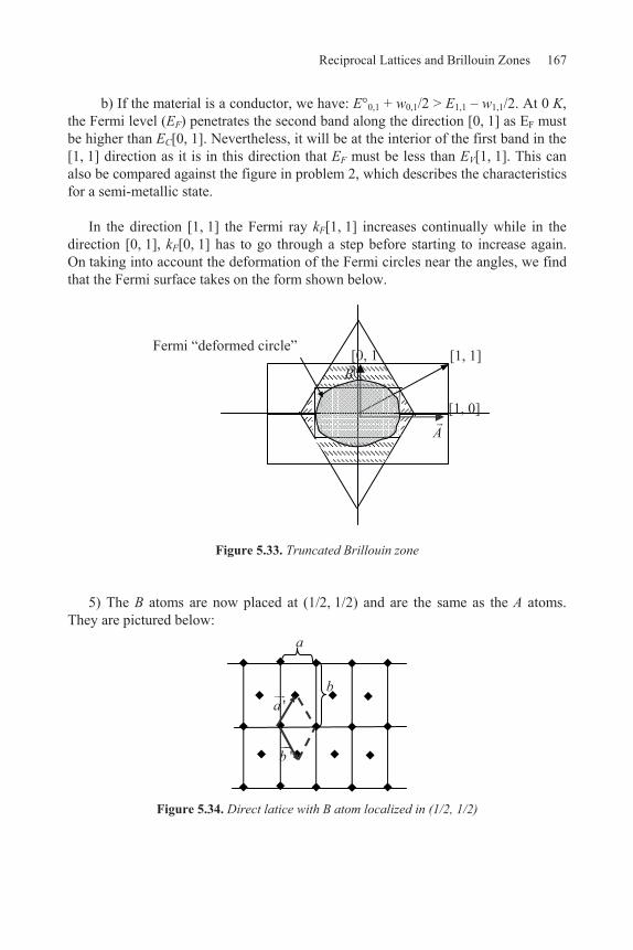
Reciprocal Lattices and Brillouin Zones 167
b) If the material is a conductor, we have: E°0,1 + w0,1/2 > E1,1 – w1,1/2. At 0 K, the Fermi level (EF) penetrates the second band along the direction [0, 1] as EF must be higher than EC[0, 1]. Nevertheless, it will be at the interior of the first band in the [1, 1] direction as it is in this direction that EF must be less than EV[1, 1]. This can also be compared against the figure in problem 2, which describes the characteristics for a semi-metallic state.
In the direction [1, 1] the Fermi ray kF[1, 1] increases continually while in the
direction [0, 1], kF[0, 1] has to go through a step before starting to increase again. On taking into account the deformation of the Fermi circles near the angles, we find that the Fermi surface takes on the form shown below.
Figure 5.33. Truncated Brillouin zone
5) The B atoms are now placed at (1/2, 1/2) and are the same as the A atoms. They are pictured below:
Figure 5.34. Direct latice with B atom localized in (1/2, 1/2)
b
a
'a
'b
[1, 1]
A
B
[1, 0]
[0, 1]
Fermi “deformed circle”

168 Solid-State Physics for Electronics
a) The direct lattice is thus a centered rectangle. The primitive cell is rhombus shaped, and a base vector for the vectors such that:
/ 2 / 2' and ' .
/ 2 / 2a a
a bb b
The surface of the elementary cell is:
1' 4
2 2 2 2a b a b
s ,
and the number of elementary cells that we can place in a sample of the surface is given by S = L1L2 = N1N2 ab = Nab and is equal to
'2 .S
sN As each rhombic
primitive cell contains on average one atom (four atoms shared between four adjacent cells), a sample of the surface S contains 2N atoms in all.
NOTE.– If instead of considering the preceding primitive cell, we look at a centered rectangular cell, the surface is now given by s = ab. In the sample given by the surface S = L1L2 = N1N2 ab = Nab, we can place S/s = N rectangular cells. As this cell contains on average two atoms per cell (one atom at the center of the cell and on average one atom at the top of the cell, with four atoms at four summits being shared between four adjacent cells), we can place a total of 2N atoms in the sample surface S, i.e. a result identical to the preceding case.
b) The base vectors of the reciprocal lattice, '* XY
A and '* VW
B are such that they should agree with:
'* ' 2 (1) '* ' 2 (2)2 2 2 2
'* ' 0 (3) '* ' 0 (4)2 2 2 2
a b a bA a X Y B b V W
a b a bA b X Y B a V W

Reciprocal Lattices and Brillouin Zones 169
We thus have a system based on four equations with four unknowns (X, Y, V, W). So:
(1) + (3) X a = 2 X = 2 /a (1) (3) Y b = 2 Y = 2 /b (2) + (4) V a = 2 V = 2 /a (2) (4) W b = 2 W = 2 /b
As a consequence, the elementary cell of the reciprocal lattice has the same conformation as the reciprocal lattice cell. The reciprocal lattice is also a centered rectangle. Mathematically, we in effect need only to equate the components of '*A and '*,B as in 2 /a = c/2 and 2 /b = d/2, to see that the fundamental vectors '*A and '*B have the same components as the fundamental vectors 'a and 'b from the direct lattice when:
/ 2 / 2'* and '* .
/ 2 - / 2c c
A Bd d
c) The first Brillouin zone takes on a rhombic shape – shown as a gray surface in the figure below.
Figure 5.35. Rhombic-shaped first Billouin zone (gray area)
2 a
2 bA '*
'*B
C D
K
kF
2 / 2 /
'* and '*2 / -2 /
a aA B
b b

170 Solid-State Physics for Electronics
We can state that:
1 1OC 2
a² b²;
and its mediator delimits (in the direct lattice of the centered rectangle) the first Brillouin zone, and is identical to that which delimits the second Brillouin zone of the direct lattice of the preceding example based on a simple rectangle. The same is true for OD = 2.2 /b and its mediator.
We can immediately conclude that the surface of the first Brillouin zone is the
centered rectangular lattice is equal to the sum of the surface of the first Brillouin zone and second Brillouin zone of the preceding simple rectangle lattice.
d) As seen in problem 5a where there were 2N electrons to place, in the direct lattice if the A type atoms are monovalent, we have 2N atoms to place that take up
the reciprocal space of N cells on a surface given by: 4 ²2 2
1 2.
NabL L
These cells should be spread throughout the Brillouin zones with the first zone
being filled first, it having dimensions given by:
2 21.57
4 4OL
bÅ-1
2 21 2 2 1 11.76
2 ² ²OK
a b a b Å-1
The line detailed by kF of the Fermi circle, at the interior of which are placed all the 2N electrons of the N cells if the line is inside the Brillouin zone is such that
4 ²2 (Surface of a cell) .abFk N From this can be deduced that Fk
24
2 1.26
ab
ab Å-1.
The Fermi circle thus appears smaller than the smallest dimension (here along
OL) of the first Brillouin zone so that all the electrons can be placed inside the Fermi circle while maintaining empty cells in all directions. The material is therefore a conductor.

Reciprocal Lattices and Brillouin Zones 171
e) If the A atoms are divalent, we have 4N electrons to place into 2N cells, and
the Fermi circle must therefore follow: 8 ²4 ²2 2 ,abNabFk N so that
24
22 1.78
ab
abFk Å-1. This time, kF > OL and even kF > OK, so the Fermi circle
reaches the second zone and what remains to be known is what happens at the points L and K:
– either there is little or no potential barrier and the second zone starts to be populated before the first is completely full. The material is thus a semi-metal;
– or there is a high barrier that displaces electrons into the corners of the first zone and we thus need to know if we can just fill the first zone of the rectangular center, in which case the material would be an insulator.
Taking the representation for the Brillouin zone from problem 1b, it is possible
to see that with the simple rectangular structure we can use the first zone’s scheme of reduced zones for the second zone, which has the same surface. The figure below shows how part (1) of the second zone can be placed into the first. The same can be done with other parts of the second zone, as for example the surfaces of small triangles t1 and t’1 are identical. The result is that we can place, in all, 2 × 2N electrons, or rather, 4N electrons in the first two Brillouin zones of the centered rectangular structure. This is just the number of electrons liberated by the bivalent A atoms. In effect, the material is an insulator.
Figure 5.36. Diagram of the reduced zones showing that first and second zones are of the same area
[1, 1]
A
B
[1, 0]
[0, 1]
1,1OG
a
b
(1)
(1)
t1
t’1

This page intentionally left blank

Chapter 6
Electronic Properties of Copper and Silicon
6.1. Introduction
This chapter is mostly concerned with the face centered cubic (fcc) structure that is taken up by a large number of crystalline elements, such as aluminum, nickel, copper, silver, calcium, neon, argon and krypton. In addition, we find that the elements in column IV of the periodic table, silicon and germanium, crystallize in the same form as diamond carbon. In this structure, half of the atoms are in the same environment as those in a fcc structure. The other atoms are also in a fcc lattice that is displaced with respect to the former lattice by a quarter cell unit in the direction [1,1,1]. The two types of atoms differ simply in their orientation with respect to their bonds with their nearest neighbors.
Copper and silicon are both standard bearers in their respective classes of metals
and semiconductors. Given their industrial and academic importance, it is easy to see why the study of their crystalline structures in order to understand their electronic properties is so crucial.
6.2. Direct and reciprocal lattices of the fcc structure
6.2.1. Direct lattice
The fcc structure (side d) is shown in Figure 6.1. Two forms of unit cell can be constructed:
i) A rhombohedric cell based on the vectors , ,a b c joining the origin O to the center of the faces of the cube.

174 Solid-State Physics for Electronics
The component of the , ,a b c vectors on the x, y, z axes are:
/2 /2 0
/2 0 /2 0 /2 /2
x y za d d
b d dc d d
The rhombohedron is the smallest cell possible; it is therefore called the primitive cell and has, on average, one node per cell (a node for each of the eight points of the rhombohedric cell, with each being shared with eight other rhombohedric cells).
ii) A cubic cell with the base vector being vectors , ,A B C (from the d
components respectively along the x, y, z axes) with the nodes at the summit of the cell and at the center of each d face side. This fcc cell contains, on average, four nodes per cell. There are eight nodes at the summit of each face that are each shared with eight other cells and that contribute, on average, one node per cell. However, there are also six nodes at the center of six faces that are each shared between six faces and therefore bring an extra 6/2 = 3 nodes per cell.
With a total of four nodes per cell, the centered cubic cell is four times larger
than the rhombohedric primitive cell.
a
b c
dx
z
O A
C
B
Figure 6.1. Fcc structure

Electronic Properties of Cu and Si 175
6.2.2. Reciprocal lattice
6.2.2.1. Base vectors deduced directly from the direct lattice
Using the primitive cell in the direct lattice as a starting point, the base vectors
, ,A B C of the reciprocal lattice are such that, for example with ( , , )
* 2 ,b ca b c
a we
have:
²4²
4²
4
d
db c
d
and 3
( , , )8
da b c a b c ,
so that:
3² 4 2
24
2*
2
ddd
ad
d
Finally, by a circular permutation, we find the components of the three base vectors of the reciprocal lattice:
2 2 2
*
2 2 2*
2 2 2*
x y z
ad d d
bd d d
cd d d

176 Solid-State Physics for Electronics
and the modules of these vectors are such that (see Figure 6.2):
2 2 22 2 2 2* 3 * *a b c
d d d d
The vectors of the reciprocal lattice are in the form * * *, ,G ha kb lch k l ,
and the nodes closest to the origin are given by the vectors *1,0,0*0,1,0*0,0,1
G a
G b
G c
. The Brillouin
zones, which are in themselves difficult to geometricly construct, can be traced from the mediating planes of the vectors denoted *,a *,b * .c An additional simplification is made by changing the base.
6.2.2.2. Changing base in a reciprocal lattice
A new base can be more easily constructed in a reciprocal lattice by using the new base vectors given by:
* * *
* * *
* * *
A a b
B a c
C b c
In effect, the vectors *,A *,B *C make up a base as they correspond to the maximum number of linear vectors (equal to three). To confirm this property, we can create a linear combination given by 1 2 3* * *,μ A μ B μ C and show that if
1 2 3* * * 0,μ A μ B μ C then μ1 = μ2 = μ3 = 0. Given the definition of *,A
*,B *,C the linear combination gives:
1 2 3* * * * * * 0μ a b μ a c μ b c
so that:
1 2 1 3 2 3* * * 0.a μ μ b μ μ c μ μ
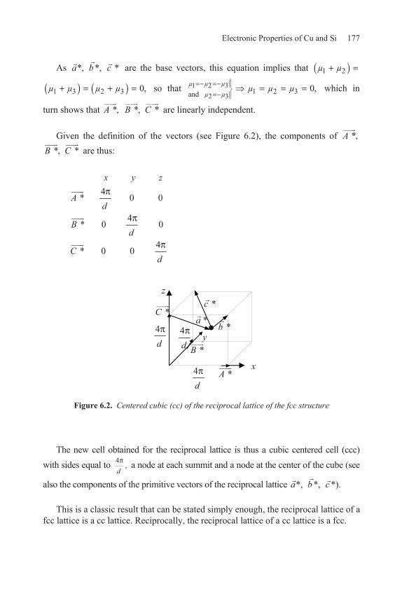
Electronic Properties of Cu and Si 177
As *,a *,b *c are the base vectors, this equation implies that 1 2μ μ
1 3 2 3 0,μ μ μ μ so that 1 2 3 2 3
1 2 3and0,μ μ μ
μ μμ μ μ which in
turn shows that *,A *,B *C are linearly independent. Given the definition of the vectors (see Figure 6.2), the components of *,A
*,B *C are thus:
4
* 0 0
4* 0 0
4* 0 0
x y z
Ad
Bd
Cd
Figure 6.2. Centered cubic (cc) of the reciprocal lattice of the fcc structure
The new cell obtained for the reciprocal lattice is thus a cubic centered cell (ccc)
with sides equal to 4,
d a node at each summit and a node at the center of the cube (see
also the components of the primitive vectors of the reciprocal lattice *,a *,b *).c This is a classic result that can be stated simply enough, the reciprocal lattice of a
fcc lattice is a cc lattice. Reciprocally, the reciprocal lattice of a cc lattice is a fcc.
x
z
y
4d
4d
*A
*B
*C *a
*b
*c
4d

178 Solid-State Physics for Electronics
6.3. Brillouin zone for the fcc structure
6.3.1. Geometric form
In the reciprocal lattice, the closest nodes to the origin are localized at:
six coordinate points 4 ,0,0 ,d
40, ,0 ,d
40,0, ,d
situated in the six
directions normal to the planes [1,0,0], [_1 ,0,0], [0,1,0], [0,
_1 ,0], [0,0,1], [0,0,
_1 ].
The vector of the reciprocal lattice 1,0,0G normal to the planes [1,0,0] is such that
1,0,0 *G A , with 41,0,0 d
G ;
eight cube centers from the combinations of 2 2 2, ,d d d
, and situated in the
eight directions [1,1,1] (normal to planes [1,1,1], [_1 ,1,1], [1,
_1 ,1], [1,1,
_1 ], [
_1 ,
_1 ,1],
[_1 ,1,
_1 ], [1,
_1 ,
_1 ], [
_1 ,
_1 ,
_1 ]). The vector of the reciprocal lattice normal to planes
[1,1,1] and with an extremity at the center of the cube (in the first octant) is the vector:
.* * *1,1,1
2 2 2 2
G A B C
Its module is such that:
22 2 21,1,12
2 2 23G
dd d d
[100]
[010]
[001]
[111]
2,0,0
d
, ,d d d
Figure 6.3. First Brillouin zone of the fcc structure
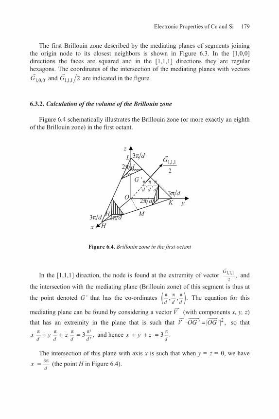
Electronic Properties of Cu and Si 179
The first Brillouin zone described by the mediating planes of segments joining the origin node to its closest neighbors is shown in Figure 6.3. In the [1,0,0] directions the faces are squared and in the [1,1,1] directions they are regular hexagons. The coordinates of the intersection of the mediating planes with vectors
1,0,0G and 1,1,1 2G are indicated in the figure.
6.3.2. Calculation of the volume of the Brillouin zone
Figure 6.4 schematically illustrates the Brillouin zone (or more exactly an eighth of the Brillouin zone) in the first octant.
In the [1,1,1] direction, the node is found at the extremity of vector 1,1,1 ,2
G and
the intersection with the mediating plane (Brillouin zone) of this segment is thus at
the point denoted G’ that has the co-ordinates , , .d d d
The equation for this
mediating plane can be found by considering a vector V (with components x, y, z) that has an extremity in the plane that is such that 2' | '| ,V OG OG so that
d dx y ²
,²
3d d
z and hence .3d
x y z
The intersection of this plane with axis x is such that when y = z = 0, we have
3d
x (the point H in Figure 6.4).
Figure 6.4. Brillouin zone in the first octant
x
y
z
3 d
3 d
3 d
2 d
2 d
2 d
1,1,1
2
G
H
L
K
, ,'d d d
G
O
MH’

180 Solid-State Physics for Electronics
Similarly, the intersection between axes y and z occurs, respectively, at 3d
y
and 3d
z (indicated as points L and K, respectively, in Figure 6.4). The points
situated at (2 ,0,0),d (0, 2 ,0),d (0,0,2 )d correspond for their part to the intersectional points at the x, y and z axes on the Brillouin surfaces, which were obtained as mediating planes in the [100], [010] and [001] directions.
The volume V ' of the first Brillouin zone of the first Brillouin zone in the first octant thus takes on the form V ' = v – 3v1, where v is the volume enclosed by three axes denoted (Ox, Oy, Oz) and the plane defined by the intersectional points HKL, and v1 represents each of the small triads at the point H, K and L of the bases clipped off in Figure 6.4. It is the removal of these pyramids that result in the truncated sides of the Brillouin zone. We thus find
– 1 3 33
21, where and
2d dv S h h S so that
3932d
v ;
– 131 1 1,v S h where 1 d
h and 12
21 d
S so that 3
,361d
v or rather,
3.3213
dv
We thus find that 34
,31' 3d
V v v and that the total volume of the sliced
octahedron, and therefore also of the first Brillouin zone is given by:
3
332
8 'V Vd
6.3.3. Filling the Brillouin zone for a fcc structure
If V0 is the volume of the starting crystal (i.e. in direct space), then the number of (fcc) cells with a volume given by 3d and containing an average of four nodes is
given by 0 .3V
d In direct space we therefore have 0
34V
dN nodes.
The volume of a cell in reciprocal space is 38
.0V
In the volume V of the Brillouin
zone of the fcc structure, we can therefore place:
Electronic Properties of Cu and Si 181
38
0
30 0
3 3 332 4
8V
V V VN
d dcells
that is, the same number as there are nodes in the direct space.
Being able to place two electrons per cell into the reciprocal space means that the fcc Brillouin zone structure will be filled with 2N electrons. However, this will only happen if the set of atoms (attached to each node) each liberate an even number of electrons.
6.4. Copper and alloy formation
6.4.1. Electronic properties of copper
The atomic number (Z) of copper is 29. Its electronic configuration is [Ar] 3d10 4s1. It is thus a mono-valent atom and therefore its fcc lattice carries N nodes on which are located N atoms that altogether liberate N electrons. The first Brillouin zone is thus half-filled meaning that copper is a metal.
We can also note that silver (Z = 47) and gold give rise to the same behavior. Their electronic configurations are, respectively, [Kr] 4d10 5s1 and [Xe], 4f14 5d10 6s1
(Z = 79).
The formation of alloys of copper with other more electronically rich elements is of particular interest given that copper has a Brillouin zone that is only half-full.
6.4.2. Filling the Brillouin zone and solubility rules
6.4.2.1. Filling the Brillouin zone and the consequences
At absolute zero, electrons occupy the minimum energy cells (starting from the origin of the reciprocal lattice) and are distributed inside the interior of the Fermi surface.
For the mono-valent elements (notably Cu, Ag, Au) that are crystallized in fcc structures, the number of cells occupied is considerably smaller than the number of cells that can be placed in the first Brillouin zone. The external surface of the distribution of full cells is very close to a sphere, and the scheme that represents the free electrons is very close to reality.

182 Solid-State Physics for Electronics
In contrast, if the element is richer in electrons, for example if it is divalent, then the first zone can be filled. However, as discussed in Chapter 5 for an equi-energy sphere that is tangential to the zone limit, there are two situations that can arise:
i) if there is a gap between the first and second zones, then the first zone fills up and the material exhibits insulator/semiconductor properties; or
ii) if the gap is small, then the second zone can start filling up before the first is completely filled, and this results in a semi-metallic behavior.
Thus, these two scenarios are separated by the point at which the electrons are just able to fill the sphere within the first Brillouin zone. The position of the equi-energy sphere, at a tangent to the zone limit, is important when evaluating the formation of alloys.
6.4.2.2. Conditions for alloy formation: the Hume-Rothery rules
6.4.2.2.1. Conditions for alloy formation
In order for alloys to be formed, the diameters of the atoms should be very close to one another, or otherwise a disparity in electrons can make it very difficult to form a solid solution. An excessive number of electrons can, however, make alloy formation quite easy. For example, mono-valent copper is only slightly soluble (1%) in bivalent zinc (Z = 30) which has the electronic structure [Ar] 3d10 4s2. But zinc is highly soluble in copper (up to 1/3 zinc and 2/3 copper). Similarly, copper is insoluble in silicon (valency of four), whereas silicon can be placed into copper (up to 6%).
Figure 6.5. (a) Variation in the maximum energy of n(E) and denoted as Em;
(b) scheme showing how the greatest number of cells filled by electrons with a given energy E is obtained with an equi-energy sphere that is tangential to the Brillouin zone
In addition, we can note that the maximum of the curve n(E) (which describes n(E)= Z(E)f(E) for the electronic density) gives the maximum value of the attained electronic energy (Em) (see also Figure 4.7).
(b)
n(E)
E Em (a)
kx
ky
mk Em

Electronic Properties of Cu and Si 183
Given the remarks above, we can easily see that this energy value relates to the position of the equi-energy sphere tangential to the zone limit. In effect, it is at a position where the sphere covers the greatest surface that can surround the maximum number of cells that accommodate electrons of the same energy E (which is equal to the maximum value of n(E) for E = Em). At a smaller radius, the surface is smaller, but at higher values the surface is broken by the limits of the zone; see Figure 6.5b, which sketched a simplified example of a 2D square lattice that results in a square Brillouin zone; and Chapter 5, where the radius of the circle tangential to the zone limit is equal to:
2 mm
mEk
This concentration of electrons at the maximum of n(E) is very important in metallurgy. If we increase the electronic concentration above this limit, then the energy of the structure increases considerably (as the gap at the zone limit must be crossed) and becomes unstable.
6.4.2.2.2. The Hume-Rothery solid solubility rules
These rules are deduced from the preceding results and the resulting general rule: the electronic concentration observed for a stable alloy is given by the Fermi sphere tangential to the Brillouin zone limit.
NOTE.– As above, the value given by E = Em the structure becomes unstable, the value of E = Em becomes the maximum energy attained and is therefore the Fermi energy (EF) of the alloy.
RESULT.– For a fcc lattice the limiting (maximum) electronic concentration is 1.36 electrons per atom (see section 6.4.3). For a cc structure, the limiting concentration is around 1.48 electrons per atom (see problems, section 6.6).
6.4.2.2.3. Simple examples
For a square lattice (2D) of length and unit spacing denoted L and a, respectively, the surface of the direct lattice is S = L2 and the cell of the primitive cell is given by a2. The number of cells is thus given by N = L²/a² which is also the number of nodes (there is on average one node per cell). In the reciprocal lattice, the surface of the primitive cell is given by (2 /L)2.

184 Solid-State Physics for Electronics
The Brillouin zone is a square of side (2 /a) and the (maximum) radius of the equi-energy circle is equal to ( /a). Within this circle that has a surface of ( /a)2 we can place:
3 2 ²2 4 ² 42
a LN
aL cells,
or rather 2
1.57N N electrons. If the atomic base is equal to 1, that is, one atom
at each node, then there are N atoms in all with a concentration of electrons equal to 1.57 electrons per atom.
For a cubic lattice of side L and unit spacing a, the volume of the direct lattice is V = L3 and that of a primitive cell is equal to a3. The number of cells is thus N = L3/a3 which is also the number of nodes (an average of one node per cell). In the reciprocal lattice, the volume of the primitive cell is (2 /L)3, the Brillouin zone is a cube with sides equal to (2 /a), and the (maximum) radius of the equi-energy
sphere is ( /a). Within the volume of the sphere 43
3
a we can place
334 8333 6 6
3 L
a aLN cells, so that there are
31.05N N electrons. If we
again have an atomic base equal to one (that is one at each node), we find that for the total N atoms the electronic concentration is equal to 1.05 electrons per atom.
6.4.3. Copper alloys
This section looks at copper alloy formed with electronically richer atoms (for example bivalent atoms) and uses the same notation as in section 6.2. A stable structure is obtained when the equi-energy sphere is at a tangent to the limit of the zone. This happens when this sphere centered at the origin reaches the point G ' shown in Figure 6.4, so that ' 3
dOG . The volume of the sphere is now given
by 44 4 3
33
33
a asV and a number 3 0
3 38 2
0
' V Vsd
V
N of cells of volume
38
0V can be placed within the sphere. It should be noted that
3
40dV N (see also
section 6.3.3 where N is the number of nodes that is in this case the number of atoms

Electronic Properties of Cu and Si 185
in the direct space as only a single atom can occupy each node, be it copper or the added metal). The number of electrons that fill this volume is now given by
34
2 ' 1.36N N N . In other words, for the sphere to be thought of as being
just-filled, the electronic concentration should be at 1.3 electrons per atom. This is the sort of level of electron density that can be attained in copper alloys when zinc is added and an alpha ( ) phase alloy is acquired. A higher level can be attained when the alloy takes up a cubic centered beta ( ) phase with around 1.48 electrons per atom (see the problem at the end of the section 6.6, question 5).
6.5. Silicon
6.5.1. The silicon crystal
Silicon is classed as the 14th element in the periodic table and it possesses four peripheral electrons in the M layer. In a silicon crystal, each atom is engaged in four bonds with four neighboring atoms. The silicon crystal is thus covalent and the four bonds take up tetrahedral positions (with an angle of 109 28’) to give a structure not unlike that of diamond.
Figure 6.6. Silicon’s: (a) electronic structure; and (b) crystal cell
Silicon atoms are placed at the nodes of two cubic face centered lattices that are shifted with respect to one another by a quarter cube diagonal. This results in the cell shown in Figure 6.6b, which can also be used to represent diamond carbon (hence its common name, the “diamond lattice”) or germanium crystals. In the case of silicon, the primitive cube has a lattice constant (d) equal to 5.43 Å, whereas for carbon, d = 3.56 Å and for germanium d = 5.62 Å. Each primitive fcc cell with a volume of
(a) (b)
K L
M
d

186 Solid-State Physics for Electronics
d3 contains on average eight atoms: there are four belonging to one fcc lattice and four belonging to the other. We can assume that on average that there are four atomic bases per fcc cell. With two atoms per base, there are in all eight atoms per fcc cell.
6.5.2. Conduction in silicon
Given its structure, and that it crystallizes in an fcc system, with two silicon atoms per node (base = two silicon atoms so as to account for the two imbricating lattices), the N nodes are for 2N silicon atoms. Given that their valency is equal to four, they liberate 8N electrons which can fill several successive Brillouin zones (each with 2N electrons). The bands do not overlap and the width of the forbidden band has been determined as being EG = 1.12 eV, indicating that silicon is a semiconductor. The size of forbidden band decreases slightly as temperature increases due to the dilatation of the crystalline structure, so that at 100 C, we find that EG = 1.09 eV. Of note is that the forbidden band width of germanium is 0.66 eV.
6.5.3. The silicon band structure (see also section 8.4)
Determining the band structure of a material means finding the correspondence between the wave vector and the energy at all points in different zones (in general reduced to the first zone) or the different bands.
For a 1D material, the energy of the semi-free electrons is given by equation
[4.10] in section 4.3 that states n
²2m*
2( ) (k ) E ( )k nE k k , where k0 n is the
value of k at the limit of the zone which has remained till now in the form
ank n . For a 3D material (where the transport and therefore the effective mass
can differ with respect to the x, y and z directions), in the preceding expression m* can take on various values, namely: mx*, my* and mz* for the respective directions x, y and z. In addition, it is possible that the extreme values for the energy are not obtained at the band limits (in the direction kx for kx = knx and similarly for ky and kz) but at other points in the kx, ky or kz directions.
6.5.3.1. Properties of the conduction band
We thus find that silicon shows a conduction band in the [100] direction with a minimum at 20.85
amk , where 2a
is the limit of the Brillouin zone in these

Electronic Properties of Cu and Si 187
directions (see Figure 6.3 and 6.4). As there are six [100] type directions, there are six minimum equivalents, and in the neighborhood of km the energy is given by:
2 2 2* *
² ²
2 2C x m y z
tE E k k k k
m m
with
*
2
²²
x
mE
k
and *
2 2
² ²² ²t
y z
mE E
k k
In practical terms, the values of * and *tm m are obtained through cyclotron
resonance characterizations (performed using a magnetic field on conduction electrons). With m0 being the electron rest mass, we find that:
*0 00.90 and 0.19 *
tm m m m
Figure 6.7. Correspondence between wave
vector and energy in the [100] and [111]
20.85a
h
s
EV
EC
EG 1.1 eV
2, 0, 0
a , ,
a a a
(0,0,0)
Direction [111] Direction [100]

188 Solid-State Physics for Electronics
6.5.3.2. Properties of the valence band
The valence band shows a maximum when k = 0. Outside of this value of the wave vector, the band is separated into three curves due to spin-orbital interactions giving rise to the h, and s bands. In the case of silicon, these arise from the 3p2 electronic configuration states that are in the outer 3s2 3p2 layer. To the 3p2 states there are two types of electrons that are associated with two j values, namely:
– 32
j states obtained when j s that give rise to four states
characterized by 2j+1 values of mj. This means that we have mj = 3 1 1 32 2 2 2
, , , . The
four states denoted p3/2 have greater energies than the following states (denoted p1/2) and give rise to bands denoted h and (degenerated as the two bands are for four states). With the band having an acute maximum, it is populated with light holes (hence the name -band for light hole) as shown in Figure 6.7, while the other gives rise to heavy holes (hence the name h-band).
– 12
j states obtained when 12
j that give rise to the s band (see
Figure 6.7) which has a parabolic character. This band is also degenerate as there are two states for each mj, as mj = 1 1
2 2, .
6.5.3.3. Consequences expressed in opto-electronic-properties
When the extremes of the valence and conduction bands are obtained for the same value of k (see Figure 6.8b) we have a direct band structure that has a direct (vertical) transition between the lowest point of the conduction band and the highest of the valence band. The direct transition is thus one where there is only a variation in the energy (between EC at the base of the conduction band and EV at the summit of the valence band we have E = EC – EV), and without variation in k (EC and EV are levels with the same value in k terms, i.e. k0).
However, in the case of silicon, we have a material which exhibits a so-called indirect gap (see Figure 6.8a) and the transition between the lowest point in the conduction band the summit of the valence band entails both a variation in energy given by E = EC – EV and a change in k. The extrema of the conduction (EC) and valence (EV) bands are obtained at different values of k so that the transition involves a change in k given by k = kC kV.
While a photon suffices to give a change in energy in a vertical transition, an indirect transition needs the simultaneous intervention of another particle which will give (absorption) or receive (emission) the variation in k given by k. These vibration levels (represented by a quasi-particle called a phonon; see Chapter 10) ensure this otherwise unlikely transition, unlikely as it necessitates the concomitant

Electronic Properties of Cu and Si 189
intervention of three particles: electron, photon and phonon (see the second volume of Materials and Electronics for more information).
Figure 6.8. Band structures: (a) with an indirect gap (as in Si);
(b) with a direct gap (as in GaAs)
6.5.4. Conclusion
The structure of the silicon band shows how this material is particularly important in electronics as the size of its gap (1.1 eV) is well adapted to the semiconductive filling of its bands (see the second volume of materials and electronics for more information). However, the indirect structure of its gap means that it is not so useful for opto-electronic applications, a field in which it is bettered – by other semiconductors such as GaAs (and the materials in columns III–V of the periodic table) that have direct gaps.
E (eV)
4 3 2 1 0 -1 -2
EG
k
[100] direction [111] direction 0
conduction band
valence band
EV
EC ... ...
°°°°°°°
direct transition
k0
(b) GaAs
E (eV)
4 3 2 1 0 -1 -2
EG
k
[100] direction [111] direction 0
conduction band
valence band
EV
EC .. .. ....
°°°° °°°
kCkV
indirect transition
(a) Si
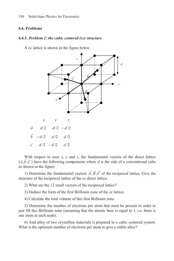
190 Solid-State Physics for Electronics
6.6. Problems
6.6.1. Problem 1: the cubic centered (cc) structure
A cc lattice is shown in the figure below.
/2 /2 /2
/2 /2 /2
/2 /2 /2
x y z
a d d d
b d d d
c d d d
With respect to axes x, y and z, the fundamental vectors of the direct lattice ( , ,a b c ) have the following components where d is the side of a conventional cube as shown in the figure:
1) Determine the fundamental vectors , ,A B C of the reciprocal lattice. Give the structure of the reciprocal lattice of the cc direct lattice.
2) What are the 12 small vectors of the reciprocal lattice?
3) Deduce the form of the first Brillouin zone of the cc lattice.
4) Calculate the total volume of this first Brillouin zone.
5) Determine the number of electrons per atom that must be present in order to just fill this Brillouin zone (assuming that the atomic base is equal to 1, i.e. there is one atom at each node).
6) And alloy of two crystalline materials is prepared in a cubic centered system. What is the optimum number of electrons per atom to give a stable alloy?
x
y
z
a
bc
d
Electronic Properties of Cu and Si 191
Answers
1) We can use for example 2 b cV
A , where 3
2( ) dV a b c is the volume
of a cubic cell. With b c that has components (d²/2, d²/2, 0), we thus obtain:
2 0 2
2 02
2 20
0
d d
A B Cd d
d d
These vectors exhibit the same components as the fundamental vectors of a face cc lattice for which each side of the cube is worth 4
d (rather than just d as is the
case in the direct lattice as shown in section 6.2.1). The up-shot is that the structure of the reciprocal lattice (of the cc direct lattice) is fcc.
2) The vectors of the reciprocal lattice are defined by:
, ,
2.
h k l
x y z
G hA kB lC
h l e h k e k l ed
The smallest vectors (G ) are vectors given by the following expressions, in which the signs vary independently from one another:
2x ye e
d,
2y ze e
d,
2x ze e
d.
3) The first Brillouin zone is delimited by the mediating planes of the preceding 12 G vectors. The vectors that join the origin to the centers of the faces of these zones are one-half of the preceding vectors:
x ye ed
, y ze ed
, x ze ed

192 Solid-State Physics for Electronics
We thus find ourselves with a regular dodecahedron. In an octant there are three faces given by AFC, BFC and AFB (see the figure). In all there are 3 × 8 = 24 faces, each sharing an adjacent octant so that there are in effect 12 faces throughout all space.
4) The volume in the first octant of the first Brillouin zone can be obtained as a
difference between the volume of the pyramid ABGCO and the pyramid FBGC. Thus, with:
2 3
ABGCO 31 2 2 83 3
Vd d d
and 2 3
FBGC 31 1 2 23 2 3
vd d d
we find the Brillouin zone volume in the first octant to be:
3 3 3
ZB1Oc 3 3 38 2 2
3 3V
d d d
from which the total volume of the Brillouin zone over all space is given by:
3
ZB1Oc 316
8V Vd
5) In a direct lattice with an atomic base equal to one atom per node, a cell with volume d3 contains on average two atoms per cell. The eight atoms situated at the eight corners of the cube are each shared between eight cells altogether bring one
F
A
B
C
kx
ky
kz
2, 0, 0
d
20, , 0
d
20, 0,
d
G
O

Electronic Properties of Cu and Si 193
atom per cell, and the atom at the center of the cell that is not shared with any other cell also brings one atom per cell, thus giving a total of two atoms per cell. If the volume of the material is equal to V, there are 3
V
d cells in direct space, so that there
are 23
V
dN atoms in the direct lattice.
In the reciprocal space, the volume of a cell is equal to 38
V. Therefore, in the
Brillouin zone we can place 3 3 216 8
33V
V dd= N cells. There are therefore in the
first Brillouin zone as many cells as atoms in the direct lattice, so all cells will be filled (with two electrons) if each atoms liberates two electrons. The Brillouin zone is thus totally filled if the atoms are divalent (a result identical to that found for a simple cubic or fcc lattice).
6) A stabilization of an alloy based on monovalent atoms (which by themselves can only fill half of the Brillouin zone) using divalent atoms is obtained when the equi-energy sphere tangential to the zone limit is filled with electrons. This means that the radius of this sphere is equal to:
1 22 2
2 2
OGR
d d
and that its volume is given by:
VF = 4
33
4 42 2
3 3R
d
The sphere thus contains 44 23 33 3
32 2 (8 ) 'd d
V V N cells whch is
equal to 2N ' electrons when filled. Under these conditions and with a population of
N atoms, we have 2N ' /N electrons per atom so that there are 2 23 33
2 V
d dV
23
1.48 electrons per atom.

194 Solid-State Physics for Electronics
6.6.2. Problem 2: state density in the silicon conduction band
To determine the form of the state density function for the silicon conduction band, we should note that in the neighborhood of mk (wave vector for a minimum in the conduction band where the minimum energy Emin = EC), we can write that the energy of a semi-free electron (of non-isotropic effective mass) is given by:
2 2 2* *
² ²
2 2C x m y z
tE E k k k k
m m
where:
*
2
²²
x
mE
k
and *
2 2
² ²² ²t
y z
mE E
k k
1) When introducing the vectors:
'*
'*
'*
*
*'
*t
t
x x
y y
z z
mk k
m
mk k k
m
mk k
m
and
' '*
' '
'
*
0
0
mx m m
m my
mz
mk k k
m
k k
k
what is the form of E = f(EC, 'k , 'mk ,m*)?
2) The reasoning used is with respect to k’ space, but what is the dimension of a primitive cell is this space? What is the equi-energy surface in this k’ space?
3) Determine the new expression for the state density function. What happens to this expression on taking into account the fact that the conduction band in reality displays six minima corresponding to six [100]-type directions that are equivalent and shown in Figure 6.3 (limited to the first octant and the equivalent directions [100], [010] and [001])?
4) Show how we are driven to defining a new effective mass (called the electron state density effective mass). How can it be expressed as a function of *m and *
tm ?

Electronic Properties of Cu and Si 195
Given that *00.90 m m and *
00.192 tm m (with m0 = 0.9 × 10⁻³⁰ kg), use the new expression for the effective mass as a function of m0.
Answers
1) We have ² ²* *2 2
2 2 2m mt
C x m y zE E k k k k , so that
– either *
*' m
mx xk k and *
*' ,m
mm mk k from which 2( )x mk k*
*' ' 2( ) .m
m x mk k
– or *
2 '2mtmy yk k and
*2 '2 ,mt
mz zk k in which case
* * *2' ' '2 '2* * *
2' ' '2 '2
² 1 1 12 * * *
²2 *
t tC x m y z
t t
C x m y z
m m mE E k k k k
m m mm m m
E k k k km
By introducing
'
'
'
'k x
k y
k z
k and '
00
'k m
mk , we finally reach:
2' '²
2 *C mE E k km
2) In reciprocal space, the dimension of a cell is 383
Vx y zk k k k (where V is the volume of the direct lattice). From:
*'*
*' ,*
*'*
mk kx x
m
mk ky y
mt
mk kz z
mt
196 Solid-State Physics for Electronics
we deduce that:
*'*
*' ,*
*'*
mk kx x
m
mk ky y
mt
mk kz z
mt
from which the dimension of a primitive cell in 'k space is:
3/ 23' ' '
* * 1/ 2* *
** * 8.x x x x x x
t t
mm mk k k k k k
Vm m m m
The relation obtained from question 1, i.e. ²2 *
2' '
mC mE E k k , makes it
possible to state that the equi-energy surface is a sphere centered at 'mk and with
radius given by 2 *'' .
m E ECmk k
3) In the k ' space, the volume corresponding to the energies between E and
(E + dE) is given by that between two spheres of radius '' mk k and
'' ' ,mk k dk in other words a volume 2'
' 4 ' '.k mdV k k dk From
2'' mk k 2 *,
²m E EC we deduce that 2 *
²'2 ' ' m dEmk k dk , and then that:
2'3
* 2 *' ' .C
mm m E E
k k dk dE

Electronic Properties of Cu and Si 197
In turn from this we have:
' 3
* 2 *4 C
km m E E
dV dE
The number of cells that can be placed in this volume is given by:
1/ 2* *'
' ' ' 3 3/ 23
1/ 2* *3
* 2 * 4
8 *
2 4
tCk
x y z
Ct
V m mm m E EdVdE
k k k m
E Em m V dE
h
Finally, relative to the unit volume of the material (V =1), we can place between the energy surfaces E and E + dE a number denoted Z(E) dE of electrons. This is given by (with two electrons per cell):
1/ 23/ 2 * *3
4( ) 2 t CZ E dE m m E E dE
h
Taking the six minima into account, the state density function can be written as:
1/ 23/ 2 * *3
4( ) 6 2 t CZ E m m E E
h
4) If 2/3* 1/ 2 *6[ ] ,c tm m m we have 4
31/ 23/ 2( ) 2 ,
hc CZ E m E E
which is an equation analogous to that obtained classically for 3D space. With *
00.90 m m and *00.192 tm m , we find mc = 1.05 m0.

This page intentionally left blank

Chapter 7
Strong Bonds in One Dimension
This chapter starts with a concise description of the origin and construction of atomic and molecular orbitals found in a covalent solid (molecular films and polymers included). The results are then applied to energy levels in 1D covalent materials (notably molecular wires).
7.1. Atomic and molecular orbitals
7.1.1. s- and p-type orbitals
In the approximation for an atomic configuration (that gives the quantum numbers n, l, m…), we assume that each electron of an atom moves in a potential that has a spherical symmetry. The result is that:
– the potential of the nucleus varies with respect to 1/r;
– this spherical potential gives a first approximation to the action of the other electrons.
The electronic state is thus represented by a wave function denoted n,l,m that is
dependent on three quantum numbers n, l and m, while the energy is only dependent on n and l (the degree of degeneration is equal to the number of values that m can take on). More details on this can be found in most basic courses on wave and atomic physics that use hydrogen as an example of a system with a spherical potential symmetry.

200 Solid-State Physics for Electronics
When l = 0, the atomic orbitals are denoted by the letter s and the wave functions only depend on n: n,l,m = R(r) ( ) ( ) = Rn,l l,m m = Rn,0 0,0 0, where:
0,0 02 1 and
2 2
These wave functions do not depend on nor ; only R(r) takes only different values as n, the principal quantum number, varies. The s-orbital thus has a spherical symmetry (as shown in Figure 7.1). The general expression for the radial functions
is given by 2 2
1 1 12 1
, ( ) expr r rna na na
ll
n l nl n lR r N L where L represents the
Laguerre polynomials and a1 is the first Bohr radius (0.53 Å). The fundamental state is written using 1/
0,1r aR Ce .
Figure 7.1. Representation of s orbitals
When l = 1, m = 1, 0, 1 and the orbitals are denoted by the letter p:
m = 0: 1,0 = ( 6 /2) cos and 0 = 1/ 2 m = 1: 1,1 = ( 3 /2) sin and 1 = (1/ ) cos
m = 1: 1,-1 = ( 3 /2) sin and -1 = (1/ ) sin
If R(r) represents the Rn,1 function, which does not change as m changes, the wave functions for the three preceding p states are of the form:
01 3 ( ) cos2
R r [7.1]
z z n = 1 n = 2 y y
x x
O O

Strong Bonds in One Dimension 201
11 3 ( ) sin cos2
R r [7.2]
11 3 ( ) sin in2
R r s [7.3]
with R(r) = R(rf) such that rf has a value defined by the relation:
2
0
( ) ² fr
R r r dr = 95%
(that indicates that the probability of the presence of an electron being inside the sphere of radius rf is equal to 95%), functions [7.1]–[7.3] give a conventional representation of the orbitals. NOTE.– The position of the M points are such that = OM, as shown in Figure 7.2.
We can use as a simple example the case where:
01 3 ( )cos2 2
R r = OM = OM.
Figure 7.2. The shape of the pz orbital. The + and – signs give the sign of 0 which is that of cos
z D M
pz orbital
O
x
y

202 Solid-State Physics for Electronics
Here D is the point on the Oz axis where = 1, and therefore we have:
1 3 ( )2
OD R r
In other words OM = OD cos . If [0, /2], we have OM > 0. The position of M points, as varies, is thus that of a sphere placed above the plane (xOy). If [ /2, ], cos 0, and the M points are placed like a symmetric sphere below the plane (xOy).
In addition, the signs of the 0, 1 1, orbitals can be obtained directly as a function of the signs taken on by the variables x, y and z. To do this, we use the correspondence between the spherical and Cartesian coordinates given (see Figure 7.3) by:
sin cos xr
sin sin yr
cos zr
(for example, if cos < 0, z < 0 and 0; see also Figure 7.2).
z M y
x m
Figure 7.3. Usually chosen spherical coordinates

Strong Bonds in One Dimension 203
With 1 ( )32
( ) R rr
f r > 0 (and r rf), the functions 0, 1 and 1 can thus
be written in the following way:
1 = X = x f(r) = px ( px > 0 or < 0 depending on whether x > 0 or x < 0)
1 = Y = y f(r) = py ( py > 0 or < 0 depending on whether y > 0 or y < 0)
0 = Z = z f(r) = pz ( pz > 0 or < 0 depending on whether z > 0 or z < 0)
Finally, the shape of the s- and p-orbitals can be schematically illustrated as in
Figure 7.4 (r is fixed to a value denoted rf which is such that 20
² ( )frr R r dr
95%). To conclude, we can state that the s-orbitals are non-directional, as opposed to
the p-orbitals that are.
Orbitals: ns npx npy npz nodal plane: (yOz) (xOz) (xOy) (nodal plane is where there is zero probability of presence)
Figure 7.4. Representations of ns and np atomic orbitals
NOTE.– The orbitals represented above are for one electron; these are the orbitals that will be used when building molecular orbitals when there is one electron that will be shared with a neighboring atom, as in a covalent bond. The atomic orbitals for an atom with i electrons are given by = i i where the i are wave functions for each i electron. The former are asymmetric (Pauli) and are placed under a Slater determinate form.
z
y
x
z
x
y
z
x
y
z
x
y

204 Solid-State Physics for Electronics
7.1.2. Molecular orbitals
7.1.2.1. Classic case of the H2+ molecular ion
A simple example is that of the first approximation where the overlap of adjacent orbitals is neglected (otherwise the supplementary condition E/ k = O should be used where there is a minimization of the energy according to a method of variation). With the two nuclei (protons) being situated at 1R and 2R and with the electron common to r (see Figure 7.5), the Hamiltonian of the system is (assuming that the nuclei are fixed in an adiabatic approximation):
0 1 0 2
² ² ² 2 4 4
e eH
m r R r R
If (r) = A exp( r/a1) is the wave function of the fundamental state of the hydrogen atom, this function is still a solution to the problem for (H2
+) if we assume that the electron is localized preferentially on one of the two nuclei:
– if the electron is localized about (1), (r) AD = 1r R = 1;
– if the electron is localized about (2), (r) BD = 2r R = 2.
If the electron is localized between the two nuclei, the solution must correspond
to a mixture of the two preceding states. This implies a search for a wave function for the molecular ion H2+ with a wave function in the form = c1 1 + c2 2. If the electron is localized at (1) then c1 1 and c2 = 0; if the electron is localized at (2), then c1 = 0 and c2 1.
eD (2) r (1) B 2R O 1R A
Figure 7.5. Layout of ions and electron in H2+

Strong Bonds in One Dimension 205
This function must satisfy the equation for proper values:
H | > = E | > so that H | c1 1 + c2 2 > = E |c1 1 + c2 2 >
On multiplying the left-hand side of the equation by < 1 | we obtain:
c1< 1 |H| 1 > + c2 < 1 |H| 2 > = E c1< 1 | 1 > + E c2 < 1 | 2 >
With the simplifying hypothesis which makes it possible to neglect the overlap integral S = < 1 | 2 > = 0, and with making H11 = < 1 |H| 1 > and H12 = < 1 |H|
2 >, we find that:
c1 H11 + c2 H12 = E c1
Similarly, multiplying the left-hand side with < 2 |, and with Hij = < i |H| j >, we have:
c1 H21 + c2 H22 = E c2
We thus obtain a system with two equations and two unknowns (c1 and c2), that can now be written as:
c1 (H11 – E) + c2 H12 = 0 [7.4]
c1 H21 + c2 (H22 – E) = 0 [7.5]
In addition,
– the wave functions 1 and 2 are real, thus making it possible to state that:
H12 = < 1 |H| 2 > = < 2 |H| 1 > = H21 = (with > 0);
– also, the problem (and hence the Hamiltonian) remains invariant with respect to any permutation of the nuclei A (index 1) and B (index 2), such that H11 = H22 =
(when > 0).

206 Solid-State Physics for Electronics
The preceding system of equations [7.4]. [7.5] with two unknowns finally yields a non-trivial solution when its determinate is zero. Using our notation, we have the equation ( + E)² ² = 0, which gives two solutions ( + E) = for energy that can be written as:
– EL = (the lowest energy corresponding to the bonding level as and are positive); and
– EA = + (the highest and therefore most unstable energy which corresponds to an anti-bonding level). (It can also be noted along the way that EA – EL = 2 .)
Placing EA into equations [7.4] and [7.5] gives us (c1 + c2) = 0, so that
c1 = c2 = cA. Similarly, by moving EL into [7.4] and [7.5], we obtain ( c1 + c2) = 0, so that c1 = c2 = cL.
The wave function for the H2
+ system thus accepts two solutions and they can be written as:
L = cL ( 1 + 2)
A = cA ( 1 2)
The normalization condition for the two functions L and A:
< L| L > = < A| A > = 1
makes it possible to determine that cL = cA = (1/ 2 ) and that:
1 21 ( )2L [7.6]
1 21 ( )2A [7.7]
We can thus go onto schematically represent these wave functions. Figure 7.6 shows the bonding solution where the electron has a high probability of presence between the two nuclei, so that the strong attraction between the electron and the nuclei bond the system. However, for the anti-bonding solution, the electron has a strong probability of presence on either outer side of the two nuclei such that the strong electrostatic repulsion between nuclei (1) and (2) destabilize the system.

Strong Bonds in One Dimension 207
NOTE.– With S = < 1 | 2 > 0 (overlap integral), the same but longer calculation gives:
1 2
1 2
12(1 )
12(1 )
L L
A A
ESS
ESS
[7.8]
Figure 7.6. Wave functions and orbitals for H2+
(bonding state on the left and anti-bonding state on the left)
7.1.2.2. The H2 molecule
In this system, there are two electrons and they are assumed to be at the same potential as the electron in the H2
+ system. This is because to a first approximation it is possible to assume that the interaction potential between the two electrons is negligible.
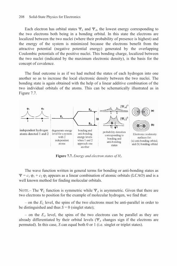
208 Solid-State Physics for Electronics
Each electron has orbital states L and A, the lowest energy corresponding to the two electrons both being in a bonding orbital. In this state the electrons are localized between the two nuclei (where their probability of presence is highest) and the energy of the system is minimized because the electrons benefit from the attractive potential (negative potential energy) generated by the overlapping Coulombic potentials of the positive nuclei. This bonding charge, localized between the two nuclei (indicated by the maximum electronic density), is the basis for the concept of covalence.
The final outcome is as if we had melted the states of each hydrogen into one
another so as to increase the local electronic density between the two nuclei. The bonding state is again obtained with the help of a linear additive combination of the two individual orbitals of the atoms. This can be schematically illustrated as in Figure 7.7.
Figure 7.7. Energy and electron states of H2
The wave function written in general terms for bonding or anti-bonding states as = c1 1 + c2 2 appears as a linear combination of atomic orbitals (LCAO) and is a
well known method for finding molecular orbitals.
NOTE.– The L function is symmetric while A is asymmetric. Given that there are two electrons to position for the example of molecular hydrogen, we find that:
– on the EL level, the spins of the two electrons must be anti-parallel in order to be distinguished and thus S = 0 (singlet state);
– on the EA level, the spins of the two electrons can be parallel as they are already differentiated by their orbital levels ( A changes sign if the electrons are permuted). In this case, S can equal both 0 or 1 (i.e. singlet or triplet states).

Strong Bonds in One Dimension 209
7.1.3. - and -bonds
7.1.3.1. -bonds
These are molecular orbitals which have a symmetry about an axis drawn between the two atoms that are covalently bonded. From s-orbitals (the fundamental state for hydrogen) we have as an example the structure shown in Figure 7.8.
Figure 7.8. 1s and * 1 s-orbitals
If the axis (Ox) is that on which the two atoms A and B are placed then the 2px orbitals will have an appearance much like that shown in Figure 7.9.
Figure 7.9. 2p and * 2p orbitals
where:
12 2 2( )
x xL A p B p and 12 2 2( )
x xA A p B p .
7.1.3.2. -bonds
These are molecular orbitals that take on a plane of symmetry than goes through the line Ox that joins the atoms and is perpendicular to the direction Oy for 2pz orbitals or perpendicular to the direction Oz for 2py orbitals.
+ *u
g
C

210 Solid-State Physics for Electronics
Figure 7.10. 2pz , * 2pz , 2py , and * 2py orbitals
NOTE.– The molecular orbitals are termed paired (and denoted g for “gerade” from the German) and when following a symmetric operation around the center (C) of symmetry of the molecule the sign of the orbital does not change. When the sign does change, the orbitals are denoted by with the letter u to indicate “ungerade”. So, bonding -orbitals are paired and denoted g, while anti-bonding orbitals * are unpaired and denoted *u. Bonding -orbitals are unpaired and denoted u, while anti-bonding *-orbitals are denoted *g.
7.1.4. Conclusion
Following the introduction of the principal types of atomic and molecular orbitals (bonding across two atoms) we will now look at an assembly of bonds in a linear atomic chain (1D solid).
7.2. Form of the wave function in strong bonds: Floquet’s theorem
7.2.1. Form of the resulting potential
An infinite chain of atoms each spaced a distance a apart (thus a is the lattice period) is shown in Figure 7.11. The distance a is such that a 2R where R is defined in the figure. The atoms in the chain are numbered …(0), (1), (2), …(s–1), (s),…, so that by placing the atom denoted (0) at the origin, any atom called s has a distance from the origin given by rs = sa.
O+
+
u
*g C

Strong Bonds in One Dimension 211
(0) (s) (s - 1)(2)(1)
asrs
a
'r 'rr
ar ra)2s(r
asr
a)1s(r 1s 1srr
Figure 7.11. Layout of atoms in an infinite 1D chain
So within this geometric system, the potential generated by an atom (s) at a point in space located by r , such that vs( r ), is the same as that generated by an atom (0) at a point 'r and similarly denoted v0( 'r ). By making sr sa , and on remarking that r s + 'r = r , we finally have vs( r ) = v0( 'r ) = v0( r - r s).
Outside of the action of an atom (s), an electron placed at r will be subject to
the action of neighboring atoms, with the atom (s – 1) generating at r the potential vs-1( r ) = v0( 1sr r ), and so on.
The resulting potential at r can thus be defined for a chain of infinite length by:
V( r ) = 0( ) ( )s s
s ss s
v r v r r [7.9]
Now we can state that the resultant potential V( r ) is periodic with a period of a , as the symmetry of the problem of an infinite chain demands that the resultant potential at r is the same as that calculated at r a , …, r sa , and so on whether the whole number s be negative or positive. This means that:
V( r ) = V( r a ) = V( r sa ) [7.10]
Each electron is dropped into a potential V( r ) that displays a periodic function, and therefore the wave function is a Bloch function. This result will be used in section 7.2.3 to establish Floquet’s theorem.

212 Solid-State Physics for Electronics
7.2.2. Form of the wave function
e-(s –1) (s) (s +1)
a
Figure 7.12. A system of practically independent atoms
If the atoms are well spaced out from one another, as in Figure 7.12, the valence electron attached to each nucleus s is not affected by the nucleus’s neighbors. And in this case the potential discerned by an electron placed at r can be reduced to:
vs( r ) = v0 sr r
and thus we have V ( )r v0 sr r . Similarly, the wave function for the electron is that obtained for a single atom s,
that is an atomic wave function [ s( r )]. If the atoms are brought closer to one another, then neighbors will start to
provoke effects on the electron placed at r , and the form of the wave function will resemble that given for a molecular orbital by the LCAO method (see section 7.1.2), as in:
( ) ( )s ss
r c r [7.11]
where ( )s r is the wave function of an electron placed at r and belonging to an atom denoted s.
We can see that the form of equation [7.11] resembles that of [7.9] for the
potential followed by the electron.

Strong Bonds in One Dimension 213
Using an argument similar to that applied to the potential makes it possible to state that the wave function ( )s r for the electron placed at r belonging to the atom s is identical to that of the same electron placed at 'r on the atom 0, so that:
( )s r = 0 ( ')r , and then with 'sr r r , ( )s r = 0 ( )sr r
As a definition, and by analogy to the potential described in equation [7.9], we can write that:
0( ) ( )s ss
r c r r [7.12]
7.2.3. Effect of potential periodicity on the form of the wave function and Floquet’s theorem
We can now state that the wave function for an electron placed at r and belonging to an infinitely long chain can be written:
– either in the form of a linear combination from equation [7.12]:
( )r 0 ( )s ss
c r r , this being a Hückel development of the wave function;
– or in the form of a Bloch function, with the potential to which the electron is submitted being periodic so that (see Chapter 3):
( ) ( )ikrk r e u r , where ( ) ( )u r u r a [7.13]
The Bloch form applied to a wave function calculated for r a makes it possible to state that:
ik(r a) ika ika( ) ( ) ( ) ( )ikrk kr a e u r a e e u r e r [7.14]
and, by developing ( )k r as found in equation [7.14] and according to Hückel from equation [7.12], we find an initial expression for ( )k r a :

214 Solid-State Physics for Electronics
0 0 1 0
0
( ) [... ( ) ( ) ... ( ) ...]
ikak
s
r a e c r c r ac r sa
[7.15]
However, the Hückel development directly carried out on ( )k r a gives:
0 0 1 0
0 s 1 0
( ) ... ( ) ( ) ... ( ) ( [ 1] ) ...
k
s
r a c r a c r a ac r a sa c r a s a
[7.16]
The identification, term by term, between equation [7.15] and [7.16] gives, for example:
0 0 1 0( ) ( )ikae c r c r , so that .1 0= .ik ac c e
1 0 2 0 ( ) ( 2 )]ikae c r a c r a a , so that 2 1= ikac c e
0 ( )]ikase c r sa 1 0 ( [ 1] ),sc r a s a so that 1= ika
s sc c e
In general terms we thus have:
21 2 0 0= = = ... = = .sik rika ik a ik sa
s s sc c e c e c e c e [7.17]
With this we are brought to the final form of the wave function (Floquet’s theorem) that can be written in two equivalent forms (using the notation
( ) ( )kr r ):
0
0
( ) ( ) so that with
( ) ( ) ( ),
s
s
ik rs s s
s
ik rk s
s
r c r c c e
r r c e r [7.18]
or rather:
.0 0 0( ) ( ) ( ) with =sik r
k s s s ss s
r c r r c e r r r sa [7.19]
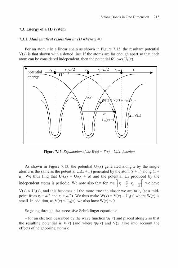
Strong Bonds in One Dimension 215
7.3. Energy of a 1D system
7.3.1. Mathematical resolution in 1D where x r
For an atom s in a linear chain as shown in Figure 7.13, the resultant potential V(x) is that shown with a dotted line. If the atoms are far enough apart so that each atom can be considered independent, then the potential follows U0(x).
Figure 7.13. Explanation of the W(x) = V(x) – U0(x) function
As shown in Figure 7.13, the potential U0(x) generated along x by the single atom s is the same as the potential U0(x + a) generated by the atom (s + 1) along (x + a). We thus find that U0(x) = U0(x + a) and the potential U0 produced by the independent atoms is periodic. We note also that for
2 2 , a a
s sx r r we have
V(x) U0(x), and this becomes all the more true the closer we are to rs (at a mid-point from rs a/2 and rs + a/2). We thus make W(x) = V(x) – U0(x) where W(x) is small. In addition, as V(x) < U0(x), we also have W(x) < 0.
So going through the successive Schrödinger equations:
– for an electron described by the wave function k(x) and placed along x so that the resulting potential is V(x) (and where k(x) and V(x) take into account the effects of neighboring atoms):
rs – 1 rs-a/2 rs rs+a/2 rs + 1 x
O’
U0(x)
V(x)
W(x) = V(x) – U0(x)
a U0(x+a)
potential energy

216 Solid-State Physics for Electronics
²( ) ( ) V( ) ( )2k k kE x x x x
m [7.20]
– for an electron positioned with respect to x and belonging to an isolated atom numbered s, its wave function is s(x) = 0(x – sa), while the potential is U0(x) = U0(x – sa). Denoting its energy with E0, we have:
0 0 0 0 0²( ) ( ) U ( ) ( )
2E x sa x sa x x sa
m [7.21]
Multiplying the two sides of this equation by c0 sikre (where rs = sa) and summing over s:
0 0 0 0 0
0 0
²( ) ( )2
( ) ( ).
s s
s
ikr ikrs s
s sikr
ss
E c e x r c e x rm
U x e x r
This equation can be rewritten with equation [7.19] in mind:
0 0²( ) ( ) U ( ) ( )
2k k kE x x x xm
[7.22]
Taking the difference between equations [7.20] and [7.22], we have:
(E – E0) k(x) = [V(x) – U0(x)] k(x) [7.23]
With the potential V(x) being periodic, we have V(x) = V(x – rs), such that:
W(x) = [V(x) – U0(x)] = [V(x – rs) – U0(x – rs)] = W(x – rs) [7.24]
Note that W(x – rs) is a periodic function of a, and as such is independent of s. This parameter can therefore be included or omitted from .
s

Strong Bonds in One Dimension 217
Finally, equation [7.23] gives, by developing k(x) according to Floquet, as in equation [7.19],
(E – E0) k(x) = c0 0( ) ( )sikrs s
s
e W x r x r [7.25]
7.3.2. Calculation by integration of energy for a chain of N atoms
Multiplying equation [7.25] by k*(x) and integrating over all N atoms numbered from 0 to (N – 1) directly gives:
0
0 0
( ) ( )
c ( ) W( ) ( ) .s
k k
ikrk s s
s
E E x x
e x x r x r dx [7.26]
With the help of equation [7.19], the calculation of ( ) ( )k kx x that appears in equation [7.26] can be performed:
1 12 ( )
0 0 s 0 t0 0
( ) ( ) ( r ) ( r )s N t N
i ks kt ak k
s t
x x c e x x
As 0 0( ) ( )s tx r x r = ts (with t
s = 1 if s = t; ts = 0 if s t), we have:
1 12 ( )
00 0
12 2( )
0 00
( ) ( )
.
s N t Ni ks kt a t
k k ss ts N
i ks ks a
s
x x c e
c e c N
The normalization condition of the function k(x), < k(x)| k(x)> = 1 = |c0|² N, makes it possible to obtain:
01
cN
[7.27]

218 Solid-State Physics for Electronics
Equation [7.26] makes it possible to deduce (with equation [7.19]):
k*(x) = c0* 0( )tikr
tt
e x r
(E – E0) 2
0 0 0 ( ) W( ) ( )s tikr ikrt s s
s t
c e e x r x r x r dx
so that with equation [7.27],
E – E0 ( )0 0
,
1 ( ) W( ) ( )ik s t a
s t
e x ta x sa x sa dxN
This expression can also be written as:
E = E0 ( )0 0
,
1 ( ) W( ) ( )ik s t a
s t
e x ta x sa x saN
[7.28]
Using the Hückel conditions, which only retain couplings between first neighbors:
0 0( ) ( ) ( )
when (with > 0 as < 0) ( ) ( ) when 1
0 for other cases.t s
x ta W x sa x sa
s t Wx W x s t
[7.29]
(as W < 0, then > 0 if the orbitals t and s have the same sign). In this approximation, expression [7.28] for energy following the sum over s (that varies from s0 = 0 to sN-1 = N –1) gives
00
11
11
( )0
( )
( )
1
NN
ik s t at s
tik s t a
t st
ik s t at s
t
E E e WN
e W
e W
[7.30]

Strong Bonds in One Dimension 219
Each term of the sum between the brackets that carries N terms (as s has N values) in fact gives the same contribution, with each being of the form:
( ) j
j
ik s t at s
t
e W
= eik(0) a ( ) + eik( 1) a ( ) + eik(+1 ) a ( ) = e ika eika
sj = t sj = t – 1 sj = t + 1
Finally the bracket of equation [7.30] is equal to N [ e ika eika], and the energy (E) for the expression is now:
E = E0 e ika eika = E0 22
ika ikae e
= E0 – [ + 2 cos ka],
which can be rewritten:
E = E0 – 2 cos ka [7.31]
The graphical representation of E = f(k) (energy dispersion curve) is given in Figure 7.14. It shows that the amplitude of the variation in E as a function of k amounts to 4 ; the permitted bands are as wide as are large (strong transfer integral between electrons on closest neighbors).
Figure 7.14. The dispersion curve E = f(k) from strong bond and Hückel approximations
E E0 - + 2 E0 - - 2 - /a - /2a 0 /2a
/
k
4
E0 E0

220 Solid-State Physics for Electronics
7.3.3. Note 1: physical significance in terms of (E0 – ) and
From equation [7.21],
²20 0 0 0 0( ) ( ) U ( ) ( )
mE x sa x sa x x sa ,
and equations [7.29]:
0 0 0 0²( ) U ( ) ( )
2E x sa x x sa
m [7.32]
0 0( ) W( ) ( )x sa x sa x sa (one of the Hückel conditions [7.29])
so that with W(x – sa) = W(x) (period of W: equation [7.24]):
E0 = 0 0 0²( ) U ( ) W( ) ( )
2x sa x x x sa
m
= 0 ²( ) U ( ) W( ) ( )
2s sx x x xm
so that:
(E0 - ) = ²( ) (x) ( )2s sx V x
m [7.33]
as V(x) = U0(x) + W(x). The bracketed terms indicate that:
– the E0 term represents the energy of an electron situated on a given atom s within a potential generated only by that atom (potential is U0(x) as detailed in equation [7.32]);
– the ( ) term represents the energy of an electron (on a given atom s) influenced by atoms that are neighbors to the principal atom (potential is W(x) as given in equation [7.29]);
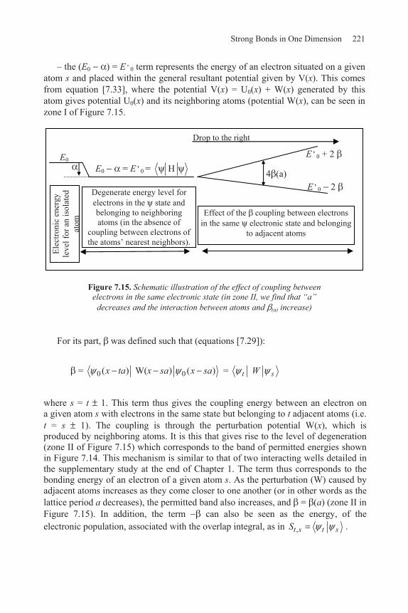
Strong Bonds in One Dimension 221
– the (E0 ) = E ' 0 term represents the energy of an electron situated on a given atom s and placed within the general resultant potential given by V(x). This comes from equation [7.33], where the potential V(x) = U0(x) + W(x) generated by this atom gives potential U0(x) and its neighboring atoms (potential W(x), can be seen in zone I of Figure 7.15.
Figure 7.15. Schematic illustration of the effect of coupling between electrons in the same electronic state (in zone II, we find that “a”
decreases and the interaction between atoms and (a) increase)
For its part, was defined such that (equations [7.29]):
= 0 0( ) W( ) ( )x ta x sa x sa = t sW
where s = t 1. This term thus gives the coupling energy between an electron on a given atom s with electrons in the same state but belonging to t adjacent atoms (i.e. t = s 1). The coupling is through the perturbation potential W(x), which is produced by neighboring atoms. It is this that gives rise to the level of degeneration (zone II of Figure 7.15) which corresponds to the band of permitted energies shown in Figure 7.14. This mechanism is similar to that of two interacting wells detailed in the supplementary study at the end of Chapter 1. The term thus corresponds to the bonding energy of an electron of a given atom s. As the perturbation (W) caused by adjacent atoms increases as they come closer to one another (or in other words as the lattice period a decreases), the permitted band also increases, and = (a) (zone II in Figure 7.15). In addition, the term can also be seen as the energy, of the electronic population, associated with the overlap integral, as in ,t s t sS .
(I) (II)
Degenerate energy level for electrons in the state and belonging to neighboring atoms (in the absence of
coupling between electrons of the atoms’ nearest neighbors).
Effect of the coupling between electrons in the same electronic state and belonging
to adjacent atoms
4 (a)
Drop to the right
E0 = E ' 0 = H E ' 0 + 2
E ' 0 2
E0
Elec
troni
c en
ergy
le
vel f
or a
n is
olat
ed
atom

222 Solid-State Physics for Electronics
7.3.4. Note 2: simplified calculation of the energy
With ²2
( )m
H V x , according to equation [7.32] we have:
(E0 ) = E ' 0 = ( ) ( )s sx H x
Often, the term (E0 ) = E ' 0 is simply denoted by as it can be obtained through a more direct and simple route (that has the inconvenience of hiding several physical realities).
In effect, it is possible to state directly that:
( )
( )( )
ik s t as t
k k s tik s t a
k k s ts t
e HH
E E ke
.
Using the fact that s t = st and noting that the Hückel approximations can be given by:
– Hss = s sH = = Coulomb integral = a negative constant by taking the origin of the energies as those of an electron at infinity;
– Hst = s tH = when s t and s and t are adjacent ( < 0, is the resonance integral, also called the transfer integral, between electron s and electron t).
It is possible to directly obtain (as the number of upper and lower terms are
identical as the sum making it possible to avoid the tortuous double sum):
E = E(k) = eika e ika = 2 cos (k · a).

Strong Bonds in One Dimension 223
It should be noted that in this version of the Hückel approximation:
– on one hand, the term Hss = is identical to that of E ' 0 = E0 from section 7.2.2; and
– on the other hand, the term Hst = when s = t 1, can be written as:
Hst = s tH = ²- ( )2s tV x
m
= 0² ( ) ( )
2s tU x W xm
= E0 s t + s tW = .s tW
and the value of is that proposed at the start of section 7.2.2.
7.3.5. Note 3: conditions for the appearance of permitted and forbidden bands
So that a forbidden band appears (zone II in Figure 7.16), the rupture of the bands must come from two or more distinct levels (zone I in Figure 7.16). This can give the system summed in Figure 7.16, where there is a chain of atoms of which each has two distinct states given by and and such that 0' |E H and
0' |E H . The gap EG can therefore appear in a crystal made up of atoms
that incorporate various different types of electrons (for example s and p), in a crystal made up of different type of atoms (see section 7.4.1), and indeed in a crystal with an asymmetric cell (see section 7.4.2).
In zone II of Figure 7.16, where the atoms are brought together, each degenerate
level breaks down to permitted bands, with each of these at least initially being related to the starting state. When the rupture is sufficiently large, i.e. when a is small enough, for the states to mix, then the two permitted bands are separated by a forbidden band, this being at the point M in the figure. Figure 8.10, for carbon, shows this state of affairs more closely for 3D.

224 Solid-State Physics for Electronics
Figure 7.16. A first approximation to the appearance of the forbidden band taking into account the electrons in the two states denoted for of each atom
7.4. 1D and distorted AB crystals
7.4.1. AB crystal
A 1D crystal made up of an alternating distribution of A and B type atoms (Figure 7.17 with in all 2n = N atoms) has N/2 A–B atom pairs.
Figure 7.17. Alternating chain of n pairs of A and B atoms, where n varies from 1 to N/2
It is possible to see straight away that the primitive cell (which encloses one whole AB unit) has a period of 2a. EA and EB denote the energy levels of electrons situated on atom A and atom B, respectively, and A and B are the corresponding wave functions.
0'E + 2
0'E = H (permitted band)
0'E – 2 M
0'E + 2
0'E = H 0'E 2 (permitted band)
Two degenerate energy levels corresponding to the two states, and
, of each atom. Adjacent atoms are electronically independent (no
electronic coupling).
Coupling effect between adjacent atoms each with two, different electronic states, and (where for example,
= t sW ).
EG Forbidden band
Atoms move closer, i.e. a decreases
(I) (II)
A1 B1 A2 B2 Aj Bj An-1 Bn-1 An Bn
a a

Strong Bonds in One Dimension 225
The problem can be put into two equations similar to that of equation [7.20]. One equation relates to each atom, A or B. The states in themselves can then be sought through a linear combination of atomic orbitals for a chain of N/2 A and B atoms, as in:
N/2
kjj 1
k Aj kj Bj
with, according to Floquet’s theorem, 2ikj akj ka e and 2ikj a
kj kb e . Once again using assuming poor overlap between adjacent neighbors, we have:
Ai Aj ij Bi Bj and 0Ai Bj
and the wave function, following normalization using 2 2 1k ka b , is:
/21/2
1exp 2
N
k k Aj k Bjj
N ikj a a b
The equation for proper values is k k kH E , with:
²2 Aj Bj
j j
H V Vm
and the VAj and VBj potentials are defined as for a single type of atom.
Successive multiplication of the equation for proper values by Aj and then by
Bj gives rise to two types of equations with a compatibility that is given by

226 Solid-State Physics for Electronics
a second-order equation carrying the coefficients A and B of the form A A B AV and B B A BV .
The upshot is that there are two solutions for the energy. The separation between
them, E = E+min E max, is equal to the forbidden band. This conclusion is shown
schematically in Figure 7.18. When k = 0, the state with the lowest energy belongs to the curve denoted E . It is represented by a bonding orbital, here called L. Still with k = 0, the state with the highest energy is found in the curve E+ and is represented by an anti-bonding orbital, here denoted by A.
Figure 7.18. Dispersion curve, E = f(k), for the AB diatomic system of period 2a
7.4.2. Distorted chain
7.4.2.1. Representation
a a u u u= a1/2 u=a1/2 A1 A’1 A2 A’2 Aj Aj a + a1 a-a1 2a distorted chain
undistorted chain
Figure 7.19. Distorted AA’ chain, where the atoms A and A’ are identical but separated by bonds of alternating lengths
E
k /2a + /2a
E+min=EB 2 B
E max = EA 2 A
E+
E
A state
L state
E
Reduction to the first zone, i.e. an interval between [ /2a, + /2a] for
a crystal of period equal
to 2a.
a
a

Strong Bonds in One Dimension 227
If each atom (A) is displaced by a distance given by u = 12a
with respect to its
initial rest position in a chain with period a, then the result is the structure shown in Figure 7.19. The period is now equal to 2a (as in section 7.4.1), but now there is only one type of atom, i.e. A ' ), and hence EA = EA’.
The upshot is the band scheme shown in Figure 7.20. The E(k) curve for the
undistorted chain (with a period equal to a) is traced by the dashed line, while that for the distorted crystal (with a period of 2a) is drawn as a full line. The distortion gives rise to a gap (EG) that changes with k = /2a.
Figure 7.20. E = f(k) dispersion curves for distorted (continuous line) and undistorted
dashed line) crystals. Making '1 HA Aj j = - 1 and 'HA Aj j = - 2 , we have:
E(k = /2a) = EG = 2 ( 1 - 2). In addition, supposing that 1 and 2 are of the form - 1 = - + u and - 2 = - - u (where > 0), calculation gives EG 4 |u|.
7.4.2.2. Conditions to generate a distorted chain
Whether or not a distorted chain will arise is governed by the energy required to produce a chain deformation (bond alternation) and the electronic energy gained through relaxation, respectively denoted Edefor and Erelax, following the opening of a gap:
– Edefor is the energetic cost of going from a chain of period a to a structure of period 2a, which alternates “long” and “short” bonds, as in (a + a1) – short bond (a a1). It can be stated as Edefor = 1
22 ²eNk u = 2keNu² , where N is the number of
atoms of type A or A ' , |2u| is the stretching or contraction modulus of the spring that mechanically ties two adjacent atoms. This brings in the harmonic coupling of atoms
EG Erelax
E
k /a /a /2a + /2a
E+
E
E
EA - 2 ’A
EA 2 A O
Reduced to the first zone [- /2a, + /2a] for a distorted crystal of period 2a

228 Solid-State Physics for Electronics
through an elastic force (fe) with a constant (ke) where fe = - ke (2u). If 2u > 0, fe < 0 and is a force of attraction.
– The electronic relaxation energy (Erelax) is the drop in energy of the system in going from the filling with electrons of the system with period a to the filling of the system based on the period 2a. See Figure 7.20, where Erelax is only an approximate value corresponding to the drop in energy of electrons that may participate in the conduction of the most energetic electrons. See the notes in section 7.5.3 for a more rigorous treatment.
If E = Edefor - Erelax < 0, that is to say that the gain in energy during the
relaxation is greater than that of the deformation, then there is a drop in the system’s energy. This stabilizes to a point of deformation with a value (u0) such that
0
0.Eu u u
So, the dimerization of the system, that is the generation of
alternating short and long bonds, leads to an opening in the gap that changes with k = /2a. This is the so-called Peierls transition, which corresponds to a metal–insulator transition.
7.5. State density function and applications: the Peierls metal-insulator transition
7.5.1. Determination of the state density functions
First, a quick recall of the evaluation of the n(k) function (see also Chapters 2 and 5). In reciprocal space, the electrons are spread throughout cells of size
2.
Lk This cell dimension is the quantification of the k space and is obtained
through the progressive boundary condition (PBC, or Born-von Karman conditions). At the interval 2
,L
k it corresponds to an average of the electronic function
denoted ( )k x , which in turn can give two states if spin is taken into account. This
also makes it possible to obtain, for the same k state, the two functions ( )k x and
( )k x . It is therefore possible to state that:
n(k). k = n(k).1
2
LL= 2 n(k) = 1

Strong Bonds in One Dimension 229
The energy state density function [Z(E)] is now related to n(k) by Z(E) dE = 2 n(k)dk, from which we deduce that:
Z(E) = 2 1dEdk
Using this with a chain of N atoms, we have equation [7.31], where E = E0 – 2 cos ka, and then as 2 sin dE
dka ka , it is possible to state that
1 1( )sin
Z Ea ka
With:
sin²(ka) = 1 – cos²(ka) = 1 2
0 2
E E
we obtain:
20
1 1( )
12
Z Ea E E
For a chain of length (L) given by L = Na, the number of states is:
N(E) Na Z(E) 0
2
2
1
1 E E
N
2 2
0
2 1 .(2 ) ( )
N
E E
The graphical representation is given in Figure 7.21b.

230 Solid-State Physics for Electronics
Figure 7.21. (a) E = f(k) dispersion curve; and (b) state density curve for a chain of N atoms
7.5.2. Zone filling and the Peierls metal–insulator transition
7.5.2.1. Filling an undistorted zone
For an undistorted chain with N atoms (length equal to Na) and N electrons (one electron per atom in a single quantum state), the number of primitive cells of dimensions 2 /L = 2 /Na that can be placed in a Brillouin zone of size 2 /a (placed between k = - /a and k = /a) is given by:
2
2a
Na
N
As spin makes it possible to place two electrons into each primitive cell, we can place, altogether, 2N electrons into the zone. Given that the system only liberates N electrons, this zone (also described by the dashed line in Figure 7.20) is only half full. The electrons can therefore easily move about as there are numerous available places, and the system is metallic.
7.5.2.2. The metal–insulator transition
When the distortion is energetically favored, as in the distorted crystal discussed in section 7.4.2 that gave the continuous line for E = f(k) in Figure 7.20, the zone has the dimension /a (as it is only between k = – /2a and k = /2a), and only N/2 cells can be placed, that is only N electrons. The zone is totally filled by the system’s N electrons, which can no longer move (now placed on the inside of the E = f(k) line
- /a - /2a 0 /2a /a
k
4
E0 E0
E0 - + 2
E0 - - 2
E
k = 2 /L
E
EF
N(E)
=Z(E).L N/
(b) (a)
EF
kF

Strong Bonds in One Dimension 231
shown in Figure 7.20). A transition from a metallic to an insulating state has occurred; in other words the system has undergone a Peierls transition.
7.5.2.3. Wave vector at the Fermi level: the position of EF
For a linear chain of N atoms, each liberating a single electron from the state under consideration, that has a period a and hence length L = Na, we can evaluate the wave vector (kF) at absolute zero for electrons that have the highest energy, i.e. the Fermi energy which separates the occupied states from the empty states at T = 0 K. At absolute zero, the temperature at which the Fermi-Dirac distribution function F(E) = 1 when E < EF (and F(E) = 0 when E > EF), the number of N electrons in the chain of length L can be calculated with the help of the state density functions Z(E) or n(k) and must be such that:
N =
min
( ) ( )E
F E N E dE =
min
( )FE
E
N E dE =
min
. ( )FE
E
L Z E dE
N = ( ) ( )N k F k dk = ( )F
F
k
k
N k dk
=F F
F F
F1( ) (2 )
k k
k k
NaL n k dk Na dk k
from which:
F 2k
a
where N(E) is the state density for the chain of length L. We can thus see in Figure 7.21 that for an undistorted chain, the energy EF that corresponds to
2aFk is such that EF
= E0 . For a distorted chain, that contains N atoms liberating N electrons, we again have
2.
aFk The Fermi level, at 0K situated midway between the occupied and
empty levels, is in the middle of the gap EG shown in Figure 7.20.

232 Solid-State Physics for Electronics
7.5.3. Principle of the calculation of Erelax (for a distorted chain)
Section 7.4.2.2 detailed how the relaxation energy is the difference between the energy of electrons belonging to an undistorted chain (End) and those same electrons in a distorted chain, i.e. Erelax = End Ed.
The estimation of Erelax shown in Figure 7.20 uses the knowledge that:
– for the undistorted chain, (dashed line for E = f(k)), the electrons participating in the conduction are the most energetic and hence situated at EF. As we have just seen, this energy varies with k =
2aFk , and as shown in the figure, corresponds
to the energy EF at the intersection of the energy and 0K axes;
– for the distorted chain, the zone between 2a
and 2a
is just filled, so that the
most energetic electrons, which participate in transport, are at the summit of the band denoted E , that is at EA 2 A.
The energy Erelax shown in Figure 7.20 thus corresponds to the difference in energy of the transport electrons in the undistorted and distorted (or so-called dimerized in chemistry) chains.
A more rigorous estimation of Erelax= End Ed can now be carried out knowing that in both cases (calculating End and Ed) the electrons fill cells between –kF and +kF in the k space.
We thus have:
End = ( ) ( )F
F
k
k
E k N k dk =/2
/2
( ) ,a
a
LE k dk with E(k) = E0 – – 2 cos ka
(E(k) for the undistorted chain).
Similarly, the energy (Ed) of the distorted system is given by Ed = /2
/2( ) ,La
aE k dk where E (k) is the energy function of the distorted system traced
in Figure 7.20. The resulting calculations are rather long, and can be carried out as an exercise!

Strong Bonds in One Dimension 233
7.6. Practical example of a periodic atomic chain: concrete calculations of wave functions, energy levels, state density functions and band filling
This section looks at the electronic properties of a 1D (along x) atomic chain of length L and made up of N atoms regularly spaced apart by a periodic distance called a, so that L = Na. A concrete treatment will be made of a closed, cyclic chain using N = 8.
7.6.1. Range of variation in k
The range is obtained from the progressive boundary conditions (PBC, or Born-von Karman conditions). As we have seen, these conditions indicate that when the chain is turned back on itself, the presence probability for an electron at a certain x coordinate is unique and does not depend on the number of turns (of length L) carried out by the electron on the chain and hence ( ) ( ).x x L
The PBC conditions applied to the Bloch function (section 5.8.2.1.1) yield
eikL = 1. As in general terms, 1 = ei2p (with p being whole) and here with L = Na, we can
deduce that:
2pp
k kNa
(where p is a positive or negative integer or zero, as in p = 0, 1, 2, 3,…).
In addition, the energy is given by equation [7.31], so that:
E = E0 – 2 cos ka = E0 – 2 cos kpa
8 0 1 7 2 6 3 5 4
Figure 7.22. A cyclic “linear” chain with N = 8

234 Solid-State Physics for Electronics
With the E(k) curve being periodic, we can limit the representation to one period (all other periods will give the same solution for energy). This gives E(k) over a reduced zone that extends from – ka , and such that with k = kp we have:
pka a
(reduction to the first Brillouin zone). As 2 pNapk , we also have
2 N
,2Np so that p takes on N successive values.
7.6.2. Representation of energy and state density function for N = 8
As we have seen, the domain in which 2 pNapk varies can be reduced to:
pka a
When N = 8, and 4pk pa
, the successive values of kp (where 2 2N Np ,
so that p 4, 3,..0,...3, 4 ) are therefore:
kp = 3 3, , , , 0, , , , .4 2 4 4 2 4a a a a a a a a
Equation [7.31] for energy can thus be written as:
E = E0 – - 2 cos pk a = E0 – - 2 cos4
p
E = f(kp) and Z(E) are represented in Figures 2.23a and b.

Strong Bonds in One Dimension 235
Figure 7.23. (a) E = f(kp); (b) Z(E); and (c) the number of states, all for N = 8
With respect to 4 ak and 4 a
k the states are shared with adjacent zones,
such that only one of these states is compatible. It should be mentioned that the states at the top (k–3 , k3 and k4) and the bottom
(k–1, k1 and k0) of the band are “squashed” and in contrast to those at the middle (k–2 and k2) of the band. This arises from the cosine shape of the energy curve that is flattened towards the top and bottom, and more vertically inclined near the middle. This effect increases with N, but to show this in Figure 7.23 would end up with an overload! This is because as N increases and along with it the number of values that kp takes on, the energy levels will become extremely close to one another at the bottom and top of the band. Qualitatively, this explains the shape of Z(E). In addition, this function gives the peaks at the band limits as the E = f(k) curve gives a horizontal tangent to these limits. The result is that the state densities are high at the summit and bottom of the band and low in the middle (Figure 7.23b). It can also be said that if a higher value of N were given, the number of functions to trace would increase along with the complexity of the representations, without necessarily showing any more clearly what is going on.
7.6.3. The wave function for bonding and anti-bonding states
With k = kp and N = 8, equation [7.19] for the wave functions can be written as:
8
0 00
( ) c exp( ) ( )pk p
t
x ik ta x ta
a
2a 0
2a
a kp
k – 4 k – 3 k – 2 k – 1 k0 k1 k2 k3 k4
E (b)
Z(E)
1 2 2
2 1 number of states (c)
(a) E

236 Solid-State Physics for Electronics
where c0 =1/ N after normalization.
The following example of this function concerns the case where 0(x – ta) = t(x) correspond to the s state (for which the wave functions s correspond to the quantum number l = 0, such that the notation for 0(x – ta) = t(x) is written as t(x) = st(x), where ,l 0R ( ) x
st nA Cex (see section 7.1.1).
NOTE.– in equation [7.19], the letter t is used to denote the number of atoms in the chain rather than the previously used letter s, which is now reserved for use with the
s orbital (s state characterized by l = 0). We can also note that t = 0 8 as these two values “close” the circle, as shown in Figure 7.22.
7.6.3.1. Atoms without interactions (where N =8)
Figure 7.24. Wave function for a chain of atoms (N = 8)
that do not interact and show s states
Figure 7.24 gives the initial form of the wave function for each s state of each
non-interacting atom in the chain.
7.6.3.2. Representation of the pk functions at the base (bonding state) and at the
top (anti-bonding state) of the bond for L = Na = 8a
States at the bottom of the band where p = 0. When p = 0, kp = k0 = 0 and exp(i kpta) =1 whatever value t takes on, we thus have (to within the normalization coefficient c0):
0 k = s1 + s2 + s3 + s4 + s5 + s6 + s7 + s8 0
This is represented in Figure 7.25.
s0 s1 s2 s3 s4 s5 s6 7 s8 s0
L = Na x
k

Strong Bonds in One Dimension 237
Figure 7.25. Representation of
0k
States at the top of the band, where p = 4. Here kp = k4 = a
. The successive
values of t, 4 ,k ta t and i t = cos t are given in the table below.
T 0 8 1 2 3 4 5 6 7 k4ta = t 0 4 2 3 4 5 6 7 cos ( t) 1 1 1 1 1 1 1 1 We also have 2
44 2k
a , and 4k is represented in Figure 7.26.
s0 - s1 s2 - s3 s4 - s5 s6 - s7 s8 s0
exp(ik4ta) = cos( t)
x
4 = 2a 4k
Nod
al p
oint
s P(
x) =
|k(x
)|2 =
0
Figure 7.26. Representation of 4k where the atomic wave function ( s)
exhibits a sinusoidal modulation, in this case based on the function cos t
s0 s1 s2 s3 s4 s5 s6 s7 s8 s0
L = Na
k0
x

238 Solid-State Physics for Electronics
4k E’0 + 2
0k
E’0 - 2
0k 0k
E’0 -
E’0 -
E’0 -
2k 2k
1k 1k
3k 3k
* times degenerate level corresponding to the 8 functions of
st, where t = 1, 2…8 0
anti-bonding states
(increase in energy)
bonding states (drop in energy)
'0 st stE H
Figure 7.27. Energy levels and states in a chain where N = 8
Bonding and anti-bonding states. For the states at the bottom of the band, where k0 = 0, all the coefficients exp(ik0ta) are equal (to one) and all the atoms are in phase (Figure 7.25). There are no nodal points in the resulting wave function k0, which explains why this is the most bonding state. The electron presence probability is reinforced between each atom.
As kp increases, the energy increases and nodal points start appearing in the wave function. This can be seen in the first figure of problem 1 at the end of this chapter. There, the real component of the wave function k1 for k1 is shown.
In the middle of the band, when k2 = 2a
, the states are neither bonding nor anti-
bonding and this is the part shown in the second figure of problem 1, which looks at the real part of k2.
In contrast to the above, for the states at the top of the band (where k4 = a
and
k4a = ), the successive values of exp(i t) = cos( t) alternate between 1 and –1, which results in nodes midway between the atoms (see Figure 7.26). The presence probability for electrons is zero between atoms and they are distributed according to an anti-bonding combination which, evidently, results in an anti-bond.
In terms of energy, and as in Figure 7.27, the bonding states ( k0, k1, k-1) correspond to a drop in energy (a more stable state). In contrast, the anti-bonding states ( k4, k3, k-3) are associated with an increase in energy and are more unstable states.

Strong Bonds in One Dimension 239
The energy levels for kp and k-p are identical. As kp = k-p, we have cos kpa = cos[k-pa], and Ekp = Ek-p according to equation [7.31]. The two functions are simply associated in terms of the directions of waves’ propagation. As for a free electron, the physical solutions can be retained using cos(Re{exp[ikpta]}), which is represented in the two figures of the aforementioned problem 1.
Most notable is that the interaction between neighboring atoms increases the degeneration as there are eight levels obtained, each associated with a
pk function. Here, the rise in degeneration is only partial, because as indicated above, the two different functions, kp and k-p are at the same energy level.
When incorporating spin, each pk function gives rise to two functions, namely:
+k p and k p . Considering that each atom gives one electron to the bond, and
that there are eight atoms, hence there are eight electrons to share throughout the energy levels. Thus only the eight states in the lower half of the permitted band are occupied (as in Figure 7.27). The permitted band is half-filled, and therefore, a priori, the material is a conductor. There could be a Peierls metal–insulator transition, as detailed in previous sections.
7.6.4. Generalization to any type of state in an atomic chain
Section 7.6.3 looked at a system with just s-type states. This example can be extended to other states, most notably p-type, and the most classic of these representations are treated in the problems at the end of the chapter.
7.7. Conclusion
The energy bands in a periodic lattice are determined by the degree of overlap of the contributing atomic orbitals. The overlap in turn is a product of the competition between the period of the lattice (and the evolution of the potential generated by the atoms) and the value of the radius R of these atomic orbitals.
The semi-free electron model is particularly appropriate when the overlap is
sufficiently high for the atoms to lose their own identity (weak bond when a < 2R). Chapter 3 is particularly relevant to this.
In the case of strong bonds, we find a more chemical-like representation of the
bond between atoms. While the space between atoms is considerable, and the local periodic potential varies sufficiently for atomic orbitals specific to each atom to retain their identity, the bonding orbitals are tied through their linear combination. If

240 Solid-State Physics for Electronics
a single type of orbital exists, then the energy that is evolved is as a permitted band, with a height equal to 4 , where is the coupling between adjacent atoms.
Figure 7.28. The energy levels of a chain of atoms where each atom contributes an s electron and results in the formations of an energy band without a gap
If the only atomic orbitals under consideration are s-type, the states at the base of the band are bonding combinations of orbitals, whereas the states at the top of the band are anti-bonding orbitals (see Figure 7.28, with an s-electron per atom). The amplitude of the wave function is modulated by exp(ikpta). When p = 0, kp = 0 and the wavelength p = 2 /kp tends towards infinity. Therefore there are no nodes if the states is bonding. When kp = /a, then p = 2a and, between two adjacent atoms, the atomic orbitals are in opposite phases with nodes between each atom, and thus display what is an essential characteristic of anti-bonds. Problem 2 shows that this characteristic behavior of –s-bonds appears in –p-bonds.
If there are N atoms, then there are N levels in all, with N/2 bonding. As two electrons can be placed per level (given the effect of spin), the N electrons (be they s-electrons in -orbitals, or p-electrons in -orbitals) will fill N/2 of the bonding levels. N/2 of the anti-bonding levels will remain empty. It is worth noting that the permitted band will still be equal to 4 , so the higher that N is, the closer the levels will be.
Chapter 8 details the extension of this 1D model to the 3D model. The sizes of the permitted bands will be tied to the coordination number (number of bonds for the given atom) of the alternating systems.
Given that the alternation of bond lengths in a 1D chain results in a gap in the middle of the band (as in Figure 7.20), it is also notable that when different types of orbitals interact, then there is also a gap in the energy band. In addition, if during the formation of a solid state, there are two types of orbitals (s and p for example) that fuse to give hybrids, then once again there is a formation of bonding and anti-
isolated 2 atoms 4 atoms N atoms atom
anti-bonding
states
bonding states
Es

Strong Bonds in One Dimension 241
bonding orbitals. The difference in energy between bonding and anti-bonding orbitals generates the energy gap. This problem, using the example of sp3 orbitals, will also be treated in Chapter 8.
7.8. Problems
7.8.1. Problem 1: complementary study of a chain of s-type atoms where N = 8
Trace the real part of the wave functions for 1 4k k
a, and
22 ak k .
Answer
This scenario was delved into in section 7.6.3. In the chain are eight atoms, each in an s-state. The energy levels are presented in Figure 7.27. The representative functions of the bonding states at the base of the band ( k0 function) and the anti-bonding states at the top of the band ( k4 function) are shown in Figures 7.25 and 7.26, respectively. In addition, between k = k0 and k = k4 there are the intermediate states. These have been shown for k = k1 (in Figure 7.29) and k = k2 (in Figure 7.30).
1'k And
2'k , the real parts the wave functions, are such that:
8
0 00
' ( ) ( ( )) c' cos ( ) ( )p pk k p
t
x R x k ta x ta
where 20' N
c , = 2 pNapk and 0(x – ta) = C xe .
– When p = 1, we have k1 = 4a
and 2
11 8k
a .
The successive values of t, 41k ta t , and
4cos t are given in the table below.
T 0 8 1 2 3 4 5 6 7
k1ta = 4
t 0 4
2
34
54
32
74
cos 4
t 1 2 0.7072
0 –0.707 –1 –0.707 0 0.707

242 Solid-State Physics for Electronics
From this can be deduced (to within c ' 0) the expression for ' k1:
1'k = s0 8 + 0.707 s1 + 0 s2 – 0.707 s3 – s4 – 0.707 s5 + 0 s6 + 0.707 s7
We thus find that when k = k1, the nodal points start to appear at the level of the wave function shown in Figure 7.29.
Figure 7.29. Representation of
1'k with:
1'k = Re 1( )k = s0 8 + 0.707 s1 + 0 s2 – 0.707 s3 – s4 – 0.707 s5 + 0 s6 + 0.707 s7
– When p = 2, we have k2 = 2a
, and 2 = 2 42
da
The successive values of t, k1 ta = 2
t , and cos 2
t are given in the table below.
t 0 8 1 2 3 4 5 6 7
k1 ta = 2
t 0 4 2
32
2 52
3 72
cos 2
t 1 0 –1 0 1 0 – 1 0
s0 0.7 s1 0 s2 -0.7 s3 - s4 0.7 s5 0 s6 0.7 s7 s8 s0
Re[exp(ik1ta)] node P(x) = ( ) ²k x = 0
1 = 8a
1'k

Strong Bonds in One Dimension 243
Figure 7.30. Representation of 2'k with 2'k = Re 2( )k = s0 8 + 0 s1 - s2 + 0 s3 + s4 + 0 s5 - s6 + 0 s7
Finally, we can see that in the middle of the band when k = k2, the states are neither bonding nor anti-bonding (Figure 7.30).
7.8.2. Problem 2: general representation of the states of a chain of –s-orbitals (s-orbitals giving -overlap) and a chain of –p-orbitals
1)
a) For a chain of atoms from which the s-electrons give rise to -orbitals (see Figure 7.4), determine the energetic level of bonding and anti-bonding states. Give the band scheme.
b) Show, using the appropriate scheme, how a qualitative result can be found by taking into account the phase associated with the wave function of each atom in the chain.
2)
a) Deal with the same problem but using atoms in a p-configuration (see Figure 7.4) that give rise to a -type overlap. Add to the figure of question 1a) the scheme for the corresponding band.
b) Same question as 1b) but this time for a chain of -p-orbitals.
s0 0. s1 - s2 0. s3 s4 . s5 - s6 . s7 s8 s0
Re[exp(ik2ta)]
= 4 a 2'k

244 Solid-State Physics for Electronics
Answers
1)
a) For s-orbitals, which are always positive when alone as one s-state per atom, then in the atomic chain we have from equation [7.29],
– s = 0 0( ) W( ) ( )x ta x sa x sa = t sW < 0
as t and s have the same positive sign (orbital on a single atom t or s) while W < 0. In terms of energy, the result is that from equation [7.31], where E is now denoted Es:
Es = E0s – s – 2 s cos ka.
From the lower half of Figure 7.31, the energy of the s-orbitals:
– drops at the bottom of the band as – s is always negative and cos ka > 0 (– /2 ka /2 at the bottom of the band) and thus is a bonding state ( –s-band); and
– increases at the summit of the band as – s is always negative while cos ka < 0 ( /2 ka and – ka – /2 at the top of the band), and thus is an anti-bonding state ( *–s-band).
b) This result can be found by taking the phase term associated with each wave
function on each atom into account (in Floquet’s development this means the cos k.rs term):
– for s-type bonding orbitals, the orbitals of two adjacent states are in phase (k = 0 as in Figure 7.25), and have the same sign. This situation can also be represented using the sign and geometric shape of the orbital, as in Figure 7.32a. The interaction, or rather, coupling, of the two states decreases the -s-band energy; and
– for their part, the anti-bonding states are adjacent to orbitals that have an opposite phase (when k = /a), and hence an opposite sign, as in Figure 7.32b. Their interaction results in an increase in the energy (disfavored state) as shown in Figure 7.31 for the *-s-band.

Strong Bonds in One Dimension 245
Figure 7.31. E = f(k) plots for -overlaps from s- and p-orbitals
Figure 7.32. Distribution of (a) bonding –s-orbitals; and (b) anti-bonding
*–s-orbitals; the arrows indicate the direction of the phase
2)
a) General representation of the states in a chain of –p-orbitals ( -overlap of p-orbitals)
Once again, we find for p = orbitals that:
p = 0 0( ) ( ) ( )x ta W x sa x sa = t sW with W < 0.
Now t and s represent p-orbitals and take on the shape shown in Figure 7.33, that is of a positive lobe adjacent to a negative lobe, so that – p is positive (upper half of Figure 7.31) and now:
E
E ' 0p - 2 p * - p band
E ' 0p
- p band E ' 0p + 2 p E ' 0s + 2 s
* - s band E ' 0s - s band E ' 0s - 2 s k - /a - /2a /2a /a
k = 0 k = /a
(a)
(b)

246 Solid-State Physics for Electronics
– when – /2 ka /2, cos ka > 0 and the energy is increased with respect to E ' 0p = E0p – p;
– when /2 ka and – ka – /2, we have cos ka < 0 and the energy is decreased with respect to E ' 0p = E0p – p.
Figure 7.33. Distribution of (a) anti-bonding *–p-orbitals; and (b) bonding –p-orbitals
b) This result can be found by considering that:
– when k = 0, the wave functions are in phase and can be shown geometricly as in Figure 7.33a with the example of px orbitals. With respect to the Floquet development, the term cos kpsa is equal to 1. A positive lobe interacts with a negative lobe forming an anti-bonding state with an increase in energy ( *–p-band shown in Figure 7.31). This behavior is opposite to that of the s-band in the same k region.
– when k = /a, the phases alternate (cos kpsa alternately equals +1 and –1) so that the geometry can be shown as in Figure 7.33b. The same type of lobes interact and result in the bonding –p-band shown in Figure 7.31.
7.8.3. Problem 3: chains containing both –s- and –p-orbitals
A chain of atoms contains both –s- and –p-bonds. Taking the geometric shape of the s- and p-orbitals, along with their distributions, show with respect to k = /a the formation of the forbidden band. The top and the bottom of the forbidden band are linked to the probability of electron presence due to the overlap of s- and p-orbitals.
Answer
As Chapter 3 showed, with respect to k = /a, a system of stationary waves can easily arise with wave functions of solutions for the probabilities of presence given by:
– + cos ( x/a) and P+ = cos² ( x/a). The electronic charges are essentially in the neighborhood of the lattice nodes.
– sin ( x/a) and P = sin² ( x/a). The electronic charges are essentially midway between the lattice nodes.
k = 0 k = /a
x
x
(a)
(b)

Strong Bonds in One Dimension 247
Given the geometric shape of the s- and p-orbitals and their corresponding electronic distributions, we can state that:
– the probability P+ concentrates the electronic charges associated with s-orbitals around the atomic nodes; and
– the probability P concentrates the electronic charges associated with px-orbitals at points midway between atoms.
In terms of energy, these two orbitals (and their associated electronic concentrations) are separated by the gap in energy denoted EG that appears at exactly k = /a.
In addition, as the + waves associated with the s-states concentrate the electrons
at the centers of the atoms, the electrostatic interaction energy, at best, decreases the energy of these electrons making them more stable.
For their part, the waves associated with p-states concentrate their electrons
midway between atoms (i.e. at the greatest distance apart) so that the electrons are held furthest from electrostatic interactions with the nuclei of the atoms. This increases their energy making them less stable than the electrons associated with the
+ wave due to s-states. We have thus shown that an energy gap can appear in 1D when two (or more)
types of orbital are present. Figure 7.31 can be compared with Figure 7.16, which gives details for –s- and –p-orbitals.
7.8.4. Problem 4: atomic chain with -type overlapping of p-type orbitals: –p- and *–p-orbitals
For the pz-type orbitals tied to one another by -bonds, as shown in Figure 7.34, give a geometric representation of the bonding and anti-bonding orbitals in a chain.
Figure 7.34. –p-orbital
x
z
pp

248 Solid-State Physics for Electronics
Answer
The resonance integral, – p, essentially includes interventions from the overlap of two positive lobes and two negative lobes, as shown in Figure 7.34. When W < 0, then – p is negative (just as – s), resulting in a behavior similar to that of
–s-bonds. So Figures 7.35a and b show the geometric representation of bonding (low energy) and anti-bonding (high energy) orbitals.
Figure 7.35. Distribution of (a) bonding –p-orbitals; and (b) anti-bonding *–p-orbitals
k = 0 k = /a
(a)
(b)

Chapter 8
Strong Bonds in Three Dimensions: Band Structure of Diamond and Silicon
This chapter is devoted to the band structure in periodic, 3D solids and contains three studies. The first is on a periodic 3D lattice that has an atom at each node contributing one s-electron.
The cubic lattice will be looked at in detail and there is a determination of the height of the permitted (valence) band its effects on the charge mobilities. At this level, the forbidden bands do not yet appear as they require a system with several atomic levels (see Chapter 7 for a comparable study using a 1D system).
The second study focuses on strong covalent bonds in the carbon diamond structure, where each atom is at the center of a tetrahedral and sp3 hybridization, of which the details of the associated wave functions will be given. This system will then be used to demonstrate the structure of permitted and forbidden bands, as the carbon atoms involve several orbitals.
The third study looks at the band structure of a 3D lattice based on carbon diamond. We will, show in particular, the origin of the band structure with a generation of the forbidden band that separates the bonding and anti-bonding bands (with examples of diamond and silicon).

250 Solid-State Physics for Electronics
8.1. Extending the permitted band from 1D to 3D for a lattice of atoms associated with single s-orbital nodes (basic cubic system, centered cubic, etc.)
8.1.1. Permitted energy in 3D: dispersion and equi-energy curves
8.1.1.1. General expression
Equation [7.29] that describes the energy (E) of an electron in a strong bond for a 1D system, can also be written as:
01, 1
– – .ikta
tE E a b e [8.1]
This summation brings in the two nearest atoms on either side of the atom under study. Most simply, equation [8.1] can be rewritten for more than one dimension as:
0 mik a
mE E a b e [8.2]
where ma represents the vectors joining the reference atom to its nearest “m” neighbors.
8.1.1.2. Expression for energy in the simple cubic system: equi-energy and dispersion curves
For a simple cubic lattice, as in Figure 8.1a, the ma vectors obtained for nearest neighbors, have the components:
( a, 0, 0) in x
(0, a, 0) in y
(0, 0, a) in z
The energy thus takes on the form:
E = E0 – – 2 [cos kxa + cos kya + cos kza] [8.3]
where kx, ky, kz are the components for k in the three direction Ox, Oy, Oz.

Strong Bonds in Three Dimensions 251
2A
a
M
W
X [100]
[110]
[111]
2a
2a
2a
(b) a
(a)
x
z y
Figure 8.1. (a) Structure of the cubic direct lattice; (b) Brillouin zone in the reciprocal lattice
8.1.1.2.1. Dispersion curves for the simple cubic system
– At the center of the zone, i.e. the point where k = 0 (and kx= ky = kz = 0), the energy is at a minimum and is given by:
E = E0 – – 6 = E( ) [8.4]
– With respect to direction [100], we have kx = k, ky = 0 and kz = 0, from which, according to equation [8.3], [100] 0 4 2 cos ,xE E k a and thus in X,
where X 0
0
,k axk yk z
we have cos 1xk a and hence 0( ) 2 .E X E
– With respect to [110], we have kx = ky = 2
,k kz = 0, so according to
equation [8.3], [110] 0 2 4 cos ,xE E k a and in M where 0
,k axk ayk z
M
we have, with cos 1,xk a the result 0( ) 2 .E M E
– With respect to [111], we have kx = ky = kz =3
k (as 2² 3 ),xk k so that
[111] 0 6 cos ,xE E k a and in W, where ,k axk ayk az
W with cos 1xk a
we have:
0( ) 6 .E W E [8.5]

252 Solid-State Physics for Electronics
It should be noted that in W, 3 3.axk k
The E(k) dispersion curve with respect to the [100] and [111] directions is given
in Figure 8.2. It is notable that the size of the permitted band is given by:
( ) ( ) 12 .E E W E
a 3
a
X k100 k111
W
( )E X
( )E W
E0 6
E0 + 6
E0 111E
100E E0 – 2
E
12
Figure 8.2. E(k) dispersion curve for the cubic system
8.1.1.2.2. Equi-energy curves for the simple cubic system
In addition to the calculation shown below, a related and detailed calculation of the equi-energy curves for a 2D simple square lattice can be found in problem 1 at the end of this chapter.
– In the neighborhood of the zone center ( ), k k0 0, so that kx ky kz 0,
and 2
2cos 1 k ax
xk a (and likewise for cos ky and cos kz). So the energy can be
written as:
E(k k0) = E0 – – 6 + a² (k²x + k²y + k²z)
= E( ) + k² a². [8.6]

Strong Bonds in Three Dimensions 253
From this we deduce that 60²
2 2 2 2.E Ea x y zk k k k In the reciprocal k
space, for a constant E, we have 20 6k E E a constant. Thus, in
the neighborhood of , the equi-energy surfaces are spheres with radii equal to k as given in the proceeding equation.
– In the plane of 0,zk equation [8.3] becomes 0 2E E 2 (cos cos ).x yk a k a This means that in this plane, the equi-energy curve
(1)0( 2 )E E is obtained with cos kxa + cos kya = 0. This condition results
in ay xk k (see problem 1 (section 8.5.1), question 3c), of which the ky =
f (kx) representation gives lines that generate a square in the plane along 0zk and
with sides equal to 2.a
The summits are at X ( ,0,0),a
X1 (0, ,0),a
X2 ( ,0,0),a
X3 (0, ,0).a
By analogy and in the planes defined by 0xk and 0,yk we find the exact
equi-energy surface; (1)0 2E E being that of a cube, the six corners of
which have the coordinates ( ,0,0),a
(0, ,0),a
(0,0, ).a
– When E = E0 – (equi-energy lines (2)0E E ) we should have,
according to equation [8.3], cos kxa + cos kya = cos kza.
In the plane with side 2zka
, where cos kxa + cos kya = 0, we should again
have ,ay xk k of which the ky = f (kx) representation in the plane of side
2zka
gives straight lines that generate a square (see Figure 8.3).

254 Solid-State Physics for Electronics
kx
ky
kz
zka
2zka
square
Figure 8.3. Constant energy surface when E(2) = E0 -
In the planes with sides ,azk we should have cos kxa + cos kya = 1.
Notably, Sommerfeld and Bethe showed (see Kittel in Figure 6, Chapter 11, Quantum Theory of Solids, Wiley, 1963) that it is in this place that the equi-energy surface is practically circular. This means that the radius (k) of this surface is constant in all directions of the plane (from which kx ky), so that
2 2 2.x yk k
x y xk k k k As kx ky then cos kxa cos kya, so that cos kxa +
cos kya = 1 and cos kxa cos kya 12
(and kxa kya 3
), so that
23
2 .axk k This is the radius of the circle associated with the equi-energy
line (2)0( )E E in the plane of side given by .
azk
In the intermediate planes with kz sides and such that
2,
a azk or
2,
a azk the equi-energy lines which start in the shape of a square (in
2)
azk evolve towards a pseudo-circular shape, as represented in Figure 8.3.
8.1.1.3. Expressions for energy in centered cc and fcc systems – see problem 2
These calculations, which are rather long, are detailed in problem 2 at the end of this chapter: question 1a for the cubic centered lattice, and 2a for the cubic face centered lattice.

Strong Bonds in Three Dimensions 255
8.1.2. Expression for the band width
8.1.2.1. Reminder of the expression for energy in the neighborhood of k0 at the center of the zone, obtained through a Maclaurin development of E
Briefly recalled, the MacLaurin development for the E(k) energy can be written for the neighborhood of k0 as
0
0 0
2 20
( ) (k ) 0 2E ( - k ) E
E (k - k ) k 2 k
kk k
kE
Remembering that at the center of the zone there is a horizontal tangent,
0
0,Ek k
and with the introduction of an expression for the effective mass (see
Chapter 4), when k k0 we have for the energy:
0( ) (k ) 0²
E ( )².2m*kE k k [8.7]
In the neighborhood of the zone center, where k0 0, we thus have
0( ) (k )²
E ².2m*kE k [8.7’]
8.1.2.2. The simple cubic lattice
The identification of the coefficients in kn (n = 0 and n = 2) for equations [8.6] and [8.7’] yields:
0kE = E0 6 (which returns equation [8.4])
²²
2 *a
m, so that
²* .
2 ²m
a [8.8]
Incidentally, equation [8.8] shows that the greater the transfer integral ( ), that is the easier it is for electrons to pass from one site to an adjacent site, the smaller the effective mass.

256 Solid-State Physics for Electronics
The size of the band can be obtained from the amplitude in the variation of the dispersion energy curve (Figure 8.2) which is such that:
– when kx = ky = kz = 0, then:
E = 0( 0)E k = E0 6 [8.4]
– when kx = ky = kz = a
then:
E = E , ,x y zk k ka a a
= E0 + 6 [8.5]
From this it can be deduced that:
E = E , ,x y zk k ka a a
– E(k0) = 12 ,
so that on using the notation given as E = B, we find:
B = 12 [8.9]
8.1.2.3. Generalization
Looking back on the structures that have been studied up to now, which include the linear chain in Chapter 7, the square place lattice in problem 1, the simple cubic lattice in section 8.1.1.2, and the centered and centered face cubic lattices in problem 2, the most bonding state came from the s-orbitals for k = 0 ( point). The corresponding energy is given by 0( ) ,E E Z where Z is the coordination number that is equal to the number of “closest neighbor” sites. This can number 2 for a linear chain, 4 for a square plane lattice, 6 for a cubic lattice, 8 for a centered cubic (cc) lattice, and 12 for a face centered cubic (fcc) lattice.
For alternating structures, that is all of the aforementioned except for the fcc
structure (see comment at the end of section 8.5.2), in which all closed circuits link the close neighbor atoms to a paired number of branches, the most anti-bonding state has an energy given by 0( )E X E Z .

Strong Bonds in Three Dimensions 257
For numerous alternating structures, equation [8.9] can therefore be written as
B = 2 Z [8.10]
Finally, in all cases, be they alternating structures or not, the size of the band is proportional to . From equation [8.10], for alternating structures, the weaker the coupling between neighboring atoms, the narrower the permitted bands. Non-alternating structures are dealt with in section 8.5.2.
8.1.3. Expressions for the effective mass and mobility
For the effective mass, we note that equation [8.8], m* = ²2 ²
,a
established
around the point (the origin of the reciprocal lattice) for a simple cubic lattice is also valid for square plane lattices (problem 1, question 4), cc and fcc lattices (problem 2, question 1c and 2c, respectively).
The mobility of electrons with a charge denoted -q, and a velocity ,v subject to
an external electric field ,E is defined by the relation .v μE The integration
of the fundamental dynamic equation, over an average time ,t where is the relaxation time for electrons colliding with the lattice, written in the form
exterior * ,dvdt
F qE m gives *
,qm
v E from which by identification with
the defining v μE we have *
.qm
For alternating structures, the introduction of deduced from equation [8.10]
( = B/2Z) and from equation [8.8] gives:
²* .
²m Z
Ba [8.11’]
Placing this into μ, gives:
q a².
²B
μZ
[8.11]

258 Solid-State Physics for Electronics
For non-alternating structures, there are similar laws for the variation of m* and μ as a function of B (only the coefficients are different, see the problem in section 8.5.2), so that 1*
Bm and .μ B
We can conclude that the semiconductors with narrow permitted bands i.e.
E = B and are small due to poor coupling between atoms (equation [8.10]), and are semiconductors with high effective masses and low mobilities.
8.2. Structure of diamond: covalent bonds and their hybridization
8.2.1. The structure of diamond
A study of the energy bands that can appear in materials such as carbon diamond requires a determination of the involved orbitals and wave functions.
d
Figure 8.4. Positions of atoms with the first cell shown in black, the second shown in white
Diamond has the same crystalline system as silicon (Si) or germanium (Ge). As described in Chapter 6, this system can be reduced to a fcc system as it is based on one fcc imbricated within another. The second cell has its edges parallel to those of the first but is shifted along a diagonal of the cube. This shift is equal to one quarter of a full diagonal (see Figure 6.6b).
Figure 8.4 shows the position of all the atoms in the first cell, those in the first
cell coloured black, and those in the second coloured white. This figure shows that each atom has four immediate and symmetrically placed neighbors. It is in effect placed in the center of a regular tetrahedral, the top of which is occupied by

Strong Bonds in Three Dimensions 259
a neighboring atom. The cell has the dimensions of d = 3.56 Å for diamond, d = 5.43 Å for silicon, and d = 5.62 Å for germanium. The distance between two neighboring atoms is equal to 3 16 ,d i.e. 3.08 Å for C, 4.7 Å for Si and 4.86 Å for Ge.
As the bonds between the reference atom and its four neighbors are equally
placed in space, they are all the same and necessitate the hybridization of the original atomic orbitals. Before going into this so-called sp3 hybridization in detail (in section 8.2.3), the next section deals with the fundamentals of hybridization.
8.2.2. Hybridization of atomic orbitals
8.2.2.1. The notation of hybridization
The carbon atom has the atomic configuration 1s2 2s2 2p2. It should act as a divalent element, such as in CO2, but this configuration does not explain the formation of CH4 (sp3 tetragonal hybridization), of CH2=CH2 (sp2 triagonal hybridization), or of C2H2 (sp1 diagonal hybridization).
This behavior can be interpreted using the example of two carbon atoms
“uniting”. Each atom has valence states, 2s and 2p, that are represented by one s-orbital and three p-orbitals. This first excited state, 1s2 2s1 2p3, is favored if the resulting energy levels show a drop, as is the case when these orbitals “mix”, or rather, are hybridized.
Such molecular orbitals can be denoted in the following way, where each carbon
atom A and B is identified using the numbers 1 and 2, respectively:
| > = A1 |2s>1 + A2 |2px>1 + A3 |2py>1 + A4 |2pz>1
+ B1 |2s>2 + B2 |2px>2 + B3 |2py>2 + B4 |2pz>2
= | 1> + | 2>.
8.2.2.2. Various levels of hybridization
There are in fact different levels of coupling that can be attained, each bringing into play stronger or weaker couplings, or in other terms, varying levels of hybridization.

260 Solid-State Physics for Electronics
8.2.2.2.1. The sp1 diagonal hybridization
This is due to coupling between s and px, for example:
| > = A1|2s >1 + A2|2px >1 + B1|2s >2 + B2|2px >2
= | 1 > + | 2 >
where | 1 > and | 2 > each correspond to two possible orbitals. In all this gives two bonding orbitals ( ) and two anti-bonding orbitals ( a*). Therefore, | 1 > can be such that 1 = a1|2s >1 a2|2px >1 and | 1a > = a’1|2s >1 a’2|2px >1, with the + and – sign being attributed as a function of the sign of the hybridizing orbitals.
The remaining -orbitals that have not been used during the sp1 hybridization
process are thus obtained only in the directions (Oy) and (Oz), as shown in Figure 8.5.
8.2.2.2.2. The triagonal sp2 hybridization
This hybridization leaves, for example, the |2pz> state outside of a linear combination which only involves the |2s >, |2px > and |2py> states. In effect,
= A1|2s >1 + A2|2px >1 + A3|2py >1 + B1|2s >2 + B2|2px >2 + B3|2py >2
= | 1 > + | 2 >
Figure 8.5. *- and -orbitals

Strong Bonds in Three Dimensions 261
The three hybrid orbitals have their axes in the same plan and are generally denoted 2spa
2, 2spb2, 2spc
2. The fourth orbital, 2pz, remains as it is in a plane perpendicular to that above, and gives rise to a -orbital.
So, for this molecule:
C CH
H
H
H
Figure 8.6 gives a schematic illustration.
Figure 8.6. Ethene (C2H4) orbitals
The angle between the three hybrid -bonds on the same carbon atom must equal 120. A calculation that is identical to that developed in section 8.2.3 (for sp3 hybridization) makes possible a determination of the three sp2 orbitals:
h1 = 1/ 21/ 21
23
xs p , h2 = 1/ 2
1/ 2 1/ 2 1/ 21 3
3 2 2
xy
ps p ,
h3 = 1/ 2
1/ 2 1/ 2 1/ 21 3
3 2 2
xy
ps p .

262 Solid-State Physics for Electronics
8.2.2.2.3. The tetragonal sp3 hybridization
This hybrid brings in all states (at least of those we have looked at) without exclusion. As noted above it is this hybridization that is present in diamond. Given its importance and prevalence for elements in the IV column of the periodic table, it will be dealt with in more detail in the following section.
8.2.3. sp3 Hybridization
8.2.3.1. Orbital revolution symmetry
The normalized wave functions of the s and p states (where r rf for the expansion zone for the orbitals) of the valence electrons of carbon (n = 2) are the result of preliminary calculations already performed in Chapter 7 (see section 7.1.1, where the atomic wave functions are denoted , while here they are denoted using
and is now reserved for hybrid orbitals), as in:
s = Rn,0 (r) 0,0 0 = h(rf) = S (n = 2, l = 0, m = 0)
0 21 3
( ) cos ( ) cos ( ) Z2
( = 2, l = 1, = 0)
zz f pp R r g r zf r
n m
1
2
1 3 ( ) sin cos ( ) sin cos
2 ( ) X ( 2, l 1, 1)
x
x f
p
p R r g r
x f r n m
1
2
1 3 ( ) sin sin ( ) sin sin
2 ( ) ( 2, 1, 1)
y
y f
p
p R r g r
y f r Y n l m
The f (r) and g(r) functions are related by the simple equation g(r) = r f (r). The four proper functions, S, X, Y and Z, make up the orthonormalized base in
a space with four dimensions.

Strong Bonds in Three Dimensions 263
For the carbon sp3 hybrid state, in which the S, X, Y, and Z orbitals play no particular role, a new base can be obtained using the preceding base. It comprises four functions that account for the dimensionality of the system:
1 = 1 S + a1 X + b1 Y + c1 Z
2 = 2 S + a2 X + b2 Y + c2 Z 3 = 3 S + a3 X + b3 Y + c3 Z
4 = 4 S + a4 X + b4 Y + c4 Z
| 1 >, | 2 >,| 3 >,| 4 > are the hybrid orbitals corresponding to the 1s2 2s2
2p2 1s2 2s2 2p2 then 1s2 2t4 that are only possible if the energy states undergo a
gain in energy required by the initial excitation of the atomic orbitals.
Figure 8.7 illustrates the denoted terms. The unit vector in the direction OM is denoted m and the point M has spherical coordinates rf, and . In terms of Cartesian coordinates, where ,xe ,ye and ze are the unit vectors for the axes Ox,
Oy and Oz, the respective components of OM are:
x = rf sin cos , y = rf sin sin and
z = rf cos .
Figure 8.7. Representation of i
O
it (ai, bi, ci)
M(rf, , )
m
s
i
z
x y

264 Solid-State Physics for Electronics
The components of m (unit vector where |rf| = 1) in the Ox, Oy, and Oz axes system are thus:
sin cos = . xm e m sin sin = . ym e
cos = . zm e
Taking into account the form of X, Y and Z given at the beginning of this section, it is possible to write that
X = g(r). .xe m
Y = g(r). .ye m
Z = g(r). .ze m
With i = 1, 2, 3, and 4, it is now possible to state that:
i = i S + g(r) (ai xe + bi ye + ci ze ) m
where the vector it = ai xe + bi ye + ci ze is introduced. It has the components ai,
bi, and ci, for the Ox, Oy and Oz axes. Each i function can thus be written as: i = i S + g(r) it . m . With | m | = 1,
| it | = 2 2 2i i ia b c and by making = ( it , m ), we find that:
i = i S + g(r) 2 2 2i i ia b c cos
This finally gives i = i S + i, where the i orbital, thus introduced, is in the form:
i = ai X + bi Y + ci Z = g(r) it . m

Strong Bonds in Three Dimensions 265
Here the i orbital is collinearly normalized with i, and therefore is such that < i| i> = 1 and i = i i. i is thus written as:
1ii
i i(ai X + bi Y + ci Z) = (a’i X + b’i Y + c’i Z)
= 1
( ) .ii
g r t m = g(r) i
i
tm = g(r) 'it . m , with 'it =
'
'
'
ii
i
i ii
i i
ii
i
aa
t bb
cc
As < i | i > = 1 = a’i² + b’i² + c’i² = | 'it |² we can state that i = g(r) 'it . m =
g(r) cos ( 'it , m ) = .OD m , with OD = g(r) 'it . With = ( 'it , m ), we have i = OD cos , and the M’ points are placed such
that i = OM’ is a sphere with a diameter, given by |OD | = g(r), is directed along the unit vector 'it . Figure 8.8 shows how, in the plane of this sheet of paper, this system is similar to Figure 7.2 that was used to describe pz-orbitals. Similarly, the M points are placed such that OM = i = i i is a sphere of radius i OD.
Figure 8.8. Representation of i
'it (a’i, b’i, c’i)
M’
m
i
z
x y O
D

266 Solid-State Physics for Electronics
So, using Figure 8.7, the hybrid orbital i is obtained by addition of the S orbital (that has a spherical symmetry around O, as shown in the figure) with the orbital denoted by i = i i, which also revolves around 'it or it ( = i 'it ). If i > 0, this addition is wholly positive in magnitude with respect to i when i > 0.
8.2.3.2. Angle between the direction of equivalent hybrid orbitals
This angle can be determined between the two directions around which revolve i- or i-type orbitals, with the condition for hybridization being that the 1 and 2
orbitals are equivalent. If the two orbitals are denoted 1 and 2, then for example:
1 = 1 S + 1 = 1 S + 1 1 = 1 (S + 1 1) where 1 = 1 1
2 = 2 S + 2= 2 S + 2 2 = 2 (S + 2 2) where 2 = 2 2
The condition of orthogonality between 1 and 2 (to an orthonormalized base) gives:
< 1 | 2 > = 1 2 <S + 1 1|S + 2 2> = 1 2 [1 + 1 2< 1 | 2>] = 0
where the S and i functions are orthonormal to each other. With 1 and 2 not being equal to zero, we can deduce that we should see
1 + 1 2 cos 12 = 0, where 12 = ( 1 't , 2't ) represents the angle between the two axes of rotation of the normalized wave functions denoted 1 and 2. The equivalence imposed on the 1 and 2 also means that 1 = 2. In the case of 1 and 2, the S orbitals are similarly equivalent because when using the same coefficient (1) in the brackets, we should find that 1 = 2 = such that 1 2).
Finally, the 1 and 2 orbitals are equivalent if cos 12 = –1
.²
8.2.3.3. Wave functions in the sp3 hybridization
In this case the carbon is at the center of a tetrahedron and its orbitals are aligned along axes that run between that center and the extremities of the tetrahedron, as shown in Figure 8.9. These lines form angles that can be calculated using, for example, the components 1 't and 2't .

Strong Bonds in Three Dimensions 267
't 2
't 1 't 4
't 3
x
z
y
Figure 8.9. sp3 hybridization
As | 't 1| = 1, and the carbon is at the center of a tetrahedron, we should find that
a’1² + b’1² + c’1² = 1 and a’1 = b’1 = c’1, so that a’1 = b’1 = c’1 = 13
.
Similarly, for 't 2 on taking its geometric position into account, we find that
a’2 = b’2 = 13
and c’2 = 13
. Thus, cos 12 = 't 1. 't 2 = - 13
, and 12 = 109 ° 28 ’
while 1 1² 3
, and μ = 3 . From the equation 1 = 1 (S + 1 1), it is possible
to write that 1 = 1 (S + 3 1). The normalization condition for 1 gives a value
for 1: < 1 | 1> = 1 = 12 [1 + ( 3 )²] = 4 1
2, so that 1 = 12
. We find that:
1 = 12
(S + 3 1) = 12
[S + (a’1 X + b’1 Y + c’1 Z) 3 ], where (a’1, b’1, c’1) are the
cosine directors for the direction of the first orbital that has been chosen such that a’1 = b’1 = c’1 = 1
3. This gives:
1 = 12 2 2 2
1 1 1S 3 .
3 3 3x y zp p p
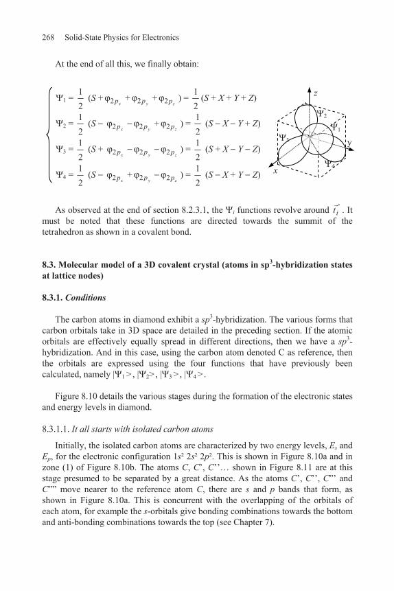
268 Solid-State Physics for Electronics
At the end of all this, we finally obtain:
1 = 12
(S + 2 xp + 2 yp + 2 zp ) = 12
(S + X + Y + Z)
2 = 12
(S 2 xp 2 yp + 2 zp ) = 12
(S X Y + Z)
3 = 12
(S + 2 xp 2 yp 2 zp ) = 12
(S + X Y Z)
4 = 12
(S 2 xp + 2 yp 2 zp ) = 12
(S X + Y Z)
As observed at the end of section 8.2.3.1, the i functions revolve around 'it . It
must be noted that these functions are directed towards the summit of the tetrahedron as shown in a covalent bond.
8.3. Molecular model of a 3D covalent crystal (atoms in sp3-hybridization states at lattice nodes)
8.3.1. Conditions
The carbon atoms in diamond exhibit a sp3-hybridization. The various forms that carbon orbitals take in 3D space are detailed in the preceding section. If the atomic orbitals are effectively equally spread in different directions, then we have a sp3-hybridization. And in this case, using the carbon atom denoted C as reference, then the orbitals are expressed using the four functions that have previously been calculated, namely | 1 >, | 2>, | 3 >, | 4 >.
Figure 8.10 details the various stages during the formation of the electronic states
and energy levels in diamond.
8.3.1.1. It all starts with isolated carbon atoms
Initially, the isolated carbon atoms are characterized by two energy levels, Es and Ep, for the electronic configuration 1s² 2s² 2p². This is shown in Figure 8.10a and in zone (1) of Figure 8.10b. The atoms C, C’, C’’… shown in Figure 8.11 are at this stage presumed to be separated by a great distance. As the atoms C’, C’’, C”’ and C”” move nearer to the reference atom C, there are s and p bands that form, as shown in Figure 8.10a. This is concurrent with the overlapping of the orbitals of each atom, for example the s-orbitals give bonding combinations towards the bottom and anti-bonding combinations towards the top (see Chapter 7).
x
y
z
1
2
3
4

Strong Bonds in Three Dimensions 269
Figure 8.10. (a) Formation of bands with coalescing carbon atoms; (b) evolution of the electronic energy levels with successive couplings; and (c) schematic illustration of orbital evolution for the associated changes in energy levels
1, 2, 3, 4 hybrid C states. Same Eh levels for the C’ hybrid states ’1, ’2,
’3, ’4. Same again for C’’, C’’’, and C’’’’. (See Figure 8.11 for definitions of C, C’, C’’, C’’’, and C’’’’).
EA= E0’+
(2) Each C atom, C’… in sp3 hybridization
EG)final=2 –4
(4) Effect of coupling between orbitals. (3) Effect of coupling
between atoms
Bonding 1L and anti-bonding 1A states between C and C’, 2L and 2A , between C and C’’, 3L and 3A, between C and C’’’,
4L and 4A , between C and C’’’’. Gives 4 bonding iL and 4 anti-bonding iA orbitals associated with the bonding EL and anti-bonding EA levels.
Increase in degeneracy due to coupling between neighboring bonding orbitals ( 1L with 2L, 1L with
3L…) and between neighboring anti-bonding orbitals ( 1A with 2A, 1A with
3A,…)
iEp
EL= E0’–i
(b)
(a)
4
2
Electronic s and plevels for isolated Catoms (2s² 2p²configuration)
Eh = Esp3 state |
state | s>
14
(Ep – Es) EG)start
Es
(1) Initially isolatedcarbon atom
Energy
Interaction energy
(EG)final (EG)start
Ep
s band Es
Eh
sp3 bonding
M p band
sp3 anti-bonding
increasing separation between carbon atoms
+ +
+
+
s And p atomic states Hybridization
states Bonding and anti-bonding states for a bond between
two adjacent atoms
Bursting into bands with coupling between
molecular orbitals.
(c)

270 Solid-State Physics for Electronics
Figure 8.11. Layout for the different atoms along
with the possible couplings using sp3-hybridization
8.3.1.2. At the critical point M
The two bands, s and p, meet at the critical point M and the s and p states mix (the so-called process of hybridization). With this hybridization being energetically favorable, we obtain sp3-hybrid states denoted by the 1, 2, 3, 4 functions for the atom C (see section 8.2). Similarly, the hybrid states for the atom C’ are represented by the functions ’1, ’2, ’3, ’4 , and so on in similar terms of notation for the C’’, C’’’ and C’’’’ atoms (for example the sp3-states of the last atom are described by the functions 1’’’’, 2’’’’, 3’’’’, 4’’’’). Each group of states, shown in zone (2) of Figure 8.10b, are represented by the functions i)i = 1,2,3,4,
’i)i = 1,2,3,4 and so on (so that there are 4N states if the system contains N atoms) with the same energy levels, as in Esp3 = Eh.
Eh can be calculated simply as, for example:
Eh = < 1| H | 1 > = <12
(S + 2 xp + 2 yp + 2 zp )|H|12
× (S + 2 xp + 2 yp + 2 zp )
= 14
{<S |H| S> + < x |H| x > + < y |H| y> + < z |H| z>
= 14
{Es + 3Ep},
where also:
Eh = < 2| H | 2 > = < 3 H | 3 > = < 4| H | 4 > = < ’1| H | ’1 > = E’0.
(Ep and Es represent, respectively, the energy levels of the 2p and 2s states; see zone (1) of Figure 8.10b).
C’’ C’ (2) (1) C C (3) (4) C’’’’ C’’’

Strong Bonds in Three Dimensions 271
We thus find that :
Ep – Eh = Ep - 14
{Es + 3 Ep}= 14
(Ep – Es). [8.12]
8.3.1.3. Initial follow-up study of the effect of type A coupling between nearest neighbor carbon atoms
This section is limited to dealing with coupling between the bonds denoted (1), (2), (3), and (4), as identified in Figure 8.12. Put in other terms, it is limited to looking at coupling effects between the bonds denoted: C–C’, C–C’’, C–C’’’, and C–C’’’’, without considering the effects of other bonds between those atoms and their other nearest neighbors. There is a formation of bonding and anti-bonding states, qualitatively described in zone (3) of Figure 8.10b, and more quantitatively detailed in section 8.3.2.
Figure 8.12. Representation of A and B couplings considered successively (obtained as a projection from Figure 8.11)
8.3.1.4. Initial study of the supplementary effect of B-type coupling (see Figure 8.12) between molecular orbitals
The coupling between (1) and (2), and between (2) and (3), and so on, that generates energy bands is shown in zone (4) in Figure 8.10b. Once again, a more quantitative approach will be developed in section 8.3.3.

272 Solid-State Physics for Electronics
8.3.2. Independent bonds: effect of single coupling between neighboring atoms and formation of molecular orbitals
Zone (3) corresponds to the states appearing following paired coupling between two atoms using the sp3 hybridization (for example between atoms C and C’). This atomic orbital coupling result in a formation of molecular orbitals for which there are solutions that can be given in the form of a linear combination of atomic orbitals (with the | > orbital for the C atom, and the | ’> orbital for the C’ atom), i.e.:
= c | > + c'| ’>.
If the direction denoted 1 represents the bond between atoms C and C’, the resulting molecular orbital ( 1) can be bonding or anti-bonding (see sections 7.1.2 and 7.1.3), as in:
1L = 12
(| 1> + | 1’ >) [8.13]
1A = 12
(| 1> - | 1’ >)
With the pairs being tied to one single carbon atom but nevertheless independent, that is to say without affecting one another, there appear (in addition to 1L and 1A) the following molecular orbitals around the atom C:
2L = 12
(| 2> + | 2’’>) and 2A = 12
(| 2> - | 2’’ >)
3L = 12
(| 3> + | 3’’’>) and 3A = 12
(| 2> - | 3’’’ >)
4L = 12
(| 2> + | 4’’’’>) and 4A = 12
(| 2> - | 4’’’’ >)
The energies associated with these bonding and anti-bonding states are the respective energies EL and EA. They have the same form as those determined in section 7.1.2, as in:
EL = E’0 - and EA = E’0 + [8.14]

Strong Bonds in Three Dimensions 273
where:
E’0 = Hii = < i |H| i> = Eh = Esp3
– = Hii’ = < i |H| i'> (coupling parameter between paired near-neighbors)
NOTE.– With N being the number of atoms in a crystal, the number of L-type bonds is equal to 2N as each carbon atom gives rise to four bonding bonds (each containing two electrons) with each being shared between two atoms (therefore on average each carbon atom has two bonding bonds).
With the number of valence electrons per atom being four (2s2 2p2 2t4, with t
representing the hybrid states), the fundamental state corresponds to the placement of 4×N electrons, and this can also be written as (2× 2N) as it represents the number of electrons per bonding orbital multiplied by the number of bonding bonds.
The consequence of this is that all bonding bonds are full and the anti-bonding
bonds ( A, that are present in an equal number) are all empty.
8.3.3. Coupling of molecular orbitals: band formation
In effect, the reasoning in section 8.3.2 highlights that for a crystal of N atoms the level denoted EL (just like EA) is degenerated 2N times (as it is for 2N bonding orbitals). The following discussion centers on the effect of coupling between orbitals on their degeneracy.
8.3.3.1. Effect of the bonding energy between hybrid orbitals around the same carbon atom
This energy can be stated as < 1 | H | 2> = – , so that with the forms given for 1 and
2 in section 8.2,
– = <12
(S + X + Y + Z | H | 12
(S – X – Y + Z)>
= 14
(Es – Ep –Ep + Ep) = 14
(Es – Ep)
The effect is apparently non-zero, meaning that in a 3D covalent crystal we should expect a non-zero coupling between the molecular orbitals bonding two adjacent atoms.

274 Solid-State Physics for Electronics
8.3.3.2. Effect of coupling between neighboring bonding orbitals in the heart of the crystal
This coupling, denoted by the letter B in Figure 8.12, has matrix elements in the form:
< 1L | H | 2L> = <12
(| 1> + | 1’ >) | H | 12
(| 2> + | 2’’ >)>
Neglecting the coupling integrals between non-adjacent neighbors (so that for example, < 1’| H | 2> 0), we obtain:
< 1L | H | 2L> = 12
< 1 | H | 2 > =1 12 4
(Es – Ep) = 2
[8.15]
By modifying the energy levels (type EL), the coupling of molecular bonds increases the degeneration by EL = E’0 – .
By analogy to the 1D model, the wave functions of the crystal need to be written,
at this level, as a linear combination of bonding ( L) or anti-bonding orbitals ( A). These functions, characteristic of a periodic lattice, should always satisfy the Bloch and Floquet theorems, and therefore should take on the form:
.Lk 0
s( ) c ( )sik r
L sr e r r
.Ak 0
s( ) c' ( )sik r
A sr e r r
These are the additive Bloch functions for bonding and anti-bonding functions. They delocalize the electrons throughout the 3D lattice, just as the equations verifying Floquet’s theorem do in a 1D system (see equation [7.16]).
Just as in the 1D systems detailed in Chapter 7 and the 3D system based on
s-orbitals described in this Chapter 8 (section 8.1), these functions result in the approximate levels EL and EA (zone 3 of Figure 8.10) breaking down into bands (zone 4 of Figure 8.10).

Strong Bonds in Three Dimensions 275
This gives rise to 2N functions of the type ( )Lk r (in fact 4N if you take spin
into account). The bond of bonding states is therefore full, justifying the terminology “highest occupied molecular orbital” or HOMO for short, otherwise known to physicists as the valence band (VB). For its part, the band of anti-bonding states, known as the lowest unoccupied molecular orbital or LUMO, and conduction band (CB) is empty. These two bands are separated by the so-called “gap” that has a height denoted EG.
In quantitative terms, we have seen in section 8.1 that for s-orbitals characterized
by the coupling parameter – = < s |H| s 1>), the width of the thus formed bands I equal to 2Z in the alternating systems (see equations [8.10]). For the example treated in Figure 8.11, the coordination number of Z is 4 and the coupling parameter is given by < 1L | H | 2L> =
2. An estimation of the width of the HOMO and
LUMO bands can thus be given by assuming that equation [8.10] is acceptable for the orbitals is acceptable, so that B 2.4.(| |/2) = 4 | | (zone 4 in Figure 8.10b).
In addition, the height of the gap can be directly evaluated from Figure 8.10b
where GE 2 4| | . The values of and depend on the cell parameters and the sizes of the atoms. For example, with the gap EG = 5.4 eV, diamond is more of an insulator than a semiconductor.
On going to the bottom of column IV in the periodic table, that is from carbon
through silicon towards germanium, i.e. with increasing atom size, there is an increase ( 4 ) in the permitted bands, so that the gap decreases (5.4 eV for C, 1.1 eV for Si, 0.7 eV for Ge).
8.4. Complementary in-depth study: determination of the silicon band structure using the strong bond method
This study comes from the work of G. Leman in “Annales de physique”, vol. 7, pages 505–533 (1962). Given the complexity of the calculations, this work is considered as a complementary study to the simplified version shown in section 8.3 that deals with diamond, that has the same structure as silicon.
8.4.1. Atomic wave functions and structures
The structure of silicon is similar to that of the carbon diamond; it is based on an inter-penetration of two fcc lattices, one being displaced with respect to the other by a quarter diagonal (see Figures 6.6b, and 8.4). The atoms represented by an empty

276 Solid-State Physics for Electronics
circle, those of the second fcc, in Figures 8.4 and 8.13 are positioned by the vector 'jr shifted by a vector b with components
4 4 4, ,d d d with respect to the jr vector,
which locates the full circled atoms of the first fcc. In effect, 'jr = jr +b . The
vectors are defined as follows so that we have a systematic and coherent set of notation:
0 1 2 3
0 / 2 / 2 00, / 2 , 0 , / 20 0 / 2 / 2
d da a d a a d
d d
The first four atoms neighboring the atom located by 'jr (belonging to the
second lattice) are located by the vectors j nr a . Similarly, the first four atoms
neighboring the atom located by jr (belonging to the first lattice) are located by the
vectors 'j nr a . Each atom located by jr (or by '
jr ) is at the center of a regular
tetrahedron, while the atomic orbitals that bond them to their closest neighbors are hybrid orbitals with a form determined in section 8.2.3.3 and denoted 1, 2, 3, 4 (the electronic configuration of the external layer of silicon is given by 3s²3p², so the
functions are obtained from the 3p orbitals instead of the 2p orbitals used in
the case of carbon). Here, the hybrid functions for the atoms located by jr or 'jr are
denoted using ji and 'ji , with i = 0, 1, 2, 3, such that:
Figure 8.13. Location of atoms in the silicon based structure
o
d
'jr
1jr a
0j jr r a
3jr a 2jr a
b

Strong Bonds in Three Dimensions 277
j0 = 12
(S + 3 xp + 3 yp + 3 zp ) goes in the direction [111]
j1 = 12
(S – 3 xp – 3 yp + 3 zp ) goes in the direction [-1-11]
j2 = 12
(S + 3 xp – 3 yp – 3 zp ) goes in the direction [1-1-1]
j3 = 12
(S – 3 xp + 3 yp – 3 zp ) goes in the direction [-11-1]
’j0 = 12
(S’ – 3' xp – 3' yp – 3' zp ) goes in the direction [-1-1-1]
’j1 = 12
(S’ + 3' xp + 3' yp – 3' zp ) goes in the direction [11-1]
’j2 = 12
(S’ - 3' xp + 3' yp + 3' zp ) goes in the direction [-111]
’j3 = 12
(S’ + 3' xp – 3' yp + 3' zp ) goes in the direction [1-11]
These functions (atomic orbitals) make up a useful base for describing tetrahedral bonds, but they are not the proper functions of a crystalline system (orbitals described by following the LCAO method). So, each function points towards a tetrahedral summit, the identity of which depends on the identity of the covalent bond being studied. Schematically, for a bond between an atom of the first lattice located by jr (= 0jr a ) and an atom of the second lattice located by '
jr
(= '0jr a ), Figure 8.14 shows the line along which runs the direction of the bond.
0j '0j
Figure 8.14. Bond between atoms located by jr and 'jr

278 Solid-State Physics for Electronics
If H represents the Hamiltonian for an atom, of form ²2m
H
( )jV r r for the atom centered on jr , we can use the calculations in sections
8.3.1.2 and 8.3.3.1, respectively:
– a matrix cell with a form given by:
0 01
| | 34
| |
j j s p
ji ji
H E E
H
– a matrix cell with a form given by:
0 11
| |4
| | , with
j j s p
ji j
H E E
H i
Evidently this gives the same results as those with the 'ji functions.
8.4.2. Wave functions in crystals and equations with proper values for a strong bond approximation
8.4.2.1. Wave functions and their properties
For a crystal and point located by r , the Hamiltonian is in the form:
2'
cryst ( ) ( ) ,2 j j
jH V r r V r r
m
where '( ) and ( )j jV r r V r r are the Coulombic potentials centered at atoms jr
and ' ,jr respectively. The wave function at a point r in the crystal, within a strong bond
approximation, must appear as a linear combination of atomic orbitals for which there is a limit in the number of cells directed towards the first four neighbors.

Strong Bonds in Three Dimensions 279
Similarly, this function should have in front of it a Bloch function and the final solution should in the (Floquet) form
. ' '
0,1,2,3( ) ( )jik r
k i ji j i ji jj i
r C e A r r A r r
where there is a sum over all sites (j) in the lattice, the index i represents one of four orbitals at a j site and C is the normalization factor. In the simplified model developed here, all ji or '
ji pseudo-orthogonal functions are considered, while
neglecting the overlap integrals (before the unit) of the type | 0ji m j
which is the overlap integral for orbitals in the same fcc lattice
centered on different atoms ( j ); and '| 0ji m which is the overlap
integral between orbitals from different lattices (for whatever , even j ).
The only overlap integrals between atomic centers taken into account are those for immediate neighbors (that also therefore belong to two different fcc lattices) and only their atomic orbitals that point directly towards one another (Hückel type approximation). The only integrals that are studied are therefore given by (wherein j and denote the first neighbors):
' ' '| ( ) | | ( ) |ji j li ji liV r r V r r
Thus 'j nr r a locates the first neighbor to that at jr towards which points
the ji function. The parameter is positive because the potentials (V) are negative
(attracting potentials). These hypotheses of course neglect completely any influence of second neighbors. So to resume, we can use and to denote the functions on neighboring atoms that point towards one another so that the strong bond approximation and the overlap integrals between immediate neighbors (Hückel) can be written, respectively as
'| 0 and ' '| | | ' | .V V

280 Solid-State Physics for Electronics
8.4.2.2. Equation using proper values
To simplify the problem, we can consider just the atom at the origin. If H is the Hamiltonian of the electron placed at the central atom, the Hamiltonian for the crystal can be:
'cryst
0( ) ( )j j
j jH H V r r V r r
Using 0i and '0i as the hybrid functions for, respectively, the atom at the
origin and the atom situated with respect to b by components 1 / 4,1 / 4,1 / 4 , we can perform a scalar multiplication on the left-hand side successively with 0i
and '0i to give the equation with proper values:
cryst ( ) ( )k k kH r E r
and obtain the two equations (with i = 0, 1, 2, 3):
0 cryst 0( ) | ( )i k k i kH r E r
'0 cryst 0' ( ) | ( ) .i k k i kH r E r
At the origin, the atomic orbital ( 00) points towards a site placed along b found (according to our simplified hypothesis) uniquely coupled with the orbital '
00 , and
with a coupling coefficient given by 0
00
. 0e 1a
ik a e . Similarly, at the origin, the 01 orbital directed along [-1-11] is only coupled with the orbital centered on the site
with coordinates (–a/4, –a/4, a/4), vector components ' ,jr b a and points
towards [11-1], so that we have the orbital given by '1,1 1( [ ])r a
'1,1 1( ).r a As '
jr = jr + ,b we here have 1,jr a and the corresponding
coupling coefficient (in the form . )jik re is 1. .ik ae By extending these results over all 0i orbitals, the two preceding equations arising from the proper values equation then give:

Strong Bonds in Three Dimensions 281
. '
. ' '
30
4 4
30
4 4
m
m
s p s p ik ak m i m
i m
s p s pik am k m i
i m
E E E EE A A e A
E E E Ee A E A A
By making ( ),k px E E ,nik an e and as stated above
4,
E Ep s
the preceding system can be written as:
'
* ' '
02 2
0.2 2
m i m mi m
m m m ii m
x A A A
A x A A
This system based on 2 4 8 linear equations (as i takes on the four values 0, 1, 2, 3) gives eight coefficients (Ai and A’i) from which the wave function k(r) can be deduced. In order to do this, we shall write that the compatibility of the eight equations necessitates that the determinant of the system is equal to zero, hence we have the following secular equation:
0
1
2
3*0
*1
*2
*3
0 0 00 0 00 0 00 0 0
0.0 0 0
0 0 0
0 0 0
0 0 0
xx
xx
x
x
x
x
By making 14
,nn a long calculation shows that the secular equation can
be written as:
2² ² ² 4 ² 4 ² 4 ² 4 0x x x x x

282 Solid-State Physics for Electronics
where is a Bloch function that depends on the k vector and is given by
1/21
( ) 1 cos cos cos cos cos cos 02 2 2 2 2 2 2
y yx x z zk a k ak a k a k a k ak
When k is directed along [100], such that y and k 0x zk k k , we
thus have cos4
ka.
8.4.3. Band structure
x can be determined using the secular equation, and then we can find the
dispersion relation ( )E k . As depends on the direction of k , the energy Ek = Ep
+ x also depends on the direction of k . The equi-energy surfaces in the reciprocal space are undulated spheres, undergoing so-called “warping”. The energy E ( Ek) is in fact a function of two parameters, on the one hand 1
4( )p sE E
which depends on the nature of the free atom, but also varies little with each type of element (between C, Si, and Ge), and on the other hand, the overlap integral ( ) for two neighbors that depends on the parameter of the crystalline lattice (d), which is in fact a function that decreases with the distance ( ) between atoms. The energy is generally studied as a function of 2 / and we can show that the electronic structure changes considerably depending on whether or not is higher or lower than 2 .
8.4.3.1. Flat bands
These relate to the solution found for the secular equation when:
2² ² 0x
in that:
1 1
2 2
(twice degenerate solution)
(twice degenerate solution).
p
p
x E E
x E E
These bands are flat in the sense that the values of E1 and E 2 of the energy does not depend on k.

Strong Bonds in Three Dimensions 283
8.4.3.2. Wide bands
These are associated with solutions other than those of the secular equation, and correspond:
– on the one hand to ² 4 ² 4 0x x , with solutions:
3 2 4 ² ² 4x
4 2 4 ² ² 4x
– on the other hand to ² 4 ² 4 0x x , with solutions:
5 2 4 ² ² 4x
6 2 4 ² ² 4x
In the direction [100] where 4
cos ,ka when k varies from 0 to 2 ,a
changes from 1 to 0 and the energies are given as solutions xi (i = 3,4,5,6) that vary
continuously from (0)ix to 2 ,aix leading to wide bands.
With k = 0, we have 5 2x and 6 2x , which shows
that when 2 we have a change in behavior.
8.4.3.3. Practical study of E = f (k), or more exactly x = E – Ep as a function of k when k is parallel to the direction [100] and for which cos( / 4)ka
Over the width of the zone, k varies from 0 to 2 / a and respectively takes on 1 and 0.
When < 2 , the solutions for x, with respect to k values, are the following (see
also Figure 8.15a):

284 Solid-State Physics for Electronics
Figure 8.15. Curves for x = f(k) when: (a) < 2 which
corresponds to having a large ; and (b) > 2 as when is small
When > 2 , the solutions for x, depending on k values, are (also see Figure 8.15b):
In Figure 8.15, we can see that when, as in the scenario (a), < 2 , the two highest and lowest bands have the same width (2 ) and the overlap integral ( ) is small. This is quite a complicated function of distance ( ) between atoms, but in general it just results in a steady decrease, even though we should state that in this case, the atoms are so far apart they could almost be called independent. Indeed at the limit of this, the energies of the atoms resemble those of isolated atoms. In the second case denoted (b), where > 2 , the two upper and lower bands have the same width (4 ). The overlap integral is large and the distance ( ) between atoms is small.
x = E – Ep
x1
x2
-2
– 4
– – 4 –2 – 4 ² ²
x
x5
x6
x4
0
k 2a
(a) < 2
empty band
x = E – Ep
x1
x2
–2 + 4 ² ²
– 4
– – 4
–2 – 4 ² ²
x
x5
x6
x4 k 2a
0
EG
empty band
(b) > 2

Strong Bonds in Three Dimensions 285
8.4.3.4. Study of band filling
Let us look at how levels fill up with electrons in practical terms. The assumption is made that in directions other than the [100] shown in Figure 8.15, the bands are similarly distributed throughout the ranges of energies. This can be compared against other works, for example, G. Fishman where the curves are traced in the directions [100] and [111], and for the same scenario as in (a) = , and then when scenario (b) is looked at, Fishman uses = 3 .
A priori, we should be able to place all 8N electrons into the system, as it was assumed that there were two electrons in each N cells, and that each atom liberates four electrons. As there are N cells, k takes on all N values with energy levels that have two places for electrons of opposing spin. Finally, the 8N electrons should fill, in both cases, the lowest 8N energy levels, as shown in Figure 8.15 for the four solutions x4, x6, and x2 (twice degenerated). Each of these four solutions, in effect, contains N levels (equal to N values of k) filled with 2N electrons, such that the four solutions can take on all the 8N electrons spread over the whole extent of the bands.
The result is that in for case (a), as shown in Figure 8.15a, the medium is a conductor as the last two occupied levels, resulting from solution x2, can easily mix their states with those of the empty levels from solution x5. Conversely, in scenario (b), as shown in Figure 8.15b, the medium is an insulator (or semiconductor) as the last occupied levels (x2) is far, in terms of energy, from EG = (2 – 4 ) of the first empty level of x5. This inhibits state mixing (that can only happen now with a high activation energy). In case (b) the two upper and lower bands have a width equal to 4 .
8.4.3.5. Study of the wave functions: the s and p characters
From the solution for the secular (otherwise termed characteristic) equation, xi, it is a simple matter to obtain the coefficients denoted iA and '
iA which give the linear combinations for the atomic orbitals that result in a determination of the wave function ( ) in the crystal.
The result, shown in Figure 8.16, is that the flat bands remain p-type (and are denoted p) over the whole of the k values (but with an evolution of the orbital linear combination
, ,3 x y zp and , ,3' ).
x y zp When k = 0, the functions are strictly s or p;
however, when k 0 they are a mix of s and p, but remain mostly either s- or p-type, and are therefore respectively denoted s0 or p0.

286 Solid-State Physics for Electronics
Figure 8.16. Generation of wave functions from atomic orbitals
for: (a) when is large (i.e. < 2 ); and (b) is small (i.e. > 2 )
8.4.3.6. Representation of energy as a function of distances between atoms
Figure 8.17 shows the energy diagram in direct space, i.e. in respect of the space between atoms.
Figure 8.17. Energy (E) (or the parameter x = E – Ep)
and the bands as a function of distance ( ) between atoms
E x
Ep 0
22
s pE E
4sE
A 2
Large < 2 metal
Small > 2
insulator/ semiconductor
Very large << 2
independent atoms
p band
p band
s0s0
s0
s0 p0
p0
p0
p0
p band
p band
2 =
EG
x = E E p
2
2
p
p
s
0
k 2 / a
Case
p
s
s
p
lar
x = E E p
p
4
4
p
s
p
sk
2 / a0
E
Case
s
p smll

Strong Bonds in Three Dimensions 287
The two places where 2 = , on either side of A, give us two types of behavior (metallic on the right where is large, and insulator on the left where is small). On the right there are two p0 bands (definitely p when k = 0, and mostly p when k 0) which are in the conduction band (CB), and two s0 bands (definitely s when k = 0, mostly s when k 0) which are in the VB. The high band for s0 is in the CB. For the two flat bands (each doubly degenerated), the upper p band is always in the CB, while the lower band is in the CB on the right and in the VB on the left.
8.4.4. Conclusion
The results shown above come from using several simplifications, such as ignoring next-nearest neighbors and an imposed hybridization on the s- and p-states in the overlap integration. More elaborate theories have made it possible to get a more accurate vision of the system. The example opposite, drawn from Chelikowsky and Cohen, Phys. Rev. B 14, 556 (1976), shows the minimum of the CB and the maximum of the VB obtained or different k values, leading to an indirect gap.
k
E ( eV)
EC
EV
EG
Figure 8.18. Silicum band scheme in agreement with Chilikowsky and Cohen
8.5. Problems
8.5.1. Problem 1: strong bonds in a square 2D lattice
For a square crystalline structure, which has a cell length denoted by a and a = 0.3 nm, there are identical atoms each tied to their neighbor by a single orbital (s in this case so as to simplify). In the approximation for the strong bond, the energy is
always written such that E = E0 – – ,mik am e where ma represents the
vectors joining the reference atom to its nearest m neighbors (here > 0, as we are dealing with s orbitals).
288 Solid-State Physics for Electronics
In reciprocal space, , X and M denote the points respectively situated at the center of the zone (wave vector is zero), at the limit of the zone in the direction [10] (such that 10 2),X G and at the limit of the zone in the direction [11] (such that
11 2).M G
1) Determine the value of the energy at the points , X and M.
2)
a) Give, for directions [10] and [11], the expressions for E = f (k) resulting from a strong bond representation, and the expressions for E0 = f (k) for an approximation for free electrons.
b) In section 5.11, problem 2, there is: 2 2
224.2
m a eV (when a 0.3 nm).
For = 1 eV and = 0.5 eV, give the numerical value that will be taken on by E0 in order that the two curves E = f (k) and E0=f (k) go through the same origin with respect to . Compare on the same scheme, for the directions [10] and [11], the evolution of the curves E = f (k) and E0 = f (k).
3)
a) Show the form of the equi-energy curves around the points .
b) Same as question 3a for the point M.
c) Give the specific equi-energy curve for E = E0 – , and state to what the curve corresponds for a system of monovalent atoms.
4) Give the form of the effective mass around the point .
5) Using the general expression for the state density function in 2D (see Chapter 2, problem 6), i.e. 1
2 ² grad( )( ) ,dL
EkL EZ E give a qualitative indication of the
form of the state density function of Z(E).
Answers
1) For the square lattice, an atom situated at the origin of the lattice has four near neighbors giving rise to four vectors denoted ma with the components:
( a , 0) along x (0, a) along y

Strong Bonds in Three Dimensions 289
Figure 8.19. Reciprocal lattice of the square structure
The facing figure shows the reciprocal lattice obtained in problem 2 of Chapter 5 with the notation used therein.
By making kx and ky the components of the wave vector ,k the energy can be
written as:
E = E0 mik a
me = E0 2 cos cosx yk a k a
For the point , we have 0,k such that kx = ky = 0, from which E( ) = E0
4 . In terms of X, we therefore have 10 2,xk k X G so that axk
and yk = 0, and hence 0 0( ) 2 cos cos 0 .E X E E For the point, we have 11 2,x yk k k M G such that .
ax yk k
The upshot is that 0 0( ) 2 cos cos 4 .E M E E
2)
a) In the direction [10] with respect to X , we have yk = 0, and the energy along y is given by:
– 010 2 cos xE E k a in the strong bond approximation;
a
a
a
a
first BZ
second ZB
102
A Ga
2B
a
direction [10]
direction [11]
X
M2
a
kx
ky
11G

290 Solid-State Physics for Electronics
– 0 210
²2 xE k
m in the free electron approximation.
In the direction [8.11] along M , we have x yk k k such that (square
lattice) 2
kx yk k and the y energy is in the form:
– 011 4 cos2
kE E a for the strong bond approximation
– 0 2 211
² ²²
2 2x yE k k km m
for the free electron approximation
b) Here we have E( ) = E0 4 and with the free electrons, ² ²
20
00.k
m kE So as to have the same origin for the energies at , we can
make E( ) = 0, and then E0 = 4 , so that with = 0.5 eV, we find E0 = 2 eV. When = 1 eV, we now have E0 = 3 eV. Numerically, with
2 2
224.2
m a eV, we have:
– 010 ( ) ( )E X E X E = 2 eV and 2 2 2
22 20 2 4.2 eV
m m axXE k
– 011 ( ) ( ) 4E M E M E = 4 eV and 2
20 2 2[ ]
m x yME k k
2 2
2m a 8.4 eV
In the graphical representation below, we can see that around the point the two curves are in good agreement. However, at the limits of the zone (points X and M), the free electrons are no longer influenced by bonds with the lattice. The band width is equal to E = E(M) – E( ) = 8 . This scheme should also be compared with that shown in Chapter 5, problem 2 for semi-free electrons in a weak bond.

Strong Bonds in Three Dimensions 291
3) The equi-energy curves are defined by the relation:
E = E0 2 cos cosx yk a k a = constant [8.16]
a) In the neighborhood of where 0,x yk k , we can write that ²
2cos 1 k ax
xk a and ( )²
2cos 1 .
k ayyk a Placing this into the preceding
equation [8.16] gives 40²
2 2 .E Ea x yk k In the reciprocal k space, E =
constant, which implies that 2 2 2 constant.x yk k k In the neighborhood of ,
the equi-energy curves are circles centered about .
b) In the neighborhood of M (where MM k and has the components
axk and )ayk the vector k has components kx and ky which can be written
such that ax xk k and ,
ay yk k where 0.x yk k From
this, ( )²2
cos cos( ) cos 1,a k xx x xk a a k a k and similarly,
cos yk a ( )²
21.
a k y Equation [8.16] thus gives:
2 2 02
4constantx y
E Ek k
a
a 2
a
E
X k10 k11
M
8 eV
4 eV
10 ( )E X
11 ( )E M
0XE
0ME
Free electrons
Semi-free electrons in
a strong bond
E0 4
E0 + 4
E0 11E
10E
010E
011E
X’

292 Solid-State Physics for Electronics
when E = constant. The equi-energy lines in reciprocal space are circles centered about
axk and ayk (components of M ) and have a radius 2 2k kx y
40E E
a.
c) When E = E0 – , equation [8.16] gives cos cos .x yk a k a As
cos cos implies that , we should here have .ay xk k In
the representation of ky = f (kx) the equation has straight slopes at 1 and an ordinate
a at the origin. The equi-energy curve, circular around , transforms
(while passing through the intermediate forms as shown in the preceding scheme) with E tending to (E0 – ) to finally bring the lines together. This results in the first zone of the square having high points at X, X1 (kx = 0, ky = ),
a X2 (kx = ,
a ky = 0),
and X3 (kx = 0, ky = ).a
This result is quite normal given that we have obtained
above [10] 0( ) ( ) .E X E X E The side of the square, equal to the half-length
of the diagonal of a square with side a
represents the Brillouin zone and thus is
equal to: 2.a
The surface of this square is thus equal to the half-surface of the
Brillouin zone and can only contain N/2 cells when the Brillouin zone contains N. This square surface of side 2
a can therefore contain N electrons, and is such that
the sides constitute the limit of the Fermi curve if the atoms making up the lattice are monovalent.
X
M
kx
ky
kx ky
a
a X
X2
X3
a
a

Strong Bonds in Three Dimensions 293
4) Around the point where k (and therefore kx and ky) is small, we can perform a limited development of the cosine functions involved in the expression for the energy:
0
2 22 22 2
0 0
2 cos cos
2 2 4 ;2 2
x y
yx
E E k a k a
k ak aE E k a
and from this it can be deduced that ²²
22 ,Ek
a such that ²2 ²
* .a
m
5) In the neighborhood of point (energy E = E0 – – 4 ), the dispersion curve is close to that of the free electrons and Z(E) should be pretty much constant in this region (as Z(E) is a constant in 2D with respect to free electrons, as detailed in Chapter 2, problems 3 and 6).
In the neighborhood of E = (E0 - ), we can use the relationship
12 ² grad( )( ) dL
EkL EZ E where L(E) is the equi-energy curve.
For free electrons, the equi-energy curve is given by L’(E) = 2 X’ (circular
equi-energy curve with radius X’, where X’ is defined in the scheme in problem 2 and is such that X’ < X). For electrons in strong bonds, the equi-energy curve has a length L(E) = 4 X 2 (square of the equi-energy curve, the side of the square being equal to X 2 ). As X > X’, in principle, we have L(E) > L’(E). All is at least of the same order of size, and the exact calculation is not of interest given the importance in the variation of |grad |k E between the two approximations, as we shall see.
In the neighborhood of E = (E0 – ), the slope of the curve E = f (k) is
considerable for free electrons, but is practically zero for (tangent horizontal in X) for electrons in a strong bond so that in this case
grad( )dL
EkL E is considerably
greater than for cases with free electrons. Z(E) for these electrons in a strong bond increases in size (at a point of singularity).

294 Solid-State Physics for Electronics
Beyond E = (E0 – ), and on coming closer to the point M (energy E = E0 – + 4 ),
the equi-energy curves for electrons in strong bonds tends to that of free electrons (circular arcs in the corners of the first Brillouin zone), and it can be expected that the state density functions for the two representations will tend towards one another. This ends up giving us the representation shown on the right.
8.5.2. Problem 2: strong bonds in a cubic centered or face centered lattices
This question first deals with a cubic centered (cc) crystalline structure (also called case 1) and then a face centered cubic (fcc) structure (called case 2). The atoms in both cases are all identical and, so as to make the problem simpler, tied to neighboring atoms only by s-orbitals. In the strong bond approximation, the energy
is still written using E = E0 ,mik am e where ma represents the vectors
joining the reference atom (at the origin) to its nearest m neighbors (and here, > 0 as we are dealing in s-orbitals). We can then go on to use the results from Chapter 6 on the cc structure (see section 6.6.1, problem 1) and on the fcc structure (sections 6.2 and 6.3).
1a and 2a) Establish the dispersion relation for both cases.
1b and 2b) Determine, for both cases, the energy values at the center of the zone, i.e. E( ), at the point X at the intersection between direction [100] and the first Brillouin zone, i.e. E(X), at the point M at the intersection between direction [110] and the first Brillouin zone, i.e. E(M), and at the point W at the intersection between direction [111] and the first Brillouin zone, i.e. E(W).
1c and 2c) Indicate for both cases the width of the band E and establish the expression for m* around the point .
E0 - - 4 E0 - + 4 E0 -
Constant
E
Z(E)

Strong Bonds in Three Dimensions 295
Answers
1)
a) For the cc structure, the reference atom (at the origin) at the highest point of the cube has eight near neighbors situated at the center of the eight adjacent cells. The components of the vectors ma joining the origin-based atom with its closest neighbors is thus of the form (associating two by two and including components with opposing signs):
/ 2 / 2 / 2 / 2 / 2 / 2 / 2 / 2/ 2 / 2 / 2 / 2 / 2 / 2 / 2 / 2 / 2 / 2 / 2 / 2 / 2 / 2 / 2 / 2
m
d d d d d d d da d d d d d d d d
d d d d d d d d
Under these conditions the energy is written (with eight terms) as:
/ 2 / 20
/ 2 / 2
/ 2 / 2
/ 2 / 2
x y z x y z
x y z x y z
x y z x y z
x y z x y z
i d k k k i d k k k
i d k k k i d k k k
i d k k k i d k k k
i d k k k i d k k k
E E e e
e e
e e
e e
from which it is deduced that:
0 2 cos cos2 2
cos cos2 2
x y z x y z
x y z x y z
d k k k d k k kE E
d k k k d k k k

296 Solid-State Physics for Electronics
b) At the point , we have 0,x y zk k k and E( ) = E0 8 . The
point X ( B on the figure shown in problem 4 of section 6.6.1) is such that X ( OB in the figure of problem 4, section 6.6.1) has the components given by:
2 ,dxk 0,yk 0.zk The result is that E(X) = E0 + 8 .
The point M is such that M ( 2OG in the figure of section 6.6.1) has the
components ,dxk ,
dyk 0.zk The upshot from all this is that:
E(M) = E0 2 [cos + cos 0 + cos 0 + cos ] = E0 .
The point W is such that W ( OF from the same figure) has the components
,dxk ,
dyk .dzk The result is that E(W) = E0 .
c) Here we have E = E(X) – E( ) = E(M) – E( ) =16 . Around where k is small, we can use the limited development of ²
2cos 1 which makes it possible
to write the energy in the neighborhood of as:
0 01 ²
2 4 4 ² 8 ² ².2 4
dE E k E d k
Thus, near , the effective mass, which is such that ²²
²
* Ek
m and here
²²
2 ²,Ek
d is therefore give by ²2 ²
* .d
m
NOTE ON THE SUBJECT OF QUESTION 1A.– The sought-after energy of problem 1a can be written with the following notation:
2( )0
, ,.x x y y z z
x y z
i d k k kE E e

Strong Bonds in Three Dimensions 297
And, in general terms, it is possible to state that:
( )
, ,
8cos cos cos 82 2 2
( )( )( )
,a b c
a b c
ia ia ib ib ic ic
ia ia ib ib ic ic
i a b c
e e e e e ea b c
e e e e e e
e
The energy for question 1a can also be written in the form:
0 8 cos cos cos .2 2 2
yx zk dk d k dE E
The results from problems 1b and 1c remain unchanged.
2)
a) For the fcc structure, the reference atom (origin) at the summit of a cube has closest neighbors at the centers of the three faces of eight adjacent cells. The three faces are along the planes Oxy, Oxz and Oyz. Each node at the center of the faces is shared with two cells and this gives in all 3 8
212 nodes that are immediate
neighbors. We can equally state that in each plane, there are four nodal “centers” so that in all there are 4 × 3 = 12 nodes that are immediate neighbors. The components of the ma vectors that join the origin-based node to the 12 neighbors are given by (again, grouped two by two):
/ 2 / 2 / 2 / 2 / 2 / 2 / 2 / 2 0 0 0 0/ 2 / 2 / 2 / 2 0 0 0 0 / 2 / 2 / 2 / 20 0 0 0 / 2 / 2 / 2 / 2 / 2 / 2 / 2 / 2
m
d d d d d d d da d d d d d d d d
d d d d d d d d

298 Solid-State Physics for Electronics
The energy written under these conditions (with 12 terms) is:
/ 2 / 20
/ 2 / 2
/ 2 / 2
/ 2 / 2
/ 2 / 2
/ 2 / 2
x y x y
x y x y
x z x z
x z x z
y z y z
y z y z
i d k k i d k k
i d k k i d k k
i d k k i d k k
i d k k i d k k
i d k k i d k k
i d k k i d k k
E E e e
e e
e e
e e
e e
e e
0 2 cos cos2 2
cos cos2 2
cos cos2 2
x y x z
y z x y
x z y z
d dE E k k k k
d dk k k k
d dk k k k
b) At the point , we again have 0x y zk k k and E( ) = E0 12 .
The point X ( H’ in Figure 6.4) is such that X ( 'OH in Figure 6.4) has the
components 2 ,dxk 0,yk 0.zk The result is that:
E(X) = E0 – 2 (cos cos cos 2 cos cos cos 2 ) = E0 + 4 .
The point M is such that M ( OM Figure 6.4) and has the components 32
,dxk 3
2,
dyk 0.zk The result is that:
E(M) = E0 – 23 3
cos cos 2 4cos2 4
= E0 + 2 2 2 1 .

Strong Bonds in Three Dimensions 299
The point W is such that W ( ',OG Figure 6.4) and has the components
,dxk ,
dyk .dzk The result is that
E(W) = E0 2 3cos 3cos 2 = E0
c) For the fcc system, we have E = E(X) – E( ) = 16 (which does not accord with E = 2Z because in this case where Z = 12 we now have E = 24 ).
The use of the limited cosine development in the neighborhood of gives:
2 220
2 22
1 ²E E - - 2 6
2 41 ²
.2 4
x y x z y z
x y x z y z
dk k k k k k
dk k k k k k
From this we deduce that
E( ) E0 12 1 ²
2 4 ²2 4
dk = E0 12 + k²d².
Once again, we obtain the effective mass: ²2 ²
*d
m .
NOTE ON THE SUBJECT OF PROBLEM 2A.– In a manner similar to that of problem 1a, we can note that for problem 2a, the following relation can be used:
,
4cos cos 42 2
( ) ( )
.a b
a b
ia ia ib ib
ia ia ib ib
i a b
e e e ea b
e e e e
e

300 Solid-State Physics for Electronics
This makes it possible to state E for the fcc system:
E = E0 4 cos cos cos cos cos cos .2 2 2 2 2 2
y yx x z zk d k dk d k d k d k d
The results for questions 2b and 2c are identical.
Comment on alternating and non-alternating structures
NOTE.– The structure of carbon diamond (based on two fcc imbricated lattices), along with its tetrahedral bonds and coordination number equal to 4, behaves different to the fcc structure.
+
+ A B
C D
+
+ C B
A
Alternate structure All closed pathways (loops) joining nearest neighbors contain an even number of atoms (square lattice, simple or cc for example). If the signs of the wave functions between A and B are reversed, and the between B and C, then C and D, the sign between the nearest neighbors D and A remains alternate. In such a structure, the most anti-bonding bond is that which has an energy equal to E0 + Z , where Z is the number of nearest neighbors.
Non-alternate structure There are pathways which are based on an odd number of atoms, for example the triangular pathway in the [111] plane of a fcc lattice. In this system the alternation of the wave function signs on a route from between A and B, then B and C, means that the sign between C and A is non-alternate. In such a structure, the most anti-bonding state thus has an energy which is below E0 + Z (and we find E(X) = E0 + 4 in place of E(X) = E0 + 12 ). The width of the band B nevertheless remains proportional to . In the fcc structure, E B = 16 . As
²,
2 ²*
dm the result is that 1*
Bm and
the mobility μ B (with the same law of variation for m* and μ as a function of B as those established in section 8.1.3 for alternate systems; only the coefficients are different).

Chapter 9
Limits to Classical Band Theory: Amorphous Media
This chapter will evaluate the limits of classical band theory, for which we have, up until now:
– assumed that there were no electronic defaults such as dangling bonds which normally arise in column IV semiconductors at the edges of finite volumes, where the covalent bond arising from one atom (C, Si) dangles away from the bulk of the material;
– neglected electron–electron (Fermi gas, or free electron gas) interactions; and – only looked at perfect, crystalline solids.
9.1. Evolution of the band scheme due to structural defects (vacancies, dangling bonds and chain ends) and localized bands
Figure 9.1 takes up where the band scheme for tetrahedral carbon shown in Figure 8.10b left off and gives a summary of the formation of valence and conduction bands in a perfectly ordered medium. As detailed in Chapter 8, the initial s2p2 configuration gives rise to the formation of four molecular sp3 orbitals, each one yielding bonding ( ) and anti-bonding ( *) orbitals. On moving to the solid state, there is a breakdown in the and * levels into bands, with the former generating the valence band, and the latter the conduction band.
Nevertheless, in a real crystal, its finite dimensions result in bond defaults. At the
end of a chain at the edge of the crystal, a carbon atom is only tied to three other carbons, and this leaves an unsatisfied sp3 bond. This is called a dangling bond, and

302 Solid-State Physics for Electronics
intrinsically contains one electron, but is electrically neutral. The electron is therefore on the Esp3 level, and the dangling bond has a localized (ELoc) level associated with it that is situated in the middle of the gap, taking into account the construction of the permitted bands (Figure 9.1).
There are other structural faults that can also give rise to similar levels in a real
crystal. These include site vacancies (generated during the preparation of the crystal), dangling bonds introduced through a physical treatment (irradiation; ionic implantation which results in bond rupture as the ions pass through the material).
Figure 9.1. The formation of localized levels associated
with dangling bonds in tetrahedral carbon
The presence of more than one structural default from dangling bonds results in an opening (for example due to the disorder created by fluctuations in bond angles) in levels in the middle of the gap as a default band. The precise position of these bands is in effect tied to the relaxation phenomena produced on formation of the defaults. It is also related to the exact origin (valence of conduction band) of the states giving rise to the defaults (dangling bond).
The lower band at the middle of the gap in Figure 9.1 thus corresponds to
a neutral dangling bond that contains a single electron. It is a donor-type band and is thus neutral in the occupied state. The upper band at the middle of the gap corresponds to the same default but exhibits a different charge state (that is that it has received an extra electron). This is an acceptor-type band that is neutral when empty. The energy difference between the two types of default is equal to the Hubbard correlation energy (U) which takes on a value given by U = <q²/4 0 rr12>. r12 Denotes the distance between two electrons on the same site. An average is made over all possible configurations. We shall now try to determine the general effect of such electronic repulsion.
E
N(E)
E
dangling bond
2s²
2p²
*
sp3
CB
VB
*-band
-band
ELoc U Esp3

Amorphous Media 303
9.2. Hubbard bands and electronic repulsions. Mott metal–insulator transition
9.2.1. Introduction
In the discussion up to now on band theory in this book, it has always been assumed that each electron moved in an average potential resulting from atomic nuclei and other electrons considered together, rather than including individual electron–electron interactions. This assumption can seem erroneous, especially when realizing that the electrostatic repulsive energy (Coulomb) is of the same order as the kinetic energy of electrons in the Fermi gas. It is thus surprising that band theories that just account for global interactions of electrons with the lattice can have the success that they have had. There are possible reasons for this, for example the assumption that the electrostatic interactions between two electrons can be screened by a conjugation of moving electrons that form a potential sphere. Other examples include the Pauli exclusion principle that largely decreases the probability of proximity between electrons. It can equally be thought that independent particles are not electrons but quasi-particles that are tied to their complementary particles (holes).
Nevertheless, there are cases where the default method is to take the independent
interactions between electrons into account. Using this method it is possible to see the transition between insulating and metallic states simply by modifying the “electronic concentration”. It is also possible to see a state predicted by band theory to be metallic to in fact be an insulator. This effect can be seen as a result of the effect of competition between kinetic and potential electron energies. For example, the metallic state is favored if the gain in kinetic energy is equal to moving electrons from the electronic state to the available empty atomic Bloch states in the conduction band (and as a consequence close to the Fermi level EF). Indeed, Heisenberg’s principle also explains this behavior because if x increases with delocalization, the V decreases; the cost in potential energy is equal to that given to the electrons so that they can overcome the electrostatic potential energy which concentrates them in the lattice. It should be noted also that this occurs with an electrostatic potential energy that is all the greater as the permittivity of the medium decreases (hence leading to an insulating material). Conversely, if the material tends towards the metallic state ( ), then the potential energy goes towards zero. This condition will be used in section 9.2.3 to derive the criteria for the Mott transition.
NOTE.– The term Fermi gas is reserved for media in which we neglect electron–electron interactions, while the term Landau liquid is used in situations where these interactions are accounted for.

304 Solid-State Physics for Electronics
9.2.2. Model
Using the Hubbard model and hypotheses, we assume that the only electron–electron interactions that are of interest are those due to two electrons on the same site (the same atom when looking at the example of a chain of atoms). This repulsive energy (Hubbard energy) can be evaluated. It can then be shown that it is considerable in certain situations, and makes possible an interpretation of the origin of some metal–insulator transitions. In order to carry out this evaluation, we shall use the example of a line of alkaline metals.
In band theory, until now, we have considered that each electron existed in an
average potential resulting from a collection of atoms and other electrons. In the case of alkali metals (Li, Na, K,…), which have one free electron per atom, the transfer of an electron from one atom to its neighbor through a conduction band occurs via electronic levels situated just above the Fermi level (EF) and the energy utilized is extremely small, of the order of a fraction of a meV.
Figure 9.2. Highlighting electronic repulsions in a chain of atoms with s-orbitals
The alkali metals shown in Figure 9.2a can be used to evaluate the problem. We will assume that overlapping between atoms is poor and the transport of electrons from one atom to the next requires a great deal of energy. Movement of an electron thus generates a supplementary repulsive energy which can be estimated by:
– calculating the ionization energy required (Ip) to separate an electron from the atom A1’ to which it is attached which subsequently becomes A1 (this change is shown in going from Figure 9.2a to Figure 9.2b);
– and calculating the energy recovered, or the electron affinity ( ) when the free electron is placed on the independent, adjacent atom A2', which subsequently becomes A2.
(a) A1’ A2’ (b)
d

Amorphous Media 305
The total energy thus required, equivalent to the repulsive energy, is UH = Ip - . For hydrogen Ip = 13.6 eV and = 0.8 eV, and thus UH = 12.8 eV, showing how UH can attain a relatively high value of several eV.
Mott showed how the repulsive energy can be calculated using r12, which
represents the distance between two electrons on the same site or atom, and (r) which is the wave function corresponding to the value proposed at the end of section 9.1:
² ( ) ² ( ² .1 2 1 24 0 12
eU r r dr drH r
Practically speaking, this energy is particularly important with respect to transition metal oxides, such as NiO, for which electron transport occurs via d-orbitals and can be written as:
Ni 2+ + Ni 2+ Ni 3+ + Ni +
For a chain of alkali metals, however, the same electron transfer, via s-orbitals, is written:
Cs + Cs Cs+ + Cs-
In Figure 9.2, A1’ A2’ Cs while A1 Cs+ and A2 Cs . When the arrows are removed from Figure 9.2 that represent the division of electrons throughout a chain of atoms, we can consider that for NiO,
A1’ A2’ Ni2+, A1 Ni 3+ and A2 Ni +
Placing an electron on a Ni2+, to form a Ni+ ion, would require the energy given by UH = I – if the Ni + and Ni 3+ ions, at positions A2 and A1 in Figure 9.2b, respectively, are sufficiently far apart, so that it can be assumed that the transported electron passes through a free state, and so that its energy En at the level n tends towards 0, as do the successive energies Ip and - , as described above.

306 Solid-State Physics for Electronics
Energy levels of isolated ions can be represented in terms of –Ip (the energy of an orbital which loses an electron, i.e. Ni3+ or A1 in Figure 9.2) and - (the energy of a supplementary electron situated on Ni+ or A2 in Figure 9.2). When the ions are well separated, as shown in the far left part of Figure 9.3, each energy level is separated by UH = Ip – which appears as a band gap between the upper and lower levels, the former having received an electron, the latter having lost one.
On bringing the ions closer to one another, as described in going from the left to
right side of Figure 9.3, transport by charge carriers becomes possible via the permitted bands which start to form. These newly formed discrete bands give rise to permitted bands (the Hubbard bands), upper level bands of electrons (in which Ni+ or A2 can be found) and lower level bands containing holes (where Ni3+ or A1 of Figure 9.2b can be found).
As the size (B) of the bands grows with increasing proximity of atoms, the
difference UH – B decreases and eventually disappears when B reaches UH (Figure 9.3). Beyond this value – obtained when the atoms are close enough to each other – the upper and lower Hubbard bands overlap and the band gap is removed; this point is also known as the Mott–Hubbard transition from an insulator to metallic state.
Figure 9.3. Evolution of the Hubbard bands as a function of band size (B):
B = 0 for atoms far apart; B = UH , where the band gap UH – B disappears to give a metal–insulator transition

Amorphous Media 307
9.2.3. The Mott metal–insulator transition: estimation of transition criteria
Different theories have been elaborated to establish, in a quantitative manner, the parameters surrounding transitions from insulator to metallic states (see problem 9.5.1). As we have seen in section 9.2.1, this transition can result from competition between localization effects, themselves resulting from electron Fermi kinetic energies (EF) and the electrostatic energies to which the electrons are subject.
To take into account the effect of the medium in which the electrons reside, we introduce into the expression for electrostatic potential a distance of action written as K1a*. K1 is a constant that takes into account the imprecision that reigns over much of the knowledge concerning interaction distances (and can be thought of as a rule of thumb), and is dependent on the hypotheses made on the various phenomena that can act, such as polarization (where K1 = r) or screening as detailed in section 9.5.1. a* is the distance that should have a form similar to a1, in that a1 = [ 0h²]/[ me²]), and is the radius of the first Bohr orbital (with the condition of taking into account the interaction with the lattice which transforms the mass of an electron to an effective mass, i.e. m*. This transforms the equation to a* = [ 0h²]/[ m*e²], so that a* = a1(m/m*).
The electrostatic potential energy (which tends to localize the electrons) must therefore be written as ²
4 *0 1.e
K aelW
For its part, the kinetic energy of metallic electrons placed on the Fermi level (EF) is written as ²
2 *2
F FmcE k (where kF is the wave number for the Fermi level
and where interactions between the electrons and the lattice are simply taken to account through m*). The number of electrons (N) contained in the Fermi sphere is equal to the number of elementary cells that are present multiplied by two so as to account for spin. This gives us:
3 3F 3
F34 / 3
2 .3 ²2 /
k LN k
L
By introducing the electronic concentration, 3/ ,eN N L we have 1/3
F (3 ² )ek N and then substituting into EcF:
2/3F
²(3 ² ) .
2 *c eE Nm

308 Solid-State Physics for Electronics
The gain in kinetic energy by the electron gas is thus 2/3²
4 ² *F 2 ,h N emcE K where
K2 is therefore a constant. The metallic state for an electronic concentration (nc) when ( ) ,
e cc N n elE W so that:
2/3
20 1
²( ) ²4 ² * 4 *
e cN nh n eK
m K a
can also be written as:
2/3
1 2 0
1 * ²*
²cm e
a nK K h
As a* = [ 0h²]/[ m*e²], this condition can be written more simply as:
21/3
1 2
1* ca n
K K
By making 1/ 21 2[1 / ]C K K we finally obtain the condition for the transition
to the metallic state:
1/3* ca n C
Experimentally, the constant C is about eight orders greater than nc. For example, an evaluation gave C 0.26, and the transition is with a* = a1(m/m*) for the effective Bohr radius:
1/3* 0.26ca n

Amorphous Media 309
Physically speaking, this criterion means that all materials can become metallic if they are sufficiently compressed so that the electron density reaches the value nc. The corresponding metal-insulator transition (M-I transition, which also occurs at n = nc) is called the Mott transition and originates from localization of electrons through electrostatic interactions, not from any material disorder. We shall see in section 9.3 how disorder alone can result in the so-called Anderson transition.
9.2.4. Additional material: examples of the existence and inexistence of Mott–Hubbard transitions
9.2.4.1. Charge transfer complexes
Charge transfer complexes (CTCs) are materials in which the effective correlation energy is high. In this case, the effective energy (Ueff) is defined as the difference between the electronic repulsion energy for a site occupied by two electrons (Uo) and the electronic repulsion energy between two electrons on adjacent sites (U1), i.e. Ueff = U0 – U1.
For a system with N sites:
– If we can assume that Ueff is negligible, each site can be occupied by two electrons (spin up, , and spin down, ). In addition, as in Figure 9.4a, if the system is half filled by N electrons then the material is metallic.
– If the system is one in which Ueff is high, we can place only one electron per site. Again, if the system carries N electrons (i.e. = 1, in which designates the number of electrons per site) then all energy levels are occupied and the band is full as shown in Figure 9.4b. Only B inter-band transitions are allowed, demanding a high energy of activation, Ea; the system, in other words, is an insulator (Mott insulator) or semiconductor. For example, the complex HMTTF–TCNQF4, in regular columns, has = 1, Ea = 0.21 eV with a room temperature conductivity
RT = 10-4 -1 cm-1.
– Once again, if the system is one in which Ueff is high and we can only place one electron per site but < 1 because bonds at the interior of each column are not fully occupied, both A intra- and B inter-band transitions are possible with the former requiring little activation energy and the latter a high activation energy. This is shown in Figure 9.4c. As an example, TTF+0.59–TCNQ-0.59 displays a metallic character with = 0.59 and RT = 103 -1 cm-1.

310 Solid-State Physics for Electronics
Figure 9.4. Electron transport with respect to electronic structure. Upper parts of the figures represent band schemes and lower parts represent
electron positions ( = occupied state, o = empty state)
9.2.4.2. -conjugated polymers
Polymers conjugated by -orbitals are, in principle, not subject to Mott transitions as transfers from one site to another in the same chain have integral values which are too high (typically of the order of 4 10 eV for polyacetylene), well above electron–electron interaction energies (U, below 1 eV for polyacetylene). Figure 9.4a therefore sufficiently describes these materials, although they do display insulating characteristics, which in the case of polyacetylene results from a Peierls distortion due to electron–phonon interactions which open the band gap (Figure 9.5).
(a) Ueff 0: electrons
in 2 states, and , allowed per site.
If system has N sites and N electrons, have
semi-full band and a metallic state.
(b) Ueff high, and only
1 electronic state allowed per site. If system has N sites for N electrons
( = 1), implies full band and material is insulator
or semiconductor and only inter-band B transitions
are allowed.
(c) Ueff high, and only
1 electronic state allowed per site. If < 1, band partially full and both A intra- and B inter-band transitions are possible.
A
A
k
E
B
B
k
E
A B
B
A
Ue
k
E

Amorphous Media 311
Figure 9.5. (a) Characteristics of -conjugated polymers, with the example of polyacetylene under a Peierls transition, verifying that U<<4 , in contrast
to (b) Mott insulators for which U>>4 (and possible for CTCs)
9.3. Effect of geometric disorder and the Anderson localization
9.3.1. Introduction
The effect of geometric disorder has for the most part been studied within theories on amorphous semiconductors developed by Mott and Davies (Mott and Davis, Electronic Processes in Non-crystalline Materials, Clarendon, 1979).
The theory is based on two fundamental ideas:
– The first idea was taken from the work of Ioffe and Regel who observed that there was no great discontinuity in the electronic properties of semi-metallic or vitreous materials when going from solid to liquid states. It was concluded that the electronic properties of a material cannot be only due to long-range order, as was proposed by Bloch for properties of crystals, but are also determined by atomic and short-range properties in which the average free path of an electron is inter-atomic. It is worth noting also that, even though a material may be amorphous, this does not exclude it from having bands. For example, glass, which is a non-crystalline material, is transparent in the visible region of light ( 1.5–3 eV), that is to say that while absorption of photons with energy below 3 eV does not occur, glass does actually have a band gap of greater than 3 eV.
molecular state
solid state: left zone of Figure 9.3
4
U
U >> 4 : scenario of Figure 9.4b
insulating state
band gap opening following strong electron-electron interactions: Mott transition
EF
(b)
molecular state
metallic solid state: right zone of Figure 9.3
4
U << 4 : scenario from Figure 9.4a
EF
Peierls transition
Band gap opens following network distortion: lower
band is full
(a)
insulating state

312 Solid-State Physics for Electronics
– The second idea is based on the evidence given by Anderson for a material without long range order that nevertheless have localized states with permitted energy bands for electrons. This theoretical model comes from observations made on certain amorphous semiconductors in which charge carriers cannot move.
9.3.2. Limits of band theory application and the Ioffe–Regel conditions
Bloch functions, i.e. ( )k r , can be used to describe electron wave functions in perfectly crystalline materials. The electronic states are delocalized and spread out over space, as denoted by 2| ( )| .k r Because of perfect delocalization, the mean free path of an electron can be considered equal to infinity.
It is only when studying a real crystal though that the mean free path of an
electron takes on significance because of effects due to quasi-imperfections caused by vibrations, called phonons (see Chapter 10), and imperfections caused for example by doping agents and impurities which perturb the regularity of potential throughout the network. It is only when these electron scattering effects, which limit the free path of electrons, are considered that the statistical average term of the free path length of an electron between two successive collisions can be introduced. In addition, there are two terms to note: “lattice scattering” which indicates collisions due to the material network; and for a similar effect caused by ionized impurities, the term “impurity scattering” is used.
On disordering a lattice by introducing vibrations and/or impurities, appears
and takes on a decreasing value as disorder increases. If there is a low amount of impurities, then local levels appear, most notably in the forbidden band (FB), but if the number of impurities increases, the localized levels grow to form impurity bands which can reach a size DEe, close to that of the valence band (VB), the conduction band (CB) and the FB introduced in Bloch’s model. Bloch's model however loses all semblance of reality when values of DEe reach the same values of the bands.
Put another way, we can go from the crystalline state to the amorphous state with
decreasing until Bloch’s theory is no longer acceptable. The limit for was fixed to k ~ 1 (for a perfect crystal, k >> 1) by Ioffe and Regel after following the reasoning of the uncertainty principle, i.e.:
E. t and x. k 1 [9.1]

Amorphous Media 313
To arrive at the result shown above, we can consider that the trajectory of an electron after a collision is random, and at the very best can only be defined between two collisions, i.e.:
( t)max = [9.2]
in which is the relaxation time – the average time between two collisions – and:
( x)max = [9.3]
From equation [9.1] we can thus directly derive the best precision in E, ( E)min, and in k, ( k)min, (1) when the equivalence of [9.1] is verified, as in E t = and
x. k = 1;, and (2) when t and x are at their highest value in equations just above and equal to ( t)max = and at ( x)max = .
We then arrive at:
( E)min. [9.4]
and:
( k)min. 1 [9.5]
The question that we are therefore brought to ask is, with increasing disorder, what are the lowest values that (and thus the mobility μ = q /m) and can go to while ( E)min and ( k)min retain acceptable values, i.e. values which are compatible with classic band theory for real crystals.
The response can be given using simple calculations which show that:
– When μ 1 cm2 V-1 s-1 (and 6 x 10 16 s), from equation [9.4] ( E)min 1 eV. Thus, ( E)min EG (band gap size) or ( E)min is the same order of size as the permitted bands. When μ 1 cm2 V-1 s-1, the uncertainty in the energy of the carriers tends to the same order of size as the permitted and forbidden bands, to such an extent that the band scheme loses its relevance to real systems. It will be shown though that the Anderson model band scheme has to take into account localized bands with a gap which eventually becomes the mobility gap, Eμ.

314 Solid-State Physics for Electronics
– When a few ångström, that is to say a, in which a is the lattice constant and is typically of the order of 3 × 10⁻⁸ cm, equation [9.5] results in ( k)min
1/ 1/a 3 × 107 cm-1 k. In effect, with = h/mv in which v = vthermal 100 km s-1 and 7 × 10⁻⁷ cm, we have k = 2 / 107 cm-1. We can directly infer that in the band scheme, conduction electrons will be such that k 1/a. At these values, where a, we thus have ( k)min k, and k can no longer be considered a good physical parameter to which we can apply quantification. In addition, when k ~ k, Fermi's sphere is badly defined (to the point of being totally deformed) and the concept of carrier speed looses significance as k = m*v, just like the mean free path which is expressed as a function of v, i.e. = v .
Finally, as soon as a, and more strictly speaking as soon as a that
occurs when the interaction between an electron and the material network becomes increasingly strong, an electron no longer goes any further than the limits of the atom to which is tied. The electronic wave function localizes over a small region in space and is generally supposed to diminish exponentially with respect to R (as exp(– R)).
The work of Mott and Anderson has introduced a new concept of localized
states. The permitted density of states, N(E), always results in an energy band beneath a single EC for a conduction band and above a single EV for a valence band, and, in other words, an activation energy is necessary for carriers to pass from one state to another with an emission or absorption of a phonon.
9.3.3. Anderson localization
9.3.3.1. The model
Systems in which disorder is due to a random variation in the energetic depth of regularly spaced sites (with interstitial distances always equal to a) are considered in Anderson’s model, and can relate, for example, to a random distribution of impurities. Different authors, including Mott, have tried to take into account lateral, spatial disorder and the results have been close to those of the Anderson model, to which we will limit our discussion.
In Chapters 1 and 3, we saw that if we take into account effects resulting from
a network of atoms at nodes by constructing a regular distribution of identical potential wells, then a permitted energy band of height B appears, as shown in Figure 9.6.

Amorphous Media 315
Figure 9.6. Regular distribution of identical potential wells and permitted band
Section 8.1 showed that in the strong bond approximation:
– B = 2Z , where Z = the number of adjacent neighbors, and is the resonance integral between two adjacent sites; and
– m* = ²
2 ²a =
²²
Za B
[9.6]
so that μ = ²²
,q a BZ
and semiconductors possessing a narrow B band exhibit low
mobilities. For Anderson’s model we can replace the preceding distribution (Figure 9.6) by
one of randomly deep potential wells which represent disorder, as shown in Figure 9.7.
Figure 9.7. Periodic distribution of wells with random depths
9.3.3.2. Variation in wave functions with respect to V0/B (Anderson) and (Ioffe and Regel)
We will show here how permitted energy bands change into localized states if V0/B goes beyond its critical value. In order to do this, we need to look at the following scenarios:
V a E
N(E)
B
V E
N(E) V0

316 Solid-State Physics for Electronics
– Real crystal: V0/B is very low and is high. In this case, the wave function is given using Floquet’s theorem (equation [7.19]) which can be written with the normalization constant:
0( ) ( - )nikrk n
n
r e r r [9.7]
The mean free path can be estimated from the Born approximation, by realizing that the wave vector of an electron (kn) changes to km once the electron has undergone a collision of probability Pmn and that Pnm = 1 = ,v and in addition Pnm is
given by Fermi’s “golden rule”: Pnm = 1 24
2ave ( )mN E (see Mott and Davis),
where here ave = (V0/2) and the relation is given for a unit volume. For
conduction electrons, for which Em EF, spread throughout a volume V = a3 with a distribution of wells with random depths but averaging around V0/2, we here have:
1= nmP
v=
2301 2 ( )
4 2FV N E
av
[9.8]
where N(EF) is the density of states at the Fermi level and v the velocity of an electron at the Fermi level. As is large, the system is almost a perfect crystal, and therefore it is possible to state that:
N(E) = 3/ 2 1/ 2
34 (2 *)m E
h and v =
1/ 22 *E
m
Using equation [9.6] for the effective mass, equation [9.8] gives 2/0
32 ,Va
and with B = 2Z :
202 /
32
ZV Ba [9.9]
– When (V0/B) 1 (lowest disorder) corresponding to a , i.e. threshold disorder. When a, equation [9.9] written for a cubic system in which Z = 6 results in (V0/B) = 0.83 1. At this point when a (and V0 B), the disorder is such that k k (following Ioffe and Regel), and under such conditions, at each

Amorphous Media 317
collision, k randomly varies by k, the closest neighbor to k. In going from one potential well to the next, the wave function in equation [9.7] randomly changes and, according to Mott, loses its phase memory. It should thus be written in the approximate form:
0( ) ( - )k n nn
r A r r
with An = cn exp(i n), where An is a function with a random phase and practically constant amplitude.
Moreover, this amplitude is more constant than the variation between depths of
neighboring potential wells, i.e. V0 is low in Figure 9.7. In a model using two wells with potential depths V1 and V2 (as in Miller and Abrahams, 1960) the resulting wave function can take on either a symmetric or antisymmetric form, respectively,
S = A1 1 + B 2 or A = A1 1 - B 2 . We can therefore show that when V1- V2 << | | (i.e. V0 is low), so A1 A2, the difference in energy (E1 – E2) between the two possible states is such that 1 2 E E 2| |. A representation of this function is
shown in Figure 9.8a for a network of several potential wells.
– When (V0/B) > 1 (V0/B) (just above threshold value): initial delocalization and medium disorder. In a system which corresponds to a great increase in disorder, and for the model of just two wells corresponding to an increase in the depth between the wells as in 1 2 0| – | ,V V V the difference in energy, 1 2| |,E E increases to a corresponding level and A1 differs from A2. The amplitudes of the functions are no longer constant and the wave function displays increasing disorder both in amplitude and in phase (Figure 9.8b).
– System in which (V0/B) >> 1 ((V0/B) well above threshold value): considerable delocalization and disorder. In this system a highly localized state is formed, as shown in Figure 9.8c, and as V0 increases the localization is accentuated. In addition, there is no longer propagation along a line of potential wells and states are thus localized. An exponential decrease in the wave function starts to appear and is increasingly noticeable with increasing values of V0. The wave function takes the form:
0( ) ( ) rn n
nr A r r e

318 Solid-State Physics for Electronics
from which it is possible to write:
0( ) ( )
r
n nn
r A r r e [9.10]
where is the localization length.
Figure 9.8. Variations in wave functions with delocalization: (a) delocalization–
localization only; (b) weak delocalization; and (c) strong delocalization
To conclude, the factor V0/B is a crucial term in deciding whether only localized states form (V0/B > 1) or whether both localized and delocalized states can co-exist (V0/B 1).
r
V0/B 1 and a, orbitals just delocalized
r
V0 > B
initial localization E Ec
r
V0 >> B strong localization E << Ec
(a)
(c)
(b)
| |²

Amorphous Media 319
9.3.3.3. Band scheme and form of the state density function N(E)
From a realistic scheme of the distribution of potential wells, we can see that states should be localized within one energy domain and delocalized in another. Accordingly, Figure 9.9 describes a system with non-negligible disorder:
– all states at the tail end of the function N(E) which correspond to a high enough value of V0 and from energies E < Ec and E > E’c appear localized as before in the scheme of potential wells; and
– however, the middle of the band corresponds to shallow states with small V0, such as V0/B, and is a zone of delocalized states which have E’c < E < Ec.
Figure 9.9. Representation of localized and delocalized states in co-existence
9.3.4. Localized states and conductivity. The Anderson metal-insulator transition
9.3.4.1. Mott’s definition
Mott’s definition is based on continuous conductivity relative to electrons with a given energy ( E(0)) and delocalized states are on average, at T = 0 K, those for which E(0) is zero, i.e. (0)E = 0. To arrive at an average though, all possible configurations which have the energy E need to be considered, and while some electrons may have a non-zero energy, the average over all possible states with the corresponding energy E gives zero as a result. These states and the mobility they represent are in effect thermally activated.
However, at T = 0 K, delocalized states average to give E(0) 0, that is to say
metallic behavior occurs.
V
V0
band tail (localized states)
N(E)
E
Ec Em E’c
N(E)
E
zone of delocalized state
Em

320 Solid-State Physics for Electronics
9.3.4.2. State properties
In Figure 9.9, two types of states – localized and delocalized – are separated by energies Ec and E’c which together are called the mobility edge. In the two zones Einstein’s relation holds true if EF is outside the bands of non-degenerate states. We thus have μ = qD/kT, but the diffusion coefficients (D) have different forms. Here, D = Pa² in which P represents the probability of movement to neighboring sites. This brings us to the origin of the expressions used in courses on electronics and materials:
– When E > E’c and E < Ec , D = (1/6) ph a² exp(-w1/kT) (with ph being the phonon frequency and w1 the energy of activation) and < E(0)>T=0K = 0. Here as T
0, we can verify that D and μ tend towards zero, as does the conductivity.
– When Ec < E < E’c, D= (1/6) e a² and E(0) 0 where e is the frequency of electronic vibrations.
9.3.4.3. Distinction between insulator (or semiconductor (SC)) and a metal in a slightly disorder material (poor localization and small )
Figure 9.10. Metallic character resulting from the position of EF
As for classic (crystalline) materials, the properties are tied to the position of EF (as shown in Figure 9.10):
– when EF is situated in the domain of delocalized states, (Ec < EF < E’c), we have a degeneration corresponding to a metallic character; and
– however, when EF is situated in the zone of localized states, where typically E < Ec, charge carriers can only be thermally excited and conductivity can occur only by jumps or by excitation to Ec, and indeed at 0 K conductivity tends towards 0 which is typical of an insulator. Materials for which the Fermi level is situated in an energy zone in which states are localized are called Fermi glasses.
position of EF determines the
insulating or SC character
Ec Em E’c E
N(E) position where EF gives a “metallic” character
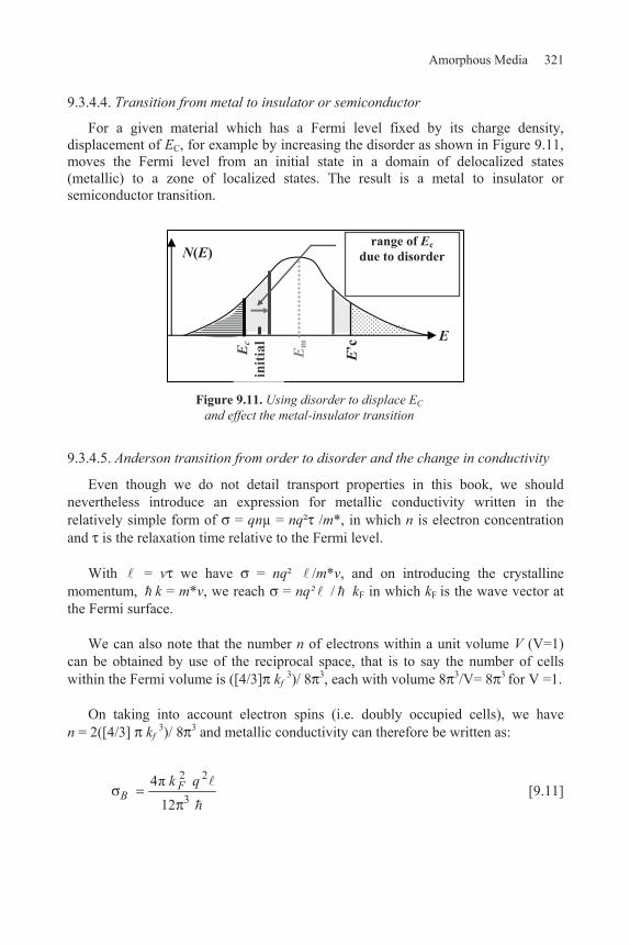
Amorphous Media 321
9.3.4.4. Transition from metal to insulator or semiconductor
For a given material which has a Fermi level fixed by its charge density, displacement of EC, for example by increasing the disorder as shown in Figure 9.11, moves the Fermi level from an initial state in a domain of delocalized states (metallic) to a zone of localized states. The result is a metal to insulator or semiconductor transition.
9.3.4.5. Anderson transition from order to disorder and the change in conductivity
Even though we do not detail transport properties in this book, we should nevertheless introduce an expression for metallic conductivity written in the relatively simple form of = qnμ = nq² /m*, in which n is electron concentration and is the relaxation time relative to the Fermi level.
With = v we have = nq² /m*v, and on introducing the crystalline momentum, k = m*v, we reach = nq² / kF in which kF is the wave vector at the Fermi surface.
We can also note that the number n of electrons within a unit volume V (V=1) can be obtained by use of the reciprocal space, that is to say the number of cells within the Fermi volume is ([4/3] kf 3)/ 8 3, each with volume 8 3/V= 8 3 for V =1.
On taking into account electron spins (i.e. doubly occupied cells), we have n = 2([4/3] kf 3)/ 8 3 and metallic conductivity can therefore be written as:
2 2
34
12 F
Bk q
[9.11]
E
N(E) E
cin
itial
range of Ec due to disorder
E’c
E m
Figure 9.11. Using disorder to displace EC and effect the metal-insulator transition

322 Solid-State Physics for Electronics
Figure 9.12. Anderson’s transition from metal to insulator at absolute zero following 1/(V0/B) = B/V0 . The same behavior occurs when EF is displaced with respect to EC
When considering a metallic state, the Fermi level can be considered more or less in the middle of the band (so that in 1D, kF /a) as shown in Figure 9.10. With increasing disorder, Ec and E’c tend towards each other at the band center Em ( EF) in which case all states are localized. This change is called Anderson’s transition, as shown in Figure 9.12.
At the same time, we have V0/B 1 with tending towards a. For its part, with
= a, conductivity thus tends towards min = IR = ( B)l =a= q²/3a . In mono-
dimensional media this abrupt transition is a point of controversy as it is known to occur progressively in 3D. When a is of the order of 3 Å, IR = 700 S cm-1, it is often a value of saturation for conductivity in rising temperatures.
9.4. Conclusion
This chapter has shown how supplementary effects, defaults in the periodicity, caused by such as dangling bonds, chain-ends and holes within the structure introduced into the band gap localized levels can open to form a band when their fluctuation is brought into account. This band can split as a function of electron filling, in a manner analogous to the perturbations caused by electron repulsions, which were not taken into account in the band theory. These electronic repulsions were looked at in detail and we have shown how they can help to explain metallic or insulating behaviors that the classic band theory cannot deal with.
By introducing modifications of crystal regularity by considering network
thermal vibrations (phonons) and defects, both chemical (impurities) and physical
Ec
T = 0 ; μ 0 ; 0 (metal)
metal–insulator transition
ln
(B /V0) or EF
1D 3D scale law
T = 0 μ = 0
= 0 min
increasing disorder
EF Fermi glass

Amorphous Media 323
(dislocations), the notion of a real crystal was studied. This resulted in determining the mean free pathway of electrons, which can no longer be considered as completely delocalized within the network – as in the case of a perfect crystal. It was shown that an increase in disorder reduced the mean free path length up to the point of localizing electrons in neighborhoods of deep defaults, resulting in energy levels localized at extremities, or “tails”, of permitted bands.
Figure 9.13. Band models for amorphous semiconductors: (a) following CFO; (b) following μ(E) at T = 0 K; (c) following μ(E) at T > 0 K; (d) following Mott and Davis
Finally, it can be noted that all models postulate for amorphous media, such as crystalline semiconductors, that there are conduction and valence bands which are or are not separated by a band gap, depending on the all-important band tails. And that:
mobility gap
tails of delocalized states
EV EB EF EA EC
μ(E)
E
N(E)
E
μ(E)
E
T = 0 K
T > 0
N(E)
E
(c)
(b)
(a)
(d)
conduction band (CB) of
delocalized states BV

324 Solid-State Physics for Electronics
– Bands result in part from short-range order (from approximations of strong bonds giving rise to bonding and anti-bonding states, i.e. valence and conduction bands separated by a band gap) and from disorder created by phonons or impurities shown by tails of delocalized states. Tail states are neutral when occupied in the case of the valence band and when empty in the conduction band. The Fermi level is thus placed in the middle of the band gap, as shown in Figure 9.13a and following the model proposed by Cohen, Fritzsche and Ovshinsky (Frizsche, 1970).
– The form of the bands depends on the type of the implicated orbitals. For p or d orbitals, which are less stretched overall into space than s-orbitals, the form of N(E) is different and the bands are smaller.
– In a perfect crystal, the band gap is an forbidden energy in which N(E) = 0, while in an amorphous material it is a mobility gap and N(E) is not necessarily zero but the mobility μ(E) however does becomes zero at T = 0 K (localized states), as shown in Figures 9.13b and c).
By taking into account the disorder caused by not only phonons and impurities
but also by structural defects such as dangling bonds and chain ends, additional offsetting defaults localized in the middle of the band can generate two bands at compensating levels (Hubbard’s bands) following the model of Mott and Davis as shown in Figure 9.13d.
9.5. Problems
9.5.1. Additional information and problem 1 on the Mott transition: insulator–metal transition in phosphorus doped silicon
9.5.1.1. Additional information: evidence for the Mott transition in phosphorus doped silicon
The Mott transition can be illustrated by way of the conductivity of silicon at low temperatures as a function of the concentration of phosphorus atoms (see Figure 9.14).
Substituting silicon atoms, four or five electrons in the external phosphorus layer
are engaged in covalent bonds with neighboring silicon atoms; the fifth electron dopes the silicon. When T = 300 K, we have kT 0.024 V so that the bonding energy of this fifth electron is of the order of 0.045 eV and the P atoms are easily ionized to P+ at ambient temperatures. The phosphorus plays the role of a donor for n-type doping of silicon.
At very low temperatures though, kT is very small as the phosphorus electrons
are tied to the P+. The fifth electron therefore tends to follow a Bohr radius calculated in section 9.2, as in a* r a1(m/m*), which in silicon is given by

Amorphous Media 325
*a 25 Å. The material is therefore an insulator in the domain of very low temperatures, at least when concentrations of phosphorus are below a critical point (found experimentally to be around 3.8 × 10¹⁸ P atom cm-3). An abrupt insulator–metal transition is found around this concentration.
It is possible to consider that at high concentrations of phosphorus atoms, their orbitals overlap so that electrons can pass by tunneling from one P+ ion to another. The resulting electronic cloud can play a role as electrostatic screen between the P+ and the fifth electron so that the latter end up being delocalized in the cloud. Once this process of liberation (with respect to the atom of origin) has occurred, it gains strength through a growing screening effect.
9.5.1.2. Problem: the Mott transition as an equation and its resolution
The mechanism for the Mott transition can be characterized physically in the following manner: if a nucleus with a positive charge (denoted here Ze ) is placed in a free electron gas, the electrons will be attracted to the positive charge and generate in the neighborhood of the nucleus a surplus negative charge density. This negative space charge will then screen the positive charge and the potential generated by the nucleus (
4 00 )Ze
rV in the vacuum will be reduced so that in the material,
Figure 9.14. Conductivity of silicon doped with phosphorus near absolute zero
concentration in donor phosphorusatoms (units = 1018 cm-3)
(0)
(1 c
m1)
10 2
10 1
1
102
10
103
0 2 4 6 8
metal insulator

326 Solid-State Physics for Electronics
4 0.Ze
rrV Parameter r is introduced to account for the nature of the material. If
it is a dielectric, the electronic charges are tied by covalent bonds to the cores of the ions and are, as a consequence, not very mobile. The “screening” is therefore poor and r is small (typically of the order of two or three). If the medium is metallic, the electrons are very mobile and the screening effect can be complete some distance from the nuclei. In such cases, V 0 and therefore r (total “screening”).
Nevertheless, this screen is effective right from the very shortest distance, of the
order of an ångström. At greater distances the electrons no longer see the potential of the nuclei and it is for this reason that electrons behave independently from the nuclei at distance greater than the screen. It is this distance that we will try to evaluate.
The most mathematical treatment of the screen effect can be carried out within
the Thomas–Fermi approximation. It is assumed that the local perturbation created by the electronic cloud has a potential V (generated by the positive charge) and reduced locally by the energies of the electrons by dE = |e| V. The result is that the electronic density function is modified by n.
1) Express n using the density of states function in EF (function Z(EF)).
2) Write the Poisson equation that ties n and V at a point far from the positive cores.
3) Assuming that the medium is isotropic, the perturbation potential can be thought of as being constant for a given r, i.e. it has a spherical symmetry. Write the Poisson equation for these conditions.
4) Give the physical solution to this differential equation by introducing the
parameter ²
0
1/ 2
F( )eTF Z E which is the Thomas–Fermi screening length.
5) Determine the solution using the limiting condition that V tends towards the Coulombic potential as TF . Make a comparison using a graphical representation.
6) Give the equation for the spatial variation in the dielectric permittivity.
7) Express TF as a function of the electronic concentration (Ne) and the parameter a* = a1(m/m*) (where a1 = [ 0h²]/[ me²]).
8) What relation should one have between a* and TF for the medium to be considered metallic? From this deduce the relation that gives the critical electronic concentration (nc) above which the medium is metallic.

Amorphous Media 327
Answers
1) If a local perturbation V (by an electronic cloud) of the potential reduces the potential energy of the electrons by dE = |e| V, the electronic density is modified by n = Z(EF) dE = Z(EF) |e| V, where Z(EF) is the density of states function (or state
density function – the term is interchanged in this book) at the Fermi level (EF), the level at which the conduction electrons are transported.
2) Far from the cores of the positive charges, where the volume density of the charge is = e n, the Poisson equation that relates n and V is
00e nV (with the medium of the material being represented by charge
that bath in a vacuum, the permittivity being used is thus 0). With n = Z(EF) |e| V we thus find:
F0
²( ) 0
eV Z E V
3) Supposing that the medium is isotropic, the potential due to the perturbation ( V) can be assumed to be constant for a given r, that is within a spherical symmetry. In this case, the Laplacian is in the form:
²²1 2 1²
² ² ²
r VV V Vr
r r r r r r r r
so that the Poisson equation takes the following form:
F0
² r V1 e²Z(E ) V 0
r r²
which can then be written in the form of a classic differential equation:
F0
² r V e²Z(E ) r V 0
r²

328 Solid-State Physics for Electronics
4) The solution for this differential equation is:
1/ 2 1/ 2² ²
0 0( ) ( )
[ ( )]F F
e eZ E r Z E r
r V Ae BAe
so that:
1/ 2 1/ 2² ²
0 0( ) ( )
.
F Fe e
Z E r Z E re e
V A Br r
As:
lim ,x
mx
e
x
with m > 0, the second term diverges and we have to take B = 0, so that:
1/ 2²
0( )
.F
eZ E r
e
rV A
By making the hypothesis, ²
0
1/ 2( )e
TF FZ E for the Thomas–Fermi
screening length we thus find .TF
r
er
V A
5) In the exponential, if r 0, or what comes to the same thing, if ,TF for an infinitely long screen, the potential must tend towards that produced by one single atomic core, that is its normal Coulombic potential, such that:
0,
4
r
e A ZeA
r r r from which
0.
4Ze
A

Amorphous Media 329
Finally, we have:
TF
r
0
eV Ze .
4 r
The electrostatic potential therefore decreases much more rapidly with distance than if it were simply the Coulombic potential.
6) In a representation of the medium with the help of the dielectric permittivity, 0 r, where r is the relative dielectric permittivity, and takes into account the
polarization of the medium, the potential generated by the charge Ze is given by
4 0.Ze
rr Identification with the preceding form of the equation,
4 0,
r
TFer
V Ze
gives .TF
r
r e It is possible to see that when r >> TF, r . This result is normal as in this region the electrons are not subject to any
influence from the charge Ze, which would tend to localize them. When r >> TF the electrons are free as in a metal, for which the permittivity also tends towards infinity.
+Ze
TF
External zone where the generated potential is screened by the electronic cloud
zone of poor “screening”
Coulombic potential zone with a long radius of action
r TF
V
VCoulombic
V
VC( TF)
( )C TFVe
330 Solid-State Physics for Electronics
7) In addition, 3/24 (2 *)
3( ) m
hF F c FZ E E A E , where
3/24 (2 *)3
m
hcA
2 *2
3/ 24 ,m
h and where EF can be expressed as a function of the electronic density
by writing, for example, that at absolute zero (see problem 4 in Chapter 2):
1/ 2 3/ 2
0 0
2( )
3
F FE E
e c c FN Z E dE A E dE A E so that 2/3
3,
2e
Fc
NE
A
from which
1/32/3 3
( ) .2F c eZ E A N
The result is that:
1/3 1/61/ 21/60 0
2/31 2 1 1 ²
3 ,3 2 ² *
TF eec
hN
e NA e m
so that with a1 = [ 0h²]/[ me²] and a* = a1(m/m*):
1/61/61/ 2 3* *0.5 .
2 3TFe e
a aN N
8) The condition for electronic behavior is that a* (which gives the position of the electron in its orbit) is greater than the screening length. This is because above this distance, the electron is no longer held by its starting atom. The result is the condition * .TFa

Amorphous Media 331
This condition is fulfilled when Ne attains a critical concentration ( ) *cn a 1/2*1
1/32,a
nc so that:
1/3 * 0.25cn a
in a condition practically identical to that found in section 9.2.3.
9.5.2. Problem 2: transport via states outside of permitted bands in low mobility media
1) What is the condition that the width of the B band of a material must verify for the effective mass approximation to be valid when used in an expression for mobility?
2) Considering a system where the permitted bands are wide (such as in -conjugated polymers), of the order of 1 eV, and where the mobility is of the order
of 10–3 cm² V–1 s-1. Can electronic transport occur in the permitted bands?
3) We now consider solids as molecular solids where intermolecular bonds are through weak van der Waals bonds. Can it be said that this system has a narrow band? In this example where the mobility can be taken as being in a general form (for a 1D system), ,q
kT xv and where it may reach 1 cm² V–1 s–1, does the
transport occur through these narrow permitted bands? Using the example of anthracene, the intermolecular distance is given by a 6 × 10⁻⁸ cm. For cases where we know the resonance integral ( 0.01 eV for anthracene), give an alternative rationale.
Answers
1) To define the effective mass, as in section 8.1, the width (B) of the permitted bands must be such that B >> kT, or otherwise the band width will approach kT (0.0026 eV at ambient temperature), and it will not be just the lowest levels of the band that are occupied but all possible levels that can be taken up through thermal agitation. The form of the mobility for a strong bond is no longer acceptable. Expression [8.11] from Chapter 8, μ = ²
²,q a B
Z obtained with the help of the classic
expression for mobility *
,qm
μ in which is introduced the effective mass

332 Solid-State Physics for Electronics
²²
*Ba
m Z (see equation [8.11’] where Z is the coordination number). In effect, to
obtain this expression for m*, we use an approximation that excludes the states at the base of the band (k 0, and situated at the center of the zone for which E is
a minimum, so that 0
0Ek k
also allows the limited development over cosines
which is involved in the expression for a strong bond).
2) From the preceding section the approximation of the effective mass is valid when considering wide bands, for example HOMO and LUMO bands in
-conjugated polymers. Inside these bands, the carrier mobility can be evaluated with the help of the equation μ = ²
².q a B
Z
In addition, and as has been detailed in this chapter (see section 9.3.2), for bands
to retain a physical significance B > E, where E (equation [9.4]). Under these
conditions for there to be conduction in these large bands of delocalized states, we should also verify that:
²²
q a Bμ
Z>
²²
q a EZ
² 1
.qa
Z
This equation, μ > ² 1 ,qaZ
is the condition for conduction in the B bands of
delocalized states. With a several Å (length of strong bonds in -conjugated polymers) and Z 2, we find the condition: μ > 10–1 cm² V-1 s–1. As the mobilities in -conjugated polymers are of the order of 10–3 cm² V–1 s-1, we can conclude that it is not reasonable to expect the transport observed in these materials to be in the bands of delocalized states. As a consequence, we can think that in such polymers, the mobility associated with delocalized states is greatly reduced by charge transport through more localized states.
3) Molecular solids give rise to narrow permitted bands, as the intermolecular bonds are through weak bonds, for example van der Waals bonds. The poor overlap of intermolecular orbitals results in low values for the overlap integrals ( ). The width (B) of the permitted bands being of the order of several (B = 2Z , see equation [8.10]), means that the system is based on narrow permitted bands. In this case, and taking the argument developed in answer 1 into account, the approximation for the effective mass used to evaluate the mobility is no longer acceptable.

Amorphous Media 333
We can therefore use the following expression for mobility: .qkT xμ v As
the speed can be given (in a dualistic theory) by ,kgv v so that with E
and in 1D we have 1 .Ek x
v With E B while k 1/a (order of size of the
Brillouin zone in the reciprocal space and corresponding to the height of the permitted band (B) (see the representation of E = f (k) in Chapter 4) we thus have:
vx ,Ba
so that .q Ba
μkT
At this level we can reason in one of two ways (which lead, of course, to similar conclusions). Either:
– we consider that to have conduction in the localized states, we should have > a (Ioffe and Regel’s second condition – see section 9.3.2), which means that:
μ > ²qa B
kT must be true.
In these small molecules, with the band width B kT, we find the same condition as in polymers:
μ > ².
qa
Taking a 5 × 10⁻⁸ cm, we should have μ 1 to 10 cm² V–1 s–1. It should be noted that here a represents the intermolecular distances that are slightly longer than the covalent bonds , so that we can reasonably state that a2 for small molecules is at least an order greater than for polymers. With μ 1 cm² V–1 s-1 and a 6×10⁻⁸ cm for anthracene, we do not find that the inequality is verified, which shows μ 5 cm² V–1 s–1; or
– we consider that we know the mobility (μ 1 cm² V–1 s-1 for anthracene) and given that B (where the resonance integral 0.01 eV for anthracene), and with a 6×10⁻⁸ cm, we can therefore estimate with the help of ,q Ba
kTμ which
gives us 3×10⁻⁸ cm. The mean free pathway appears to be less than the intermolecular distance a, which again is not compatible with conduction in delocalized states (Ioffe and Regel).

This page intentionally left blank

Chapter 10
The Principal Quasi-Particles in Material Physics
10.1. Introduction
In a physical system there are a variety of particles that exist under constant perturbation, even excitation, due to external forces that are mostly interacting with the lattice. A slightly perturbed or excited state can dissipate into elementary perturbations (excitations) that propagate through the lattice just like a particle with a degree of energy, movement, and even a spin moment. A change in the perturbed (excited) state of a material can be described using variations in these parameters of energy, movement and so on. And these variations can be due to collisions between quasi-particles that can also be described using the same parameters. These quasi-particles are the result of interactions (perturbations and excitations) between real particles or the same particles with the lattice.
Depending on the nature of the interactions, the quasi-particles can be, for
example:
– phonons: these describe the state of a lattice in which the atoms are excited by thermal vibrations. The main applications are in the domains of materials and thermal properties;
– polarons: these appear when accounting for coupling between electronic charges and the resulting lattice deformations. They are well evident in descriptions of transport phenomena in materials with low mobilities;

336 Solid-State Physics for Electronics
– excitons: these are coupled electron-hole pairs with energy levels in the neighborhood (but outside) of the permitted bands. They are essential to descriptions of the optical properties of materials;
– plasmons: these detail the collective oscillations occurring in an electron gas. There are other quasi-particles that can be present. These include polaritons, that
describe the transverse optical coupled modes of photons and phonons, magnons, that describe systems based on coupled spin moments, and solitons that correspond to a default in the conformation of a chain of atoms that may or may not be coupled to a charge. However, this text will detail only the main types of quasi-particles.
10.2. Lattice vibrations: phonons
10.2.1. Introduction
With the bonding forces between atoms being finite, an external perturbation such as thermal energy can result in atoms being distanced from the equilibrium position.
In this example the forces and atomic displacements are directed along r. With
F(r) denoting the bonding force on an atom at r with the corresponding potential energy W(r), then:
( ) grad ( ) dWF r W rdr
If r0 represents the equilibrium position of an atom (located with respect to the origin of the displacements), and if r denotes the displacement that is such that
0r r r , we can write that:
0
01 ²( ) ( ) ²2 ² r
d WW r W r r
dr
(as the first derivative is zero with respect to r0 where W(r) is a minimum and an equilibrium position). The result is:
0
( ) ²( ) ,² r
dW r d WF r r k r
dr dr when
0
²² r
d Wk
dr

The Principal of Quasi-Particles 337
and we have Hooke’s law. With dr d r , the fundamental dynamic equation is written as:
²²
d rm k r
dt
for which the physical solution is of the form:
cos cos 2kr A t A t
m
where 12
.km
This represents the sinusoidal oscillatory movement with
frequency .
In a crystalline system it is no longer a single atom that vibrates but rather a set
of atoms and a coupling between the vibrations. This is because the vibrations of atoms will affect those of neighboring atoms.
If we have a system with N atoms, and each atom has three degrees of freedom,
then the vibrational system will have 3N waves with different frequencies (normal vibrations). The movement of each atom is determined by the superposition of the 3N waves (or 3N normal vibrations) and will be determined in this chapter.
10.2.2. Oscillations within a linear chain of atoms
10.2.2.1. Form of the solutions
Here we study the longitudinal vibrations in a chain of N identical atoms that each have a mass M and are at equilibrium distances a apart. The length of the chain is thus given by L = (N – 1)a Na, as N is very high (N >> 1).This example uses a simple cubic structure and the propagation in the directions [100], [110] and [111] are considered. This means that the vibration goes along a chain of atoms.
The frequency of the oscillatory movement of one atom will be a function of the wave number K (3D vector) of the supposedly elastic vibration of the lattice.
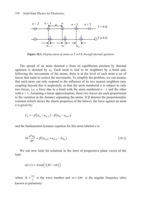
338 Solid-State Physics for Electronics
Figure 10.1. Displacement of atoms at T 0 K through thermal agitation
The spread of an atom denoted n from its equilibrium position by thermal agitation is denoted by un. Each atom is tied to its neighbors by a bond and, following the movements of the atoms, there is at the level of each atom a set of forces that tends to correct the movements. To simplify the problem, we can assume that each atom can only respond to the influence of its two nearest neighbors (any coupling beyond this is neglected), so that the atom numbered n is subject to only two forces, i.e. a force due to a bond with the atom numbered n - 1 and the other with n + 1. Assuming a linear approximation, these two forces are each proportional to the variation in the distance separating the atoms. If denotes the proportionality constant (which shows the elastic properties of the lattice), the force against an atom n is given by:
1 1n n n n nF u u u u
and the fundamental dynamic equation for this atom labeled n is:
1 1²
2²n
n n nd u
M u u udt
[10.1]
We can now look for solutions in the form of progressive plane waves of the type:
( , ) expu r t A i Kr t
where 2K is the wave number and 2 is the angular frequency (also
known as pulsation).
n 2 n 1 n n + 2n + 1 T = 0 K
T 0 K
un 1 un un+ 1
a

The Principal of Quasi-Particles 339
This means looking for the solution for the movement of the atom n located by r = na, and such that ( , ) expnu na t A i Kna t . Similarly, we also look for:
1 exp 1nu A i K n a t
and:
1 exp 1nu A i K n a t .
Substituting this into equation [10.1] we obtain:
² 2 2 cos 1iKa iKaM e e Ka ,
so that, using 2sin ² 1 cos 2x x , we find:
2 sin2
KaM
[10.2]
This is a dispersion equation based on ( )f K , and is periodic with respect to
K with a period given by 2a
as:
2( ) 2 sin ( ) 2 sin2 2
Ka KaK K
M a M
The representation is given in Figure 10.2a. However, given the periodicity it suffices in fact to represent the function (K) in an interval equal to 2
a which is
chosen to be between a
and a
(Figure 10.2b). The width of the first Brillouin
zone contains non-equivalent K values (the positive and negative values represent the two opposite directions in which the wave can move). This can be compared with the results in the following section.

340 Solid-State Physics for Electronics
Figure 10.2. (a) Dispersion curve [ (K)] for a chain of atoms;
and (b) representation for the first Brillouin zone
10.2.2.2. System properties
– Variations in the useful K zone. We have 1unun
iKa ie e . When Ka =
between and + , Ka takes n all possible independent values that give the dephasing ( ) in the movement of two neighboring atoms. For example, if two atoms are out of phase by
10x (with 0 10x ) it is the same as stating that
they are dephased by 1010
x . The range of variation in K is thus a a
K .
– Difference with the continuous medium (where a 0), and number of modes for a long chain. For the difference in a continuous medium where a 0, such that K (as maxK a ), with the example of a discrete chain of atoms, the
extreme values of K are max aK . For a progressive wave solution, such that in
terms of r we would have ( , ) expu r t A i Kr t , the use of the condition of
periodic limits u(r) = u(r + L) results in (see also section 2.4) 2LnK K n , where
n = 0, 1, 2.... Here the quantification is located at n as N represents the number of atoms in the chain such that L = Na. These values are the permitted values for K in the expression for the progressive wave u(r,t) solution for the system. The spectrum given by = f(K) is therefore discrete (see Figure 10.2b) and the interval denoted
K between two successive K values is simply 2L
K , such that with the width
of the Brillouin zone being given by 2aBrilK , K can take on
22
a LL a
N values.
K
2a
2
2a
2a
a
a
0
(a)
K
(K)
a
a 0
M 2M
2L
4L
6L
sv K
(b)
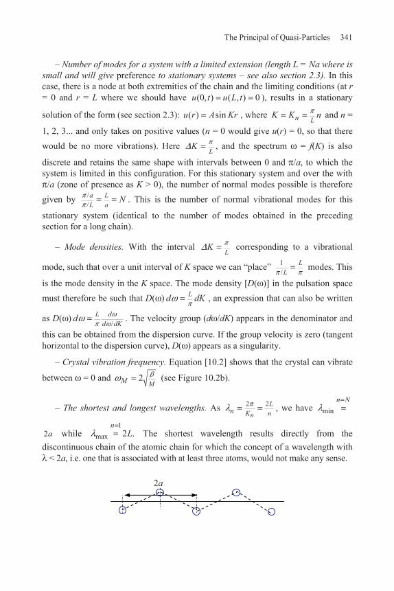
The Principal of Quasi-Particles 341
– Number of modes for a system with a limited extension (length L = Na where is small and will give preference to stationary systems – see also section 2.3). In this case, there is a node at both extremities of the chain and the limiting conditions (at r = 0 and r = L where we should have (0, ) ( , ) 0u t u L t ), results in a stationary
solution of the form (see section 2.3): ( ) sinu r A Kr , where LnK K n and n =
1, 2, 3... and only takes on positive values (n = 0 would give u(r) = 0, so that there would be no more vibrations). Here
LK , and the spectrum = f(K) is also
discrete and retains the same shape with intervals between 0 and /a, to which the system is limited in this configuration. For this stationary system and over the with
/a (zone of presence as K > 0), the number of normal modes possible is therefore given by /
/a LL a
N . This is the number of normal vibrational modes for this
stationary system (identical to the number of modes obtained in the preceding section for a long chain).
– Mode densities. With the interval L
K corresponding to a vibrational
mode, such that over a unit interval of K space we can “place” 1/
LL
modes. This
is the mode density in the K space. The mode density [D( )] in the pulsation space must therefore be such that D( ) Ld dK , an expression that can also be written
as D( )/
L dd dK
d . The velocity group (d /dK) appears in the denominator and
this can be obtained from the dispersion curve. If the group velocity is zero (tangent horizontal to the dispersion curve), D( ) appears as a singularity.
– Crystal vibration frequency. Equation [10.2] shows that the crystal can vibrate
between = 0 and 2MM (see Figure 10.2b).
– The shortest and longest wavelengths. As 2 2LK nnn , we have min
n N
2a while 1
max 2 .n
L The shortest wavelength results directly from the discontinuous chain of the atomic chain for which the concept of a wavelength with
< 2a, i.e. one that is associated with at least three atoms, would not make any sense.
2a

342 Solid-State Physics for Electronics
– Propagation velocity and wave frequency. For a small value of K (equivalent to having large wavelengths corresponding to acoustics vibrational modes), an approximation can be made as in
2 2sin Ka Ka . Equation [10.2] then becomes linear,
as in M sa K v K and we have the straight line = vs |K| from Figure
10.2b. We thus find a remarkable property in that K sv v d
dK gv . Thus the
phase velocity and the group velocity have the same value, both equal to vs or rather the velocity of sound in solids (of the order of 105 cm s-1). This can be compared with the figure above and section 7.2.1 of [MOL 07b].
Thus setting sv a M , expression [10.2] can be written as:
2 sin2
sv Kaa
[10.3]
For ,a
k we have:
2 2
2 cos 02 2g kak
a
d a kav
dk M
The dispersion curve gives rise to a horizontal tangent with respect to a
k
(see Figure 10.2b). The wave at this point is stationary with a maximum angular frequency (pulsation) (see Figure 10.2) with a value deduced from equation [10.3] equal to max 2 vs
a. With vs 105 cm s-1 and a 10 8 cm, we find that max =
max/2 1013 Hz, which is in the infrared region.
K
slope vS

The Principal of Quasi-Particles 343
10.2.3. Oscillations within a diatomic and 1D chain
This section considers a chain made up of two types of atoms with masses m and M (M > m), each regularly spaced by a distance denoted a. The atoms with mass m are assumed to be placed at every 2na and those of mass M are at (2na a) = (2n 1)a, as shown in Figure 10.3.
Figure 10.3. Diatomic chain
Supposing that each atom interacts, once again, only with its closest two neighbors, and that the interaction constants ( ) are identical between paired neighbors, the equations for movement can be written as:
22
2 1 2 1 22
22 1
2 2 2 2 12
for atoms of mass , then 2
for atoms of mass , then 2
nn n n
nn n n
d um m u u u
dt
d uM M u u u
dt
[10.4]
Once again we are looking for solutions in the form of progressive waves, but with amplitudes and frequencies different for each type of atom (as their mass is different):
2 1
2 1 2
exp 2
exp 2 1n
n
u A j t Kna
u B j t n Ka [10.5]
Given the form of these solution, we thus have:
2 2 2 exp 2n nu u jKa and 2 1 2 1 exp 2n nu u jKa
a a
m M M M m m m
2n 2n 1 2n+1

344 Solid-State Physics for Electronics
On introducing [10.5] into [10.4] we find that:
21 2 2 1 2 1 exp 2 2n n nm u jKa u u [10.6]
22 2 1 2 2 1 1 exp 2 2n n nm u jKa u u [10.7]
From equation [10.7] we can pull out that:
2 1 222
1 exp 2
2n n
jKau u
M [10.8]
Equation [10.8] must be true for all values of time (t). According to [10.5], u2n varies with 1 and u2n+1 as a function of 2. We must therefore find that 1 = 2 = .
Inserting equation [10.8] into [10.6], we find that:
2 ² 2 ² 4 ² cos ² 0M m Ka
From this we deduce that:
4 2 ² sin ²2 4 0M m KaMm mM
[10.9]
This equation has two solutions for ² which can be denoted 2 and 2 and are such that:
22
4 sin ²1m M mM KamM m M
[10.10]
so that also:
22 1 1 1 1 4sin ²Ka
m M m M mM [10.11]

The Principal of Quasi-Particles 345
Figure 10.4. Acoustic and optical branches, with M > m
This result (equation [10.11]) shows that for a chain made up of atoms of varying nature there can be two types of vibrations with different frequencies, namely + and . In other terms, a value for K can correspond to two values for , and therefore two vibrational modes.
The solution + (upper branch of Figure 10.4) shows the optical branch of the
vibrational spectrum, whereas the solution (lower branch of Figure 10.4) is associated with the acoustic domain (low frequencies).
NOTE 1.– Using 2sin ² 1 cos 2Ka Ka , equation [10.11] can be rewritten as:
22 2 1 cos 21 1 1 1 Ka
m M m M mM
– When Ka is small we have cos 2 1Ka , and 1 12 2 ,m M
so that with
1 1 1μ m M
(reduced mass) then 2 .
Still in the condition of Ka being small, we have 0
0K
.
K
(K)
2a
2a 0
2 M
(b) acoustic
branch
2 m
Forbidden band
+ Optical branch
2μ

346 Solid-State Physics for Electronics
– When 2a
K , such that 2
Ka which gives cos 2 cosKa 1 ,
we have:
22
2
1 1 1 1 4
1 1 1 1
m M m M mM
m M m M
from which 2m
and 2 .M
NOTE 2.
– In the acoustic branch with modes for very low frequencies (K 0 and 0), equation [10.8] shows that u2n+1 u2n. This means that the atoms and the centers of their mass vibrate together (identical direction) and there is a translation of the complete cell, as shown in the top half of the figure above.
– For the optical branch, and when K 0, using 1 12 2m M
in equation
[10.8] we find that:
1 12 1
2
2
2 2m M
n
n
u mu MM
and the atoms vibrate with respect to one another but with the center of their mass fixed, as shown in the bottom part of the figure above.
NOTE 3.
– If two atoms carry opposing charges, we can imagine generate a vibration of this type using the electric field of a light wave – hence the name optical branch.
– Vibrations in the acoustic branch are tied to thermal effects and the passing of sound.
m M M m
m M M m

The Principal of Quasi-Particles 347
10.2.4. Vibrations of a 3D crystal
– Transverse and longitudinal modes. In 3D, the wave vector becomes 3D and the vector gives three corresponding vibrational modes. In addition to the longitudinal mode of the preceding section, there are also two transverse modes polarized at 90 to each other (for a definition of the various mode types see, for example, section 6.2 of [MOL 07b]). These two new transverse modes are also characterized by the curve (K) carrying acoustic and optical branches and a forbidden band.
Figure 10.5. Vibrational modes for a chain of atoms in
a 3D lattice: (a) longitudinal modes; and (b) transverse mode
– Number of modes. If the whole crystal encloses N atoms, then we have in all 3N vibrational modes with 2N of those being due to transverse vibrations and the other N being longitudinal (see problem 10.6.1).
– If the lattice contains two types of atoms (section 10.2.3), and taking into account note 2 of the preceding section, for the transverse modes and along the acoustic branch the two types of atoms oscillate in phase. However, along the optical branch, they vibrate in a mutually opposing phase.
Figure 10.6. Transverse modes for a lattice made up of two types of atoms: (a) acoustic branch; and (b) optical branch
x
y z
z
x
y x
y z
u
u
u
K
K
(a) (b)
M M
mm
mM
Mm

348 Solid-State Physics for Electronics
10.2.5. Energy of a vibrational mode
Here we use Debye’s theory where it is supposed that:
– Atomic oscillations in a lattice resemble a harmonic oscillator. The 3N vibrational modes are assumed to correspond to the same number of harmonic oscillators which have energy levels that are quantified by:
012nE E n , n = 0, 1, 2...
(see a course on quantum mechanics). The proper frequencies of the oscillator are equally spaced by an interval of 0. In Debye’s model, we can simplify the relatively complicated dispersion curve (and given by equations [10.2] or [10.11] for example) by considering the right-hand side, = vs|K|, no longer with the terms Kmax = a
, but rather with just Km being the total number of unnumbered modes equal
to 3N. Thus the Kn values of K are regularly spaced, the dispersion curve straightened, and the corresponding values for n are also regularly separated by
0Debyenotation
, just as in a harmonic oscillator.
– Oscillators are energetically distributed according to Boltzmann statistics. This indicates that the probability that a particular mode will have an energy En is proportional to exp En
kT.
So, at thermal equilibrium, the average energy for a pulsation mode given by
0 = is written as:
1 12 2
12
0
0
exp
exp
n n
n
n
n
kT
E
kT
[10.12]

The Principal of Quasi-Particles 349
By making kT
x , we obtain:
1 3
2 2
/2 3 /2
/2 3 /2
/2 2
/2
...
...
Ln 1 ...
1Ln
1
1 1 1Ln 1
2 2 exp / 1
x x
x x
x x x
x
x
x
e eE
e e
de e e
dx
de
dx e
dx e
dx kT
[10.13]
If T = 0K, then 120T K
E and this is the energy of what are generally
called the lattice zero vibrations. They are normally ignored when studying the thermal properties of crystals. In this approximation, we can therefore write from equation [10.13] that:
exp / 1E
kT [10.14]
NOTE.– The vibrational modes where ,kT with kT 0.026 eV at T = 300 K (i.e. acoustic modes with low energies and long wavelengths) have, according to equation [10.14], an average energy given by:
acoustic .1 1
kT
AE E kT [10.15]
When these conditions are present, the mode is termed as being completely excited. If T is sufficiently high so that this can be spread to 3N modes, the internal vibrational energy of the crystal is equal to 3NkT.

350 Solid-State Physics for Electronics
10.2.6. Phonons
10.2.6.1. Definition
Charge carriers (electrons, holes) continuously interact with the lattice, and give or gain energy from it. These exchanges of energy operate through transitions in vibrational modes. As the energy of each vibrational mode is quantified, the exchanges can only be quantified between energy levels of the form
1/ 2nE n . The transitions are in accordance with the selection rule n = 1, and the carrier–lattice interactions occur through absorption or emission
(generation) of quanta of energy. By analogy with photons, these quanta are termed phonons and they too can lead
a double life by exhibiting both wave and particulate natures. They are characterized by having:
– energy pnE
– quantity of movement K
– zero mass, like a photon
– and an absence of spin – such that the statistical form used to study them is that of Bose-Einstein (see equation [10.14] in which there is the Bose-Einstein
occupation factor given as 1exp / 1kT ).
10.2.6.2. Properties of phonons and the physical role of semiconductors
Each normal pulsation ( ) contains n phonons of energy . This energy is, in reality, a pretty small amount. As we saw above, even when fully excited (in the acoustic mode), then kT 0.026 eV. However, the amount of movement can
actually be quite high, as K can reach a
which is of the order of the quantity of
movement of electrons in the Brillouin zone.
E
r r0
n = 0 n = 2
n = 1 E0
E3 n = 3
Figure 10.7a. Levels in a harmonic oscillator

The Principal of Quasi-Particles 351
The electron-lattice vibration interaction can therefore be thought of as the interaction of two bodies, namely electrons and phonons with a conservation of energy and a quantity of movement.
Given a phonon’s characteristics, a collision between an electron and a phonon
can little change the energy of the electron but may greatly change its quantity of movement. This is the mechanism used in transitions between permitted bands in indirect gap semiconductors (from the extrema of valence and conduction bands obtained for wave vector different values, i.e. ki and kf as shown in Figure 10.7b). The variation in energy is assured by the photon that produces the vertical transition (i.e. without change in quantity of movement) and the phonon that gives the quantity of movement, as in i fk k which makes an oblique transition possible.
Numerically, the wave vector for the photon is given by ptk3
2 10 nm
2 110 nm , while that of the phonon is better written as 0.3 110
a
a nmpnK nm .
10.2.7. Conclusion
To resume, it is possible to represent, indifferently, the vibratory states of a crystal:
– either as a sum of 3N vibrational modes of which the average energy for a pulsation mode (otherwise known as the angular frequency and denoted ) is given by
exp / 1kTE ;
– or as a free “phonon gas” in which the quasi-particles exhibit their double character of wave or particle with a low energy and a high degree of movement.
Figure 10.7b. Indirect (oblique) transition causing introduction of a phonon
E
k
phonon o
BC
BV
kf ki
h photon

352 Solid-State Physics for Electronics
It is also possible to state that, in contrast to electrons, the number of phonons for a given energy state is not limited. There is a constant annihilation and creation of phonons in the lattice. The conservation of the number of phonons present is not obligatory.
10.3. Polarons
10.3.1. Introduction: definition and origin
Simplistically put, we can think of electrons or holes moving in a crystal. Due to the charges they carry, they displace the ions, which are of opposite charge, in the lattice and can even create a polarization associated with the resulting deformation. This force for such a change is occasionally called a constraining field. The charged particle (electron or hole) and the associated deformation (by polarization) form the so-called polaron quasi-particle. As the charged particle moves in the crystal, it “pulls” on the deformation increases its effective mass and correlatively decrease its mobility (see section 8.1.3).
The polaron can be thought of as an electron-lattice coupling, as it is the latter
that provokes, in some senses at least, the localization of the charge into the deformation where it represents a reduced mobility with respect to a configuration where the deformation of the lattice would be inexistent or negligible. The latter case happens in covalent crystals as these are made up of neutral atoms which have weak interactions with the charges (electrons or holes). The effects are considerably greater in ionic crystals because of the strong Coulombic interaction between charges and ions.
The pairing can also be thought of as an electron-phonon coupling, where it is
the longitudinal phonons that stimulate deformations and with them propagate with the charges. This is a mechanism that would explain the transport of polarons. In the case of non-polar solids, the dominant interaction is with acoustic longitudinal polarons. However, in polar media, it is the optical longitudinal polarons that are strongly coupled with electrons. This is due to great variations in the active dipolar moments associated with atomic displacements in opposition to the phases induced by optical phonon modes (see also note 2 in section 10.2.3).
10.3.2. The various polarons
10.3.2.1. Dielectric polarons
If we take an ionic crystal lattice, as shown in Figure 10.8a, and then place an electron on an ion, as detailed by the black point in Figure 10.8b, then we can see

The Principal of Quasi-Particles 353
that surrounding ions undergo a force due to the additional electron. This electron–lattice interaction results in new positions for the ions, as shown in the same figure by dotted lines. This displacement of ions always results in a reduction of the energy of the electron, and also results in a potential well within which can be found the electron. If the well is deep enough then the electron will find itself in a tied state, incapable of moving to another site unless there is modification in the positions of neighboring ions. We can label the electron “self-trapped” and as such, it and its associated lattice deformation is termed a “polaron” The term originated from phenomena observed in polar materials; however, such quasi-particles can also occur in covalent materials.
Figure 10.8. (a) Lattice of ions in relaxed state; (b) repositioning of ions in directions of arrows following placement of electron at E in the lattice; (c) and (d) polaron formation in covalent materials going from a regular arrangement of rare gas atoms in (c) to a deformed atomic lattice after a hole has been placed at D.
10.3.2.2. Molecular polarons
Molecular polarons form in covalent materials in which the resulting distortion is confined to neighboring atoms, which can subsequently form a chemical bond while the charge is trapped. A good example is of Vk centers in alkali metal-halogen crystals, in which a hole trapped on a Cl ion results in attracting a neighboring Cl ion to yield a “molecular ion” of form Cl2 . Similar phenomena can occur in solid rare gases in which there is a trapped hole, as detailed in Figures 10.8c and d, and similarly in certain mineral glasses in which dangling bonds at a neutral site (D0) can result in a more favorable local rearrangement such that 2 D0 D+ + D- where D+
(a)
(c) (d)
D
E
E
(b)

354 Solid-State Physics for Electronics
and D- are the previously neutral dangling bonds (D0) that have, respectively, lost or gained an electronic charge.
Section 10.3.4 will detail the origin of polarons in molecular crystals (using the
Holstein model).
10.3.2.3. Small and large polarons
If the wavefunction associated with a self-trapped electron takes up a space equal to or smaller than the lattice constant, then the polaron is called a “small polaron” and the deformation is localized only in the neighborhood of the charge carrier. This type of quasi-particle is formed in covalent materials as they are essentially made up of neutral atoms which undergo only weak interactions with the charges (electrons or holes). The dielectric polaron can itself result in a small polaron when the distortion of the lattice is limited to the immediate neighborhood of the charge (as in Figure 10.8b). In the opposing case, then a large polaron, otherwise termed a “Fröhlich polaron”, can be formed in polar media in which Coulombic forces are involved that polarize the crystal over long distances (such as in metallic oxides). Small and large dielectric polarons are distinguished by a determination of the Fröhlich polaron coupling constant.
10.3.3. Dielectric polarons
Figure 10.9. Energy levels for an electron introduced in: (a) an isolated atom; (b) a solid wherein it delocalizes;
and (c) in a polar lattice where is becomes localized
If an electron is introduced into an unfilled orbital of a given atom in a solid, this electron can display one of two types of behavior, depending on the nature of the solid. They are:
– either the electron delocalizes into the bands resulting from an overlap of the orbitals of the atoms in the solid, and the electron is stabilized in the solid due to a
(a) introduction of an electron on an isolated
atom
(c) polarized lattice with the localization of the
electron (polaronic state) (b) solid state, with delocalization in a band of width B
B B/2
Ei

The Principal of Quasi-Particles 355
decrease in its energy by an amount that is of the order of B/2, where B represents the width of the permitted band (as in Figure 10.9a);
– or the electron will polarize the crystal, if the crystal will allow it, and there will be a displacement of neighboring atoms resulting in a deformation by polarization of the lattice. If it is assumed that the each electronic charge, denoted e, is spread around a spherical orbital with a radius r (associated with the assumed deformation of the lattice) then the energy of the charged sphere (assumed to be in equilibrium) can be written as 1 ²
2eCpE . Here, C is the capacitance of the sphere
and is given by 04 rC r where r is the relative permittivity. The change in the energy of the polarization by the charge in going from vacuum (localized on a single atom surrounded by a vacuum) to solid states, where the solid has a relative permittivity r, is given by:
2 2
solid vacuum0 0lattice
2
0
1 12 4 2 4
1 18
por
r
e eE E E
r r r r
er r
[10.16]
If we assume that the lattice deformation is only produced by the ionic and electronic polarizations, then the permittivity can be limited to the ionic and electronic components, as in ion optr , where opt , the electronic component
only appears in the optical domain (see section 3.4 of [MOL 07a]). r is the resulting permittivity which accounts for the establishment of the various polarizations (which a priori takes an infinite time) or zero frequency if r is static permittivity.
The decrease in electronic polarization energy is thus given by substituting opt
for r in [10.16], as in:
0
² 118e
opt
eE
r r [10.17]

356 Solid-State Physics for Electronics
With po e iE E E , the decrease in energy ( Ei) by the single ionic
polarization is given by:
0 0
0
² 1 ² 11 18 8
² 1 1 8
ir opt
opt r
e eE
r r r r
er r
[10.18]
Returning to Figure 10.8, it is possible to see that if Ei > B/2, the localized state (polaronic) is more stable than that that the electron would use. This condition can be seen as a proviso for the formation of a polaron. In this polaronic state, where the electron is spread over a radius r, its kinetic energy resembles that which it would have were it in a potential sphere of radius r such that
22 2 2 2
kin 2 2 22
2 * 2 *2 * 2
k h hE
m r m rm
(the effective mass accounts for the fact that the electron is tied to the lattice and is therefore not free).
The total energy of an electron localized in the sphere is thus the sum of this
kinetic energy and the energy gained through lattice deformation (ionic polarization). By deriving the energy with respect to r, and by making it equal to zero, we can work out the value of r that gives a stable state:
0
opt
8 ²* ² 1/ 1/ r
hr
m e [10.19]
A small value of r is favored by a large effective mass and a strong ionic polarization (that makes [ r – opt] large). In this case, and especially when m* is large, with have a narrow band system with a low mobility. Finally, if r < a (the lattice repeat unit) it can be said that we have a small polaron, however, if r > a, then it is called a large polaron.

The Principal of Quasi-Particles 357
10.3.4. Polarons in molecular crystals
10.3.4.1. Holstein’s model in equations
Molecular crystals can be used to obtain a simple, generalized model for small polarons (as with Holstein’s model in “Studies of polaron motion: Part I. The molecular-crystal model”, Annals of Physics, 1959, 8, 325). Just one excess electronis placed in a regularly aligned, flexible lattice of molecules (mass M). With each molecule denoted g we associate a coordinate xg that represents the movement of the molecule under a harmonic vibration of pulsation 0 with frequency:
Mk
21
0
Starting with a single molecular site and excluding coupling effects with surrounding molecules, (r) represents the potential energy of an oscillator and the vibrational force is given by )r( grad - )r(F . When r0 is in an equilibrium position, such that xg = r = r – r0 represents the local deformation of a molecule, we have (see section 10.2.1),
W(r) = W(r0) + 1
2 kxg² ,
where k is in accordance with the harmonic equation F(r) = M ²dtx²d g = kxg. The
solution, xg = X cos 0t, necessitates the introduction of an actual pulsation
0k
M
, and finally we obtain (with k = M 20 ):
W(r) = W(r0) + 21 M 2
g20x
Then 0 can be estimated for an elongation (xg) around about the same size as the
lattice constant (a) because the vibrational energy given by 21 M ²a2
0 is of the same
order as that of a bond energy (EL) in the molecule and EL 1 eV. With a 1 Å and M
= N
310 (hydrogen atom mass 10-3 kg), we have 20
2223
3 )10(
10x02.610.
21
= 1.6 ×
10-19 J and thus 0 1014 rad s-1. If a = 1 nm though, we now have 0 1013 rad s-1 and therefore, for heavier atoms, the frequencies are even lower.

358 Solid-State Physics for Electronics
On taking into account the coupling between the vibrational movement of a molecule and that of its neighbors, resulting in the transfer of vibrational energy throughout the lattice, we have to bring the phenomenon of frequency dispersion into play: = f(k). The Hamiltonian corresponding to the molecular crystal, without free charges, is written:
2 20 g
L 0 b g g h2g hg
M x² ²H M x x }
2M 2x
where h is the nearest neighbor, M is the reduced mass and 6 b is the size of the band of the optical phonons.
When an additional excess electron is introduced into the lattice, the electron-
lattice interactions can be accounted for by considering the excess carrier energy at a site in the lattice. We accept that the energy is a linear function of movement within the lattice, and the greater the induced movement then the greater the absolute value of the electron-lattice energy and the more easily the charge is self-trapped. This trapping is actually greater than any coupling.
For a carrier localized on a site g, we can write g'
g'0g xg) - f(g' - E E , in which
f(g' g) is a weighting factor which carries electron-lattice interactions. Assuming interactions are over short distances, f(g' g) = A g' g, and the above equation changes to Eg = E0 A xg, where E0 is the energy of a non-distorted site, Eg is E0 = 0 plus a constant and A represents the electron-site coupling force, as in
E grad - 0 - xE - E
- Ag
0g . In general, we write Eg = E(xg) = Axg.
Thus in the scenario we are considering, molecular deformations induced by the
charge carrier are mostly localized around the carrier itself, and it is the presence of vibrational coupling between neighboring molecules that distribute distortion effects beyond the occupied site. Figure 10.10, otherwise known as an Emin representation, presents a scheme of the distance from equilibrium of diatomic molecules – represented by vertical lines – in a linear molecular crystal about a site with an electron (black dot).
The complete resolution of this problem will require the use of Hamiltonian
operators (He) for strongly bonded electrons in a crystal of covalently bonded molecules, which will add a Hamiltonian for vibrational energies (HL).

The Principal of Quasi-Particles 359
Figure 10.10. Scheme of equilibrium separation distances for diatomic molecules in a linear chain, in which an electron (black dot) is placed at the center of a molecule
10.3.4.2. Limiting case of a single molecular site: polarons and bipolarons
10.3.4.2.1. One electron
In this limited example, we will place one excess electron on a single site, the molecule of which undergoes a deformation x. The potential energy of the site can be expressed as:
E = M 20
² 2x + (E0 – A x) = B x² A x where E0 = 0 and B = 1
2M 2
0
E is optimized for a value x = x0 such that:
0x x
Ex
0, so that M 20 x0 – A = 2x0 B – A = 0 x0 = 2
0
A A
2BM
Following a deformation (x0) of the lattice through vibration and electron-lattice interactions, the energy of electron-lattice interactions is accordingly reduced by Ax0 ( Ax0 written algebraically). Nevertheless, the system undergoes a distortion associated with a vibrational energy equal to B x0
2 which is such that:
Vibrational energy of molecular site
Energy of electron- lattice interaction (electron-vibration coupling)
Energy when there is no distortion

360 Solid-State Physics for Electronics
B x02 = B 0
2A
xB
=12
Ax0.
Thus the energy of the system is decreased by Ep, where:
Ep = B x02 – A x0 = –
12
Ax0 = – A4B
= – 20
A²
2M
The various energies are shown in Figure 10.11.
Figure 10.11. Different energy terms with respect to lattice deformation by an excess electron
Ax x0 x
Bx² Bx0
2
x0 x
Bx² – Ax x0 Ep = Bx0
2 – Ax0 x = (–A²)/2M 0
2
(a) vibrational energy
(b) energy of electron-lattice-
interaction
(c) resulting energy
energy recovered from
system relaxation
energy due to distortion
stabilized
system with reduced energy
Ax0
x

The Principal of Quasi-Particles 361
Just as in polarized media, the formation of a polaron is favored by the distortion energy being less (in absolute terms exactly one half) than the energy recovered from the reduction in the electron–lattice interaction energy.
10.3.4.2.2. Two electrons: the bipolaron
It is possible to simply adapt the single site model to a situation where there are two electrons localized on a deformed molecule. The energy is now
E = M 20
x²
2 – 2A x + U = B x² – (2A + C) x + U0
On replacing A in the preceding section with 2A + C, the minimum E is now given by
1 20
2A Cx x
M and EBP =
2
020
2A C U
2M
Two electrons localized on a single deformation is called a bipolaron and it is stable if the energy required for its formation is less than twice the energy of two isolated polarons, i.e. when
2
020
2A C U
2M < 2
0
A²
M
The above relationship can be true when A and C are of the same sign and when U0 is not too high. The deformation x1 imposed by the two particles (here two electrons, but it could also be holes) can be advantageous in overcoming moderate Coulombic repulsions.
10.3.5. Energy spectrum of the small polaron in molecular solids
As we have just seen, an electron that distorts the molecule onto which it is placed reduces its energy –Ax0 = 2Ep. The vibrational energy of the deformed
Coulombic repulsion due to 2 electrons on the same site. We can suppose that U
varies following U = U0 – Cx, in which U0 is the repulsion at zero deformation.
virbrational energy
electron lattice coupling energy

362 Solid-State Physics for Electronics
molecule increases by B x02 = |Ep|, and results in an overall reduction in energy for
the system (equal to Ep) with respect to the energy of an electron in a rigid crystal of molecules where xg = 0.
Within the limits of the preceding calculation, in which we have ignored
vibrational dispersions due to coupling with non-existing neighboring molecules, it is possible to state that:
p 20
A²E
2M
(see Figure 10.12).
Figure 10.12. Energy scheme for the small polaron
If a small polaron (charge carrier and associated lattice deformation combined) can be equally situated at any other of the geometrical equivalents in a crystal, then we find that the actual states of the system are shared in a polaronic band as shown in Figure 10.12. Using a modified method of that used for strong bond approximations (equation [10.2] and the following equations from Chapter 8), we
bonding energy due to polaron formation with molecular deformation in presence of charge
Ep
polaronic band due to site equivalence
overlap integral for two wavefunctions denoting
system vibrational state for a charge at one or other of
two neighboring sites
Ek = 12 J exp (–S)
electronic resonance integral
electron energy level in undeformed crystal

The Principal of Quasi-Particles 363
can consider that the proper states of a small polaron in a cubic crystal display an energy in the form:
Ek = – 2 J exp (– S) [cos kx a + cos ky a + cos kz a] – Ep
where:
– 2 2 2x y zk k k k is the polaron wave vector, and a the lattice constant;
– J is the resonance integral between two “electronically coupled” neighbors and is in the form exp(– R) to account for the exponential form of the electron wavefunctions; and
– exp(–S) is an overlap factor associated with chain vibrations. It represents the superposition integral between two wavefunctions, which detail the vibrational state of the system when the charge carrier is on one or another of two adjacent sites in a crystal. In the limiting case of a rigid lattice, the vibrational wavefunction remains unchanged during charge transfer from one site to its neighbor, and the overlap factor is equal to 1. However, here where we are looking at a distortable lattice, then exp(–S) can be considered to relate the necessary overlapping of atomic sites between which the required tunnel effect can occur to allow a complete displacement of atomic site and charge and is accounted for by J.
In fact, the transfer of a polaron requires two tunneling effects. One is associated
with moving a charge between two neighboring sites (electron resonance integral), while the other is the movement of the deformation and any sites geometrically tied to the deformation. Exp(–S) is a factor of the same order as the atomic tunnelling effect as it assimilates atomic site transfers. As it is associated with the high mass of atoms, relative to the charge carriers, its value is extremely low. For a cubic crystal, the polaronic band size is Ek = 12 J exp (–S) and is extremely narrow, of a width
typically below that of vibrational energies, which are at least kT 10-4 eV at temperatures not too close to zero.
NOTE.– The displaced deformation is equivalent to an “exchange” in position for two neighboring sites as demonstrated in Figure 10.13. Evidently, it is not two actual atoms which change place but their position relative to the deformation propagated with a charge.
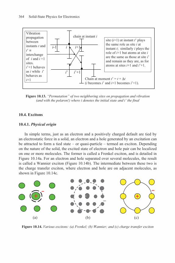
364 Solid-State Physics for Electronics
Figure 10.13. “Permutation” of two neighboring sites on propagation and vibration (and with the polaron!) where i denotes the initial state and i’ the final
10.4. Excitons
10.4.1. Physical origin
In simple terms, just as an electron and a positively charged default are tied by an electrostatic force in a solid, an electron and a hole generated by an excitation can be attracted to form a tied state – or quasi-particle – termed an exciton. Depending on the nature of the solid, the excited state of electron and hole pair can be localized on one or more molecules. The former is called a Frenkel exciton, and is detailed in Figure 10.14a. For an electron and hole separated over several molecules, the result is called a Wannier exciton (Figure 10.14b). The intermediate between these two is the charge transfer exciton, where electron and hole are on adjacent molecules, as shown in Figure 10.14c.
Figure 10.14. Various excitons: (a) Frenkel; (b) Wannier; and (c) charge transfer exciton
site (i+1) at instant t’ plays the same role as site i at instant t; similarly i plays the role of i+1 but atoms at site i are the same as those at site i’ and remain as they are, as for atoms at sites i+1 and i’+1.
chain at instant i
Chain at moment t’ = t + t (i becomes i’ and i+1 becomes i’+1).
i-1 i i+1
i’ i’+1
Vibration propagation between instants t and t’ interchange of i and i +1 sites. i’+1 behaves as i while i’ behaves as i+1
+
(a) (c) (b)
+

The Principal of Quasi-Particles 365
10.4.2. Wannier and charge transfer excitons
In solids such as semiconductors that have large permitted bands (B), electrons and holes exhibit high mobilities (μ) with μ being proportional to B (as detailed in band theory for covalent solids). Holes and electrons can easily separate, meaning low interaction energies.
Given that an electron and hole pair, with energy levels schematically illustrated
in Figure 10.16a are:
– buried within a continuous medium with permittivity given as = 0 r where r is relatively high for a reasonably well conducting medium (quite high mobility); and
– trace an orbit around one another in the material; thus this pair can be compared to the hydrogen atom where the nucleus is represented by the hole. The exciton is generally termed a Wannier exciton. With the energy levels quantified, and located with respect to the width of the gap of the material (EG) (see Figure 10.15), they are given by:
* 4ex
Gn G 2 2 2 20 r
m e 1E E
32 ² n
where *exm is the reduced effective mass of the electron-hole system and defined by
the expression * 1exm = * 1
em + mt*-1 where *
em and mt* are, respectively, the
effective masses of the electron and the hole. The dissociation of the exciton can be thought of as n and places the
electron and hole into free states with the electron in the conduction band. Their interaction energy is equal to zero but they are separated by an energy given by EG = EG . If the excitonic state corresponds to a given level denoted n, the electron and the hole are thus tied by a bonding energy Ebn such that
* 4ex
bn G Gn 2 2 2 20 r
m e 1E E E
32 ² n
In other words, this energy is what would be required to separate the electron and the hole from their bands where they are free (and such that n , Ebn 0).

366 Solid-State Physics for Electronics
With the energy of separation for an electron–hole pair in an exciton being given as EGn, the lowest frequency absorption corresponds to the energy transition EG1 rather than Eb1 (bonding energy).
Figure 10.15. The EGn energy level of an exciton with respect o the bonding energy level Ebn
The radius of the exciton (rn) can be evaluated using the electron–hole distance for a system based on hydrogen and is therefore written as rn = n² (4 0 rh²/m*e²). The distance r1 (n = 1) is the shortest as we have the lowest energy level for a Wannier exciton and thus the most bonded exciton state (like an 1 s-orbital). From the expressions for En and rn, we can see that bonding strength is essentially dependent on two parameters:
– the dielectric permittivity of the medium: the larger it is, the weaker the electron–hole attraction; and
– the reduced effective mass *( )exm for electron-hole pairs: the smaller it is, the greater the electron–hole distance (and by consequence the harder it is to retain the exciton).
Thus, for semiconductors which exhibit a large permitted band, high
permittivities and charge mobilities μ (with a low effective mass m* as, classically, μ = q /m*), only low bond energies appear (Wannier excitons). For semiconductors with an indirect gap, excitations of the lowest energy are forbidden as they require phonon intervention. For example, Wannier excitons have only been observed in semiconductors such as GaAs that have a direct gap.
Wannier excitons are theoretically possible for polymers. The bonding energy of
the exciton is of the order of 0.4 eV and exhibits an ellipsoid geometry. These values are representative of molecular excitons with a high degree of localization on a chain under strong electron–lattice interactions (and electronic and vibrational state
EG
exciton bonding energy Ebn
EG
O
energy
BV
BC
EG1 EGn

The Principal of Quasi-Particles 367
coupling). Polymers with a wide gap (insulators) must, nevertheless, present a weaker intra-chain delocalization and inter-chain interactions can be greater. In effect, charge transfer excitons (intermediate to Wannier and Frenkel excitons) are possible. The optimization of inter-chain contacts can result in excitons termed excimers (excitons shared over several identical molecular units) or exciplexes (excitons shared over two or more different molecular units).
Figure 10.16. Representations of excited states: (a) in a classic band scheme for semiconductors with a Wannier exciton; and
(b) in a molecular state with discrete levels for a Frenkel exciton
10.4.3. Frenkel excitons
In molecular crystals, the covalent bonds between atoms that make up the molecule are much stronger than intermolecular van der Waals bonds. Transitions between electronic levels of a practically isolated molecule in a dilute state and one in a condensed, solid state are only slightly changed in terms of frequency. Frenkel excitons are generally used to explain luminescence phenomena in molecular crystals through an excited state on a strongly bonded host molecule. The corresponding energy scheme is shown in Figure 10.16b.
Frenkel excitons are thus in a strong bond approximation with the excitation
localized on the same molecule or on an adjacent neighbor. They have been observed during – * transitions in aromatic molecules such as anthracene. Another example is that of excitations in ligand fields of d electrons, such as for nickel oxide.
While the particles that make up the electron-hole pair are bonded to one another
on the same lattice site, together they constitute a quasi-particle which can move through the crystal by transferring energy to neighboring sites. This representation of energy migration is confirmed by the fact that in crystals which contain

368 Solid-State Physics for Electronics
impurities, the excitations are trapped. It is in this manner that anthracene (which fluoresces on optical excitation), once doped with several parts per million of tetracene, sees its own fluorescence decrease and that of tetracene appear. This effect demonstrates that tetracene efficiently traps excitons, which can move across relatively large distances without relaxing. Given the relatively low concentrations of impurities, the distance covered can be of the order of a hundred molecules or more.
The movement of excitons can be due to overlapping of orbitals between
adjacent sites. However, it should be noted that during the permitted – * transitions, it is the electrostatic interaction tied to the dipolar momentum which gives rise to the greatest coupling energy between fundamental and excited states. This term is expressed in the form μij
2/R3 in which μij is the dipolar momentum for the transition between fundamental (i) and excited (j) states.
For adjacent molecules of different types, the excitation energy transfer mechanisms with long (dipolar interactions) and short (orbital overlapping) action radii will be detailed, along with Förster and Dexter transfers. These transfers help explain the interest in the use of optical doping of fluorescent molecules especially for organic LEDs and can also help get round selection rules to increase LED yields.
10.5. Plasmons
10.5.1. Basic definition
A plasma is a medium in which the concentrations of positive and negative charges are equal and at least one of the charges is mobile. In a solid, the negative conduction charges (electrons) have a concentration equal to that of the positive ions.
10.5.2. Dielectric response of an electronic gas: optical plasma
10.5.2.1. Dielectric function
To a first approximation, a solid contains a fixed number n of ions per unit volume with n free electrons that are placed in a vacuum. A good example of such a material could be an alkaline metal. The dielectric response of the electron gas to an electric field that is such that 00 e j t kzj t
x xE E e e E e is obtained by working out the integration of the fundamental dynamic equation. We can assume

The Principal of Quasi-Particles 369
that the electrons are not subject to recall or frictional forces. The equation, with respect to Ox is written as:
²²
d xm eEdt
From this equation, looking for forced solutions of the form 0j tx x e gives us
²eE
xm
The movement over a distance x by a charge (denoted -e) generates a moment dipole given by p ex , and the polarization (the dipole moment per unit volume) is therefore P = np. This means that
²²
neP Em
The dielectric function is such that 0 0() ( ) ( ) ( ) ( ),rD E E P so
0 0
²1 1²r
P neE m
With the plasma frequency being defined by ²
02 ne
mp , the dielectric function
can be written as:
21
²p
r
10.5.2.2. Optical plasma
The equation, ² ² ² rk c , for the dispersion of electromagnetic waves shows that there are two differing regions (see Figure 10.17). If:
– > p, r( ) > 0 and the wave number (k) is real, then the wave
0 e j t kzE E is progressive and the dispersion is given by 2 ² ²c kp .

370 Solid-State Physics for Electronics
– < p, r( ) < 0 and k is imaginary, as in k = jk '' then the wave E ''
0 0e j t kz k z j tE E e e is evanescent, i.e. it has no propagation term but just terms for oscillation and attenuation at the surface.
Figure 10.17. High band filtering characteristics of a plasma
In effect, the plasma behaves much as a high-band filter. As > p corresponds to < p, waves of lengths less than p can pass through the medium with '' = 0k , that is, without attenuation (without absorption). Alkaline metals where p 300 nm should therefore be transparent to wavelengths less than 300 nm, i.e. ultra-violet light.
Figure 10.18. Plasma dispersion curve
r( ) 1 0 0.5 1 1.5 / p
“drag” region propagation region < p vacuum vacuum > p
plasma plasma
> p
= c k
ck
p
> p
< p
r > 0 propagation
r < 0 evanescent wave
= 2 ² ²p c k

The Principal of Quasi-Particles 371
For 2 ² ²p c k , the transverse wave dispersion curve is shown in
Figure 10.18. The group velocity, = ddkgv , is the dispersion curve slope and is less
than the slope of the curve = ck , and hence lower than c.
10.5.2.3. Longitudinal optical modes in a plasma
The function ( ) is equal to zero at a frequency denoted L, so when
21 0
²L
L
pr ,
then also L p . A solution can arise for a longitudinal wave moving along x
(with a wave vector k ). For more details see a course of electromagnetism, also section 2.6.2, problem 6.
Therefore there is a mode of longitudinal oscillation for a gas of electrons in a
plasma. The angular frequency (or pulsation) L of these oscillations is in fact equal to the plasma pulsation p which in turn corresponds to the cutting frequency of the transverse electromagnetic waves.
Physically speaking, we can expect that a longitudinal oscillation of a plasma
through an elongation given by u will displace, for example, the electron gas upwards. The result of this negative charge in a section of width u is the formation of a layer with a surface charge given by = –neu (the charge found in a parallelepiped with a unit surface and a height u tending to zero). Similarly, at the bottom there is a surface layer with a charge = +neu. A field neu
0E is generated
inside the layer, which tends to push the electrons back to their equilibrium position.
Figure 10.19. Sections of a plasma placed in longitudinal oscillations with elongations denoted by u
++++++++++++++++++++++++++++++++++++++++++++++++++++++++++++
u
0
neuE

372 Solid-State Physics for Electronics
The field makes a recall force which is such that the dynamic fundamental equation relative to a unit volume of plasma can be written as:
0
² ² ²²
d u n e unm neE
dt
so that with 2
0
²p
nem
we have:
2² 0.² p
d u udt
This is the equation for a harmonic oscillator with an angular frequency p , otherwise called the plasma frequency. The same value of p is found via an alternate route in section 10.5.2.1.
10.5.3. Plasmons
10.5.3.1. Definition and generation
From what we have just seen, a plasma oscillation is a collective longitudinal oscillation of a conducting electron gas. By definition, the quantum energy p of
this collective plasma oscillation is called a plasmon, and ²
0
1/2.ne
mp
incident electrons
diffused electron (1 plasmon formed)
diffused electron (2 plasmons formed)
Figure 10.20. Generation of plasmons by electron diffusion

The Principal of Quasi-Particles 373
The pulsation, p, is of the order of 1016 rad s-1, and the energy of a plasmon in a wide range of solids can vary from around 3 to 30 eV. Simple thermal excitation of plasma oscillations is therefore impossible (kT 0.026 eV for T = 300 K). To excite plasmons it is necessary to, for example, have a flux of electrons penetrate the lattice. On moving to the interior of the crystal, each electron can excite several successive plasmons. Each plasmon is symbolized by .
10.5.3.2. Some properties
The high energies of plasmons can be explained by their oscillations being the result of a high number of electrons. The excitation of plasmons can be obtained either by making electrons (or ions or photons) traverse or reflect the film under study.
In a dielectric, it is also possible to excite collective plasma oscillations. Here it
is the valence electron cloud that as a whole oscillates with respect to the positive ions.
In semiconductors, two plasma oscillation modes can arise. One is at high
frequencies and involves all the valence electrons in an oscillation. The other, a low frequency oscillation, is associated with the electrons in the conduction band where
the plasma pulsation given by ²*0
1/2' ne
mrp is such that '
p ( 0.01 eV) is
small. At the interface between a metal and a dielectric (for example in the case of a
metal oxide layer on a metal) the surface plasmons can be excited and propagate with an energy that is less than those in the bulk. The study of surface plasmons makes it possible to gain information on the permittivity and thickness of the surface insulating layer.
10.6. Problems
10.6.1. Problem 1: enumeration of vibration modes (phonon modes)
This problem is based on a volume V of sides Lx, Ly and Lz belonging to a simple cubic system. It encloses N cubic elementary cells of sides a:
1) Determine the number of the vibrational modes.
2) Calculate the density of the vibration modes for each type of polarization by using the Debye approximation where = vs|K|.

374 Solid-State Physics for Electronics
Answers
1) For the cubic crystal (of sides Lx, Ly, Lz), the periodic limiting conditions
applied to the three components of the vector K gives x y zi K x K y K ze x y zi K x L K y L K z Le and hence the values 2
Lxx xK n , 2Lyy yK n ,
2Lzz zK n . The extremities of the K wave vectors are found at the nodes of an
orthorhombic lattice based on 2 /Lx, 2 /Ly, 2 /Lz. There are three nodes associated with each node (1L + 2T), and these three nodes give the elemental cell with a
volume given by 32 2 2 8
L L L Vx y z. The number (N3m) of these cells (associated with
three nodes) that can be placed in the first Brillouin zone with a volume of 2 3
a in
a cubic lattice is thus given by 3 32 8
3 ,Va V a
N where N is the number of cells
in the direct lattice, and hence also the number of atoms in the lattice (if on average there is one atom per crystal cubic cell). Definitely, we have N3m = N, and as N3m is the number of cell associated with three modes, then the total number of modes is 3N.
2) For a given polarization, we have a mode (with a given value of |K|)
associated with a cell of volume 32 2 2 8
L L L Vx y z. with a unit of reciprocal space,
there is therefore associated 13 38 / 8
V
Vmodes/polarization.
In addition, the mode density D(K) (where each is associated with a K value)
must be such that D(K)dK represents the number of modes characterized by a value of K between K and K+dK. These K values must therefore be found between the spheres of radius K and K + dK, i.e. within a volume 4 K²dK.
In this volume can be placed 4 ² ²3 2 ²8 /
1K dK K dK
V
Vcells for each mode (for a certain
polarization). We can set V = 1 so as to calculate the density. From this we find ²
2 ²( ) KD K .

The Principal of Quasi-Particles 375
As we should have D( )d = D(K)dK, we deduce that D( ) = D(K) dKd
, so that
with the Debye approximation where = vs|K| (and 1dKd vs
) we find
( )D ²32 ²vs
for the mode density for each type of polarization.
10.6.2. Problem 2: polaritons
In a 3D crystal there is a chain of ions separated by a distance denoted a. There are two types of ions; the positive and negative charges are alternatively placed. Ions with a charge +e and mass m are situated at z = 2na, while ions with the charge e and mass M are placed at z = (2n 1)a. Make a diagram of this.
The system is subjected to a transverse sinusoidal electric field xE Ox which
propagates along Oz. The equation for its form is xE 0 expE j t kz , where
the angular frequency is in the infra-red (IR) range, i.e. 1013 rd s-1.
1) Show that the IR wavelength is very large with respect to a ( 0.3 nm), and this makes it possible to neglect the propagation term in the expression for the IR wave. Write the new, approximate form of the equation, which will then be used in the following questions.
2) Taking only interactions between nearest neighboring ions, give the expression for the spread (A–B) in the distances between the two types of ions A and B. The result should be expressed as a function of the masses of the ions, their
charges and angular frequencies ( ) and 2μT , where is the coupling
constant between ions and μ is their reduced mass.
3) Give the general equation for the dipole moment with respect to x for a system based on two ions and their nearest neighbors. From this deduce the model for the ionic polarization vector in a solid containing N pairs of ions (of the type studied) per unit volume.
4)
a) Establish the expressions for the dielectric permittivity [ ( )] as a function of N, μ, , T, and .
b) Introduce the parameter ²2 Neμp into the equation for ( ) and from this
deduce the (Born) equation for the static permittivity [ (0)] which is such that (0) = s by notation. Finally, express ( ) as a function of s, , T, and .

376 Solid-State Physics for Electronics
5) Make 2 2 sL T (in the Lyddane-Sachs-Teller equation). Express ( ) as a
function of , T, L, and . From it deduce the physical significance of L, and then the domain of the angular frequency (otherwise called pulsation) for which the electric waves are reflected by the crystal.
6) Plot the curve ( ) = f( ). Study, in particular, the pole and the zero points of the dielectric function ( ). Show how the pulsation ( L) corresponds to a longitudinal mode wave. Detail the consequence of this.
7) Show that in an ionic crystal where both phonons (vibrational movements) and plane transverse electromagnetic waves in the IR region that the dispersion equation can be written as 4 2 2 2² ² ² ² 0r rs T Tk c k c . Note that the
IR wave is in the domain of the proper pulsation ( T = 2μ
) of transverse optical
phonons, and the index r of the permittivities designates that they are relative dielectric permittivities.
8) The quantum of fields coupled with photons (transverse electromagnetic waves, xE 0 expE j t kz ) and of transverse phonons is called a polariton.
Show graphically the dispersion curves for these fields that are initially uncoupled and then coupled.
Answers
1)
We have 2c c , so with 1013 rd s-1, we find that 200 μm. With a
0.3 nm it is possible to state that >> a. The wave remains practically constant over a large part of the z length of the chain – and makes it possible to neglect the term for the propagation. The form of the wave can thus be reduced, by neglecting the propagation term, to 0 exp .xE E j t Mathematically speaking, we can also say that as k = 2 / is very small especially when is becomes very large with respect
+ + + + + z
k
Ex
M, 2n - 1
m, 2n x

The Principal of Quasi-Particles 377
to z, the product kz tends towards zero, and therefore the term exp( ) exp 0 1jkz and Ex is reduced to:
0 0exp exp( ) expxE E j t jkz E j t
2) The movement equations are forced by the electric field to give:
– for atoms of mass m, we have
22
2 1 2 1 2 02 2 j tnn n n
d um u u u eE e
dt
– and for atoms of mass M, then
22 1
2 2 2 2 12 2 j tnn n n
d uM u u u eEe
dt
The search for forced solutions written as 2j t
nu Ae and 2 1j t
nu Be , substituted in to the preceding equations gives:
– 0² 2m A B A eE
– 0² 2M B A B eE By dividing the first equation by m and the second by M, then subtracting term
by term, we find that by making 1 1 1μ m M
and 22μT
(frequency of the branch
of optical phonons when K 0) that:
02 2T
eEA B
μ [10.20]
The equation that is thus obtained shows that there is a resonance frequency attained when = T (between the excitation of the pulsation wave and the optical phonons when K 0).

378 Solid-State Physics for Electronics
3) The negative and positive charged ions are therefore displaced in the opposite sense to the electric field and generate a dipole moment of an amplitude |me| = e(A – B). By definition, the polarization is the dipole moment per unit volume. If N represents the number of ion pairs (and hence dipoles) per unit volume, then the modulus of the ionic polarizability (associated with the displacement of only the ions) is Pion = N me (A – B), so that:
ion 02²
²T
NeP Eμ
[10.21]
4)
a) In general terms, 0 .P E The polarization P( ) of a given pulsation can be composed of two terms:
– one for the polarization which establishes itself instantaneously and is associated with the electronic polarization (where the electrons can instantaneously follow and applied field) and takes on a frequency = [1/(t 0)] = :
0P E ;
– and another (Pion) here associated with a slower ionic polarization that that above.
We therefore have:
0 0
ion 0 0 02²
²T
P E
NeP P E E
μ
b) With ²2 Neμp , and ²
02 Ne
μp where p is the plasma pulsation, we have:
2
2 2²( )
² ²p
T T
Ne
μ [10.22]

The Principal of Quasi-Particles 379
From equation [10.22] it is possible to deduce the Born equation, as in:
2notation
2(0) ps
T [10.23]
The result is 2 2p s T . Taking the last equation and placing it into
equation [10.22], we have:
2
2( )
²T
sT
[10.24]
5) Here we make:
2 2 sL T [10.25]
In passing, we can write equation [10.25] in another form, i.e.:
2
2T
s L [10.26]
and it is this that makes up the so-called Lyddane-Sachs-Teller equation and in which we can determine the physical significance of L.
To make equation [10.25] appear in [10.24] we can write:
2 2
2 22 2
2 2 2 2
2 2
( ) 1 T Ts
TT
T T T s
T

380 Solid-State Physics for Electronics
So that with equation [10.25]:
2 2
2 2L
T [10.27]
And then we see straight away that 0L
.
As s > , then according to equation [10.25] L > T. The result is that when
T < < L, we have ( ) < 0. In this case, the relation for the dispersion of transverse electromagnetic waves:
0
² ² ( )² ( )² ²rk
c c,
shows that when ( ) < 0, k² < 0, then ''k ik must be true and contains a pure imaginary number. The wave thus becomes:
0 exp[ '' ]exp[ ]xE E k r j t
and is retarded (evanescent) in the material and no longer propagates. This corresponds to a forbidden band for pulsation waves between T and L.
6) Especially when using equation [10.27] we can see that the limiting values are as follows:
– when = 0, we have ( ) = s;
– when , ( ) ;
– when T , ( ) + ;
– when T+, ( ) ;
– when = L, ( ) = ( L) = 0. From this it is possible to deduce the curve shown in the figure on the next page. The highest point for the dielectric function is at T (resonance frequency
between the IR wave and the transverse optical phonons). The zero point for this dielectric function is obtained when = L.

The Principal of Quasi-Particles 381
In general terms, the Gauss equation, div ( )div 0D E , has in fact two solutions:
– either div 0E (and hence ( ) 0, which happens when L), from which we deduce that . 0ik E . We therefore have E k which corresponds to a transverse wave structure;
– or ( ) = 0, which is the precise result when = L. In this case, the Gauss equation is true without the wave necessarily being transverse (as div 0E no longer has to be true). We can now go on to look for the form of the wave.
Here, as usual, we have:
div 0 . 0B ik B 0B
0 0rot 0 0LE
B μ j μ E ik Bt
The wave can therefore only be purely electrical. The Maxwell-Faraday equation makes it possible to state that rot 0,B
tE so that in addition, rotE j B 0. With
0,B we have rot 0,E and 0,jk E and hence .E k This means that E is directed along k and the wave has a longitudinal structure. Finally the pulsation denoted L appears either as the upper limit for the forbidden band, either as the pulsation with which is associated a longitudinal phonon.
s
T L
( )
0
forbidden band

382 Solid-State Physics for Electronics
7) Taking the equation for the wave dispersion, ² ² ( )² ² 0
² ( )c crk , the
expression given in [10.27] can be written dividing through the members with 0, as
in 2 2
2 2L
Tr r . We obtain: 2 2² ² ² ² ² ² ²T r Lk c k c , such that
4 2 2 2² ² ² ² 0r r L Tk c k c . Using the Lyddane-Sachs-Teller
equation, i.e. 2 2r L rs T , we find:
4 2 2 2² ² ² ² 0r rs T Tk c k c [10.28]
8) The solutions for equation [10.28] are in the form:
22 2 2 21² ² ² ² 4 ² ²
2rs T rs T r T
r
k c k c k c [10.29]
In addition, the dispersion relation ²²
² ( )c rk associated with equation
[10.27] written in the form 2 2
2 2L
Tr r , shows that:
– when k 0, there are two possible solutions:
- either 0, which corresponds to the smallest obligatory solution for equation [10.29], as can also be directly verified by placing k 0 in to the equation for ,
- r( ) 0, which can be obtained when L. This is also in accordance with the LST equation in which
2 2sL T . This solution corresponds to the
solution + as can be directly verified in equation [10.29] when placing k 0 in +;
– when k , there are two further solutions:
- either c
and rck and hence the solution for +. The
introduction into equation [10.29] for k , such that k²c² >> 2rs T , where
k²c² >> 2r T and goes towards a solution for + as
r
ck ,

The Principal of Quasi-Particles 383
- or 2 2
2 2L
Tr r , which is obtained when T, and
corresponds for the solution for in equation [10.29].
The = f(k) plot shows two sets of curves associated with the transverse waves (set T) for two solutions + and . These are the coupled modes for photons and transverse optical photons in an ionic crystal containing the polaritons.
As shown in the figure above, these two solutions are separated by a forbidden zone (or band) with respect to the propagation of the electromagnetic waves:
the value = L corresponds to a longitudinal wave (L) and is the vibration of longitudinal optical phonons;
the value = T is for a transverse wave (T) and is the vibration of transverse optical phonons.
The dotted line represents the (straight) dispersion curve for single photons in a
crystal (uncoupled with the lattice vibrations). This coupling effect, that modifies the resonance frequencies (for photons with
angular frequencies with phonons with angular frequencies denoted T and L), the propagation property of the electromagnetic wave is therefore reflected when is such that T < < L.
In this zone, the electromagnetic wave vector is purely complex. This can be
considered as a breaking of the wave in the neighborhood of the surface of the solid.
T
r
ck
+
T
k
T
L
O
zone unavailable to propagation: reflection zoneL

This page intentionally left blank

Bibliography
[AND 58] ANDERSON P.W., “Absence of Diffusion in Certain Random Lattices”, Phys. Rev., 109, 5, p.1492–1505, 1958.
[ASH 76] ASHCROFT N.W and MERMIN D., Solid State Physics, Saunders College Publishing, 1976.
[BRO 92] BROUSSEAU M., Physique du solide, Masson, Paris, 1992.
[CAZ 96] CAZAUX J., Initiation à la physique du solide, Masson, Paris, 1996.
[FRI 70] FRITZSCHE H., “CFO Model”, la Recherche, Novermber, p. 527, 1970.
[GER 97] GERL M. and ISSI J.P., Physique des matériaux, Presses Polytechniques et Universitaires Romandes, Lausanne, 1997.
[IOF 60] IOFFE A.F., REGEL A.R. “Non crystalline, amorphous and liquid electronic semiconductors”, Progress in Semiconductors, vol. 4, Heywood and Co Ltd, London, 1960.
[KIT 63] KITTEL C. Quantum Theory of Solids, Wiley, New York, 1963.
[KIT 96] KITTEL C. Introduction to Solid State Physics, Wiley, New York, 1996.
[LEV 95] LEVY F., Physique et technologie des semi-conducteurs, Presses Polytechniques et Universitaires Romandes, Lausanne, 1995.
[MIL 60] MILLER A. and ABRAHAMS E., “Impurity Conduction at Low Concentrations”, Phys. Rev., 120, 3, p.754–755, 1960.
[MOL 06] MOLITON, A. Optoelectronics Of Molecules And Polymers, Springer, New York, 2006.
[MOL 07a] MOLITON A., Applied Electromagnetism and Materials, Springer, 2007.
[MOL 07b] MOLITON, A. Basic Electromagnetism and Materials, Springer, New York, 2007.
[MOO 93] MOOSER E., Introduction à la physique des solides, Presses Polytechniques et Universitaires Romandes, Lausanne, 1993.

386 Solid-State Physics for Electronics
[MOT 79] MOTT N.F. and DAVIS E.A., Electronic Processes in Non-crystalline Materials, Clarendon, 1979.
[QUE 88] QUERE Y., Physique des matériaux, Ellipses, Paris, 1988.
[SAP 90] SAPOVAL B. and HERMANN C., Physique des semi-conducteurs, Ellipses, Paris, 1990.
[SMI 67] SMITH R.A., Wave Mechanics of Crystalline Solids, Chapman & Hall, London, 1967.
[TEY 92] TEYSSIER J.L. and BRUNET H., Physique des matériaux conducteurs et semi-conducteurs, Dunod, Paris, 1992.
[VAP 70] VAPAILLE A., Physique des dispositifs à semi-conducteurs, tome 1 : électronique du silicium homogène, Masson, Paris, 1970.

Index
A alloys, 182, 183, 185 Anderson localization, 312, 315 anti-bonding, 206-210, 226, 237-242,
245-250 asymmetric well, 18, 23
B band structure, 187, 189 band summit, 9 band width, 255, 291 band, 1, 249, 282
conduction band, 12, 13, 18, 19, 24, 30, 31, 38, 187, 189, 194, 195
energy band, 70 forbidden band, 224, 226, 248, 347,
381, 382 valency band, 188, 189
Bloch, 55-59, 80-82, 85, 86 bonding levels, 242 bonding, 207, 208, 238, 239, 246 Bragg, 138-141 branch, acoustic branch, optic branch,
345-378 Brillouin, 123, 132, 135-138, 140,
142, 143, 145-162, 165-174
Brillouin zone, 138, 149-152, 157, 168, 173, 176, 187, 340, 341, 351, 375
C carbon diamond, 249, 258, 276, 301 centered cubic (cc), 175, 250, 256 central equation, 80, 82 CFO, 325 chain, 210, 211, 213, 215, 217, 224,
225, 227, 228, 230-234, 237, 239-242, 245, 247-249
conductivity, 310, 320-323, 326 copper, 173, 182, 185 Coulomb integral, 223 couplings (orbital), 218 covalent (crystal), 249, 258, 268,
269, 274, 278 CTCs (complex transfer charge), 310,
312
D Debye (approximation), 348, 374,
375 defects, 301, 324, 326 diamond, 249, 258 dielectric function, 369

388 Solid-State Physics for Electronics
dielectric polarons, 353, 354 diffraction, 129, 130, 134, 138, 140 diffusion, 128-141 direct gap, 190 direct lattice, 123, 134, 138, 139,
142, 144-149, 159, 161, 165, 168, 171-173
disorder, 302, 309, 312-316, 318, 320-326
dispersion curve, 220, 231, 250, 252, 294
dispersion, 339, 341, 342, 348, 358, 370, 371, 377, 381, 383, 384
distorted, 225, 227, 228, 231-234
E effective mass, 1, 187, 195, 196, 255,
257, 289, 297, 300 electronic density, 17, 44 Esaki, 31 Ewald, 135 excitons, 336, 365, 367-369 face centered cubic, (fcc) 173, 174,
178, 181, 182, 184, 186, 192, 194, 254, 256-258, 276, 280, 295, 298, 300, 301
F FBC, 19, 20, 29, 30-32 Fermi energy, 28, 44, 47 Fermi level, 18, 19, 38, 39, 42, 43,
47-49, 232 Fermi surface, 150, 151, 153, 154,
156, 163, 170 Fermi-Dirac, 15, 38, 40, 44 Floquet, 211-214, 217, 225, 246, 248 forbidden, 69, 72, 75, 76, 78 free electron, 1, 13, 17,20, 25, 29, 44,
49, 50 Frenkel (exciton), 365, 367, 368
G, H GaAs, 24, 25, 30, 31 heterostructure, 22, 23, 31 holes, 8, 10, 13, 15-17, 25, 31, 32 Hubbard, 302-304, 306, 307, 309,
326 Hückel, 213, 214, 218, 220, 223 Hume-Rothery rules, 183 hybridization, 249, 258-262, 266,
267, 269, 270, 272, 288
I index, 126, 138 indirect gap, 189, 190 insulator, 1, 11, 18, 21, 147, 156-158 Ioffe-Regel (conditions), 312, 313,
316, 318, 335 isolated, 306
L lattice
1D, 146, 147 199, 210, 211, 215, 225, 234, 242
2D lattice, 125 3D lattice, 142, 249, 275
Laue, 128, 133, 134 longitudinal wave, 372, 384 Lyddane-Sachs-Teller, 376, 380, 383
M Mathieu, 59, 61, 65, 70, 78 metal, 1, 18, 19, 21, 38, 147, 156-
158, 303-309, 320-323, 326, 331 Miller, 125-129, 138 mobility, 257, 314, 315, 321, 326,
333-335 mode density, 341, 375 Mott, 303, 305-307, 309-312, 315,
317, 318, 320, 325-327

Index 389
N nodes, 123-126, 128, 132, 134, 135,
137, 138, 164, 168
O orbitals
molecular orbitals, 199, 203, 208-210
p orbitals, 209 s orbitals, 200
oscillations, 337, 343 oscillator, 348, 357, 373 overlap, 12, 14, 15, 17, 18, 21
P PBC, 25, 30-32, 50 Peierls, 229, 231, 232, 240 phonons, 335, 336, 350-352, 358,
377, 378, 381, 384 plasma, 369-374, 379 plasmons, 336, 373, 374 polarons, 335, 352-354, 357, 359,
362 polymers, 311, 312, 333-335 potential box, 32 proper function, 57-59, 76 proper value, 279-281
Q quasi-particles, 335, 336, 352, 353
R reciprocal lattices, 123, 173 reduced zones, 20, 22, 142, 145, 150,
151, 161, 174, 175 relaxation, 228, 229, 233 resonance integral, 223, 249 reticular plane, 125, 138, 144
S semi-conductors, 17, 147, 156, 157,
163 semi-free electron, 56-59, 83, 137,
148, 151-153, 156, 159, 163-165 semi-Free, 1 semi-metal, 11, 12, 17, 21 silicon, 173, 186, 249 simple cubic, 124, 128, 142, 143,
148, 149, 154, 250-252, 255-257 state density, 12-14, 17, 19, 20, 38,
194, 195, 198, 229, 320, 329 stationary regime, 19, 23, 41 stationary wave, 73 superlattices, 1 symmetric well, 18, 19
T transition, 189, 351, 366, 369 transverse modes, 347
V vibration, 337, 338, 341, 347, 351,
357, 360, 364, 374, 384
W Wannier (exciton), 365, 367, 368 wave function, 199, 200, 203-208,
211-214, 216, 226, 234, 237, 239, 241-249, 258, 262, 267, 275, 276, 279, 286, 287, 305, 313-319
weak bond, 55, 71, 72 Wigner-Seitz, 125, 135
Z Z(E), 12, 13, 14, 17, 19, 18, 27, 28,
29, 30, 37, 38, 41, 42, 44, 46, 49, 50, 51, 53


