29
Slide: 1 ESLS-RF 04/10/2011 Solid state power amplifier development at ESRF M.Langlois

Slide: 1 ESLS-RF 04/10/2011
Solid state power amplifier development at ESRF
M.Langlois

Slide: 2 ESLS-RF 04/10/2011
Motivation
•Get some insight of the “do and don’t” of solid state amplifiers. •Adapt them better to synchrotron light source service.

Slide: 3 ESLS-RF 04/10/2011
Available RFpower components
Klystron MW range 3 acknowledged manufacturers
Thales TH 2089
IOT a few 10 kW 3 acknowledged manufacturers
LDMOS a few 100 W 2 acknowledged manufacturers
Transistors are fashionable because : •Few people accept to deal with high voltages
•Due to the so-called graceful degradation, they fit in the operation schedule of a light source

Slide: 4 ESLS-RF 04/10/2011
Cavities
ESRF Voltage: 1.6 MV TTC
Power: 300 kW at 200mA
ALBA Voltage: 600 kV TTC
Power: 140 kW at 400mA
SOLEIL Voltage: up to 5 MV TTC
Power: up to 400 kW

Slide: 5 Accelerator & Source Division Day
How to bridge the gap?
transistors cavities
Direct implementation
RF modules
Combining tree
cavity combining

Slide: 6 Accelerator & Source Division Day
RF module
Matching
circuit
Matching
circuit
Input balun
Output balun
circulator
Bias circuits

Slide: 7 Accelerator & Source Division Day
Cost : expensive parts
•Transistor •Circulator •Baluns •Choke • All components forbidding pick and place

Slide: 8 ESLS-RF 04/10/2011
Baluns
Balun transformer
Coaxial implementation

Slide: 9 Accelerator & Source Division Day
Planar printed baluns
Motorola patent
unbalanced
balanced
Balanced on top Unbalanced on bottom
NXP design
The cooling plate has to be milled and the balun is
difficult to cool

Slide: 10 Accelerator & Source Division Day
Design codes CST Microwave
Printed balun model
Printed balun, matching circuit and bias model
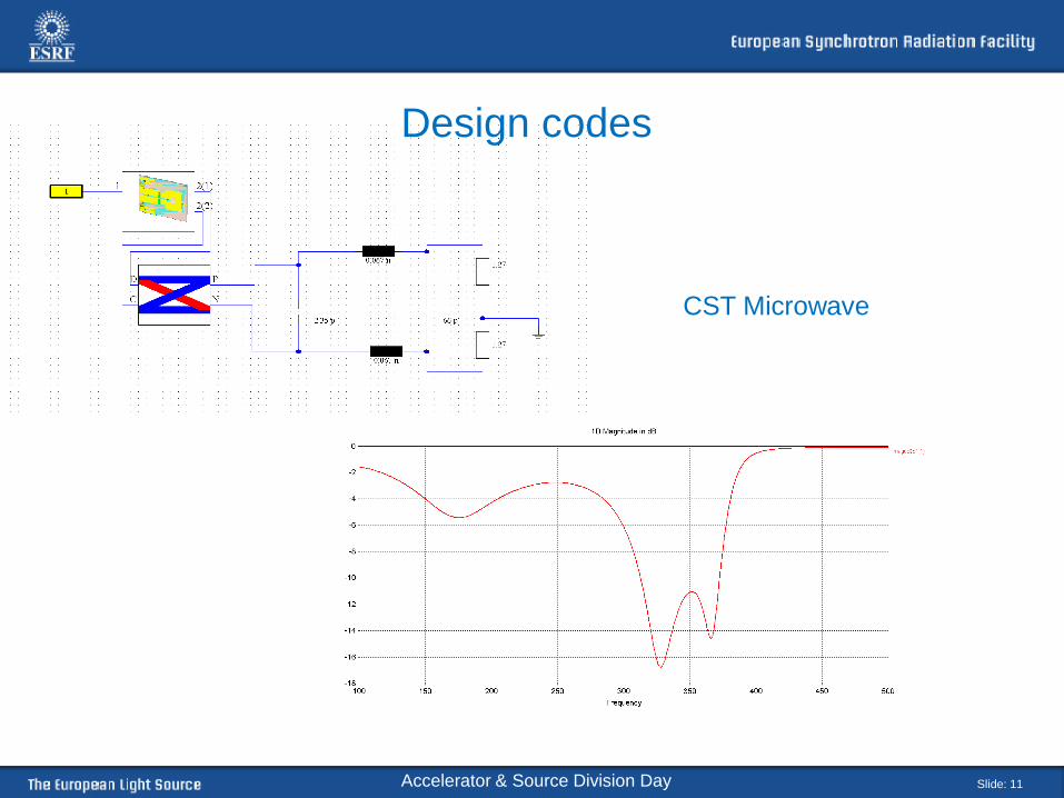
Slide: 11 Accelerator & Source Division Day
Design codes
CST Microwave

Slide: 12 Accelerator & Source Division Day
Design codes ANSOFT Designer
Port1 Cs
C46 Cp
C47
6.5e
-008
L174
6.5e
-008
L175
Cm
C178
Port1 Port2Output EqC2
Port4 Port3
Cblock1
Port4 Port3
Cblock1Port8 Port7
CapsParallel3
Port8 Port7
CapsParallel4
PortCapPrimAPortCapPrimBPortCapSecAPortCapSecB
Port1Drain1Drain2
PortCapDCA1PortCapDCA2PortCapCDB1PortCapDCB2
PortCapMAPortCapMB
BiasABiasB
BiasA2CapBiasA1CapBiasA2
BiasB2CapBiasB1CapBiasB2
Layout
0.00 100.00 200.00 300.00 400.00 500.00 600.00 700.00F [MHz]
-87.50
-75.00
-62.50
-50.00
-37.50
-25.00
-12.50
0.00
Y1
CircuitOutputScatteringXY Plot 2 ANSOFT
Curve InfodB(S(Port1,Port2))
LinearFrequencydB(S(Port1,Port3))
LinearFrequencydB(S(Port2,Port3))
LinearFrequency
Printed balun, matching circuit and bias model

Slide: 13 ESLS-RF 04/10/2011
The RF module
• A RF module has been designed at ESRF.
• It is using a printed circuit balun transformer.
• It is quite narrow (65mm)
• Very few components are necessary.

Slide: 14 ESLS-RF 04/10/2011
Experimental results
0.0
10.0
20.0
30.0
40.0
50.0
60.0
70.0
20.20
20.40
20.60
20.80
21.00
21.20
21.40
21.60
21.80
0 100 200 300 400 500
Effic
ienc
y %
Gai
n (d
B)
Output power (W)
BLF 578 V1 results
578V1 gain
578V1 eff

Slide: 15 Accelerator & Source Division Day
Experimental results
The matching capacitances are far too
hot to ensure reliable operation. The one on the
balun reached some 140°C.

Slide: 16 Accelerator & Source Division Day
Experimental results
We tried to split the capacitances in many
small ones. We air cooled it from
above.
No way, another design was needed!!!

Slide: 17 Accelerator & Source Division Day
New output circuit
The capacitance on the balun was suppressed.
The matching circuit cap has a modest value.
The price to be paid is extra length.
It is currently in low level test.

Slide: 18 Accelerator & Source Division Day
New output circuit
Above : S parameters computed with CST
microwave Below: S parameters
measured with the R&S network analyzer
Note: the matching capacitance has been
readjusted
-50.0
-40.0
-30.0
-20.0
-10.0
0.0
10.0
0.0 100.0 200.0 300.0 400.0 500.0
S (d
B)
Frequency (MHz)
Spara magnitude 578V2Out Cm=27pF at exact spot
S11 S dif-1 Scom-1

Slide: 19 ESLS-RF 04/10/2011
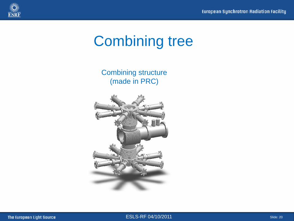
Combining tree
Implementation of solid state amplifiers at SOLEIL
Slide: 20 ESLS-RF 04/10/2011
Combining tree
Combining structure (made in PRC)

Slide: 21 ESLS-RF 04/10/2011
The cavity combiner
E010 mode
E field H field

Slide: 22 ESLS-RF 04/10/2011
The cavity combiner : advantages
1290 mm
997 mm
e.g: 6*22 modules of 650 W~ 80 kW
1. Small footprint

Slide: 23 ESLS-RF 04/10/2011
The cavity combiner : advantages
4. Efficient One stage of coupling, moreover in waveguide mode, generate less
losses than multiple stages.
2. Galvanic insulation Each pallet is connected to a loop protruding inside the cavity. Live
conductors from each pallet are thus insulated from each other. 3. Flexible
In the event of an overrating of the power, it is possible and easy to connect a fraction of the available openings, blinding the other ones with short-circuits.
Adjusting the number of modules to the power need enhances efficiency since each module is used at nominal power and not at reduced power.
5. Proven A combiner for 2 IOT’s,150 kW, 500 MHz has been designed,
manufactured and tested at THALES for ALBA.

Slide: 24 ESLS-RF 04/10/2011
The cavity combiner : status
• A full size model has been designed at ESRF.
• It is meant for 3 columns of 6 rows. • The parts were delivered in February • The variable waveguide connection
was delivered in April. • It was tested at low level.

Slide: 25 Accelerator & Source Division Day
The cavity combiner : low level results
1 is the waveguide output terminated with
a WR 2300 to N transition.
3 is one of the input ports.
The matching can be perfectly trimmed.

Slide: 26 Accelerator & Source Division Day
The cavity combiner : low level results
The theoretical value is -12.55 dB
-13.2
-13
-12.8
-12.6
-12.4
-12.2
-12 0 2 4 6 8
S1j i
n dB
Lines
S1j by columns
port2-7
port8-13
port14-19 23.1719
21, =∑
=iiS
The theoretical value would be √18 A dubious contact was seen on the
movable short circuit.

Slide: 27 Accelerator & Source Division Day
The cavity combiner : low level results
With the 2 adjustments foreseen,
the output could be matched to either 1 or
2, or 3 columns of loaded ports.
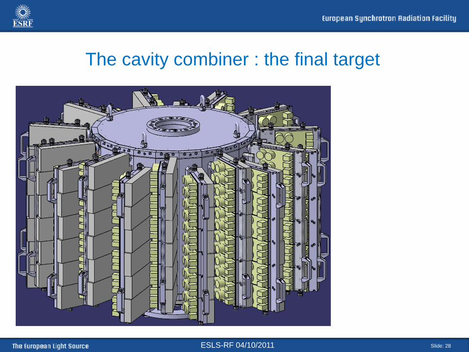
Slide: 28 ESLS-RF 04/10/2011
The cavity combiner : the final target

Slide: 29 ESLS-RF 04/10/2011
Thanks!
•To my RF colleagues, for their continuous support.
•To Nora, the lovely and efficient student we had for 5 months.
•To Francois Villar who did the mechanical design of the
combiner
•To the purchasing department.


