31
Joe O’Hare, Marketing Director Sanjeev Aggarwal, Ph.D., VP Manufacturing & Process SEMICON Taipei SOLVING MANUFACTURING CHALLENGES AND BRINGING SPIN TORQUE MRAM TO THE MAINSTREAM 9/4/2015
Joe O’Hare, Marketing Director Sanjeev Aggarwal, Ph.D., VP Manufacturing & Process
SEMICON Taipei
SOLVING MANUFACTURING CHALLENGES AND BRINGING SPIN TORQUE MRAM
TO THE MAINSTREAM
9/4/2015

SEMICON Taipei
Everspin Company Highlights
2 9/4/2015

SEMICON Taipei
The Opportunity for MRAM
Current Mainstream Memory is One-Dimensional.
RAM is fast, but is also “Volatile”.
FLASH is “Non-Volatile”, but is also slow, limited endurance, and requires high power.
A complex system is required for “Persistent RAM” or “High-Integrity NVM”.
The Market for “Persistent RAM” and “High-Integrity NVM” will be ~$5B by 2019.
We address this market with Discrete and Embedded MRAM technology.
We are optimizing the memory for Embedded Integration (>20Bu TAM by 2018).
Magnetoresistive RAM, a.k.a. “MRAM”
3 9/4/2015

Everspin Company Highlights
4
The Market Leader in Advanced MRAM Products and Solutions
Serves Large and Growing Markets ($2B+ Toggle & Spin Torque MRAM TAM in 2018)
Well-Established OEM Relationships (Dell, Avago, Siemens, Bosch, BMW, Fujitsu…)
Global, Cost Effective Operations
500+ Patents & Applications Worldwide, 350+ Patents Granted Worldwide
Strong Financial Track Record and Privately Owned by Semiconductor VCs
Proven Quality and Reliability, Qualified by Numerous Tier One (Fortune 50) Companies
Increased R&D Focus on ST-MRAM in Advanced Technology Nodes (40/28nm and beyond)
Mass-Proliferation of ST-MRAM through GLOBALFOUNDRIES Partnership
Optimizing MRAM Technology for Embedded Integration
Discrete MRAM
Systems MRAM
Embedded MRAM
SEMICON Taipei 9/4/2015

9/4/2015 SEMICON Taipei
Part One- Solving Manufacturing Challenges
ST-MRAM background 64Mb in-plane ST-MRAM in Production 64Mb with pMTJ 256Mb and 1Gb ST-MRAM on 300mm Manufacturing Summary
5

ST-MRAM Technology
SEMICON Taipei 6
Write with current passing through the MTJ
Higher memory density with shrinking MTJ bit size
Perpendicular MTJ (pMTJ) bits enable higher density compared to in- plane MTJ (iMTJ) bits
9/4/2015

In-plane vs Perpendicular ST-MRAM
Magnetic thin films want to be in-plane magnetized (de-magnetization fields)
Stable states defined bit shape: limits of shape anisotropy requires larger bits for good data retention
The reference layer is pinned and the anti-parallel configuration of the SAF is intrinsically stable
Few materials with stable magnetization direction perpendicular to the film plane
Energy barrier is determined by the material and not shape of the bits. Can achieve high Eb with small bits
Pinning is less effective and not used. It is possible to ‘break’ the SAF causing hard failure of the device
7 SEMICON Taipei
In-plane Perpendicular
9/4/2015

200mm, 90nm node Si
64Mb in-plane ST-MRAM in Production
SEMICON Taipei 9/4/2015

ST-MRAM is in Production and Proven in the Market
SEMICON Taipei 9
MTJ bit is integrated in the last 2 Cu layers
Spin Torque MTJ bit (in plane)
9/4/2015

Switching distribution plots
SEMICON Taipei 10
The programming voltage Vw of an array of bits for a given write error rate is higher than the average switching voltage Vc
9/4/2015
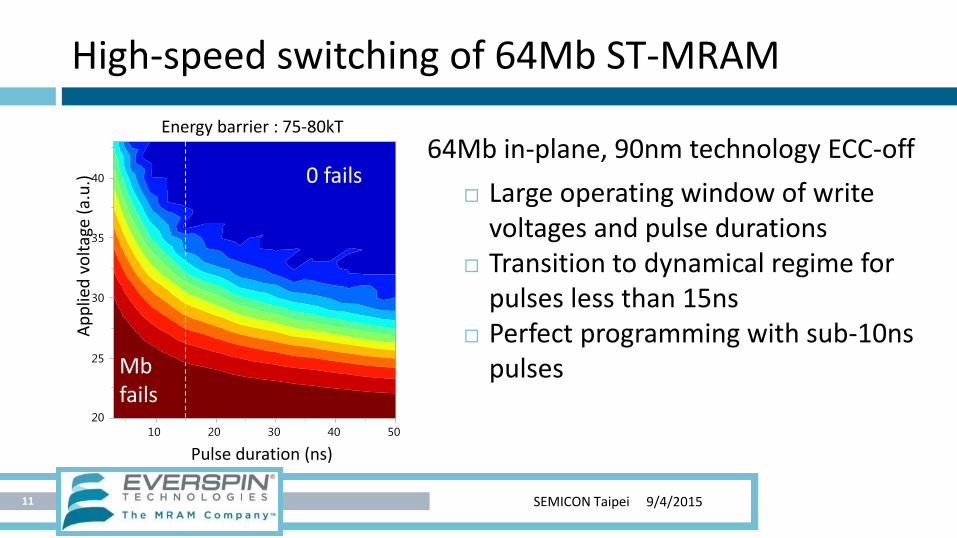
High-speed switching of 64Mb ST-MRAM
Large operating window of write voltages and pulse durations
Transition to dynamical regime for pulses less than 15ns
Perfect programming with sub-10ns pulses
11 SEMICON Taipei
Ap
plie
d v
olt
age
(a.u
.)
Pulse duration (ns)
0 fails
Mb fails
Energy barrier : 75-80kT
64Mb in-plane, 90nm technology ECC-off
9/4/2015
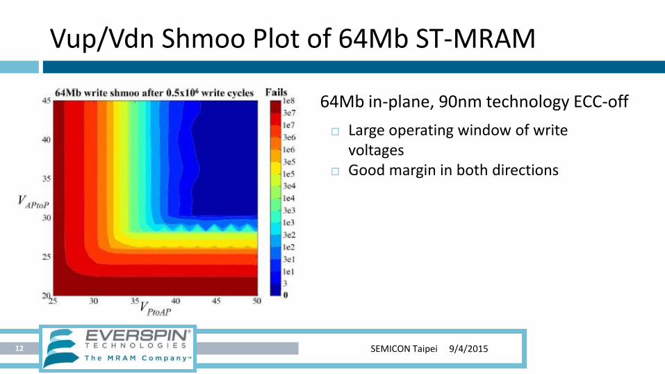
Vup/Vdn Shmoo Plot of 64Mb ST-MRAM
Large operating window of write voltages
Good margin in both directions
12 SEMICON Taipei
64Mb in-plane, 90nm technology ECC-off
9/4/2015

Endurance
SEMICON Taipei 13
64Mb iMTJ parts have better than 1e9 full memory cycles of endurance.
9/4/2015

200mm, 90nm node Si
64Mb Perpendicular ST-MRAM
SEMICON Taipei 9/4/2015
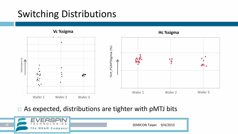
Switching Distributions
SEMICON Taipei 15
As expected, distributions are tighter with pMTJ bits
Hc %sigma Vc %sigma
Wafer 2
3 Wafer 3
Wafer 1 Wafer 2 Wafer 3
Wafer 1
9/4/2015

Switching Reliability of Large Arrays
SEMICON Taipei 16
CFB based free layers with increasing PMA
Excessive PMA causes unreliable switching for in-plane free layer
Switching reliability of fully perpendicular free layers exceeds that of in-plane free layers
Applied voltage (a.u.)
In-plane free layer with excessive PMA
In-plane free layer Perpendicular free layer
Applied voltage (a.u.) Applied voltage (a.u.)
Wri
te e
rro
r ra
te (
sigm
a)
9/4/2015
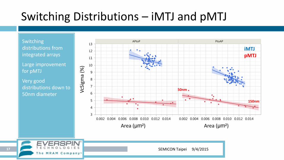
Switching Distributions – iMTJ and pMTJ
SEMICON Taipei 17
Switching distributions from integrated arrays
Large improvement for pMTJ
Very good distributions down to 50nm diameter
VcS
igm
a (%
)
Area (μm²) Area (μm²)
50nm
150nm
iMTJ pMTJ
9/4/2015
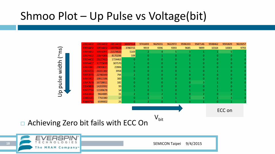
Shmoo Plot – Up Pulse vs Voltage(bit)
SEMICON Taipei 18
Achieving Zero bit fails with ECC On
16 20 24 28 32 36 40 44 48 52 56 60
0 33554432 33554432 33554432 30097314 9741693 9629231 9622972 9596333 9587146 9598462 9591829 9619257
4 33554432 33554432 33376029 3780715 9919 9396 9393 9685 9899 10164 10003 9793
8 33554432 33554391 21574920 5169 2 4 5 3 1 1 5 1
12 33554432 33544305 8170296 108 0 1 0 0 0 0 0 1
16 33554432 33137413 1724463 0 0 0 0 1 0 0 0 0
20 33554427 31773690 307570 1 0 0 0 1 0 0 0 0
24 33554381 29093611 22806 0 0 0 0 0 0 0 0 0
28 33554236 26331382 3958 0 0 0 0 1 0 1 0 0
32 33553573 22780349 794 2 0 0 0 0 0 0 0 0
36 33551822 19911596 300 0 0 0 0 0 0 0 0 0
40 33547678 16728811 182 0 0 0 1 0 3 1 0 0
44 33540898 14203992 99 0 1 0 0 0 0 1 0 1
48 33527714 11599678 54 1 0 1 0 1 0 1 0 0
52 33510350 9664885 31 2 0 2 0 0 2 0 2 1
56 33480185 7763380 17 0 1 3 1 1 4 1 3 0
60 33446715 6599002 25 0 2 0 1 0 1 0 1 2
Up
pu
lse
wid
th (
~ns)
Vbit
ECC on
9/4/2015

256Mb In-plane ST-MRAM, 40nm node Si 1Gb Perpendicular ST-MRAM, 28nm node Si
300mm Development
SEMICON Taipei 9/4/2015
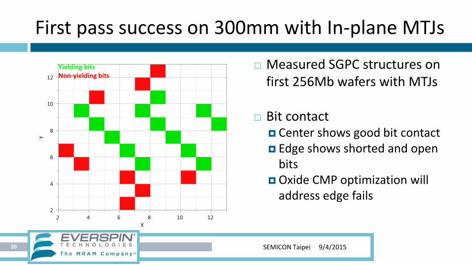
First pass success on 300mm with In-plane MTJs
20 SEMICON Taipei
Measured SGPC structures on first 256Mb wafers with MTJs
Bit contact Center shows good bit contact Edge shows shorted and open
bits Oxide CMP optimization will
address edge fails
Yielding bits Non-yielding bits
9/4/2015

Successful Demonstration of MTJ Device
21 SEMICON Taipei
Arrays on MTJs High speed switching
1
1.1
1.2
1.3
1.4
1.5
1.6
1.7
1.8
1.9
2
-6 -4 -2 0 2 4 6
Res
ista
nce
(a.
u.)
Field (a.u.)
0
0.2
0.4
0.6
0.8
1
1.2
0 0.5 1 1.5 2
Swit
chin
g p
rob
abili
ty
Voltage (a.u.)
9/4/2015
Summary
SEMICON Taipei 22
Fully-functional 64Mb DDR3 ST-MRAM 90nm node in production In-plane MTJ material optimized for low Vc and good switching
In-plane technology successfully transferred to GF 300mm for 256Mb product on 40nm node.
Perpendicular MTJ development focus on 300mm Several similarities in process and materials between iMTJ and pMTJ 35% improvement in distributions compared to in-plane Scaling to 1Gb product on 300mm, 28nm node Si
9/4/2015

SEMICON Taipei
Part Two- Bringing MRAM to the Mainstream
The MRAM Market Opportunity Everspin Takes MRAM to the Mainstream
MRAM is Proven and Shipping
Embedded MRAM Conclusion
23 9/4/2015

TAM compilation from Everspin, Semicast, Databeans, & Markets&Markets
Secure & Reliable Smart Grid
Power Fail Safety for HDD and RAID
Instantly Recoverable Transportation Systems
Fault-Recoverable Industrial Automation
16M MRAM
256K MRAM
1M MRAM
4M MRAM
256M (in test)
64M QSPI (in dev)
64M DDR3
4Gb (future)
More Reliable Storage, File, & Backup Systems
Rapid, Low Latency Enterprise Storage & Networks
1Gb (in dev)
Mainstream Persistent DRAM in Consumer Applications
24
The Market for MRAM
9/4/2015

9/4/2015 SEMICON Taipei
Expanding Market Opportunity as MRAM is Accepted and Proven
25
7 Yrs
500+ 100+ 200+
50 M
MRAM Production
Cumulative MRAM
Shipments
Customer Apps
Design Wins Per Year
Everspin Customers

MRAM is Proven and Shipping
26
Strategic Investment
DDR3 and DDR4 controller optimization NVMe and storage protocol optimization
Evaluation platforms and technology demos
Meeting the quality and supplier excellence needs of leading storage, industrial, and automotive customers
300mm Wafer Production of Everspin MRAM Products ST-MRAM process transfer successful
Initial 256Mb 40nm product is functional Acceleration of pMTJ based products in 28nm and smaller
Versatile embedded memory with eMRAM
9/4/2015
9/4/2015 SEMICON Taipei
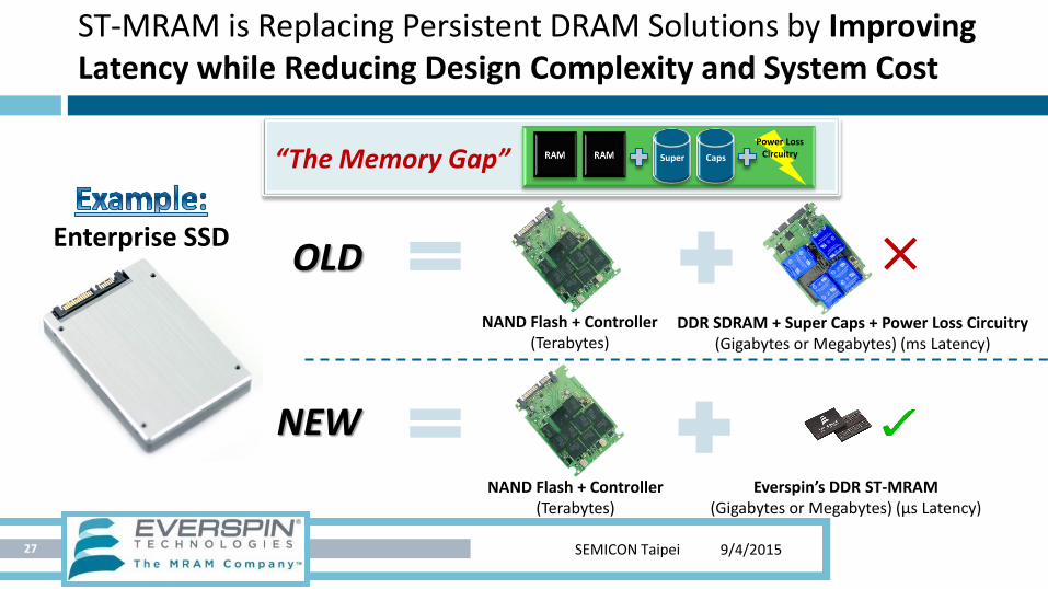
ST-MRAM is Replacing Persistent DRAM Solutions by Improving Latency while Reducing Design Complexity and System Cost
27
NAND Flash + Controller (Terabytes)
DDR SDRAM + Super Caps + Power Loss Circuitry (Gigabytes or Megabytes) (ms Latency)
OLD
NAND Flash + Controller (Terabytes)
Everspin’s DDR ST-MRAM (Gigabytes or Megabytes) (µs Latency)
NEW
Enterprise SSD
Super Caps
Power Loss Circuitry “The Memory Gap”

Scalability & Versatility: eMRAM can Replace Multiple Embedded Memory Types through Bit Cell Design Optimization
SEMICON Taipei 28
Versatility by Design:
eMRAM is unique in that the bit cell design can be modified for optimization as a replacement for Embedded FLASH, DRAM, SRAM or a combination up to all three.
As Embedded FLASH: eMRAM offers Better Endurance, Bandwidth, and Energy
As Embedded SRAM, DRAM: eMRAM offers Smaller and with Non-Volatility
As Embedded Flash + SRAM: eMRAM replaces program code + execute code + storage space with one memory
9/4/2015

9/4/2015 SEMICON Taipei
Where We’re Heading
29
300mm Capacity, Gigabit+ Densities
Data Integrity and Security in Cloud
Compute, Storage, and Server
$100M ST-MRAM Revenue by 2018
125ºC AEC-Q100 Grade 1, Cost-Down, QSPI
Reliability for Harsh Environments such
as Auto, Aerospace, Transportation
2X Toggle
MRAM Revenue by 2017
Major Foundry, Turn-Key Macro, Beyond 40nm
MCU, GPU, ARM serving IoT, Mobile,
Networking, Auto, Industrial
21Bu eMRAM
TAM by 2018
Source: IC Insights

Bringing MRAM to the Mainstream: Discrete and Embedded
SEMICON Taipei 30
MRAM is penetrating the discrete mainstream memory market.
The Market for “Persistent RAM” will be >$2B by 2018.
MRAM is the ideal next-generation mainstream embedded memory.
Market potential for Embedded MRAM is greater than 20 Billion units worldwide by 2018.
MRAM is scalable and versatile, beyond existing eFLASH (40nm) and eSRAM (20nm) solutions.
Everspin is the MRAM Company and the only company:
To bring MRAM to the market, both discrete and embedded (7 years, 50Mu+)
With 200mm and 300mm (GLOBALFOUNDRIES) MRAM production lines
With a commercialized Spin Torque MRAM solution (64Mb) & roadmap to Gigabit density
Enabling embedded ST-MRAM (300mm, advanced technology nodes)
9/4/2015
THANK YOU
SEMICON Taipei 31 9/4/2015


