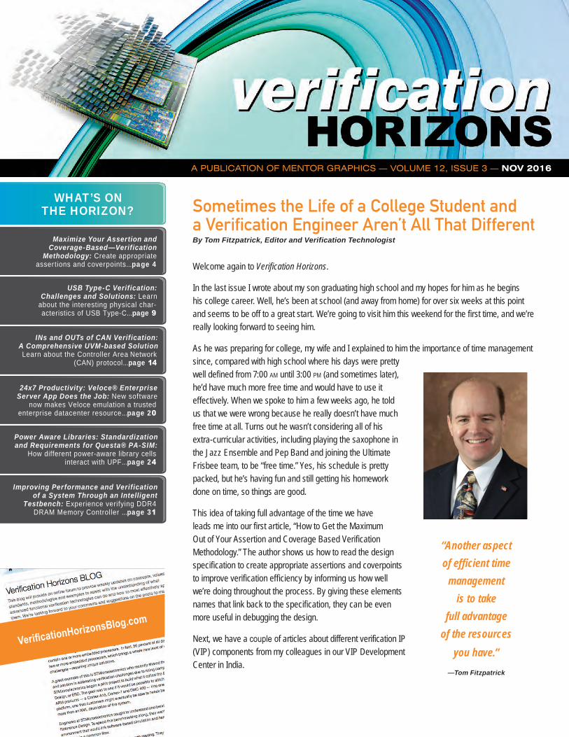
Sometimes the Life of a College Student and a Verification Engineer Aren’t All That Different By Tom Fitzpatrick, Editor and Verification Technologist Welcome again to Verification Horizons. In the last issue I wrote about my son graduating high school and my hopes for him as he begins his college career. Well, he’s been at school (and away from home) for over six weeks at this point and seems to be off to a great start. We’re going to visit him this weekend for the first time, and we’re really looking forward to seeing him. As he was preparing for college, my wife and I explained to him the importance of time management since, compared with high school where his days were pretty well defined from 7:00 AM until 3:00 PM (and sometimes later), he’d have much more free time and would have to use it effectively. When we spoke to him a few weeks ago, he told us that we were wrong because he really doesn’t have much free time at all. Turns out he wasn’t considering all of his extra-curricular activities, including playing the saxophone in the Jazz Ensemble and Pep Band and joining the Ultimate Frisbee team, to be “free time.” Yes, his schedule is pretty packed, but he’s having fun and still getting his homework done on time, so things are good. This idea of taking full advantage of the time we have leads me into our first article, “How to Get the Maximum Out of Your Assertion and Coverage Based Verification Methodology.” The author shows us how to read the design specification to create appropriate assertions and coverpoints to improve verification efficiency by informing us how well we’re doing throughout the process. By giving these elements names that link back to the specification, they can be even more useful in debugging the design. Next, we have a couple of articles about different verification IP (VIP) components from my colleagues in our VIP Development Center in India. A PUBLICATION OF MENTOR GRAPHICS — VOLUME 12, ISSUE 3 — NOV 2016 Maximize Your Assertion and Coverage-Based—Verification Methodology: Create appropriate assertions and coverpoints...page 4 WHAT’S ON THE HORIZON? USB Type-C Verification: Challenges and Solutions: Learn about the interesting physical char- acteristics of USB Type-C...page 9 Improving Performance and Verification of a System Through an Intelligent Testbench: Experience verifying DDR4 DRAM Memory Controller ...page 31 INs and OUTs of CAN Verification: A Comprehensive UVM-based Solution Learn about the Controller Area Network (CAN) protocol...page 14 24x7 Productivity: Veloce® Enterprise Server App Does the Job: New software now makes Veloce emulation a trusted enterprise datacenter resource...page 20 Power Aware Libraries: Standardization and Requirements for Questa® PA-SIM: How different power-aware library cells interact with UPF...page 24 “Another aspect of efficient time management is to take full advantage of the resources you have.” —Tom Fitzpatrick
Transcript
Sometimes the Life of a College Student and a Verification Engineer Aren’t All That Different By Tom Fitzpatrick, Editor and Verification Technologist
Welcome again to Verification Horizons.
In the last issue I wrote about my son graduating high school and my hopes for him as he begins his college career. Well, he’s been at school (and away from home) for over six weeks at this point and seems to be off to a great start. We’re going to visit him this weekend for the first time, and we’re really looking forward to seeing him.
As he was preparing for college, my wife and I explained to him the importance of time management since, compared with high school where his days were pretty well defined from 7:00 am until 3:00 pm (and sometimes later), he’d have much more free time and would have to use it effectively. When we spoke to him a few weeks ago, he told us that we were wrong because he really doesn’t have much free time at all. Turns out he wasn’t considering all of his extra-curricular activities, including playing the saxophone in the Jazz Ensemble and Pep Band and joining the Ultimate Frisbee team, to be “free time.” Yes, his schedule is pretty packed, but he’s having fun and still getting his homework done on time, so things are good.
This idea of taking full advantage of the time we have leads me into our first article, “How to Get the Maximum Out of Your Assertion and Coverage Based Verification Methodology.” The author shows us how to read the design specification to create appropriate assertions and coverpoints to improve verification efficiency by informing us how well we’re doing throughout the process. By giving these elements names that link back to the specification, they can be even more useful in debugging the design.
Next, we have a couple of articles about different verification IP (VIP) components from my colleagues in our VIP Development Center in India.
A PUBLICATION OF MENTOR GRAPHICS — VOLUME 12, ISSUE 3 — NOV 2016
Maximize Your Assertion and Coverage-Based—Verification
Methodology: Create appropriate assertions and coverpoints...page 4
WHAT’S ON THE HORIZON?
USB Type-C Verification: Challenges and Solutions: Learn
about the interesting physical char-acteristics of USB Type-C...page 9
Improving Performance and Verification of a System Through an Intelligent
Testbench: Experience verifying DDR4 DRAM Memory Controller ...page 31
INs and OUTs of CAN Verification: A Comprehensive UVM-based Solution Learn about the Controller Area Network
(CAN) protocol...page 14
24x7 Productivity: Veloce® Enterprise Server App Does the Job: New software
now makes Veloce emulation a trusted enterprise datacenter resource...page 20
Power Aware Libraries: Standardization and Requirements for Questa® PA-SIM:
How different power-aware library cells interact with UPF...page 24
“Another aspect of efficient time
management is to take
full advantage of the resources
you have.”—Tom Fitzpatrick
2
The first article, is a relatively new protocol in “USB Type-C Verification: Challenges and Solutions” where we learn about the interesting physical character-istics of USB Type-C. Because the USB Type-C connector is reversible and can connect to either hosts or devices, there are a number of new factors that must be verified, including mixed-signal issues. Our QVIP wraps all of these verification features in a convenient easy-to-use component that lets you verify and debug designs for this next-generation of the USB standard.
We round out our QVIP session with “INs and OUTs of CAN Verification: A Comprehensive UVM-based Solution” in which we learn about the Controller Area Network (CAN) protocol, popular in automotive applications. As you’ll see, there are a number of verification challenges inherent in the protocol that are handled easily by the QVIP component. I think you’ll find interesting the discussion of our QVIP Configurator tool, a GUI-based tool that lets you generate an instance of the QVIP to fit in your specific UVM testbench environment.
Another aspect of efficient time management is to take full advantage of the resources you have. In “24x7 Productivity: Veloce® Enterprise Server App Does the Job,” my colleague Vijay Chobisa, from Mentor’s Emulation Division, shows us how this new software app makes Veloce emulation a trusted enterprise datacenter resource. In this article you’ll learn about the powerful new features available for concurrent projects worldwide to enhance emulator usage and maximize not only your time, but your investment as well.
For those of you doing low-power design and verification, you’ll find “Power Aware Libraries: Standardization and Requirements for Questa PA-SIM” to be particularly interesting. This article examines several different types of power-aware library cells and how they interact with the Unified Power Format (UPF) standard. You’ll see how Questa PA-Sim can take advantage of some new power-aware libraries to seamlessly augment your power-aware verification.
We wrap up this issue with our Partners’ Corner, from our friends at Arastu Systems, who share their thoughts on “Improving Performance and Verification of a System Through an Intelligent Testbench.” The article shares their experience of verifying their DDR4 DRAM Memory Controller and how they created two new verification components to handle critical aspects of the verification. It’s a slightly different interpretation of “Intelligent Testbench,” but I think you’ll find it valuable.
Now it’s time for me to pack for my weekend trip to see David. I’ve been given some constraints and assertions by my wife, and I’m about to run to the store to fill some “coverage holes” for my travel kit. By the time you read this, I’ll be home from my visit and looking forward to seeing him when he comes home for Thanksgiving. We’re going to pack as much as we can into our time together this weekend. I hope you take some time to be with your family too.
Respectfully submitted, Tom Fitzpatrick Editor, Verification Horizons
3
Verification Horizons is a publication of Mentor Graphics Corporation, all rights reserved.
Editor: Tom FitzpatrickProgram Manager: Rebecca GranquistWilsonville Worldwide Headquarters8005 SW Boeckman Rd.Wilsonville, OR 97070-7777Phone: 503-685-7000
To subscribe visit: www.mentor.com/horizonsTo view our blog visit:VERIFICATIONHORIZONSBLOG.COM
USB Type-C Verification: Challenges and Solution by Suraj Parkash Gupta and Zeeshan Yousuf, Mentor Graphics
Page 14INs and OUTs of CAN Verification—A Comprehensive UVM-based Solution by Saumya Agrawal, Mentor Graphics
Page 2024 x 7 Productivity: Veloce Enterprise Server App Does the Job by Vijay Chobisa, Mentor Graphics
Page 24Power Aware Libraries: Standardization and Requirements for Questa® Power Aware by Progyna Khondkar, Mentor Graphics
Partners’ Corner Page 31Improving Performance and Verification of a System Through an Intelligent Testbench by Umesh Patel and Dhaval Shah, Arastu Systems Pvt. Ltd.
Table of Contents November 2016 Issue
Page 4How to Get the Maximum Out of Your Assertion and Coverage Based Verification Methodology by Nitish Goel, Mentor Graphics
Page 9
4
With ever increasing design complexities, ASIC and SoC (system on chip) design verification has become the biggest challenge for design and verification engineers. Various Hardware Description Languages (HDLs), like Verilog, VHDL, and SystemVerilog, and verification methodologies, like UVM and OVM, have facilitated the task of verifying designs. Despite this, bugs are still missed in the verification/validation phases, which eventually leads to a re-spin of the entire chip. Verification environments that assist with the right set of assertions and coverpoints not only increase the verification efficiency, but also aids the verification engineer to ensure that the functionality of the IP has been met according to design specifications. This article gives insight into how to capture assertions and coverpoints and how they should be written in order to achieve maximum design verification robustness.
INTRODUCTION Assertions are a set of expressions which indicate an error if some set of conditions are violated. They are used to catch those errors which must not happen. They check a specific behavior and display a message if an error occurs. They monitor for bad behavior in the design under test (DUT), and can be used to generate a warning or an error message. Assertion-based verification (ABV) has been used in past decades. Finding the right set of assertions is critical to avoid any bug escapes in the final SoC and ASIC development chips. Cover points, on the other hand, give a measure of the completeness of the design verification and its progress. Coverage metrics tell us what portion of the design has been activated during simulation. They identify portions of the design that were never activated during the process of simulation, which allows us to adjust and control our input stimulus. Hence, in this article, we cover how to find appropriate assertions and coverpoints by reading the design specification. We have used the Serial ATA (SATA) storage protocol design specification as the reference.
ASSERTION-BASED VERIFICATION ABV has been successfully applied at multiple levels of design and verification abstraction, ranging from high-level assertions within transaction-level test benches down to implementation-level assertions synthesized into emulation and hardware. They can be grouped into three categories.
Simple assertions: These capture precise lines from the specification. This set signifies those design functionalities that should not be infringed and should be fired immediately in case of any violation. The rules that are stated as “shall be/must be” in the specification should be captured as part of simple assertions.
Advanced assertions: These are interpreted from the reading of the specification. They capture the higher abstraction level of the design that is to be verified. These can also be interpreted as logical assertions.
Harmless assertions: These result in a warning rather than an error. The specification states that the design functionality is not affected even if some of the conditions are violated. Hence, these violations are given as a warning to the user. The rules that are stated as “can be/may be” in the specification should be captured as part of this set.
It is imperative that the verification engineer who is designing and configuring the verification architecture captures all three types of assertions. These sets are required to target different domains. It is in the control of the user which set should be enabled while running the simulation. Users verifying the core IP design can enable all three sets. Users with IP designs of a higher abstraction level can enable only simple and advanced sets; whereas FPGA customers enable only the simple set targeting an exact property. Care should be taken that every design specification is captured, as most of the debugging of a design can be done by capturing the right set of assertions.
Some assertions are not captured while reading the specification. These assertions are then added and planned in the next phase when specification maturity gets developed; for example, after completing the first phase of verification.
ASSERTIONS NAMING AND DESCRIPTION Writing assertions involves a name along with the description and the section of the specification from where it has been written. The right naming and description is important since it aids in debugging the design efficiently. The name should be as precise as possible and should also convey the design functionality that has been violated. It is advised to use appropriate abbreviations while naming.
How to Get the Maximum Out of Your Assertion and Coverage Based Verification Methodology by Nitish Goel, Mentor Graphics
5
This keeps the name short and at the same time coveys its meaning. The name of the assertion can start with the name of the protocol, followed by the layer name (if it is a layered protocol), then followed by the erroneous condition.
The description should match the exact line of the specification along with a brief message for the user. The message should print the actual scenario that has occurred in comparison with the benchmark scenario that is expected in the appropriate format. The section of the specification should be specified so that the user can refer directly to that part of the design specification in case of any mismatch.
The following examples show how the three sets of assertions should be captured and written.
Simple Assertions
Assertion 1
Figure 1. Serial ATA specification snippet from physical layer (PL) section 7.7.1.3
Assertion name: SATA_PL_INVLD_COMRST Assertion description: The OOB COMRESET shall consist of no less than six data bursts. X number of burst received. Assertion section: 7.7.1.3
In this assertion, the validity of the COMRESET signal is checked. It shall consist of no less than six data bursts. If the COMRESET signal with data burst less than six is received, this assertion will fire. The assertion description informs the user of the actual numbers of bursts received.
Assertion 2
Figure 2. Serial ATA specification snippet from link layer (LL) section 9.5.1
Assertion name: SATA_LL_CONT_BYT0_COM Assertion description: CONT primitive detected with byte 0 as COMMA character. ALIGN represents the only primitive that contains COMMA character. Assertion section: 9.5.1
In this assertion, it is specified that only the ALIGN primitive contains the COMMA character. If any other primitive is received with byte 0 as the COMMA character, then the assertion is fired, as this is a violation.
Advanced Assertions
Assertion 1
Figure 3. Serial ATA specification snippet from physical layer (PL) section 7.7.1.3
Assertion name: SATA_PL_ALIGN_H2D_BEF_873_US Assertion description: The host should allow for at least 873.8 µs (32 768 nominal Gen1 Dword times) after detecting the release of COMWAKE to receive the first ALIGNP from the device. Hence the host should not start transmitting ALIGNP before this interval. Assertion section: 7.7.1.3
This assertion is an advanced assertion since it is interpreted from the specification. In SATA protocol, the host cannot send the ALIGN primitive before the device sends it. The host should wait for at least 873.8 µs to receive the first ALIGN from the device. It cannot send ALIGN during that interval; hence this condition should be asserted if violated.
How to Get the Maximum Out of Your Assertionand Coverage Based Verification Methodologyby Nitish Goel, Mentor Graphics
6
Assertion 2
Figure 4. Serial ATA specification snippet from transport layer (TL) section 10.5.9.1
Assertion name: SATA_TL_DMA_STUP_FIS_D_1_WHN_A_1 Assertion description: D bit detected as 1 when A bit is set to 1 in DMA Setup FIS from device to host. D bit should be 0; i.e. data is transmitted from host to device when A is set to 1 in DMA Setup FIS. Assertion section: 10.5.9.1
This assertion checks the value of D bit in DMA Setup FIS when A bit is set to 1. If D bit is 1, then there is violation of the specification and the assertion should be fired. This is an advanced assertion since the condition is not explicitly specified. It is interpreted from the specification.
Assertion 3
Figure 5. Serial ATA specification snippet
from physical layer (PL) section 8.4.2 (Fig 258)
Assertion name: SATA_PL_DEV_CONT_DR_COMINIT Assertion description: Device is continuously sending COMINIT when host is in HR_AwaitNoCOMINIT state. Possibly it is stuck in DR_COMINIT state. Assertion section: 8.4.2
This assertion verifies a complex scenario where the device is stuck in a state and is continuously sending the COMINIT signal. It is important to have a set of assertions related to state transitions of the DUT to check whether the DUT is hung up or stuck in a particular state.
Assertion 4
Figure 6. Serial ATA specification snippet from physical layer (PL) section 8.4.3 (Fig 259)
Assertion name: SATA_PL_HOST_CONT_COMRESET Assertion description: Host is continuously sending COMRESET when device is in DR_Reset state. Possibly it is stuck in HR_Reset state. Assertion section: 8.4.3 (Fig 259)
This assertion verifies the host where the host is stuck in a reset state and is continuously sending the COMRESET signal to the device which is keeping the device in the reset state. These kinds of situations are erroneous and should be asserted.
Harmless Assertions
Assertion 1
Figure 7. Serial ATA specification snippet from application layer (AL) section 13.6.4.3.1
Assertion name: SATA_AL_RD_FPDMA_QUEUE_REG_D2H_FIS_STTS_BIT4_NT_1 Assertion description: When Host transmits READ FPDMA QUEUED command, the Register Device to Host FIS sent by the device with BSY and DRQ set to 0, and error field specifying the type of error, Status Bit 4 may be 1. Assertion section: 13.6.4.3.1
In this assertion, Bit 4 in the FIS may be set to 1. Hence this is not the condition that should be strictly met and hence its violation will not lead to an error.
7
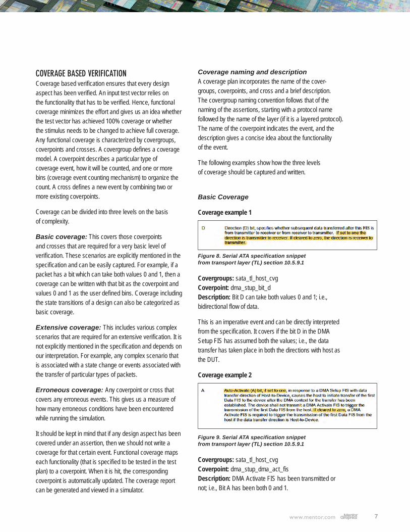
COVERAGE BASED VERIFICATION Coverage based verification ensures that every design aspect has been verified. An input test vector relies on the functionality that has to be verified. Hence, functional coverage minimizes the effort and gives us an idea whether the test vector has achieved 100% coverage or whether the stimulus needs to be changed to achieve full coverage. Any functional coverage is characterized by covergroups, coverpoints and crosses. A covergroup defines a coverage model. A coverpoint describes a particular type of coverage event, how it will be counted, and one or more bins (coverage event counting mechanism) to organize the count. A cross defines a new event by combining two or more existing coverpoints.
Coverage can be divided into three levels on the basis of complexity.
Basic coverage: This covers those coverpoints and crosses that are required for a very basic level of verification. These scenarios are explicitly mentioned in the specification and can be easily captured. For example, if a packet has a bit which can take both values 0 and 1, then a coverage can be written with that bit as the coverpoint and values 0 and 1 as the user defined bins. Coverage including the state transitions of a design can also be categorized as basic coverage.
Extensive coverage: This includes various complex scenarios that are required for an extensive verification. It is not explicitly mentioned in the specification and depends on our interpretation. For example, any complex scenario that is associated with a state change or events associated with the transfer of particular types of packets.
Erroneous coverage: Any coverpoint or cross that covers any erroneous events. This gives us a measure of how many erroneous conditions have been encountered while running the simulation.
It should be kept in mind that if any design aspect has been covered under an assertion, then we should not write a coverage for that certain event. Functional coverage maps each functionality (that is specified to be tested in the test plan) to a coverpoint. When it is hit, the corresponding coverpoint is automatically updated. The coverage report can be generated and viewed in a simulator.
Coverage naming and description A coverage plan incorporates the name of the cover- groups, coverpoints, and cross and a brief description. The covergroup naming convention follows that of the naming of the assertions, starting with a protocol name followed by the name of the layer (if it is a layered protocol). The name of the coverpoint indicates the event, and the description gives a concise idea about the functionality of the event.
The following examples show how the three levels of coverage should be captured and written.
Basic Coverage
Coverage example 1
Figure 8. Serial ATA specification snippet from transport layer (TL) section 10.5.9.1
Covergroups: sata_tl_host_cvg Coverpoint: dma_stup_bit_d Description: Bit D can take both values 0 and 1; i.e., bidirectional flow of data.
This is an imperative event and can be directly interpreted from the specification. It covers if the bit D in the DMA Setup FIS has assumed both the values; i.e., the data transfer has taken place in both the directions with host as the DUT.
Coverage example 2
Figure 9. Serial ATA specification snippet from transport layer (TL) section 10.5.9.1
Covergroups: sata_tl_host_cvg Coverpoint: dma_stup_dma_act_fis Description: DMA Activate FIS has been transmitted or not; i.e., Bit A has been both 0 and 1.
8
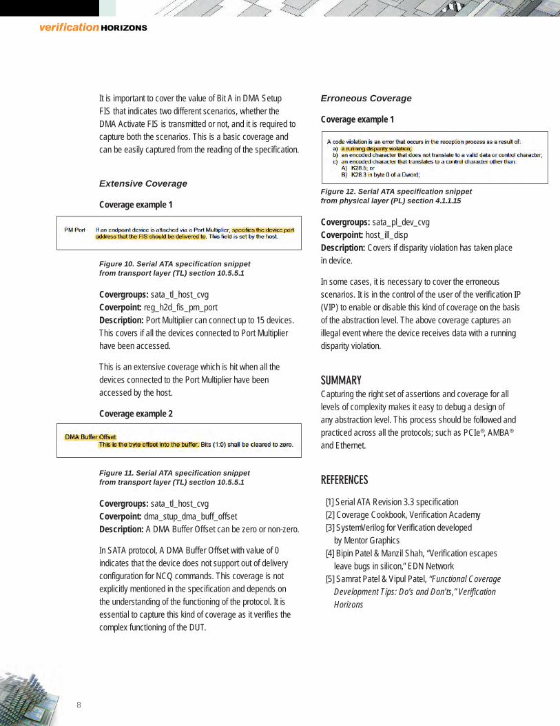
It is important to cover the value of Bit A in DMA Setup FIS that indicates two different scenarios, whether the DMA Activate FIS is transmitted or not, and it is required to capture both the scenarios. This is a basic coverage and can be easily captured from the reading of the specification.
Extensive Coverage
Coverage example 1
Figure 10. Serial ATA specification snippet from transport layer (TL) section 10.5.5.1
Covergroups: sata_tl_host_cvg Coverpoint: reg_h2d_fis_pm_port Description: Port Multiplier can connect up to 15 devices. This covers if all the devices connected to Port Multiplier have been accessed.
This is an extensive coverage which is hit when all the devices connected to the Port Multiplier have been accessed by the host.
Coverage example 2
Figure 11. Serial ATA specification snippet from transport layer (TL) section 10.5.5.1
Covergroups: sata_tl_host_cvg Coverpoint: dma_stup_dma_buff_offset Description: A DMA Buffer Offset can be zero or non-zero.
In SATA protocol, A DMA Buffer Offset with value of 0 indicates that the device does not support out of delivery configuration for NCQ commands. This coverage is not explicitly mentioned in the specification and depends on the understanding of the functioning of the protocol. It is essential to capture this kind of coverage as it verifies the complex functioning of the DUT.
Erroneous Coverage
Coverage example 1
Figure 12. Serial ATA specification snippet from physical layer (PL) section 4.1.1.15
Covergroups: sata_pl_dev_cvg Coverpoint: host_ill_disp Description: Covers if disparity violation has taken place in device.
In some cases, it is necessary to cover the erroneous scenarios. It is in the control of the user of the verification IP (VIP) to enable or disable this kind of coverage on the basis of the abstraction level. The above coverage captures an illegal event where the device receives data with a running disparity violation.
SUMMARY Capturing the right set of assertions and coverage for all levels of complexity makes it easy to debug a design of any abstraction level. This process should be followed and practiced across all the protocols; such as PCIe®, AMBA® and Ethernet.
REFERENCES
[1] Serial ATA Revision 3.3 specification[2] Coverage Cookbook, Verification Academy[3] SystemVerilog for Verification developed
by Mentor Graphics[4] Bipin Patel & Manzil Shah, “Verification escapes
Development Tips: Do’s and Don’ts,” VerificationHorizons
9
The standard USB connector that we are most familiar with is USB Type-A. Even as the USB data interface moved from USB1 to USB2 and then to USB3, the connector has remained the same. It is a massive connector and plugs in only one way.
These limitations are resolved by the USB Type-C connector. In addition to its flexibility and small size, the USB Type-C connector handles the larger power requirements of today’s USB ports. It also supports a variety of different protocols using “alternate modes,” which allows using adapters that can output HDMI, VGA, Display Port, or other types of connections from a single USB port.
The main advantages of a USB Type-C connector are:
• Transports up to 100 W of power• Removes user confusion about plug orientation• Supports legacy USB standards, such as USB2.0,
USB3.1, and USB Power Delivery (PD)• Provides alternate-mode support for standards
like HDMI, VGA, Display Port, etc.
For these reasons, the USB Type-C connector is expected to replace existing USB, power, and display related connectors on tablets, laptops, and desktops.
This article describes the challenges faced in the verification of USB Type-C connectors and of USB Type-C connectors integrated with USB PD. It also provides insights into how Questa® Verification IP (QVIP) with mixed-signal SystemVerilog constructs helps overcome these challenges.
INTRODUCING USB TYPE-C USB Type-C is a 24-pin reversible-plug connector for USB devices and USB cabling. The USB Type-C connectors connect to both hosts and devices, replacing various Type-A and Type-B connectors.
Figure 1: The USB Type-C connector
This double-sided connector provides pins for super-speed data, high-speed data, cable orientation detection, and dedicated BMC configuration data channels for USB PD communications. Connecting an older device to a host with a USB Type-C receptacle requires a cable or an adapter with a USB Type-A or Type-B plug or receptacle on one end and a USB Type-C plug on the other end.
While the USB Type-C interconnect no longer physically differentiates plugs on a cable as being either an USB A-type or B-type, the USB interface still maintains a host-to-device logical relationship.
The standard concept for setting up a valid connection between a source and sink is based on being able to detect terminations residing in the product being attached. USB Type-C involves cable orientation detection and establishment of the power roles (source-sink) and data
Figure 2: USB Type-C connector pin usage
USB Type-C Verification: Challenges and Solution by Suraj Parkash Gupta and Zeeshan Yousuf, Mentor Graphics
10
Figure 4: USB Type-C functional model
roles (host-device). Both of these require monitoring of the voltage (V), resistance (R), and current (I) values on the configuration channel (CC) pins of the connector.
With the USB Type-C connector, a source may implement higher source current to enable faster charging of mobile devices. The USB host and hubs advertise the level of current presently available via the CC pins. Three current levels are defined by the USB Type-C standard at the default VBUS:
• Default values, as defined by a USB standard(500 mA for USB2.0 ports, 900 mA for USB3.1 ports)
• 1.5 A• 3.0 A
Figure 3: USB Type-C source/sink roles are established
with pull-up (Rp) and pull-down (Rd) resistors
Initially, a source exposes independent pull-up (Rp) terminations on its CC1 and CC2 pins, and a sink exposes independent pull-down (Rd) terminations on its CC1 and CC2 pins. The source-to-sink combination of this circuit
configuration represents a valid connection. Once the sink is powered, the sink monitors CC1 and CC2 for a voltage greater than its local ground. The CC pin that is at a higher voltage (i.e., pulled up by Rp in the source) indicates the orientation of the plug, and a valid connection is established.
VERIFICATION CHALLENGES The key challenges faced in the verification of USB Type-C designs and their integration with USB PD have to do with these features:
• Establishment of the initial power (source-to-sink)relationship using the two (CC1 and CC2) pins on theUSB Type-C receptacle
• Establishment of the initial data (host-to-device)relationship using the two (CC1 and CC2) pins on theUSB Type-C receptacle
• Plug orientation and cable twist detection- Un-flipped straight-through connection (CC1 with CC1)- Flipped straight-though connection (CC2 with CC2)- Un-flipped twisted-through connection (CC1 with CC2)- Flipped twisted-through connection (CC2 with CC1)
• Collision resolution- This is required when both the ports try to act as
source (or sink). In this case, the collision needs tobe resolved by making sure that one of the two portsbacks out and decides to take up the other role, sothat a source-sink connection can be established.
11
• USB Type-C VBUS current range detection- Default value (500 mA for USB2 and 900mA
for USB3.1)- 1.5 A- 3.0 A
• USB PD communication- The USB PD Bi-phase Mark Coded (BMC)
communications are carried on the CC wireof the USB Type-C cable.
• Set up and manage power and accessory modes• Dynamic detach detection and re-attach
- In this scenario, the source monitors the attachedCC pin and the sink monitors the VBUS to detect detach.
• VCONN detection- Since only a single CC pin position (either CC1
or CC2) within each plug of the cable is connectedthrough the cable, the other CC pin that is notconnected through the standard cable is repurposedto the source Vconn to supply power to the localplug. Initially, the source supplies Vconn and thesource of Vconn can be swapped using USB PDVconnSwap.
All these features need to be verified thoroughly to make sure that a USB Type-C design works properly. This requires constant monitoring and resolution of the current (I), resistance (Rp, Rd, and Ra), and voltage (V) values on the CC1 and CC2 pins of the receptacle. Thus the verification IP must be capable of performing mixed-signal simulations. Since the USB PD communication also happens on the connected CC pin, the verification IP must also provide a seamless method of integrating USB Type-C interfaces with USB PD interfaces.
QUESTA VERIFICATION IP SOLUTION Using the latest constructs of SystemVerilog mixed signal modeling, QVIP provides a user-friendly solution to the USB Type-C verification challenges and the integration of USB Type-C with USB PD. QVIP also provides a ready-to-use exhaustive test suite (along with functional coverage) for both USB Type-C and USB PD, enabling complete verification of USB Type-C and USB PD features.
Figure 5: USB Type-C and PD QVIP integration with DUT
Following are the main features provided by QVIP.
• Source-sink detection and dynamic power roleswitching- QVIP provides flexibility to configure the initial
power role of the QVIP and starts advertising/monitoring current and voltage accordingly.Once the roles are decided based on the resultantvoltage on the CC pins, QVIP also provides flexibilityto switch the power roles (source-to-sink and vice-versa) dynamically.
• Host-device detection and dynamic data role switching- QVIP provides flexibility to configure the initial data
role of the QVIP, and once the power connectionis established, the QVIP starts operating in theconfigured role. QVIP also provides flexibility toswitch the data roles (host-to-device and vice- versa) dynamically.
• Plug orientation and twisted cable detection- Using mixed signaling constructs of SystemVerilog,
the QVIP is able to detect the USB Type-C plugorientation and establish the connection accordingly.QVIP also provides flexibility of straight and twistedcable connections.
• Collision resolution- Based on the current and resistance values
advertised by the two ports on the CC1 andCC2 pins, it is possible that the resolution mightnot happen if both ports want to operate as source(and similarly if both ports want to operate as sink).In this case, QVIP provides collision resolutionby switching its role and drives the CC1/CC2 pinsaccording to the switched role.
12
• USB PD communication- QVIP provides a seamless integration of USB
Type-C with USB PD. Once the USB Type-Cconnection has been established, the USB PDcommunications are enabled.
• Accessory modes support- QVIP supports all types of accessories (audio,
debug, and powered). QVIP can also be configuredto operate as one of the accessories.
• Dynamic detach- While the USB PD communications are in progress,
it is possible that the USB Type-C connection mightget lost, due to the absence of VBUS or a changein current. QVIP is able to handle these situations,and it also provides flexibility to switch roles duringre-attach.
• Error injection- QVIP provides support for different types
of error injection in the USB Type-C signalingand USB PD communications.
• Data recovery- The USB PD standard defines the unit interval
in the range of 3.03 µs to 3.70 µs, which meansthat the bit width of the data transmittedcan lie in this range. QVIP is capableof receiving the data sent at anyfrequency within this range. QVIPalso provides configuration to gen- erate the data at varying frequencies.
• QVIP as policy engine- QVIP can be configured to operate
as the policy engine where the CC linewill not be driven by QVIP. Instead theQVIP will provide instructions to thePHY DUT about the packets to betransmitted and will take appropriateactions after receiving any packet.
• Sequence library- QVIP provides an exhaustive test plan to verify
the DUT. More than 150 sequences are providedin the test plan. Each sequence provides the optionfor randomization of various fields and an errorinjection capability.
• Functional coverage- QVIP provides functional coverage for both USB
PD and USB Type-C to ensure that all cornercases get covered. Certain modes of USB Type-Ccoverage can also be switched-off basedon the DUT supported configuration.
Figure 6: USB PD functional coverage
Figure 7: USB Type-C functional coverage
• Scoreboarding- Data integrity checks are performed
on the USB PD data transfers.• Ease of debugging
- QVIP provides various debug options to makethe debugging easier, which includes a transactionlogger, USB Type-C signals in waveform,and protocol assertions.
13
Figure 8: Transaction logger
Figure 9: USB Type-C signaling
CONCLUSION “The Type-C plug is a big step forward,” says Jeff Ravencraft, chairman of the USB Implementers Forum (USB-IF), the organization that oversees the USB standard. “It might be confusing at first during the transition, but the Type-C plug could greatly simplify things over time by consolidating and replacing the larger USB connectors.” This clearly shows that USB Type-C is the way forward. Questa Verification IP provides an easy and user friendly solution for the verification of USB Type-C and USB PD features.
QVIP provides a solution to the mixed signal verification challenges involved with USB Type-C signaling. The comprehensive sequence library reduces the stimulus generation time, and easy debug components reduce debugging and verification time.
To learn more about QVIP, you can visit several whitepapers on mentor.com, including Verifying Display Standards – A comprehensive UVM based Verification IP Solution and Verification IP Stimulus APIs – Are They Really Easy to Use?
REFERENCES
[1] USB Type-C Specification Release 1.2,March 25, 2016
[2] USB Power Delivery Specification Revision 2.0,V1.2, August 2, 2016
[3] USB Type-C Port Controller InterfaceSpecification, Revision 1.0, V1.1, July 2016
14
Automotive vehicles are not only fast moving, but also have various systems comprising a variety of advanced technologies. Increasing complexities of these systems need much more sophisticated components and interactions.
Amongst the various standards that target the automotive IP section, CAN holds a unique place. CAN (controller area network) is a communication protocol which uses a single, shared serial bus and supports distributed real time multiplexing for use within a variety of road/space applications.
Various nodes that connect on the bus can have different oscillator frequencies but all coordinate in a manner such that a network-wide time quantum and, eventually, bit time is achieved.
Designing of such a system is sophisticated, but the verification of a CAN node or CAN system brings many more challenges and complications.
This article explains the challenges in the verification of a CAN node and how CAN Questa® Verification IP combats those.
INTRODUCTION Fast moving vehicles have even faster moving technology and complex systems. Increased complexity of the system is due to sophisticated components and complicated interactions between them. In an automotive environment, where the IP is supposed to be fast as well as very precise, the need for perfect verification increases.
The more advanced version of automotive protocols is found in space and aeronautic applications where the precision needed increases by many folds.
The automotive industry protocols include Controller Area Network (CAN), Local Interconnect Network (LIN), Flexray, and others. All these have an in-built similarity in their architectures.
All have a serial bus, which is shared between various nodes, master/slaves, and, for the case of multiple transmitters at a particular time, arbitration mechanisms are defined.
We will keep the description and details limited to Controller Area Network (CAN) in this article.
HISTORY Controller area network is a serial communication protocol which supports distributed real-time control and multiplexing for use within road vehicles and other control applications.
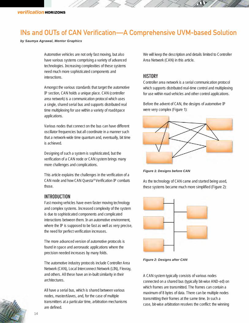
Before the advent of CAN, the designs of automotive IP were very complex (Figure 1):
Figure 1: Designs before CAN
As the technology of CAN came and started being used, these systems became much more simplified (Figure 2):
Figure 2: Designs after CAN
A CAN system typically consists of various nodes connected on a shared bus (typically bit-wise AND-ed) on which frames are transmitted. The frames can contain a maximum of 8 bytes of data. There can be multiple nodes transmitting their frames at the same time. In such a case, bit-wise arbitration resolves the conflict: the winning
INs and OUTs of CAN Verification—A Comprehensive UVM-based Solutionby Saumya Agrawal, Mentor Graphics
15
node continues transmission and the losing node stops transmitting and becomes a receiver of that message. The node that lost arbitration can retry the message at a later point.
The widespread usage of CAN resulted in a demand for more bandwidth at greater speed. In order to realize this, a new protocol, CAN-FD, was introduced which could carry a data payload of up to 64 bytes and support an option to carry the data at a higher speed.
Another important characteristic of a CAN system is the timing and re-synchronizations that enable a number of nodes with different oscillator frequencies to work together in a system with a shared bus.
The next section describes in detail the challenges associated with CAN system verification.
VERIFICATION CHALLENGES From the previous section, we saw that a CAN system simplifies the connections, design, and organization of the system manifolds, but the verification of CAN nodes still remains a challenging task.
There are multiple challenges involved in the verification of the CAN bus.
1) The first basic requirement is to correctly follow thesynchronizations and re-synchronizations happeningon the bus so that the data sampled by a verificationcomponent is the actual value of data rather than beinga false sample due to incorrect sampling. It is a majorrequirement to correctly achieve this synchronizationas there may be multiple nodes with different oscillatorfrequencies.
2) The correct verification of a CAN interface requirescovering all interesting scenarios so as to check thefunctionality of the bus in each and every corner case.Missing any of these may leave a possible bug in theIP. The possibility of a potential failure presents a verybig risk due to the presence of the IP in componentsthat carry human lives (CAN is used in automotivespace or military/aeronautics) or cost intensive projects(space requirements) where it is extensively used.
3) A node may be error active or error passive. A node’sbehavior on the bus is dependent on this. Hence, it isvery important to verify that the node works fine in allthe corner cases for both scenarios.
4) Even if a particular node of a system is a passiveerror node, the other nodes of the system could stillbe in active mode. In such a case, the amalgam of theactivity on the interface gives rise to an even greaternumber of interesting scenarios which are necessaryto verify.
5) Error handling, which is a very big factor in theverification of any IP, holds an even greater importancein CAN. There are various error conditions supportedin CAN. A verification component must subject theCAN IP under verification with all such possiblestimulus and at the same time create combinations ofthese erroneous situations with various bit fields and/ornode situations.
6) Because a node losing arbitration will become areceiver of the frame, it needs to be thoroughly verifiedfor the continuous correct flow of information.
7) The CAN specification allows different behaviors forthe transmitter and receiver of a frame. This differencecan be seen in valid bit values, inter frame gaps, errorhandling, and so on.
8) When CAN-FD enabled nodes are verified, itscombination with classical and CAN-FD tolerant nodesneeds to be checked. A CAN-FD node must be ableto correctly decode as well as generate both classicaland FD frames.
Apart from the above major challenges, the other general challenges of set up of a re-usable verification environment, quick turn-around times, efficient utilization of the bus, and others still hold true.
Considering these and other challenges confronting the fast growing automotive industry, it is inevitable that a comprehensive and precise verification solution is needed.
This article goes through a solution provided by Questa® Verification IP (QVIP) that targets all the issues specified above so that a verification engineer is able to verify their design effectively.
INs and OUTs of CAN Verification—A Comprehensive UVM-based Solutionby Saumya Agrawal, Mentor Graphics
16
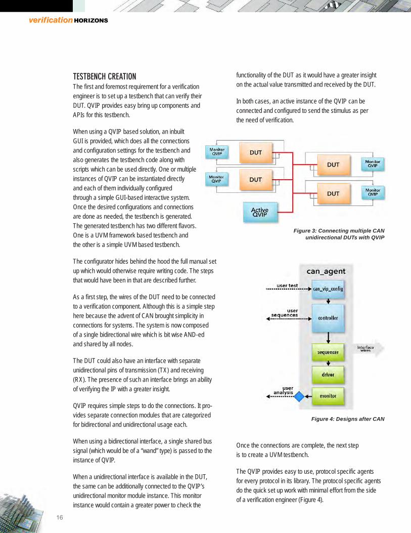
TESTBENCH CREATION The first and foremost requirement for a verification engineer is to set up a testbench that can verify their DUT. QVIP provides easy bring up components and APIs for this testbench.
When using a QVIP based solution, an inbuilt GUI is provided, which does all the connections and configuration settings for the testbench and also generates the testbench code along with scripts which can be used directly. One or multiple instances of QVIP can be instantiated directly and each of them individually configured through a simple GUI-based interactive system. Once the desired configurations and connections are done as needed, the testbench is generated. The generated testbench has two different flavors. One is a UVM framework based testbench and the other is a simple UVM based testbench.
The configurator hides behind the hood the full manual set up which would otherwise require writing code. The steps that would have been in that are described further.
As a first step, the wires of the DUT need to be connected to a verification component. Although this is a simple step here because the advent of CAN brought simplicity in connections for systems. The system is now composed of a single bidirectional wire which is bit wise AND-ed and shared by all nodes.
The DUT could also have an interface with separate unidirectional pins of transmission (TX) and receiving (RX). The presence of such an interface brings an ability of verifying the IP with a greater insight.
QVIP requires simple steps to do the connections. It pro- vides separate connection modules that are categorized for bidirectional and unidirectional usage each.
When using a bidirectional interface, a single shared bus signal (which would be of a “wand” type) is passed to the instance of QVIP.
When a unidirectional interface is available in the DUT, the same can be additionally connected to the QVIP’s unidirectional monitor module instance. This monitor instance would contain a greater power to check the
functionality of the DUT as it would have a greater insight on the actual value transmitted and received by the DUT.
In both cases, an active instance of the QVIP can be connected and configured to send the stimulus as per the need of verification.
Figure 3: Connecting multiple CAN unidirectional DUTs with QVIP
Figure 4: Designs after CAN
Once the connections are complete, the next step is to create a UVM testbench.
The QVIP provides easy to use, protocol specific agents for every protocol in its library. The protocol specific agents do the quick set up work with minimal effort from the side of a verification engineer (Figure 4).
17
Various static time functionalities are easily controlled via the agent itself. For example, in order to configure the QVIP to behave as an active agent, the setting of a simple switch is required. Here, a node can be configured as a CAN classical/CAN-FD/CAN-FD tolerant node.
Further examples are present in the QVIP library that explain all the use cases.
In addition to the above connection and configuration, which is elemental for all verification components alike, CAN verification needs some important information about the bit timings of the system. This is needed as it is elemental to the correct sampling of bits and, hence, eventually the functionality of the system. By providing these values, the user does not need to take care about the bit timing synchronizations any further. The biggest challenge in the verification of a CAN DUT is simply taken care by the QVIP automatically.
These are made as configurations in the CAN QVIP BFM, which can be easily specified as per the desired value and the set up of the testbench is now complete.
This three step process for the verification set up is made in a way that the simple parts of verification set up are quickly done.
STIMULUS GENERATION Stimulus generation is the critical part of CAN DUT verification. QVIP takes a lead here by providing an extensive sequence library with a list of sequences that traverse the specification with even the minutest of details.
With this easily usable set of sequences in the sequence library, one of the most difficult parts of CAN node verification is now a cake-walk. A verification engineer simply picks the desired sequence, or runs all of them together. In this way, they achieve various scenarios and test the receiver side of their DUT.
The next level of interesting scenarios involves the verification of correct functionality of the DUT reacting to scenarios in which multiple nodes (even the DUT) are transmitting at the same time. Here again, QVIP does its part very cleanly. The generation of frames by QVIP can be precisely controlled as per the need of a user. Again the
sequences provided in the sequence library can be utilized here.
For systems that are CAN–FD enabled, there is a separate set of sequences provided that exercise all flavors of the CAN-FD specification. The CAN classical sequences are also needed as a part of the complete verification of a CAN-FD node.
As repeatedly asserted before, error handling is a very critical part in the verification of a CAN node. The CAN QVIP comes with a list of sequences which generate all kinds of error scenarios that can easily subject the DUT to a variety of erroneous scenarios.
Verification engineers just need to pick the ones that they want and the error scenario gets generated.
This ready-made sequence library takes away the headache of writing the sequences for the verification engineer. The verification cycles can rather be spent in thinking of more and more ways of stress-testing the DUT and thinking of more complicated and interesting scenarios.
COVERAGE COLLECTOR Once a user starts writing the test cases, the question arises: “When is it time to say that the verification is complete?” The coverage collector plays a critical role here. The QVIP coverage collector extensively targets all the features of the specifications. All kinds of frames, frame attributes, the control variety, interesting data values, and various other flexibilities shall be verified for correct functionality as per the protocol.
The coverpoints and crosses target the specification extensively and make sure that the design can be called completely verified if it achieves 100% coverage.
In order to perform the verification in a systematic manner, the QVIP also provides a verification plan in the form of an XML file along with the coverage example. This clearly maps individual sections of the respective protocol specifications.
Typically, when debugging some issues, an engineer may not want to keep coverage enabled. QVIP provides an
18
opportunity to enable/disable coverage collection as required, using a simple switch.
PROTOCOL CHECKERS The CAN specification describes a whole set of erroneous scenarios as well as the mechanisms to recover from them.
The first requirement of a verification component is that the interface activity is checked for protocol compliance and error messages are given in case of protocol violation.
CAN QVIP provides an elaborate list of protocol checking assertions with the following features:
1) Error messages given alongside the assertion firingcontain a detailed description about what part of theinterface activity violated the specification. The errormessages are tagged with proper references givenfor the specification section that defines the correctbehavior.
2) Ability to enable/disable individual/all assertions.Ideally speaking, none of the assertions should bedisabled, but when specific negative scenarios arebeing targeted, it comes useful to disable the specificerror checks.
3) SystemVerilog Assertion (SVA) capabilitiessuch as wave-level debug and assertion coverage.
4) Transaction-level items which contain the erroneouspart of the violation get highlighted when seen in theGUI. This makes the debug and analysis of assertionseasier by many folds.
The checkers are a typical feature of all verification IP. What demarks the QVIP from others is the amount of debug options that come with the QVIP which makes the identification as well as the resolution of issues easier.
Checkers and their additional flexibilities given by the QVIP come really handy in CAN where this can be used
to see that all type of erroneous scenarios get exercised and perform various kinds of detailed analysis of the failing cases.
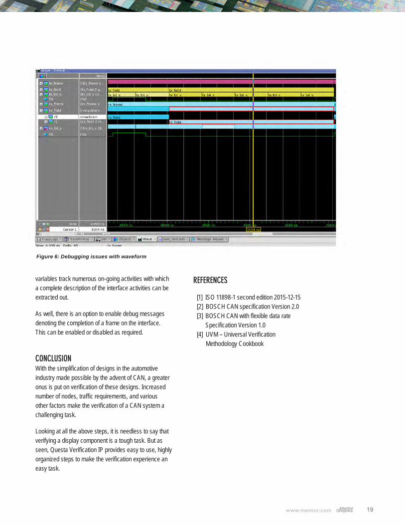
DEBUGGING ISSUES There are multiple issues/challenges faced in the debugging of CAN interface issues:
1) A single bit does not traverse the interface in oneclock unit (time quantum). It takes multiple time quanta(TQ) to send one bit across the interface. The numberof TQs increase/decrease slightly on the account ofsynchronizations/resynchronizations. Hence it becomeshard to keep track of the number of actual bits traversedif a verification engineer tries to debug just with thesignals.
2) With the large number of frames involved in asimulation, the frame boundaries need to be correctlyidentified, and this adds to the debug difficulty.
3) An added flavor of complexity comes from the factthat a node may be transmitting but loses arbitrationfrom some other currently running node. This needs tobe correctly tracked as the behavior of many featureschange if a node was the transmitter of the previousframe.
The CAN QVIP deals with all these issues very gracefully. While debugging a CAN simulation, transaction-level items can be seen in the GUI that traverse one complete nominal or data bit (as the case may be). Also, the frame sequence items show complete boundaries of their time of existence on the interface. Another useful feature is a parent-child relationship between the frame items and the fields and thereafter the individual bits that constitute the frame.
QVIP maintains a complete track of the arbitration wins/losses (when a unidirectional interface is available), so that a verification engineer gets a deeper insight into the current happenings on the bus. This and various other status
# ** Error: (vsim-60007) MVC @ 3202 ns: /top/node1/can_if rx_field: CAN_STUFF_ERR_DETECTED:21 - CAN node detected a stuff error. Refer ISO 11898-1 CAN specification, section 10.11# ** Error: (vsim-60007) MVC @ 3202 ns: /top/node2/can_if rx_field: CAN_STUFF_ERR_DETECTED:21 - CAN node detected a stuff error. Refer ISO 11898-1 CAN specification, section 10.11
Figure 5: shows a sample error message from the QVIP
19
variables track numerous on-going activities with which a complete description of the interface activities can be extracted out.
As well, there is an option to enable debug messages denoting the completion of a frame on the interface. This can be enabled or disabled as required.
CONCLUSION With the simplification of designs in the automotive industry made possible by the advent of CAN, a greater onus is put on verification of these designs. Increased number of nodes, traffic requirements, and various other factors make the verification of a CAN system a challenging task.
Looking at all the above steps, it is needless to say that verifying a display component is a tough task. But as seen, Questa Verification IP provides easy to use, highly organized steps to make the verification experience an easy task.
REFERENCES
[1] ISO 11898-1 second edition 2015-12-15[2] BOSCH CAN specification Version 2.0[3] BOSCH CAN with flexible data rate
Specification Version 1.0[4] UVM – Universal Verification
Methodology Cookbook
Figure 6: Debugging issues with waveform
20
INTRODUCTION The way companies use hardware emulation has changed. Historically, emulators were used in a lab, at one location, executing one job at a time. Because of this, an emulator often sat idle. In this scenario, project scheduling for the emulator was done manually by allocating fixed time slots to project teams. An inherently inflexible and inefficient way to manage a valuable resource, especially for global teams.
Emulators are not confined to this arrangement anymore. They are now managed as a corporate-wide shared resource in a datacenter. Initially, the efforts to meet the requirements for a shared resource depended on standard job management software, such as LSF and Sun Grid. But these approaches treated emulators like any other hardware in a datacenter. The truth is that emulators are far more complex and specialized than general purpose systems. Every emulation job is different in terms of size, duration, verification requirements and priority.
To satisfy these requirements, Mentor developed the Veloce® Enterprise Server App, aka the Veloce ES App. The Veloce ES App delivers a fully-integrated solution for complete, transparent access to emulation resources worldwide for concurrent projects. It significantly enhances emulator use by delivering advanced features like suspend, resume, relocate, high priority, and large job scheduling as well as access to utilization statistics over a period of time. These unique features make Veloce emulation a trusted enterprise datacenter resource.
EMULATION WITH ENTERPRISE SERVER APP SW Understanding how a datacenter-based emulator works starts by looking at how an emulator is built. An emulator begins with a chassis. The chassis is equipped with a number of slots to support a number of boards — aka AVBs. The more boards, the more capacity and the more users running emulation concurrently. Designs are mapped to the Veloce emulator in a way that makes the most of the boards in the system.
When an emulator is used as a datacenter resource the capacity (number of boards) in the emulator becomes a shared resource, and effective job scheduling software is needed to “share” the emulation resource. In a datacenter environment, job scheduling software is just as important as the capacity of the emulator.
What is the boundary to capacity? In the context of this article, it is sufficient to know that a single Veloce chassis can support up to 2 billion gate designs and 128 simultaneous users. How can all of these users be accommodated while maximizing the productivity and quality of verification?
The answer is relatively simple, the Veloce ES App allows job management software to understand how to manage an
24 x 7 Productivity: Veloce® Enterprise Server App Does the Jobby Vijay Chobisa, Mentor Graphics
Figure 1: System flexibility minimizes idle hardware by allowing individual designs to be distributed
across emulation boards in several ways.
21
influx of emulation jobs. It serves as an interface between job management software and the Veloce hardware platform.
The Veloce ES App recognizes the configuration of the emulator and the requirements of the emulation job in the queue at any given time. It also knows what a piece of hardware can do, and where there is flexibility in the system. For example, it knows how many emulation boards are available, where they are, and what can be done with them. It also knows which users have priority, and it can suspend lower priority jobs to get more important ones done. Also it can suspend several small jobs to accommodate a bigger job — i.e., one that requires more emulation resources.
A TRANSPARENT, FLEXIBLE USE MODEL In an emulation datacenter model, it is critical that all of the job allocation activity is transparent to the verification engineer. They do not need to know, and should not be bothered with where the emulator is, how to access it, or how the various jobs in the queue are distributed and managed.
With the Veloce ES App, verification engineers simply upload their emulation jobs using normal job submission commands. Once a job is in the queue, the Veloce ES App identifies the best possible resource to run the job. Once resources become available, the job is dispatched and the resource is marked as busy. The job runs and the verification engineer gets the results. When a job is completed, the next job in the queue is started. Bottom line: No emulator downtime and no human interaction or communication is needed.
The Veloce ES App eliminates the need for managers and administrators to manually assign emulation resources, and future enhancements to the Veloce ES App are implemented such that users do not need to worry about making changes to the script or test environment.
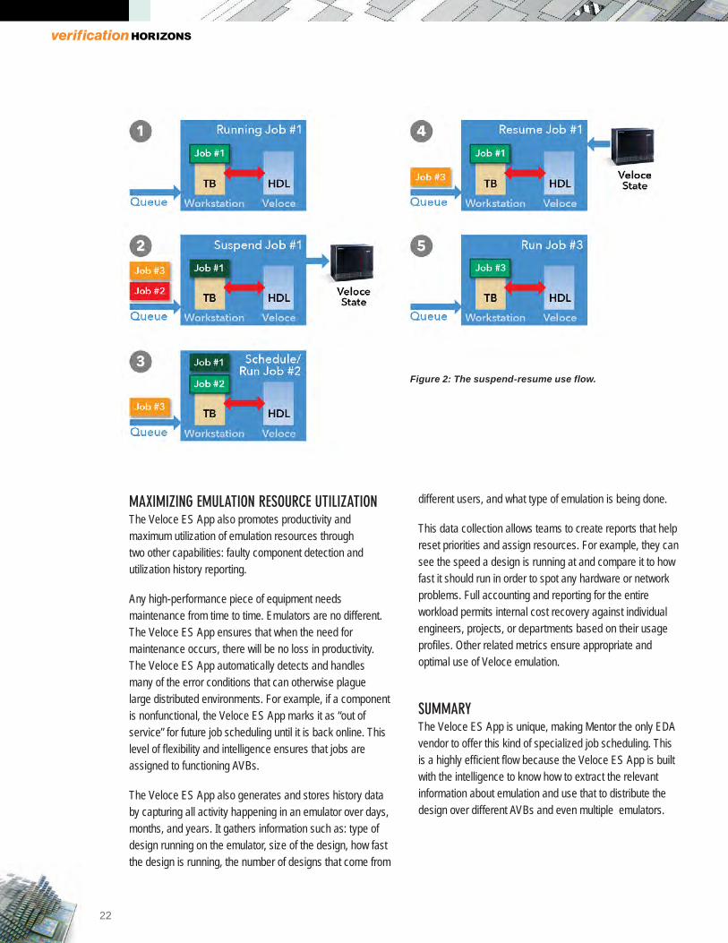
THE SUSPEND-RESUME-RELOCATE FLOW The notion of “no downtime” is reinforced by a capability unique to the Veloce emulation platform called “suspend-resume-relocate.” Suspend and resume substantially increases emulator utilization as advanced blocking of resources is not needed. In other words, the Veloce ES App enables the scheduling of low priority jobs without sacrificing performance or capacity for higher priority jobs (see Figure 2, next page).
Typically, jobs immediately go on the emulator if resources are available to run them. When a high priority job needs to run immediately, the Veloce ES App saves the entire state space of the job currently running on the emulator and suspends it in order to run the higher priority job. When the high-priority job is completed, Veloce resumes the suspended job from the exact timeframe where it was suspended.
A third capability, relocate, complements suspend and resume by transparently reassigning a suspended job to different AVBs or emulators. This gives users the flexibility to either resume a suspended job on the same emulation hardware or relocate the verification run to similar hardware that is immediately available. The capability to redistribute jobs provides optimum scheduling flexibility and maximum system availability. Suspend-resume-relocate is a testbench-agnostic capability, fully handled by the Veloce ES App, so no additional work is needed on the user’s part.
Suspend-resume-relocate allows the emulator to be used to the fullest possible extent. High priority jobs get serviced immediately, and managers do not have to worry about reserving emulator resources for high priority and time critical jobs. This feature is critical for running a scheduled big job by temporarily suspending several smaller jobs after the bigger job has waited in the queue for a specified amount of time. Ultimately, there is no loss of emulation time.
24 x 7 Productivity: Veloce® Enterprise Server App Does the Jobby Vijay Chobisa, Mentor Graphics
22
MAXIMIZING EMULATION RESOURCE UTILIZATION The Veloce ES App also promotes productivity and maximum utilization of emulation resources through two other capabilities: faulty component detection and utilization history reporting.
Any high-performance piece of equipment needs maintenance from time to time. Emulators are no different. The Veloce ES App ensures that when the need for maintenance occurs, there will be no loss in productivity. The Veloce ES App automatically detects and handles many of the error conditions that can otherwise plague large distributed environments. For example, if a component is nonfunctional, the Veloce ES App marks it as “out of service” for future job scheduling until it is back online. This level of flexibility and intelligence ensures that jobs are assigned to functioning AVBs.
The Veloce ES App also generates and stores history data by capturing all activity happening in an emulator over days, months, and years. It gathers information such as: type of design running on the emulator, size of the design, how fast the design is running, the number of designs that come from
different users, and what type of emulation is being done.
This data collection allows teams to create reports that help reset priorities and assign resources. For example, they can see the speed a design is running at and compare it to how fast it should run in order to spot any hardware or network problems. Full accounting and reporting for the entire workload permits internal cost recovery against individual engineers, projects, or departments based on their usage profiles. Other related metrics ensure appropriate and optimal use of Veloce emulation.
SUMMARY The Veloce ES App is unique, making Mentor the only EDA vendor to offer this kind of specialized job scheduling. This is a highly efficient flow because the Veloce ES App is built with the intelligence to know how to extract the relevant information about emulation and use that to distribute the design over different AVBs and even multiple emulators.
Figure 2: The suspend-resume use flow.
23
The Veloce ES App enables 24x7 utilization of emulation resources by verification teams worldwide, allowing companies to greatly reduce the total cost of ownership. It also ensures maximum use of the entire infrastructure by providing a robust, efficient, and scalable job scheduling solution that matches the most appropriate resources with the needs of the workload.
The Veloce ES App supports efficient management of the emulator resources and minimizes added cycles. A fully integrated solution, it significantly enhances administrator and engineer productivity through highly efficient, transparent job scheduling for the Veloce emulation platform. Thus, extremely valuable Veloce emulation resources are allocated to jobs according to the objectives and goals of the business, via operational policies configured by verification managers using standard job management tools like LSF, Univa, and NC.
Consequently, users typically see a 20% increase in emulation capacity with the Veloce ES App — now that’s real money.
24
INTRODUCTION Multivoltage (MV) based power-ware (PA) design verification and implementation methodologies require special power management attributes in libraries for standard, MV and Macro cells for two distinctive reasons. The first aspect is to provide power and ground (also bias) supply or PG-pin information, which is mandatory for PA verification. The second reason is to provide a distinctive attribute between a special MV cell and a regular standard cell. The special MV cells include isolation (ISO), level-shifters (LS), enable level-shifter (ELS), always-on buffers (AOB), feed through buffers or repeaters (RPT), diode clamps, retention flops (RFF), power switches (PSW), multi- and single-rail macros. This article describes the standard requirements for libraries and processing mechanism in Questa® PA-SIM from UPF-based PA verification perspective.
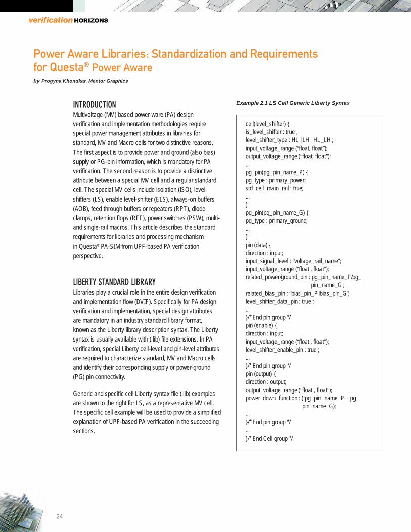
LIBERTY STANDARD LIBRARY Libraries play a crucial role in the entire design verification and implementation flow (DVIF). Specifically for PA design verification and implementation, special design attributes are mandatory in an industry standard library format, known as the Liberty library description syntax. The Liberty syntax is usually available with (.lib) file extensions. In PA verification, special Liberty cell-level and pin-level attributes are required to characterize standard, MV and Macro cells and identify their corresponding supply or power-ground (PG) pin connectivity.
Generic and specific cell Liberty syntax file (.lib) examples are shown to the right for LS, as a representative MV cell. The specific cell example will be used to provide a simplified explanation of UPF-based PA verification in the succeeding sections.
Example 2.1 LS Cell Generic Liberty Syntax
Power Aware Libraries: Standardization and Requirements for Questa® Power Awareby Progyna Khondkar, Mentor Graphics
pin_name_G);...}/* End pin group */...}/* End Cell group */
25
Example 2.2 LS Cell Specific Liberty Sample
LIBERTY POWER MANAGEMENT ATTRIBUTES The generic and specific examples given in the previous section prevails several attributes, for instance, the ‘is_level_shifter:true, level_shifter_type:HL_LH’, ‘input_voltage_range’, and ‘output_voltage_range’ are known as special cell-level attributes that categorize this particular cell as an LS. Hence when these attributes are missing, the LS will be treated as just a regular standard cell. All the remaining attributes in these examples (such as ‘pg_pin, pg_type, related_power, ground, bias_pin, std_cell_main_rail, and power_down_function’) are termed as pin-level attributes.
It is worth mentioning that some of these Liberty attributes are also implied in UPF as predefined attribute names. UPF supports the specification of attributes of objects in a design. Hence UPF allows such attributes to be used with HDL specifications in design code or with Liberty attribute specifications in a Liberty library. Table 3.1 shows a few of the Liberty attributes that are relevant to the UPF predefined attribute names.
Table 3.1 Liberty and Relevant UPF Attributes
Note: there are other such UPF attributes implied with the Liberty syntax that are not relevant to the context discussed here.
Continuing with the LS examples, the ‘pg_pin’ and ‘pg_type‘ attribute together facilitate specification of power, ground, and bias pin connectivity of the cell, which in general will correspond to the primary power (VDD, VDDO), ground (VSS), and bias (VNW, VPW) supply of the power domain where this cell actually belongs, as specified in UPF. The ‘input_voltage_range’ and ‘output_voltage_range’ are the voltage ranges (from 0.8 to 1.2 volt) for all the input or output pins of the cell under all possible operating conditions. The ‘related_power/ground_pin’ and ‘related_bias_pin’ provide the related power, ground, and bias supply connectivity information for each input or output logical port or pin of the cell.
Power Aware Libraries: Standardization and Requirementsfor Questa® Power Awareby Progyna Khondkar, Mentor Graphics
Related supply is augmented with ‘pg_pin’ attributes that indicate the functionality of the supply, whether it is primary power or primary ground. For single rail cells, when there is only a single set of power and ground supplies, all the inputs or outputs have only one set of related supplies. However for multi-rail cells, especially the MV and Macro cells, like the LS in this example (which is a MV cell), usually possesses different related supplies for the input and output. Figure 3.1 shows the diagram of LS cell explained above with related PG-pin information for all input and output pin. Here the related supplies for input pin (A) is (VDD/VSS) and for output pin (Y) is (VDDO/VSS).
Figure 3.1 Level-shifter with related PG-pin information
The ‘std_cell_main_rail’ attribute defines the primary power pin (VDD) that will be considered as the main rail. This is a power supply connectivity parameter that is required when the cell is placed and routed at the post P&R level. The ‘power_down_function’ expression identifies the Boolean condition that consists of the combination of the different statuses of the power, ground, and bias pins, which signifies when the output pin of the cell will be turned off by these power, ground, and bias pins. The ‘power_down_function’ is defined in the library exclusively for verification purposes only. More precisely, the function is entirely for UPF-based dynamic simulation, where it facilitates the verification tool to comprehend the corruption behavior for the cell when the power domain (where the cell resides) is powered-off or switched to a shutoff condition.
The corruption semantics are imposed by the PA simulator imply on internal sequential elements, input and output signals, ports, and pins of the cell to change their regular known values to unknown values, in the event of power down or inadequate power supply to drive those logics correctly. So it actually defines a rule set that decides, how
logic elements essentially behave in response to reduction and disconnection of power. Corruption typically refers to the situation where the value of logic elements or signals becomes unpredictable. Hence, corrupted logic is usually assigned to 1’bx or 1’b0 or hiz depending on logic types or user preferences.
The detail on power down functions are further discussed in succeeding sections for other library formats. Liberty libraries are mandatory for post-synthesis, gate-level PA static verification and in certain circumstances they are also required for PA dynamic simulation. From the examples and discussion above it is evident that both the cell-level and pin-level attributes are mandatory for any MV or Macro cell Liberty syntax. However, only pin-level attributes are applicable for standard cells used in PA verification, since no special attribute is required to distinguish a standard cell. UPF 2.1 and 3.0 LRM mention supporting the Liberty 2009.06 release syntax; however the latest release by the open Liberty organization is 2015.12.
POWER AWARE VERIFICATION MODEL LIBRARIES Apart from the Liberty standard library syntax, there are other formats of non-standard behavioral model libraries, mostly modeled in HDL with (.v or .vhd) file extensions. The (.v or .vhd) models are specifically required for dynamic simulation-based verification and obviously available in two different formats, PA and non-PA simulation (.v or .vhd) model libraries. Hence these libraries may or may not include the supply power and ground pin information. Standard and MV cell models are usually written as Verilog HDL modules and use constructs such as Verilog built-in primitives or user-defined primitives (UDPs) to express the relatively simple behavior of a standard cell. They may also be written as VHDL design entities (entity and architecture pairs) using VITAL package, which provides Verilog-like primitive modeling capabilities.
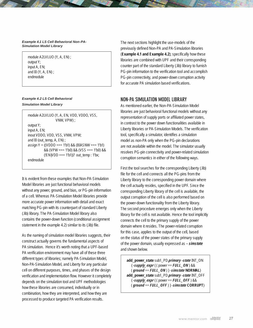
Similarly, hard macro simulation model libraries can be written in either language, using more complex behavioral constructs such as Verilog initial blocks and always blocks, or VHDL processes and concurrent statements. However, PA-Simulation Model and Non-PA-Simulation Model libraries are not standardized like the Liberty standards. The following are the examples of LS cell behavioral simulation libraries, modeled in Verilog HDL.
27
Example 4.1 LS Cell Behavioral Non-PA- Simulation Model Library
Example 4.2 LS Cell Behavioral
Simulation Model Library
It is evident from these examples that Non-PA-Simulation Model libraries are just functional behavioral models without any power, ground, and bias, or PG-pin information of a cell. Whereas PA-Simulation Model libraries provide more accurate power information with detail and exact matching PG-pin with its counterpart of standard Liberty (.lib) library. The PA-Simulation Model library also contains the power-down function (conditional assignment statement in the example 4.2) similar to its (.lib) file.
As the naming of simulation model libraries suggests, their construct actually governs the fundamental aspects of PA simulation. Hence it’s worth noting that a UPF-based PA verification environment may have all of these three different types of libraries; namely PA-Simulation Model, Non-PA-Simulation Model, and Liberty for any particular cell on different purposes, times, and phases of the design verification and implementation flow. However it completely depends on the simulation tool and UPF methodologies how these libraries are consumed, individually or in combination, how they are interpreted, and how they are processed to produce targeted PA verification results.
The next sections highlight the use-models of the previously defined Non-PA and PA-Simulation libraries (Example 4.1 and Example 4.2); specifically how these libraries are combined with UPF and their corresponding counter part of the standard Liberty (.lib) library to furnish PG-pin information to the verification tool and accomplish PG-pin connectivity, and power-down corruption activity for accurate PA simulation based verifications.
NON-PA SIMULATION MODEL LIBRARY As mentioned earlier, the Non-PA-Simulation Model libraries are just behavioral functional models without any representation of supply ports or affiliated power states, in contrast to the power down functionalities available in Liberty libraries or PA-Simulation Models. The verification tool, specifically a simulator, identifies a simulation model as non-PA only when the PG-pin declarations are not available within the model. The simulator usually resolves PG-pin connectivity and power-related simulation corruption semantics in either of the following ways.
First the tool searches for the corresponding Liberty (.lib) file for the cell and connects all the PG-pins from the Liberty library to the corresponding power domain where the cell actually resides, specified in the UPF. Since the corresponding Liberty library of the cell is available, the output corruption of the cell is also performed based on the power-down functionality from the Liberty library. The second procedure emerges only when the Liberty library for the cell is not available. Hence the tool implicitly connects the cell to the primary supply of the power domain where it resides. The power-related corruption for this case, applies to the output of the cell, based on the status of the power states of the primary supply of the power domain, usually expressed as – simstate and shown below.
module A2LVLUO (Y, A, EN) ; output Y; input A, EN; and I0 (Y, A, EN) ; endmodule
Here, it is assumed that the Non-PA-Simulation Model is instantiated with the hierarchical elements that belong to the sub1_PD power domain. There are two power states INT_ON with -simstate NORMAL when the output of the cell will remain unaffected; however, during INT_OFF with -simstate CORRUPT, the output will be corrupted. TheNon-PA-Simulation Models are well suited for modelingstandard cells with a single rail and are traditionally usedfor post-synthesis, gate-level functional verification or logicsimulation in a purely non-PA verification environment.However, they can be straightaway accommodated to thePA simulation verification environment at the post-synthesisgate-level by combining with UPF and the correspondingLiberty standard library.
PA-SIMULATION MODEL LIBRARY On the contrary, a PA-Simulation Model library completely represents all the power, ground, bias, and related supply ports or PG-pins of a cell. As well it defines the power down functionalities. The PG-pins in PA-Simulation Models are primarily defined as input and output ports; however they may also be defined as internal registers, wires, or as supply_net_type, supply0 and supply1 type, etc. Although the internal types of PG-pins are more common in an extended PA-Simulation Model library explained in the next section.
The PA-Simulation Model also includes the behavioral code that monitors the supply ports and appropriately corrupts its internal states and outputs, in response to events or values on the power supply and logic ports. However, explicit connection of an external testbench and UPF power supply to these PA model’s supply ports is mandatory through UPF connect_supply_net or connect_supply_set explicit commands. The explicit UPF connections disable the simstate-based corruption semantics, unlike non-PA models explained in the previous section. Hence Questa PA-SIM allows the PA-Simulation model library (.v) to take precedence and apply corruption semantics by itself. The simulator drives only the appropriate supply values to the PG-pin of the cell — when VDD is turned off (Example 4.2), the output Y will become 1’bx. Obviously a corresponding Liberty (.lib) library is unnecessary for PA verification with PA-Simulation model library. The PA-Simulation models are more suitable for modeling multi-rail macros and specifically they are created for PA simulation-based verification at the
post place-and-route PG-netlist level, since PG-netlists contain PG-pin connectivity as well as logical functionality of a cell.
Questa PA-SIM also supports UPF predefined attribute-based automatic connections, if a supply port has the UPF_pg_type attribute associated with it — either by an HDL attribute specification or a UPF set_port_attributes command, based upon its pg_type. In this case, the appropriate value conversion table (VCT) will also be inserted based on the pg_type of the port.
Example 4.2.1 UPF Predefined Attributes Usage in HDL
EXTENDED-PA-SIMULATION MODEL LIBRARY In addition to Non-PA-Simulation Model and PA-Simulation Model libraries, there is a combined form of functional and power aware simulation model libraries, often termed as Integrated or Extended-PA-Simulation model library. The requirements of such extended libraries comes from the distinctive verification artifacts that makes them usable for both the non-PA regular functional (logic) verification and PA verification environment, while keeping both the functional and power features active internally in both environments. This is desirable because it is sometimes convenient to have simulation models specifically for hard Macros that can be used in both of these verification environments, without adding extra levels of hierarchy and without leaving power ports unconnected. Only extended power aware simulation models makes this possible.
The fundamental power-related construction of Extended-PA models differs from PA-Simulation models in power port declaration semantics. While PA-Simulation models declare ports on the interface of the model as input or output types, Extended-PA supply ports are defined as internal wires or
For VHDL:
attribute UPF_pg_type of vdd_backup: signal is “backup_power”
registers as well as supply_net_type, supply0, and supply1 types within the HDL simulation models. The following example explains the construct of Extended-PA-Simulation model.
Example 4.3.1 A Macro Cell Behavioral Integrated or Extended-PA-Simulation Model Library
The integrated model defines only the power supplies (DVDD, VDD, DVSS, and VSS) despite of other PG-pins, including bias and related power and ground pins usually available in its counterpart in the Liberty (.lib) format. However, the supplies are defined as internal objects representing assigned default constant values that enable normal operational mode for non-PA-Simulation. During PA-Simulation with Questa PA-SIM, when UPF supply nets are connected to those internal objects through explicit connections via connect_supply_net or connect_supply_set commands or through automatic connections based on the UPF_pg_type attribute (similar
to PA-Simulation models), the UPF supply net overrides the default constant values of the model, and the model then behaves as a PA-Simulation model.
More specifically from Example 4.3.1, the power (VDD) and ground (VSS) are defined as supply1 and supply0, which complies with the UPF LRM specification for designating power as 1’b1 and ground as 1’b0 logic resolution, when both are in the On state. During PA- Simulation, Questa PA-SIM provides the connectivity to the VDD and VSS of the model with the corresponding power domain primary and ground specified in the UPF. Hence such models are readily usable in RTL (considering power as 1’b1 and ground as 1’b0 as constant values) as well as in post-synthesis gate-level PA-Simulation with UPF, where the actual physical Macro cells are already inserted (considering VDD and VSS are connecting through the UPF supply net and then they can be driven from testbench).
Even the Extended-PA-Simulation models are also usable for post-layout PG-netlist level PA-Simulation with UPF. This is because the physical connections of power and ground of the Macro cell are already available in the netlist, and UPF provides the hooks to the internally defined power (VDD) and ground (VSS) through supply net connections similar to post-synthesis gate-level PA-Simulation. It is worth mentioning here that the PG-netlist PA dynamic simulation based verification does not require UPF, when a regular PA-Simulation model is available. Table 4.3.1 summarizes the library requirements for Questa PA-SIM.
Pure RTL (.lib) – Good to have for MV, Macro (.v) Model – No
(.lib) – No (.v) Model – Yes
MV/Macro Instantiated RTL (.lib) – Yes for MV, Macro (.v) Model – Yes for MV, Macro
(.lib) – No (.v) Model – Yes for MV, Macro
Synthesis Gate-Level (GL) (.lib) – Yes (.v) Model – Yes
(.lib) – No (.v) Model – Yes
P&R/Layout PG-Netlist (.lib) – Yes (.v) Model – Yes
(.lib) – No (.v) Model – Yes
Non PG-netlist (.lib) – Yes (.v) Model – Yes
(.lib) – No (.v) Model – Yes
(.lib) – PG-pin Liberty library(.v) – PA-Simulation Model Library (fully matching PG-pin with its counterpart of Liberty library).
Table 4.3.1 PA Verification Library Requirements for Questa PA Sim
30
It is distinctive at this point that Extended-PA-Simulation models have greater adaptability in different simulation environments and in different levels of design abstraction — from RTL to PG-netlist. However, depending on the verification targets and objectives, particularly for PA verification, all four types of libraries may become relevant and useful. Although the requirements of these libraries differ, depending on design abstraction levels, both the Liberty (.lib) and simulation-models (.v) may not be required simultaneously for a design in a PA simulation environment. Hence it is also important to know how Questa PA-SIM processes libraries and specifies the order of precedence when considering only a particular type or when multiple types of libraries are available in a simulation environment.
When both PA-Sim Model lib (.v) and Liberty (.lib) are available, Questa allows PA-Sim Model (.v) to take the precedence and corrupt internals or outputs of the cell based on its own power-down function (as detailed in section 4.2). But when only Non-PA-Sim Model (.v) is available, Questa initiates a driver or UPF -simstate based corruption.
On the other hand, when only (.lib) is available and it gets the highest precedence, Questa PA-SIM deploys a new set of analytical approaches for the (.lib) to proceed for corruption. At first Questa PA-SIM searches for cell-level attributes to identify if the cell is a macro through the is_macro_cell:true attribute. If this attribute is absent or different, then obviously the cell is not a macro, hence Questa proceeds with driver-based corruption. But when the cell is a macro, then Questa corrupts the input ports with either of the following in the listed order of precedence, depending on their availability.
For the output ports of the same macro cell, Questa looks for the following attributes, also in the listed order of precedence and depending on their availability.
Even Questa PA-SIM extends macro library processing flexibility further in case the related or bias PG-pin (2b) and (2c) attributes are missing. Hence Questa proceeds with corruption with the bias pins only from their corresponding pg_pin and pg_type attributes as shown below.
Essentially Questa PA-SIM addresses numerous, possible, complex combinations of Liberty, non-PA, PA, and Extended-PA-Simulation model libraries, with extended flexibility to afford accurate dynamic simulation even when the Liberty syntax and attributes are inadequate.
REFERENCES
[1] Design Automation Committee of the IEEE ComputerSociety and the IEEE Standards Association CorporateAdvisory Group, “IEEE Standard for Design andVerification of Low-Power Integrated Circuits”, Revisionof IEEE Std 1801-2009, 6 March 2013.
[2] Design Automation Standards Committee of the IEEEComputer Society, “IEEE Standard for Design andVerification of Low-Power, Energy-Aware ElectronicSystems”, IEEE Std 1801-2013, 5 December 2015.
[3] Divyeshkumar D. V. et.al, “Challenges with PowerAware Simulation and Methodologies”, DVCon’ 2015.
31
The need for intelligent verification is the outcome of a two decade long pre-silicon verification process. Intelligent testbench automation, which is a supplement of intelligent verification, is a step closer towards achieving more confidence in design with minimal engineering effort. Applications today demand diverse functionality, which results in complex to very complex designs. Pre-silicon verification for first-pass success using current verification approaches is just not enough. A unique approach is needed that not only verifies the design faster but also achieves consistent results. Intelligent testbench with automation is the answer to today’s manual verification approach.
ASICs today demand high-bandwidth operations; which in turn demand high bandwidth on a system memory bus, like a DRAM interface bus. It is imperative that a comprehensive verification plan also includes verification for performance and power along with functional features. Having a large number of variables makes verification more complex. But this adds confidence in ASIC/SoC completeness for an end user’s application. In order to achieve high system performance in any ASIC/SoC, DRAM bus bandwidth utilization is equally important for that system.
High bandwidth on DRAM means less idle DRAM cycles. Manually finding coverage holes in the
verification of a DRAM bus is a
tedious process. This article proposes a unique verification component that helps find these holes in an intelligent manner, and it discusses potential solutions and advantages over other verification approaches. Additionally, it proposes another intelligent component which helps in simulating real-world fault/error cases without waiting for a chip to get fabricated and tested and also discusses achieving seamless portability across all memory sub-systems.
PREFACE There has always been space for growth in pre-silicon verification. The driving force behind this growth is first time verification and performance success. ASIC/SoC designs are becoming complex and first time functional and performance success requires rigorous pre-synthesis simulation. Today, achieving targeted performance is equally important as achieving functional specifications. A major performance bottleneck is caused by low performance of a memory sub-system. Most of the data ports on a chip deal with memory sub-systems. So, it is imperative that memory sub-systems perform at targeted bandwidth. This article proposes a unique verification component, which helps design/verification engineers find coverage holes in the verification of DRAM buses with minimal effort, such that the memory controller can be fixed to serve the system request and targeted bandwidth can be achieved. We have coined this component to be the scheduler, as it “predicts” the request place holder
and assists the design engineer to fix the memory controller “to schedule” the system requests. The scheduler requires certain inputs to predict the system request place holder over the DRAM bus and functions independently regardless of the end application. It is connected to the system interface at one end and the DRAM interface at the other end, but it does not mimic the memory controller’s scheduling. Detailed understanding of the scheduler is described in further sections,
Another component, the article proposes is the memory handler. The inception of this component arose from the question, how to
Improving Performance and Verification of a System Through an Intelligent Testbench by Umesh Patel and Dhaval Shah, Arastu Systems Pvt. Ltd.
32
verify memory controllers (MC) along with DFI in the case of real-time bus faults/errors over DRAM bus in a polished and organized manner during pre-silicon verification. Real-time faults are ones generated during bootup; such as gate or levelling training failure, data transfer failure, etc. Real-time errors are CRC, parity, ECC, etc. An argument can be made that these errors can be injected via a “DFI model”, provided the model provides enough hook-ups to exercise these errors/faults on both interfaces; i.e., DFI and PHY. But the models are not available with this support, it just performs the intended function. DFI as a separate component is unnecessary. Some IP vendors provide a combined solution for MC and DFI. In such a case, exercising the faults/errors becomes arduous. Hence, a unique component is required that can help exercise these errors regardless of the memory sub-system combination. The section further also elaborates in detail about the memory handler.
The two components in discussion here are in the context of a DDR4 memory sub-system and have been used as intelligent verification components in Arastu Systems DDR4 DRAM Memory Controller verification environment. The article also discusses the results achieved using these components. Both the components have been developed using SystemVerilog and UVM.
SCHEDULER
The primary function of the scheduler is to report holes over a DRAM bus but secondarily, it also reports DRAM bus and system bus utilization, which would be AXI4 System Interface in this case.
The term “scheduler” means schedule-based prediction, which predicts DRAM command issuance during an idle DRAM cycle. Not only does scheduler consist of components similar to RTL, but also it includes an additional component to check system performance. A desired performance can be achieved in multiple ways:
1. Through finding holes by opening the wave dump2. By mimicking the exact behavior of RTL; i.e.
using RTL Model3. Using a schedule-based predictor
Opening the wave and finding coverage holes is a tedious process. Once the RTL is fixed for the purpose of scheduling, each time a design/verification engineer would have to open the wave to view the fixed solution and move on to finding the next hole. A better approach would be to plug the RTL model parallel to RTL, which would be to a system interface at one end and a DRAM bus interface at the other end. But the problem with this approach is, it is difficult to find the holes using the model if the application of the memory sub-system changes. Both the model and RTL would have to be changed in order to accommodate the new application. To mimic the exact behavior of RTL in the context of a data request service would in itself be a new task.
A much easier approach would be to have an error alert raised on the DRAM bus at each occasion, independent of application. Approach three in this article, which uses a schedule based predictor, serves this purpose. The scheduler here takes certain inputs such as:
• Write memory controller latency• Number of data bytes to wait from system end
for write request processing• RD memory controller latency• DFI latency• Number of DFI phases• Merge requests• Starvation threshold
The scheduler also considers DDR4 JEDEC defined inter-bank, intra-bank and other timings along with the above inputs. Different DRAM request queue and latency counters are managed inside the scheduler. Whenever there is a latency counter and respective DDR4 timings are satisfied, if no request is found over DRAM, error alert suggests that “such request could have been exercised.” With the help of the scheduler, bus utilization was improved by more the 20% during verification of an Arastu Systems DDR4 DRAM Memory Controller for packet buffer application. The configurations under consideration were 4 AXI4 Masters, each operating at a frequency of 500 MHz and DDR4-1600 as the memory configuration.
The scheduler also offers a few additional features that are imperative and assists in improving DRAM bus utilization:
33
• Request merging• Data hazard• Starvation threshold
If two or more system requests target the same location, then they can be merged and predicted as a single DRAM command. This helps decrease redundant DRAM commands and increase DRAM bus efficiency.
If multiple write/read system requests target the same location, then their order of execution must be maintained. Data hazard logic of scheduler watches these types of requests.
In QoS, the master having the lowest priority sometimes suffers a larger latency period for the requested operation. Starvation threshold is the cap on the worst case latency claimed. If a request is accepted from the system interface and crosses the starvation threshold, the scheduler alert suggests the crossing of starvation threshold for the particular request. The starvation threshold value can be configured by the user.
This scheduler is used in Arastu System’s DDR4 DRAM memory sub-system verification. At the end of simulation, it generates a DRAM bus utilization report which contains write request max/min/avg. latency, read request max/min/avg. latency. It also generates a system bus utilization report. Following is a sample report from the scheduler:
Note: All latency values are in terms of the system clock. The above report is for a single AXI master for illustration purposes. Scheduler displays reports for all the AXI masters in the system and it can be easily configured to support #N AXI masters.
Note: All latency values are in terms of PHY clocks.
MEMORY HANDLER The idea behind designing a memory handler is to exercise real-time bus faults/errors, which are generally observed during board bring-up or run time usage. Some of the bus faults are as follows:
• Failure in gate training• Failure in leveling training, etc.
# --------------------------------------------------------------# Performance Report for AXI Master:0 # --------------------------------------------------------------# Read Request Completion Time (clocks)# Average : 1004.44# Minimum : 282.00# Maximum : 1405.00# # Write Request Completion Time (clocks)# Average : 674.11# Minimum : 263.00# Maximum : 1185.00# # Read Data Transfers# Actual : 4.39 MB# Possible : 6.19 MB# Bus Utilization(%) : 70.95#
# -------------------------------------------------------------# Performance Report for DIMM: 0 # -------------------------------------------------------------# Read Latency (clocks)# Average : 1497.19# Minimum : 8.00# Maximum : 2546.00# # Write Latency (clocks)# Average : 841.72# Minimum : 4.00# Maximum : 2186.00# # Transfer Rate (MTps)# Average : 1419.10# Maximum Possible : 1600.00# # DRAM bus utilization (%) : 88.69# -------------------------------------------------------------
# Write Data Transfer# Actual : 4.49 MB# Possible : 6.19 MB# Bus Utilization(%) : 72.53# --------------------------------------------------------------
34
bus errors include:
• CRC error• Parity error• ECC error• RD data timeout error, etc.
Implementing and verifying these faults/errors during simulation will give confidence in the memory controller’s/DFI’s error handling mechanism. The memory handler mimics the bus faults during simulation. It is designed using SystemVerilog and UVM and is utilized to verify Arastu Systems DDR4 DRAM Memory Controllers.
As shown below, memory handler is located between DFI and DIMM. At both ends, it is connected to DDR4 DIMM interfaces.
Memory handler provides a rich set of callback hook-ups to insert faults/errors on both the sides; i.e. towards DFI and DIMM. All the callback hook-ups reflect live status of the signal received and the user has the privilege to alter the value of the signal in order to insert fault/error.
Once training via MRS is enabled, the READ command has been issued and DQS is toggled by DIMM, an error can be inserted in gate training. The value for DQS is reflected in the callback and the verification engineer can alter its value to either high impedance or logic low. So at end “A” there is no toggling of DQS, which results in training failure. The user has the privilege to repeat this multiple times. One can verify whether DFI raises an interrupt for training failure or not, by inserting this error. Error injection and handling mechanism verification discussed here can be applied to other trainings also.
Similarly, the memory controller’s error handling mechanism can be verified for errors like CRC, parity, ECC, read data timeout, etc.
In case of a CRC error, the memory handler receives all the data with CRC from interface “A” and the user can alter either the data or CRC value to insert CRC error on interface “B”. DIMM asserts “ALERT_n” when it recognizes CRC error. When the memory controller sees the “ALERT_n” assertion, it suspends request service and will initiate error handling mechanism logic. As per DDR4 JEDEC specification, the memory controller shall re-transmit all the transmitted commands in a window, once “ALERT_n” is received. With use of the scheduler, it keeps watch on the commands repeated after “ALERT_n” is received. If RTL misses re-transmitting any command, the scheduler will raise an error alert. Multiple CRC errors
were inserted in a few milliseconds using the memory handler to validate the interrupt generation logic for Arastu Systems DDR4 DRAM Memory Controller.
One can also utilize the memory handler to check the response from DRAM Memory Controller to System Interface, in case of missing read data from DIMM. By not toggling DQS lines over “A”, no data will be
received by DFI and hence also to the memory controller. Eventually, this times out the timer inside the RTL and the RTL shall report unavailability of data by responding over AXI interface.
All the above mentioned cases were exercised during verification of the Arastu Systems DDR4 DRAM Memory Controller. Additionally, other errors like parity, ECC, etc. were also included during the verification process.
35
SUMMARY At times bugs are found during the later stage of execution, the very objective of pre-synthesis simulation is to exercise as many scenarios as possible without compromising on cost and performance. The proposed verification components “schedule-based-predictor” and “memory handler” satisfies this objective. As described, “scheduler” predicts the DDR4 DRAM command place holder in case of idle DRAM cycle(s) and memory handler helps verifying error handling mechanism of DFI and the memory controller. Both the proposed components are used in verification of the Arastu Systems DDR4 DRAM Memory Controller and have achieved higher than 20% improvement in bus utilization for packet buffer applications.
VERIFICATION ACADEMY
The Most Comprehensive Resource for Verification Training
27 Video Courses Available Covering
• SystemVerilog OOP• Formal Verification• Intelligent Testbench Automation• Metrics in SoC Verification• Verification Planning• Introductory, Basic, and Advanced UVM• Assertion-Based Verification• FPGA Verification• Testbench Acceleration• PowerAware Verification• Analog Mixed-Signal Verification
UVM and Coverage Online Methodology Cookbooks
Discussion Forum with more than 6800 topics
Verification Patterns Library
www.verificationacademy.com
27 Video Courses Available Covering
• SystemVerilog OOP• Formal Verification• Intelligent Testbench Automation• Metrics in SoC Verification• Verification Planning• Introductory, Basic, and Advanced UVM• Assertion-Based Verification• FPGA Verification• Testbench Acceleration• PowerAware Verification• Analog Mixed-Signal Verification
UVM and Coverage Online Methodology Cookbooks
Discussion Forum with more than 7500 topics
Verification Patterns Library
www.verificationacademy.com
Editor: Tom FitzpatrickProgram Manager: Rebecca Granquist
Wilsonville Worldwide Headquarters8005 SW Boeckman Rd.Wilsonville, OR 97070-7777Phone: 503-685-7000
To subscribe visit: www.mentor.com/horizons
To view our blog visit:VERIFICATIONHORIZONSBLOG.COM