38
MAINTENANCE MANUAL 1st Edition (Revised 2) Serial No. 10001 and Higher (BVF-10) Serial No. 40001 and Higher (BVF-10CE) ELECTRONIC VIEWFINDER BVF-10 BVF-10CE
| Date post: | 01-Dec-2014 |
| Category: |
Documents |
| Upload: | floydchuang |
| View: | 553 times |
| Download: | 12 times |
MAINTENANCE MANUAL1st Edition (Revised 2)Serial No. 10001 and Higher (BVF-10)Serial No. 40001 and Higher (BVF-10CE)
ELECTRONIC VIEWFINDER
BVF-10BVF-10CE
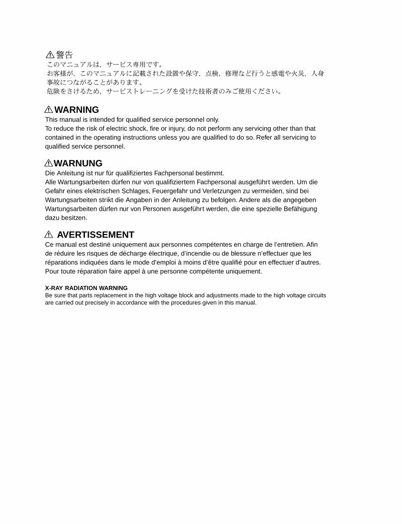
! WARNINGThis manual is intended for qualified service personnel only.To reduce the risk of electric shock, fire or injury, do not perform any servicing other than thatcontained in the operating instructions unless you are qualified to do so. Refer all servicing toqualified service personnel.
! WARNUNGDie Anleitung ist nur für qualifiziertes Fachpersonal bestimmt.Alle Wartungsarbeiten dürfen nur von qualifiziertem Fachpersonal ausgeführt werden. Um dieGefahr eines elektrischen Schlages, Feuergefahr und Verletzungen zu vermeiden, sind beiWartungsarbeiten strikt die Angaben in der Anleitung zu befolgen. Andere als die angegebenWartungsarbeiten dürfen nur von Personen ausgeführt werden, die eine spezielle Befähigungdazu besitzen.
! AVERTISSEMENTCe manual est destiné uniquement aux personnes compétentes en charge de l’entretien. Afinde réduire les risques de décharge électrique, d’incendie ou de blessure n’effectuer que lesréparations indiquées dans le mode d’emploi à moins d’être qualifié pour en effectuer d’autres.Pour toute réparation faire appel à une personne compétente uniquement.
X-RAY RADIATION WARNINGBe sure that parts replacement in the high voltage block and adjustments made to the high voltage circuitsare carried out precisely in accordance with the procedures given in this manual.

BVF-10 (UCJ)
BVF-10CE (CE)1 (E)
Table of Contents
1. Service Overview
1-1. Notes on Repair Parts .............................................................................1-1(E)
1-2. Location of Printed Circuit Boards ........................................................1-1(E)
1-3. Recommended Replacement Parts .........................................................1-1(E)
1-4. Connector Input/Output Signals .............................................................1-2(E)
1-5. Disconnecting/Connecting Flexible Card Wire .....................................1-2(E)
1-6. Cleaning .................................................................................................1-3(E)1-6-1. Cleaning of Viewfinder .........................................................1-3(E)1-6-2. Cares After Using at Special Environment ...........................1-3(E)
1-7. Replacement of CRT ..............................................................................1-4(E)
2. Electrical Alignment
2-1. Electrical Adjustment Using a Camera ..................................................2-1(E)2-1-1. Notes on adjustment ..............................................................2-1(E)2-1-2. Equipment/Fixtures ...............................................................2-1(E)2-1-3. Connections ...........................................................................2-1(E)2-1-4. Initial Setting .........................................................................2-1(E)2-1-5. Extending Viewfinder ...........................................................2-2(E)2-1-6. Vertical Hold Adjustment .....................................................2-2(E)2-1-7. Horizontal Hold Adjustment .................................................2-3(E)2-1-8. Bright Set Adjustment ...........................................................2-3(E)2-1-9. Focus Adjustment..................................................................2-4(E)2-1-10. Heater Voltage Adjustment ...................................................2-4(E)2-1-11. Picture Frame Adjustment.....................................................2-5(E)
2-2. Electrical Adjustment Using a VF Checker ...........................................2-6(E)2-2-1. Notes on Adjustment .............................................................2-6(E)2-2-2. Equipment/Fixtures ...............................................................2-6(E)2-2-3. Connections ...........................................................................2-7(E)2-2-4. Settings for adjustment ..........................................................2-7(E)2-2-5. Extending Viewfinder ...........................................................2-7(E)2-2-6. Vertical Hold Adjustment .....................................................2-8(E)2-2-7. Horizontal Hold Adjustment .................................................2-8(E)2-2-8. Bright Set Adjustment ...........................................................2-9(E)2-2-9. Focus Adjustment..................................................................2-9(E)2-2-10. Heater Voltage Adjustment .................................................2-10(E)2-2-11. Picture Frame Adjustment...................................................2-10(E)
2 (E) BVF-10 (UCJ)
BVF-10CE (CE)
3. Spare Parts
3-1. Notes on Repair Parts .................................................................................. 3-1
3-2. Exploded Views .......................................................................................... 3-2
3-3. Electrical Parts List ..................................................................................... 3-4
3-4. Supplied Accessories .................................................................................. 3-7
3-5. Optional Fixtures ......................................................................................... 3-7
4. Semiconductor Pin Assignments
5. Diagrams and Board Layouts
1-1 (E)BVF-10 (UCJ)
BVF-10CE (CE)
Section 1Service Overview
1-1. Notes on Repair Parts
1. wwwwwSafety Related Components WarningComponents marked ! are critical to safe operation.Therefore, specified parts should be used in the case ofreplacement.
2. Standardization of PartsSome repair parts supplied by Sony differ from thoseused for the unit. These are because of parts common-ality and improvement.Parts list has the present standardized repair parts.
3. Stock of PartsParts marked with “o” at SP(Supply Code) column ofthe spare parts list may be not stocked. Therefore, thedelivery date will be delayed.
4. Units RepresentationThe following represented units are changed oromitted in writing.
Units Representation
Capacitance µF uF
Inductance µH uH
Resistance Ω Abbreviation
5. Destination RepresentationThe part indicated “For UCJ/CE” in the spare parts listis used in the unit written below.For UCJ : The part is used in a unit for Japan, U.S.A.
and Canada.For CE : The part is used in a unit for regions except
the above countries.
1-2. Location of Printed Circuit Boards
1-3. Recommended Replacement Parts
Parts listed below are recommended replacement parts.They are subject to cracks with the lapse of time. Checksometimes by visual, and replace as necessary.
No. Description Sony P/N
1 WIND SCREEN 3-709-096-0X*1
3-708-875-0X*2
2 MIC CUSHION, RUBBER 3-692-138-0X
3 EYE CUP 3-723-079-0X*3
4 SPACER, MICROPHONE 3-179-882-0X
*1: Serial No.10401 and higher (UCJ)Serial No.40401 and higher (CE)
*2: Serial No.10001 through 10400 (UCJ)Serial No.40001 through 40400 (CE)
*3: It is recommended that the MIC cushions are replaced in pairs. In thiscase, please order two pieces.
VR-199
LP-84
LP-85VF-60
3
2
1 4

1-2 (E) BVF-10 (UCJ)
BVF-10CE (CE)
1-4. Connector Input/Output Signals
VF (20P MALE)
(External View)
Pin No. Signal I/O Specifications
1 VTR SAVE IND IN GND:Indicator lightsOPEN:Indicator goes out
2 ABNORMAL IND IN GND:Indicator lightsOPEN:Indicator goes out
3 16:9 MODE IN GND:16:9OPEN:4:3
4 REC (L) IND IN 9 V:Indicator lightsGND or OPEN:Indicator goes out
5 NC
6 CCIR/EIA IN 9.3 V:CCIRGND:EIA
7 DISPLAY OUT ON:OPENOFF:GND
8 G TALLY IN 5 V:Indicator lightsGND or OPEN:Indicator goes out
9 NC
10 NC
11 ZEBRA OUT ON:GNDOFF:5 V
12 VF VIDEO (X) IN 1.0 V p-pZi = 75 Z
13 NC
14 NC
15 NC
16 BATT IND IN 5 V:Indicator lightsGND or OPEN:Indicator goes out
17 TALLY IND IN 9 V:Indicator lightsGND or OPEN:Indicator goes out
18 + 9.3 V(VF) IN REG + 9.3 V
19 GND GND
20 NC
This unit normally operates with the above input signals.Cameras described in this manual can output the signalssatisfying the specifications.
1-5. Disconnecting/Connecting FlexibleCard Wire
The flexible card wire is used between the VF-60 and VR-199 boards. Take care not to break this flexible card wire.This shorten the wire life.
Disconnecting
1. Turn off the power.2. Slide portions A in the direciton of the arrow to unlock
and pull out the flexible card wire.
Connecting
m• Be careful not to insert the flexible card wire obliquely.• Check that the conductive surface of the flexible card
wire is not soiled with dust.
1. Slide portions A in the direction of the arrow andinsert the flexible card wire as far as it will go with theconductive surface down.
2. Slide portions A in the reverse direction to lock.
1-4. Connector Input/Output Signals1-5. Disconnecting/Connecting Flexible Card Wire
A
Conductive surface
A

1-3 (E)BVF-10 (UCJ)
BVF-10CE (CE)
1-6. Cleaning
1-6-1. Cleaning of Viewfinder
By extracting VF tube sub assy, lens and MC protector canbe easily cleaned. And also dust on the CRT surface ormirror can be easily cleaned off.
1. Turn the hold ring to the left and extract the VF tubesub assy.
2. Detach the eyecup.3. Remove the MC protector with a commercially
available camera lens cleaner. Blow off dust with ablower carefully so as not to flaw the mirror.
5. After the cleaning is completed, install by reversingthe preceding steps. Align red lines of the VF tube andVF tube sub assy when inserting, and turn the holdring to the right until it locks.
m. Do not use any type of solvent, such as alcohol, benzine
or thinner to remove stains.. Be sure to attach the eyecup to the VF, or the MC
protector may come off.. To protect the viewfinder lens from drops, put the MC
protector in the filter holder and attach the eyecupsecurely.
1-6-2. Cares After Using at SpecialEnvironment
It is recommended to check the following items aftergathering the news at seaside, dust area or spa.
1. Clean off sand and other dust in the unit carefully.2. Do not allow salt in seawater or sulfur in spa to contact
a not-painted surface of the cabinet. They may cause tocorrode. Clean with alcohol immediately if contacted.
3. Clean the connection surface of connectors.4. Carry out the common operation check and check that
the unit has not an abnormal sound or operation.
Hold ring
VF tube sub assembly
Align red lines
MC protector
Filter holder
Eyecup
1-6. Cleaning

1-4 (E) BVF-10 (UCJ)
BVF-10CE (CE)
7. Remove the three screws and remove the CRT fromthe VF tube assembly.
8. Remove the CRT tube from the CRT.
9. Remove the four screws and remove the mask spacer.10. Disconnect the connectors CN21 on LP-84 board and
CN31 on LP-85 board.
11. Install a new CRT in the reverse procedures ofremoval.
12. Referring to Section 2 “Electrical Alignment”, be sureto perform the adjustments.nWhen installing the upper chassis, take care not toclamp the harness between upper and lower chassis.
1-7. Replacement of CRT
1-7. Replacement of CRT
1. Loosen the screw of the MIC clamp and open the MICclamp.
2. Remove the two screws (K2.6 x 5).3. Remove the three hexagonal socket bolts and remove
the upper chassis.
4. Disconnect the flexible card wire CN11 of the VR-119board.
5. Disconnect the four connectors CN2, CN4 and anodecable of the VF-60 board.
6. Detach a tape and remove the CRT socket from theCRT.
MIC clamp
Upper chassis
BOLT,HEXAGON SOCKETS 2.6 x 6
K 2.6 x 5
Anode cable CRT socket
CRT
CN4
VF-60CN2
CRT
PTP2.6 x 8
Lug
VF Tube assembly
PTP2.6 x 8PTP2 x 6
Mask spacer
LP-84
CRT
CN21
CN31 LP-85
K2 x 5
K2 x 5

2-1 (E)BVF-10 (UCJ)
BVF-10CE (CE)
2-1-3. Connections
2-1-4. Initial Setting
Setup menu:. Execute the Scene File Standard.
MENU : PaintPAGE : Scene File (P8)ITEM : Standard
Press the MENU SEL switch (on the front panel) toexecute the Scene File Standard.
. Set each item through the setup menu as follows.(Refer to the Operation Manual to operate the setupmenu.)MENU : Operation
PAGE : Gain Sw (?3)ITEM : Low → 0 dBITEM : Middle → 9 dBITEM : High → 18 dB
Side Panel:VTR SAVE/STBY switch → STBYGAIN switch → L (0 dB)OUTPUT/DCC switch → CAM/OFFWHITE BAL switch → PRST
Front Panel:SHUTTER switch → OFF
2-1. Electrical Adjustment Using aCamera
2-1-1. Notes on adjustment
1. When performing adjustment, read throughly thefollowing comments.
. The calibration of all measuring equipment should becompleted.
. Peripheral equipment (camera, and others) alignmentshould be completed.
. “2-1-4. Settings for adjustment” should be completed.
. Turn off the power before extending the plug-in boardusing the extension board.
wThere is a danger of an electric shock around the CRT dueto high voltage. Therefore, do not touch the CRT.Be very careful when service in a live.
2-1-2. Equipment/Fixtures
. Color video camera BVP-550
. CCD unit OHB-450/550 series
. Camera adaptor CA-550/550P
. AC adaptorAC-550/550CE or equivalent
. OscilloscopeTektronix 2465B or equivalent
. Waveform monitorTektronix 1750/1751 or equivalent
. B/W monitor
. Digital voltmeter
. Frequency counter
Fixtures Sony P/N
Pattern box “PTB-500” J-6026-140-B
Resolution chart (4:3) J-6026-100-A
Resolution chart (16:9) J-6394-320-A
VF extension harness J-6395-050-A
CCD UNITOHB
ENG/EFP LENS
1.5" VFBVF-10/10CE
COLOR VIDEO CAMERABVP-550
CAMERA ADAPTORCA-550/550P
A-ch
75Ω
PATTERNBOX
AC ADAPTORAC-550/550CE
TESTOUT
Waveform monitor
Section 2Electrical Alignment

2-2 (E) BVF-10 (UCJ)
BVF-10CE (CE)
2-1-6. Vertical Hold Adjustment
Equipment : Frequency counter
Preparations:Extend the IF-510 board of BVP-550 with EX-464 exten-sion board.Short between pins 45 and 92 on the EX-464 board using ashorting clip.Set 1RV6 (V SIZE)/VF-60 board to the mechanical centerposition.(When 1RV6 is marked, it should not be turned.)
Test point : TP3/VF-60GND : E1/VF-60
Adjustment point : 1RV5 (V HOLD)/VF-60Specifications : 48.0 ±0.5 Hz (for NTSC)
38.0 ±0.5 Hz (for PAL)
After adjustment is completed, disconnect the shorting clipon the EX-464.Connect the IF-510 board to the camera.
51
RV3
RV4
RV5 RV9 RV8
TP5
CN2TP4
CN5
RV1
RV2TP1
CN1TP2RV6RV10RV7
TP3 CN4
E1
VF-60 BOARD (A SIDE)
2-1-5. Extending Viewfinder
1. Turn off the main power switch (on the camera) beforeperforming adjustment.
2. Remove the viewfinder from the camera, then removethe chassis (upper). (Refer to Section 1-7“Replacementof CRT”.)
3. Connect the viewfinder to the camera using the VFextension harness (J-6395-050-A).
4. Turn on the main power switch.
MIC clamp
Upper chassis
2-1. Electrical Adjustment Using a Camera
2-3 (E)BVF-10 (UCJ)
BVF-10CE (CE)
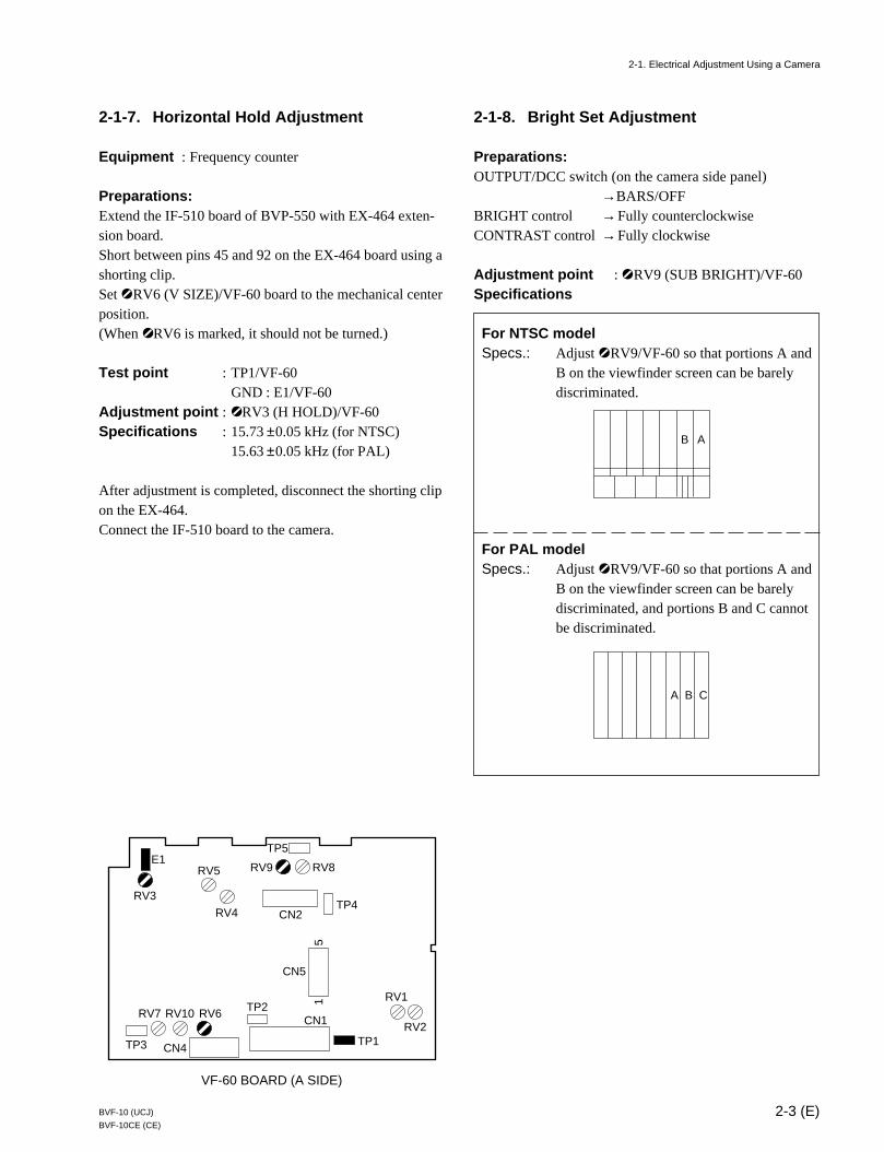
2-1-7. Horizontal Hold Adjustment
Equipment : Frequency counter
Preparations:Extend the IF-510 board of BVP-550 with EX-464 exten-sion board.Short between pins 45 and 92 on the EX-464 board using ashorting clip.Set 1RV6 (V SIZE)/VF-60 board to the mechanical centerposition.(When 1RV6 is marked, it should not be turned.)
Test point : TP1/VF-60GND : E1/VF-60
Adjustment point : 1RV3 (H HOLD)/VF-60Specifications : 15.73 ±0.05 kHz (for NTSC)
15.63 ±0.05 kHz (for PAL)
After adjustment is completed, disconnect the shorting clipon the EX-464.Connect the IF-510 board to the camera.
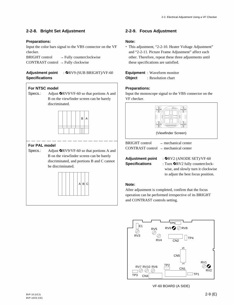
2-1-8. Bright Set Adjustment
Preparations:OUTPUT/DCC switch (on the camera side panel)
→BARS/OFFBRIGHT control →Fully counterclockwiseCONTRAST control→Fully clockwise
Adjustment point : 1RV9 (SUB BRIGHT)/VF-60Specifications
For NTSC modelSpecs.: Adjust 1RV9/VF-60 so that portions A and
B on the viewfinder screen can be barelydiscriminated.
For PAL modelSpecs.: Adjust 1RV9/VF-60 so that portions A and
B on the viewfinder screen can be barelydiscriminated, and portions B and C cannotbe discriminated.
51
RV3
RV4
RV5 RV9 RV8
TP5
CN2TP4
CN5
RV1
RV2TP1
CN1TP2RV6RV10RV7
TP3 CN4
E1
VF-60 BOARD (A SIDE)
2-1. Electrical Adjustment Using a Camera
AB
A B C
2-4 (E) BVF-10 (UCJ)
BVF-10CE (CE)
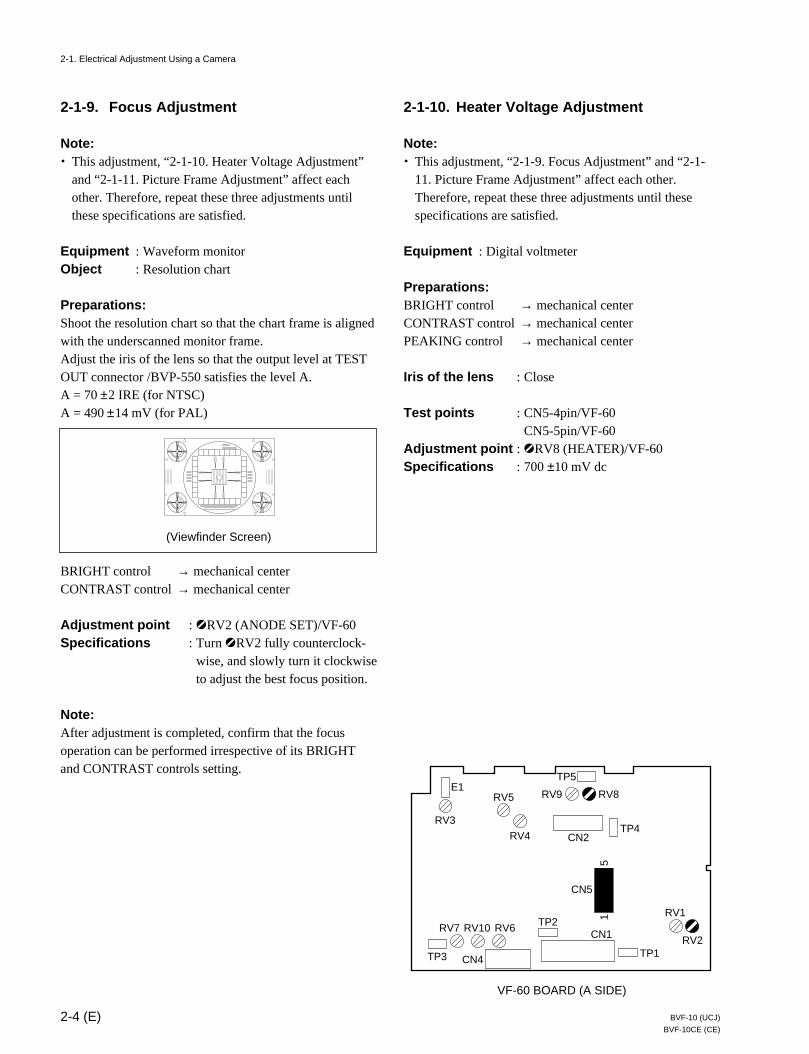
2-1-9. Focus Adjustment
Note:. This adjustment, “2-1-10. Heater Voltage Adjustment”
and “2-1-11. Picture Frame Adjustment” affect eachother. Therefore, repeat these three adjustments untilthese specifications are satisfied.
Equipment : Waveform monitorObject : Resolution chart
Preparations:Shoot the resolution chart so that the chart frame is alignedwith the underscanned monitor frame.Adjust the iris of the lens so that the output level at TESTOUT connector /BVP-550 satisfies the level A.A = 70 ±2 IRE (for NTSC)A = 490 ±14 mV (for PAL)
(Viewfinder Screen)
BRIGHT control → mechanical centerCONTRAST control→ mechanical center
Adjustment point : 1RV2 (ANODE SET)/VF-60Specifications : Turn 1RV2 fully counterclock-
wise, and slowly turn it clockwiseto adjust the best focus position.
Note:After adjustment is completed, confirm that the focusoperation can be performed irrespective of its BRIGHTand CONTRAST controls setting.
2-1-10. Heater Voltage Adjustment
Note:. This adjustment, “2-1-9. Focus Adjustment” and “2-1-
11. Picture Frame Adjustment” affect each other.Therefore, repeat these three adjustments until thesespecifications are satisfied.
Equipment : Digital voltmeter
Preparations:BRIGHT control → mechanical centerCONTRAST control→ mechanical centerPEAKING control → mechanical center
Iris of the lens : Close
Test points : CN5-4pin/VF-60CN5-5pin/VF-60
Adjustment point : 1RV8 (HEATER)/VF-60Specifications : 700 ±10 mV dc
51
RV3
RV4
RV5 RV9 RV8
TP5
CN2TP4
CN5
RV1
RV2TP1
CN1TP2RV6RV10RV7
TP3 CN4
E1
VF-60 BOARD (A SIDE)
2-1. Electrical Adjustment Using a Camera
2-5 (E)BVF-10 (UCJ)
BVF-10CE (CE)
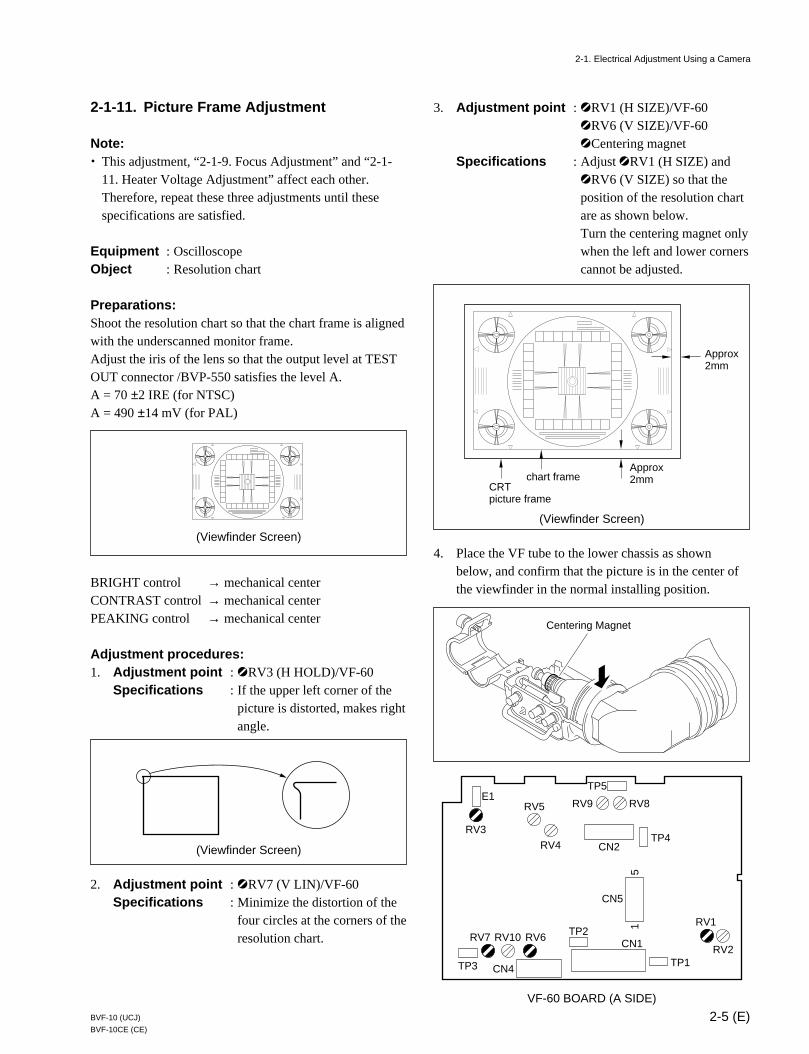
3. Adjustment point : 1RV1 (H SIZE)/VF-601RV6 (V SIZE)/VF-601Centering magnet
Specifications : Adjust 1RV1 (H SIZE) and1RV6 (V SIZE) so that theposition of the resolution chartare as shown below.Turn the centering magnet onlywhen the left and lower cornerscannot be adjusted.
(Viewfinder Screen)
4. Place the VF tube to the lower chassis as shownbelow, and confirm that the picture is in the center ofthe viewfinder in the normal installing position.
Centering Magnet5
1
RV3
RV4
RV5 RV9 RV8
TP5
CN2TP4
CN5
RV1
RV2TP1
CN1TP2RV6RV10RV7
TP3 CN4
E1
VF-60 BOARD (A SIDE)
Vewfinder Screen
CRT picture frame
chart frameApprox 2mm
Approx 2mm
2-1. Electrical Adjustment Using a Camera
2-1-11. Picture Frame Adjustment
Note:. This adjustment, “2-1-9. Focus Adjustment” and “2-1-
11. Heater Voltage Adjustment” affect each other.Therefore, repeat these three adjustments until thesespecifications are satisfied.
Equipment : OscilloscopeObject : Resolution chart
Preparations:Shoot the resolution chart so that the chart frame is alignedwith the underscanned monitor frame.Adjust the iris of the lens so that the output level at TESTOUT connector /BVP-550 satisfies the level A.A = 70 ±2 IRE (for NTSC)A = 490 ±14 mV (for PAL)
(Viewfinder Screen)
BRIGHT control → mechanical centerCONTRAST control→ mechanical centerPEAKING control → mechanical center
Adjustment procedures:1. Adjustment point : 1RV3 (H HOLD)/VF-60
Specifications : If the upper left corner of thepicture is distorted, makes rightangle.
(Viewfinder Screen)
2. Adjustment point : 1RV7 (V LIN)/VF-60Specifications : Minimize the distortion of the
four circles at the corners of theresolution chart.

2-6 (E) BVF-10 (UCJ)
BVF-10CE (CE)
5. Test point : TP3/VF-60GND : E1/VF-60
Measure and memorize the level A shown in the figurebelow.
(Oscilloscope)
6. Extend the AT-95 board of BVP-550 using EX-464extension board, and short between pins 76 and 100 onthe EX-464 board using a shorting clip. (Turn into16:9 mode.)
7. Test point :TP3/VF-60GND : E1/VF-60
Adjustment point :1RV10 (V SIZE (WIDE))/VF-60Specifications :Measure the level B, and adjust
the ratio to A : B = 4 : 3.
(Oscilloscope)
Notes:. When the centering magnet is turned, paint-lock it again.. After these adjustments are completed, disconnect the
shorting clip, and connect the AT-95 board to thecamera.
51
RV3
RV4
RV5 RV9 RV8
TP5
CN2TP4
CN5
RV1
RV2TP1
CN1TP2RV6RV10RV7
TP3 CN4
E1
VF-60 BOARD (A SIDE)
2-1. Electrical Adjustment Using a Camera2-2. Electrical Adjustment Using a VF Checker
A
B
2-2. Electrical Adjustment Using a VFChecker
2-2-1. Notes on Adjustment
1. When performing adjustment, read throughly thefollowing comments.
. The calibration of all measuring equipment should becompleted.
. “2-2-4. Setting for adjustment” should be completed.
wThere is a danger of an electric shock around the CRT dueto high voltage. Therefore, do not touch the CRT.Be very careful when service in a live.
2-2-2. Equipment/Fixtures
. Composite signal generatorShibasoku TG21AX or equivalent
. Monoscope signal output unitShibasoku TG21A1001 or equivalent [For NTSC]Shibasoku TG21A2001 or equivalent [For PAL]
. AC adapterSony AC-550 or equivalent
. OscilloscopeTektronix 2465B or equivalent
. Waveform monitorTektronix 1750/1751 or equivalent
. Frequency counter
Fixtures Sony P/N
VF cheker J-6422-300-A
VF extension harness J-6395-050-A

2-7 (E)BVF-10 (UCJ)
BVF-10CE (CE)
2-2-3. Connections
2-2-4. Settings for adjustment
Set switches as follows before adjustment.
VF checker:INPUT VIDEO VBS switch → SGINPUT VIDEO Y/R-Y/B-Y switch → SGEIA/CCIR switch → EIA [For NTSC]EIA/CCIR switch → CCIR [For PAL]16 : 9/4 : 3 switch → 4 : 3COMP/VBS switch → VBS
Signal generator
VF BVF-10 AC ADAPTOR
AC-550
INPUT VIDEO (VBS,Y,R-Y,B-Y)
EXT DC
VF
VF checker
2-2. Electrical Adjustment Using a VF Checker
2-2-5. Extending Viewfinder
1. Turn off the main power switch (on the camera) beforeperforming adjustment.
2. Remove the chassis (upper). (Refer to Section 1-7“Replacement of CRT”.)
3. Connect the viewfinder to the camera using the VFextension harness (J-6395-050-A).
4. Turn on the main power switch.
MIC clamp
Upper chassis
2-8 (E) BVF-10 (UCJ)
BVF-10CE (CE)
2-2. Electrical Adjustment Using a VF Checker
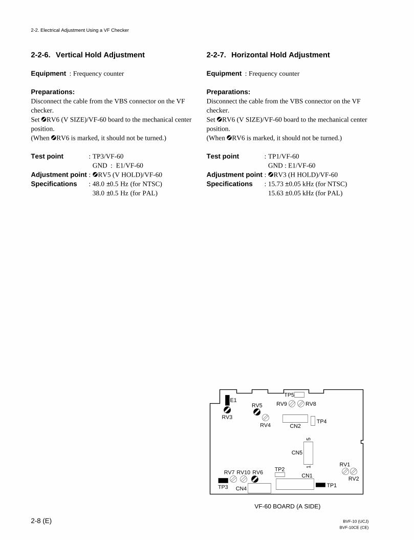
2-2-6. Vertical Hold Adjustment
Equipment : Frequency counter
Preparations:Disconnect the cable from the VBS connector on the VFchecker.Set 1RV6 (V SIZE)/VF-60 board to the mechanical centerposition.(When 1RV6 is marked, it should not be turned.)
Test point : TP3/VF-60GND : E1/VF-60
Adjustment point : 1RV5 (V HOLD)/VF-60Specifications : 48.0 ±0.5 Hz (for NTSC)
38.0 ±0.5 Hz (for PAL)
2-2-7. Horizontal Hold Adjustment
Equipment : Frequency counter
Preparations:Disconnect the cable from the VBS connector on the VFchecker.Set 1RV6 (V SIZE)/VF-60 board to the mechanical centerposition.(When 1RV6 is marked, it should not be turned.)
Test point : TP1/VF-60GND : E1/VF-60
Adjustment point : 1RV3 (H HOLD)/VF-60Specifications : 15.73 ±0.05 kHz (for NTSC)
15.63 ±0.05 kHz (for PAL)
51
RV3
RV4
RV5 RV9 RV8
TP5
CN2TP4
CN5
RV1
RV2TP1
CN1TP2RV6RV10RV7
TP3 CN4
E1
VF-60 BOARD (A SIDE)
2-9 (E)BVF-10 (UCJ)
BVF-10CE (CE)
2-2. Electrical Adjustment Using a VF Checker
2-2-8. Bright Set Adjustment
Preparations:Input the color bars signal to the VBS connector on the VFchecker.BRIGHT control → Fully counterclockwiseCONTRAST control→ Fully clockwise
Adjustment point : 1RV9 (SUB BRIGHT)/VF-60Specifications
For NTSC modelSpecs.: Adjust 1RV9/VF-60 so that portions A and
B on the viewfinder screen can be barelydiscriminated.
For PAL modelSpecs.: Adjust 1RV9/VF-60 so that portions A and
B on the viewfinder screen can be barelydiscriminated, and portions B and C cannotbe discriminated.
A B C
AB
2-2-9. Focus Adjustment
Note:. This adjustment, “2-2-10. Heater Voltage Adjustment”
and “2-2-11. Picture Frame Adjustment” affect eachother. Therefore, repeat these three adjustments untilthese specifications are satisfied.
Equipment : Waveform monitorObject : Resolution chart
Preparations:Input the monoscope signal to the VBS connector on theVF checker.
(Viewfinder Screen)
BRIGHT control → mechanical centerCONTRAST control→ mechanical center
Adjustment point : 1RV2 (ANODE SET)/VF-60Specifications : Turn 1RV2 fully counterclock-
wise, and slowly turn it clockwiseto adjust the best focus position.
Note:After adjustment is completed, confirm that the focusoperation can be performed irrespective of its BRIGHTand CONTRAST controls setting.
51
RV3
RV4
RV5 RV9 RV8
TP5
CN2TP4
CN5
RV1
RV2TP1
CN1TP2RV6RV10RV7
TP3 CN4
E1
VF-60 BOARD (A SIDE)

2-10 (E) BVF-10 (UCJ)
BVF-10CE (CE)
2-2. Electrical Adjustment Using a VF Checker
2-2-10. Heater Voltage Adjustment
Note:. This adjustment, “2-2-9. Focus Adjustment” and “2-2-
11. Picture Frame Adjustment” affect each other.Therefore, repeat these three adjustments until thesespecifications are satisfied.
Equipment : Digital voltmeter
Preparations:BRIGHT control → mechanical centerCONTRAST control→ mechanical centerPEAKING control → mechanical center
Setting of the signal generator (TG21A1001)LUMINANCE → OFFCHROMINANCE → OFF(Or input the black burst signal using another signalgenerator.)
Test points : CN5-4pin/VF-60CN5-5pin/VF-60
Adjustment point : 1RV8 (HEATER)/VF-60Specifications : 700 ±10 mV dc
51
RV3
RV4
RV5 RV9 RV8
TP5
CN2TP4
CN5
RV1
RV2TP1
CN1TP2RV6RV10RV7
TP3 CN4
E1
VF-60 BOARD (A SIDE)
2-2-11. Picture Frame Adjustment
Note:. This adjustment, “2-2-9. Focus Adjustment” and “2-2-
10. Heater Voltage Adjustment” affect each other.Therefore, repeat these three adjustments until thesespecifications are satisfied.
Equipment : OscilloscopeObject : Resolution chart
Preparations:Input the monoscope signal to the VBS connector on theVF checker.
(Viewfinder Screen)
BRIGHT control → mechanical centerCONTRAST control→ mechanical centerPEAKING control → mechanical center
Adjustment procedures:1. Adjustment point : 1RV3 (H HOLD)/VF-60
Specifications : If the upper left corner of thepicture is distorted, makes rightangle.
(Viewfinder Screen)
2. Adjustment point : 1RV7 (V LIN)/VF-60Specifications : Minimize the distortion of the
four circles at the corners of theresolution chart.
2-11 (E)BVF-10 (UCJ)
BVF-10CE (CE)
2-2. Electrical Adjustment Using a VF Checker
3. Adjustment point : 1RV1 (H SIZE)/VF-601RV6 (V SIZE)/VF-601Centering magnet
Specifications : Adjust 1RV1 (H SIZE) and1RV6 (V SIZE) so that theposition of the resolution chartare as shown below.Turn the centering magnet onlywhen the left and lower cornerscannot be adjusted.
(Viewfinder Screen)
4. Place the VF tube to the lower chassis as shownbelow, and confirm that the picture is in the center ofthe viewfinder in the normal installing position.
5. Test point : TP3/VF-60GND : E1/VF-60
Measure and memorize the level A shown in the figurebelow.
(Oscilloscope)
Vewfinder Screen
CRT picture frame
chart frameApprox 2mm
Approx 2mm
51
RV3
RV4
RV5 RV9 RV8
TP5
CN2TP4
CN5
RV1
RV2TP1
CN1TP2RV6RV10RV7
TP3 CN4
E1
VF-60 BOARD (A SIDE)
Centering Magnet
A
6. 16 : 9/4 : 3 switch/VF checker → 16 : 97. Test point : TP3/VF-60
GND : E1/VF-60Adjustment point : 1RV10 (V SIZE (WIDE))/VF-60Specifications : Measure the level B, and adjust
the ratio to A : B = 4 : 3.
(Oscilloscope)
Notes:. When the centering magnet is turned, paint-lock it again.. 16 : 9/4 : 3 switch/VF checker → 4 : 3
B

3-1BVF-10 (UCJ)
BVF-10CE (CE)
3-1. Notes on Repair Parts
1. w w w w w Safety Related Components WarningComponents marked ! are critical to safe operation. Therefore, specified parts should be used in thecase of replacement.
2. Standardization of PartsSome repair parts supplied by Sony differ from those used for the unit. These are because of partscommonality and improvement.Parts list has the present standardized repair parts.
3. Stock of PartsParts marked with “o” at SP (Supply Code) column of the spare parts list may be not stocked.Therefore, the delivery date will be delayed.
4. Units RepresentationThe following represented units are changed or omitted in writing.
Units Representation
Capacitance µF uF
Inductance µH uH
Resistance Ω Abbreviation
5. Destination RepresentationThe part indicated “For UCJ/CE” in the spare parts list is used in the unit written below.For UCJ : The part is used in a unit for Japan, U.S.A. and Canada.For CE : The part is used in a unit for regions except the above countries.
Section 3Spare Parts
3-2 BVF-10 (UCJ)
BVF-10CE (CE)
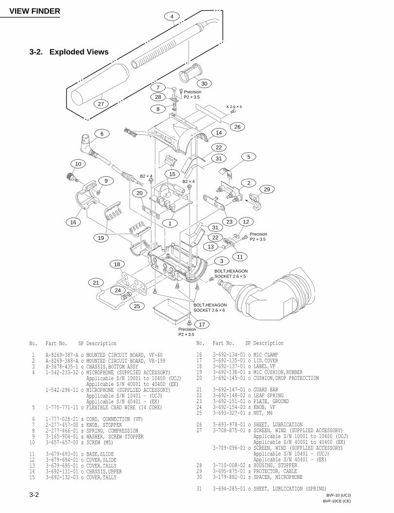
3-2. Exploded Views
VIEW FINDER
Precision P2 × 3.5
B2 × 4B2 × 4
Precision P2 × 3.5
BOLT,HEXAGON SOCKET 2.6 × 5
BOLT,HEXAGON SOCKET 2.6 × 6
7
28
8
22
14
2
5
23 12
22
13
3
17
25
2421
18
9
10
16
19
6
11
15
4
27
Precision P2 × 3.5
20
1
29
31
31
26
30
K 2.6 × 5
No. Part No. SP Description
1 A-8269-387-A o MOUNTED CIRCUIT BOARD, VF-60 2 A-8269-388-A o MOUNTED CIRCUIT BOARD, VR-199 3 X-3678-435-1 o CHASSIS,BOTTOM ASSY 4 1-542-233-12 o MICROPHONE (SUPPLIED ACCESSORY) Applicable S/N 10001 to 10400 (UCJ) Applicable S/N 40001 to 40400 (EK) 1-542-296-11 o MICROPHONE (SUPPLIED ACCESSORY) Applicable S/N 10401 - (UCJ) Applicable S/N 40401 - (EK) 5 1-775-771-11 o FLEXIBLE CARD WIRE (14 CORE)
6 1-777-028-21 s CORD, CONNECTION (VF) 7 2-277-457-00 s KNOB, STOPPER 8 2-277-466-01 s SPRING, COMPRESSION 9 3-165-904-01 s WASHER, SCREW STOPPER 10 3-657-657-00 s SCREW (M5)
11 3-679-693-01 o BASE,SLIDE 12 3-679-694-01 o COVER,SLIDE 13 3-679-695-01 o COVER,TALLY 14 3-692-131-01 o CHASSIS,UPPER 15 3-692-132-03 o COVER,TALLY
No. Part No. SP Description
16 3-692-134-01 o MIC CLAMP 17 3-692-135-01 o LID,COVER 18 3-692-137-01 o LABEL,VF 19 3-692-138-01 s MIC CUSHION,RUBBER 20 3-692-145-01 o CUSHION,DROP PROTECCTION
21 3-692-147-01 o GUARD BAR 22 3-692-148-02 o LEAF SPRING 23 3-692-151-01 o PLATE, GROUND 24 3-692-154-03 s KNOB, VF 25 3-693-327-01 s NUT, M6
26 3-693-978-01 o SHEET, LUBRICATION 27 3-708-875-01 s SCREEN, WIND (SUPPLIED ACCESSORY) Applicable S/N 10001 to 10400 (UCJ) Applicable S/N 40001 to 40400 (EK) 3-709-096-01 o SCREEN, WIND (SUPPLIED ACCESSORY) Applicable S/N 10401 - (UCJ) Applicable S/N 40401 - (EK) 28 3-710-008-02 s HOUSING, STOPPER 29 3-695-875-01 s PROTECTOR, CABLE 30 3-179-882-01 s SPACER, MICROPHONE
31 3-694-285-01 o SHEET, LUBLICATION (SPRING)

3-3BVF-10 (UCJ)
BVF-10CE (CE)
VIEW FINDER
No. Part No. SP Description
101 A-7612-389-B s TUBE SUB ASSY, VF 102 A-8269-389-A o MOUNTED CIRCUIT BOARD, LP-84 103 A-8269-390-A o MOUNTED CIRCUIT BOARD, LP-85 104 X-3722-436-1 o LENS ASSY 105 ! 1-251-386-11 s 1.5" CRT ASSY
106 3-176-022-03 o SPACER (B), MASK 107 3-176-414-01 o RETAINER, RING 108 3-335-207-01 s SHAFT, MOTOR 109 3-573-150-00 o SPRING, COMPRESSION 110 3-692-133-01 o RING,VF
111 3-692-136-02 o FIXED RING 112 3-692-139-01 o MIRROR(2) 113 3-692-144-01 o SPACER,LP 114 3-692-146-01 o HOLDER,MIRROR(2) 115 3-692-155-01 o PLATE,DISPLAY
116 3-692-166-04 o VF TUBE(3) 117 3-722-485-01 o ROLLER, SLIDE 118 3-723-069-02 o PROTECTOR, MC 119 3-723-073-01 o CUSHION, MIRROR 120 3-723-079-01 s EYE CUP
No. Part No. SP Description
121 3-725-220-02 o TUBE (A), CRT 122 3-725-276-01 s LUPE, VF 123 3-742-038-01 o NUT (2), PLATE 124 3-742-052-03 o HOLDER, EYE CUP 125 3-742-053-02 o RING
126 3-742-054-01 o TUBE 127 3-742-060-01 o HOLDER, RING 128 3-742-075-01 o HOLDER, FILTER
7-623-505-01 s LUG, 2 7-624-200-01 s NUT, PUSH 1.5 7-627-454-38 s SCREW, PRECISION +K 2.6X5 7-627-553-78 s SCREW,PRECISION +P 2X10 7-627-554-18 s SCREW,PRECISION +P 2X3.5 TYPE1
7-671-158-01 s BALL, STAINLESS (2.5 DIA) 7-682-545-04 s SCREW +B 3X4 7-683-412-05 s BOLT,HEXAGON SOCKET 2.6X6 7-685-104-19 s SCREW +P 2X6 TYPE2 NON-SLIT 7-685-134-19 s SCREW +P 2.6X8 TYPE2 NON-SLIT
P2.6 × 8
P2.6 × 8K2 × 5
K2 × 5
PTP2 × 6
P2 × 6
121
Precision P2 × 10
105
113102
106
115110
116
111
101
120
118
107
109
124128
107
109117
108
117
125
104
108122
126
123
123127
103
112
114
119
Precision P2 × 10
3-4 BVF-10 (UCJ)
BVF-10CE (CE)
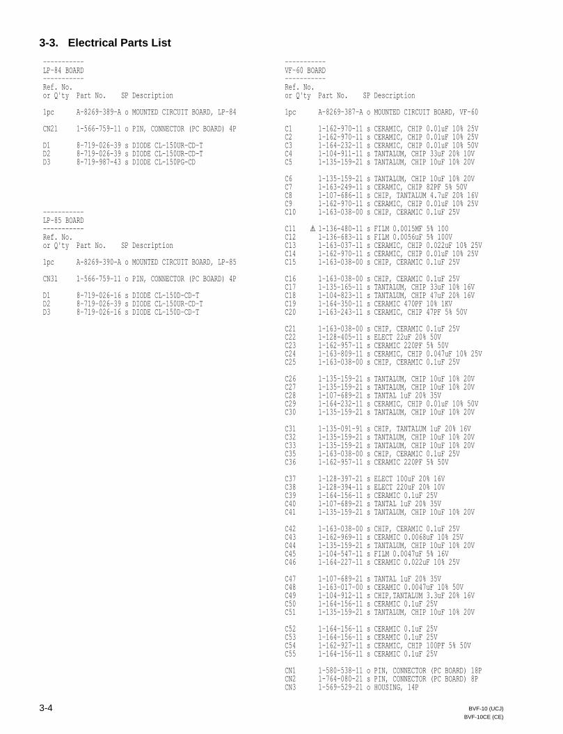
3-3. Electrical Parts List
----------- ----------- LP-84 BOARD VF-60 BOARD ----------- ----------- Ref. No. Ref. No. or Q'ty Part No. SP Description or Q'ty Part No. SP Description
1pc A-8269-389-A o MOUNTED CIRCUIT BOARD, LP-84 1pc A-8269-387-A o MOUNTED CIRCUIT BOARD, VF-60
CN21 1-566-759-11 o PIN, CONNECTOR (PC BOARD) 4P C1 1-162-970-11 s CERAMIC, CHIP 0.01uF 10% 25V C2 1-162-970-11 s CERAMIC, CHIP 0.01uF 10% 25V D1 8-719-026-39 s DIODE CL-150UR-CD-T C3 1-164-232-11 s CERAMIC, CHIP 0.01uF 10% 50V D2 8-719-026-39 s DIODE CL-150UR-CD-T C4 1-104-911-11 s TANTALUM, CHIP 33uF 20% 10V D3 8-719-987-43 s DIODE CL-150PG-CD C5 1-135-159-21 s TANTALUM, CHIP 10uF 10% 20V
C6 1-135-159-21 s TANTALUM, CHIP 10uF 10% 20V C7 1-163-249-11 s CERAMIC, CHIP 82PF 5% 50V C8 1-107-686-11 s CHIP, TANTALUM 4.7uF 20% 16V C9 1-162-970-11 s CERAMIC, CHIP 0.01uF 10% 25V ----------- C10 1-163-038-00 s CHIP, CERAMIC 0.1uF 25V LP-85 BOARD ----------- C11 ! 1-136-480-11 s FILM 0.0015MF 5% 100 Ref. No. C12 1-136-683-11 s FILM 0.0056uF 5% 100V or Q'ty Part No. SP Description C13 1-163-037-11 s CERAMIC, CHIP 0.022uF 10% 25V C14 1-162-970-11 s CERAMIC, CHIP 0.01uF 10% 25V 1pc A-8269-390-A o MOUNTED CIRCUIT BOARD, LP-85 C15 1-163-038-00 s CHIP, CERAMIC 0.1uF 25V
CN31 1-566-759-11 o PIN, CONNECTOR (PC BOARD) 4P C16 1-163-038-00 s CHIP, CERAMIC 0.1uF 25V C17 1-135-165-11 s TANTALUM, CHIP 33uF 10% 16V D1 8-719-026-16 s DIODE CL-150D-CD-T C18 1-104-823-11 s TANTALUM, CHIP 47uF 20% 16V D2 8-719-026-39 s DIODE CL-150UR-CD-T C19 1-164-350-11 s CERAMIC 470PF 10% 1KV D3 8-719-026-16 s DIODE CL-150D-CD-T C20 1-163-243-11 s CERAMIC, CHIP 47PF 5% 50V
C21 1-163-038-00 s CHIP, CERAMIC 0.1uF 25V C22 1-128-405-11 s ELECT 22uF 20% 50V C23 1-162-957-11 s CERAMIC 220PF 5% 50V C24 1-163-809-11 s CERAMIC, CHIP 0.047uF 10% 25V C25 1-163-038-00 s CHIP, CERAMIC 0.1uF 25V
C26 1-135-159-21 s TANTALUM, CHIP 10uF 10% 20V C27 1-135-159-21 s TANTALUM, CHIP 10uF 10% 20V C28 1-107-689-21 s TANTAL 1uF 20% 35V C29 1-164-232-11 s CERAMIC, CHIP 0.01uF 10% 50V C30 1-135-159-21 s TANTALUM, CHIP 10uF 10% 20V
C31 1-135-091-91 s CHIP, TANTALUM 1uF 20% 16V C32 1-135-159-21 s TANTALUM, CHIP 10uF 10% 20V C33 1-135-159-21 s TANTALUM, CHIP 10uF 10% 20V C35 1-163-038-00 s CHIP, CERAMIC 0.1uF 25V C36 1-162-957-11 s CERAMIC 220PF 5% 50V
C37 1-128-397-21 s ELECT 100uF 20% 16V C38 1-128-394-11 s ELECT 220uF 20% 10V C39 1-164-156-11 s CERAMIC 0.1uF 25V C40 1-107-689-21 s TANTAL 1uF 20% 35V C41 1-135-159-21 s TANTALUM, CHIP 10uF 10% 20V
C42 1-163-038-00 s CHIP, CERAMIC 0.1uF 25V C43 1-162-969-11 s CERAMIC 0.0068uF 10% 25V C44 1-135-159-21 s TANTALUM, CHIP 10uF 10% 20V C45 1-104-547-11 s FILM 0.0047uF 5% 16V C46 1-164-227-11 s CERAMIC 0.022uF 10% 25V
C47 1-107-689-21 s TANTAL 1uF 20% 35V C48 1-163-017-00 s CERAMIC 0.0047uF 10% 50V C49 1-104-912-11 s CHIP,TANTALUM 3.3uF 20% 16V C50 1-164-156-11 s CERAMIC 0.1uF 25V C51 1-135-159-21 s TANTALUM, CHIP 10uF 10% 20V
C52 1-164-156-11 s CERAMIC 0.1uF 25V C53 1-164-156-11 s CERAMIC 0.1uF 25V C54 1-162-927-11 s CERAMIC, CHIP 100PF 5% 50V C55 1-164-156-11 s CERAMIC 0.1uF 25V
CN1 1-580-538-11 o PIN, CONNECTOR (PC BOARD) 18P CN2 1-764-080-21 s PIN, CONNECTOR (PC BOARD) 8P CN3 1-569-529-21 o HOUSING, 14P

3-5BVF-10 (UCJ)
BVF-10CE (CE)
(VF-60 BOARD) (VF-60 BOARD)
Ref. No. Ref. No. or Q'ty Part No. SP Description or Q'ty Part No. SP Description
CN4 1-564-004-11 o PIN, CONNECTOR 5P R14 1-216-133-00 s CHIP, METAL 3.3M 5% 1/10W CN5 1-506-470-11 s PIN, CONNECTOR 5P R15 1-216-659-11 s METAL, CHIP 2.2K 0.5% 1/10W R16 1-208-774-11 s CHIP, METAL 470 0.50% 1/10W D1 8-719-404-35 s DIODE MA141WK R17 1-218-668-11 s CHIP, METAL 100 0.50% 1/16W D2 8-719-900-95 s DIODE V09G R18 1-216-666-11 s METAL, CHIP 4.3K 0.5% 1/10W D3 8-719-820-41 s DIODE 1SS302 D4 8-719-901-19 s DIODE V11N R19 1-218-680-11 s METAL 330 0.50% 1/16W D5 8-719-900-95 s DIODE V09G R20 1-218-700-11 s METAL 2.2K 0.50% 1/16W R21 1-218-700-11 s METAL 2.2K 0.50% 1/16W D6 8-719-404-35 s DIODE MA141WK R22 1-216-639-11 s METAL, CHIP 330 0.5% 1/10W D7 8-719-404-35 s DIODE MA141WK R23 1-218-724-11 s CHIP, METAL 22K 5% 1/16W D8 8-719-029-68 s DIODE RD6.2UJN-T1 D9 8-719-820-41 s DIODE 1SS302 R24 1-208-806-11 s CHIP, METAL 10K 0.50% 1/10W D10 8-719-404-35 s DIODE MA141WK R25 1-208-814-11 s CHIP, METAL 22K 0.50% 1/10W R26 1-216-133-00 s CHIP, METAL 3.3M 5% 1/10W D11 8-719-404-35 s DIODE MA141WK R27 1-216-673-11 s METAL, CHIP 8.2K 0.5% 1/10W D12 8-719-989-53 s DIODE CL-200HR-C-TSL R28 1-216-619-11 s CHIP, METAL 47 0.50% 1/10W
DL1 1-411-383-11 s DELAY LINE 80 nS R29 1-208-812-11 s CHIP, METAL 18K 0.50% 1/10W R30 1-208-824-11 s CHIP, METAL 56K 0.50% 1/10W IC1 ! 8-759-300-28 s IC HA11423MP R31 1-218-708-11 s METAL 4.7K 0.50% 1/16W IC2 8-759-100-94 s IC UPC358G2 R32 1-216-133-00 s CHIP, METAL 3.3M 5% 1/10W IC3 8-759-209-57 s IC TC4S69F R33 1-216-655-11 s CHIP, METAL 1.5K 0.50% 1/10W IC4 8-759-209-54 s IC TC4S01F R34 1-208-800-11 s CHIP, METAL 5.6K 0.50% 1/10W L2 ! 1-459-899-11 s COIL, HORIZONTAL LINEARITY R35 1-218-698-11 s METAL 1.8K 0.50% 1/16W L3 1-410-380-31 s INDUCTOR CHIP 8.2uH R36 1-216-687-11 s METAL, CHIP 33K 0.5% 1/10W R37 1-208-806-11 s CHIP, METAL 10K 0.50% 1/10W Q1 8-729-028-91 s TRANSISTOR DTA144EUA-T106 R38 1-218-714-11 s METAL 8.2K 0.50% 1/16W Q2 8-729-028-91 s TRANSISTOR DTA144EUA-T106 Q3 8-729-117-32 s TRANSISTOR 2SC4177 R39 1-216-633-11 s CHIP, METAL 180 0.50% 1/10W Q4 8-729-117-16 s TRANSISTOR 2SA1611-M6 R40 1-208-822-11 s CHIP, METAL 47K 0.50% 1/10W Q5 8-729-403-29 s TRANSISTOR XN6435 R41 1-216-609-11 s CHIP, METAL 18 0.50% 1/10W R42 1-218-724-11 s CHIP, METAL 22K 5% 1/16W Q6 8-729-024-56 s TRANSISTOR 2SA1808 R43 1-216-667-11 s METAL, CHIP 4.7K 0.5% 1/10W Q7 8-729-422-44 s TRANSISTOR 2SK663 Q8 8-729-403-32 s TRANSISTOR XN6534 R44 1-208-814-11 s CHIP, METAL 22K 0.50% 1/10W Q9 8-729-105-37 s TRANSISTOR 2SC3360-N16 R45 1-218-740-11 s METAL 100K 0.50% 1/16W Q10 8-729-105-37 s TRANSISTOR 2SC3360-N16 R46 1-216-673-11 s METAL, CHIP 8.2K 0.5% 1/10W R47 1-216-651-11 s METAL, CHIP 1K 0.5% 1/10W Q11 8-729-117-32 s TRANSISTOR 2SC4177 R48 1-218-899-11 s CHIP, METAL 150K 0.50% 1/16W Q12 8-729-117-16 s TRANSISTOR 2SA1611-M6 Q13 8-729-141-48 s TRANSISTOR 2SB624-BV345 R49 1-216-655-11 s CHIP, METAL 1.5K 0.50% 1/10W Q14 8-729-119-00 s TRANSISTOR 2SK612 R50 1-216-651-11 s METAL, CHIP 1K 0.5% 1/10W Q15 8-729-119-00 s TRANSISTOR 2SK612 R51 1-208-812-11 s CHIP, METAL 18K 0.50% 1/10W R52 1-208-814-11 s CHIP, METAL 22K 0.50% 1/10W Q16 8-729-028-91 s TRANSISTOR DTA144EUA-T106 R53 1-218-708-11 s METAL 4.7K 0.50% 1/16W Q17 8-729-117-32 s TRANSISTOR 2SC4177 Q18 8-729-117-16 s TRANSISTOR 2SA1611-M6 R54 1-216-667-11 s METAL, CHIP 4.7K 0.5% 1/10W Q19 8-729-117-32 s TRANSISTOR 2SC4177 R55 1-216-699-11 s CHIP, METAL 100K 0.50% 1/10W Q20 8-729-117-32 s TRANSISTOR 2SC4177 R56 1-216-133-00 s CHIP, METAL 3.3M 5% 1/10W R57 1-216-133-00 s CHIP, METAL 3.3M 5% 1/10W Q21 8-729-117-16 s TRANSISTOR 2SA1611-M6 R58 1-208-854-11 s CHIP,METAL 1M 0.50% 1/10W Q22 8-729-422-12 s TRANSISTOR 2SK664 R59 1-208-806-11 s CHIP, METAL 10K 0.50% 1/10W R1 1-216-671-11 s CHIP, METAL 6.8K 0.50% 1/10W R60 1-216-699-11 s CHIP, METAL 100K 0.50% 1/10W R2 1-216-309-00 s CHIP, METAL 5.6 5% 1/10W R61 1-216-133-00 s CHIP, METAL 3.3M 5% 1/10W R3 1-216-627-11 s CHIP, METAL 100 0.50% 1/10W R62 1-218-716-11 s METAL 10K 0.50% 1/16W R4 1-208-806-11 s CHIP, METAL 10K 0.50% 1/10W R63 1-216-677-11 s METAL, CHIP 12K 0.5% 1/10W R5 1-216-667-11 s METAL, CHIP 4.7K 0.5% 1/10W R64 1-218-768-11 s METAL 470K 0.50% 1/10W R6 1-208-774-11 s CHIP, METAL 470 0.50% 1/10W R65 1-216-685-11 s METAL, CHIP 27K 0.5% 1/10W R7 1-208-806-11 s CHIP, METAL 10K 0.50% 1/10W R66 1-216-687-11 s METAL, CHIP 33K 0.5% 1/10W R8 1-218-704-11 s METAL 3.3K 0.50% 1/16W R67 1-216-663-11 s METAL, CHIP 3.3K 0.5% 1/10W R9 1-216-635-11 s METAL, CHIP 220 0.5% 1/10W R68 1-218-648-11 s METAL 15 0.50% 1/16W R10 1-216-635-11 s METAL, CHIP 220 0.5% 1/10W R69 1-216-663-11 s METAL, CHIP 3.3K 0.5% 1/10W R11 1-218-680-11 s METAL 330 0.50% 1/16W R70 1-218-692-11 s CHIP, METAL 1K 0.50% 1/16W R12 1-216-611-11 s CHIP, METAL 22 0.50% 1/10W R71 1-216-673-11 s METAL, CHIP 8.2K 0.5% 1/10W R13 1-216-635-11 s METAL, CHIP 220 0.5% 1/10W R72 1-216-627-11 s CHIP, METAL 100 0.50% 1/10W

3-6 BVF-10 (UCJ)
BVF-10CE (CE)
------------ (VF-60 BOARD) VR-199 BOARD ------------ Ref. No. Ref. No. or Q'ty Part No. SP Description or Q'ty Part No. SP Description
R73 1-216-629-11 s CHIP, METAL 120 0.50% 1/10W 1pc A-8269-388-A o MOUNTED CIRCUIT BOARD, VR-199 R74 ! 1-218-883-11 s METAL 33K 0.50% 1/16W 1pc 3-692-151-01 o PLATE,GROUND R75 1-218-708-11 s METAL 4.7K 0.50% 1/16W R76 1-218-716-11 s METAL 10K 0.50% 1/16W C1 1-104-823-11 s TANTALUM, CHIP 47uF 20% 16V R77 1-208-814-11 s CHIP, METAL 22K 0.50% 1/10W C2 1-164-232-11 s CERAMIC, CHIP 0.01uF 10% 50V C3 1-164-232-11 s CERAMIC, CHIP 0.01uF 10% 50V R78 1-218-873-11 s CHIP, METAL 12K 0.50% 1/16W C4 1-163-037-11 s CERAMIC, CHIP 0.022uF 10% 25V R80 1-216-295-11 s CHIP, CONDUCTOR 0 C5 1-107-686-11 s CHIP, TANTALUM 4.7uF 20% 16V R81 1-218-716-11 s METAL 10K 0.50% 1/16W R82 1-216-793-11 s METAL 4.7 5% 1/16W C6 1-135-160-21 s CHIP, TANTALUM 15uF 10% 16V R83 1-218-716-11 s METAL 10K 0.50% 1/16W C7 1-163-038-00 s CHIP, CERAMIC 0.1uF 25V C8 1-164-232-11 s CERAMIC, CHIP 0.01uF 10% 50V R84 1-218-773-11 s CHIP, METAL 750K 0.50% 1/10W R85 1-218-841-11 s CHIP, METAL 560 0.50% 1/16W CN11 1-569-529-21 o HOUSING, 14P R86 1-216-659-11 s METAL, CHIP 2.2K 0.5% 1/10W R87 1-218-732-11 s METAL 47K 0.50% 1/16W D1 8-719-989-53 s DIODE CL-200HR-C-TSL R88 1-218-736-11 s METAL 68K 0.50% 1/16W D2 8-719-989-53 s DIODE CL-200HR-C-TSL
R89 1-218-732-11 s METAL 47K 0.50% 1/16W IC1 8-759-939-53 s IC BA225F-T2 R90 1-218-714-11 s METAL 8.2K 0.50% 1/16W R91 1-218-692-11 s CHIP, METAL 1K 0.50% 1/16W Q1 8-729-028-91 s TRANSISTOR DTA144EUA-T106 R92 1-218-883-11 s METAL 33K 0.50% 1/16W Q2 8-729-028-91 s TRANSISTOR DTA144EUA-T106 R93 1-218-867-11 s CHIP, METAL 6.8K 0.50% 1/16W Q3 8-729-402-19 s TRANSISTOR XN6501 Q4 8-729-402-19 s TRANSISTOR XN6501 R94 1-211-969-11 s CHIP, METAL 10 0.50% 1/16W R95 1-218-740-11 s METAL 100K 0.50% 1/16W R1 1-216-615-11 s METAL 33 0.50% 1/10W R96 ! 1-218-700-11 s METAL 2.2K 0.50% 1/16W R2 1-216-645-11 s METAL 560 0.50% 1/10W R97 1-218-710-11 s CHIP, METAL 5.6K 0.50% 1/16W R3 1-216-673-11 s METAL, CHIP 8.2K 0.5% 1/10W R98 1-218-740-11 s METAL 100K 0.50% 1/16W R4 1-208-814-11 s CHIP, METAL 22K 0.50% 1/10W R5 1-208-814-11 s CHIP, METAL 22K 0.50% 1/10W R99 1-218-684-11 s CHIP, METAL 470 0.50% 1/16W R100 1-218-684-11 s CHIP, METAL 470 0.50% 1/16W R6 1-208-814-11 s CHIP, METAL 22K 0.50% 1/10W R101 1-208-822-11 s CHIP, METAL 47K 0.50% 1/10W R7 1-218-772-11 s METAL 680K 0.50% 1/10W R102 1-216-659-11 s METAL, CHIP 2.2K 0.5% 1/10W R8 1-208-822-11 s CHIP, METAL 47K 0.50% 1/10W R103 1-218-752-11 s METAL 330K 0.50% 1/16W R9 1-208-824-11 s CHIP, METAL 56K 0.50% 1/10W R10 1-216-295-11 s CHIP, CONDUCTOR 0 R104 1-218-730-11 s CHIP, METAL 39K 0.50% 1/16W R105 1-218-883-11 s METAL 33K 0.50% 1/16W R11 1-208-822-11 s CHIP, METAL 47K 0.50% 1/10W R106 1-218-716-11 s METAL 10K 0.50% 1/16W R13 1-208-814-11 s CHIP, METAL 22K 0.50% 1/10W R14 1-208-774-11 s CHIP, METAL 470 0.50% 1/10W RV1 1-241-832-21 s RES, ADJ, METAL 5K R15 1-208-822-11 s CHIP, METAL 47K 0.50% 1/10W RV2 1-241-829-21 s RES, ADJ, METAL 1K R16 1-216-645-11 s METAL 560 0.50% 1/10W RV3 1-241-832-21 s RES, ADJ, METAL 5K RV4 1-241-838-11 s RES, ADJ, METAL 500K RV1 1-238-293-11 s CARBON, VAR 10K RV5 1-241-832-21 s RES, ADJ, METAL 5K RV2 1-238-290-11 s CARBON, VAR 1K RV3 1-238-296-11 s CARBON, VAR 10K RV6 1-241-828-21 s RES, ADJ, METAL 500 RV7 1-241-828-21 s RES, ADJ, METAL 500 RV8 1-241-825-11 s RES, ADJ, METAL 50 RV9 1-241-741-11 s RES, ADJ METAL 50K RV10 1-241-828-21 s RES, ADJ, METAL 500
S1 1-762-488-11 s SWITCH, TOGGLE S2 1-762-020-11 s SWITCH, TOGGLE S3 1-762-489-11 s SWITCH, TOGGLE
T1 ! 1-439-419-12 s TRANSFORMER, FLYBACK
VDR1 1-806-497-00 s VARISTOR ERZ-C05DK220

3-7BVF-10 (UCJ)
BVF-10CE (CE)
----- FRAME 3-4. Supplied Accessories ----- Ref. No. Ref. No. or Q'ty Part No. SP Description or Q'ty Part No. SP Description
! 1-251-386-11 s CRT ASSY, 1.5" 1pc 1-542-233-12 o MICROPHONE 1-775-771-11 o FLEXIBLE CARD WIRE (14 CORE) 1pc 3-179-882-01 o SPACER, MICROPHONE (VF-60 TO VR-199)
CN101 1-952-420-21 s HARNESS (VF CABLE3)
CN1F(to VF-60 BOARD) 1-580-585-11 o HOUSING, 18P 1-580-599-11 o CONTACT, FEMALE AWG26-30 3-5. Optional Fixtures CN2F(to VF-60 BOARD) 1-764-196-11 o HOUSING, 8P Part No. SP Description 1-695-215-11 o CONTACT, FEMALE AWG26-30 CN21F(to LP-84 BOARD) J-6026-100-A o RESOLUTION CHART 1-569-619-11 o HOUSING, CONNECTOR 4P J-6395-040-A o EXTENSION BOARD, EX-464 1-565-977-11 s CONTACT, FEMALE AWG 28-32 J-6395-050-A o VF EXTENSION HARNESS CN31F(to LP-85 BOARD) 1-569-619-11 o HOUSING, CONNECTOR 4P 1-565-977-11 s CONTACT, FEMALE AWG 28-32

4-1BVF-10 (UCJ)BVF-10CE (CE)
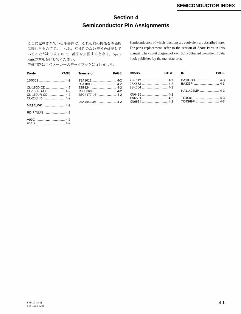
Section 4Semiconductor Pin Assignments
SEMICONDUCTOR INDEX
Semiconductors of which functions are equivalent are described here.
For parts replacement, refer to the section of Spare Parts in this
manual. The circuit diagram of each IC is obtained from the IC data
book published by the manufacturer.
Transistor PAGE
2SA1611 ........................... 4-22SA1808 ........................... 4-22SB624 ............................. 4-22SC3360 ........................... 4-22SC4177-L6 ...................... 4-2
DTA144EUA ...................... 4-2
Diode PAGE
1SS302 ............................. 4-2
CL-150D-CD ..................... 4-2CL-150PG-CD .................. 4-2CL-150UR-CD .................. 4-2CL-200HR ......................... 4-2
MA141WK ......................... 4-2
RD ? ?UJN ........................ 4-2
V09C ................................. 4-2V11 ? ................................. 4-2
IC PAGE
BA10358F ......................... 4-3BA225F ............................. 4-3
HA11423MP ..................... 4-3
TC4S01F .......................... 4-3TC4S69F .......................... 4-3
Others PAGE
2SK612 ............................. 4-22SK663 ............................. 4-22SK664 ............................. 4-2
XN6435 ............................. 4-2XN6501 ............................. 4-2XN6534 ............................. 4-2
4-2 BVF-10 (UCJ)BVF-10CE (CE)
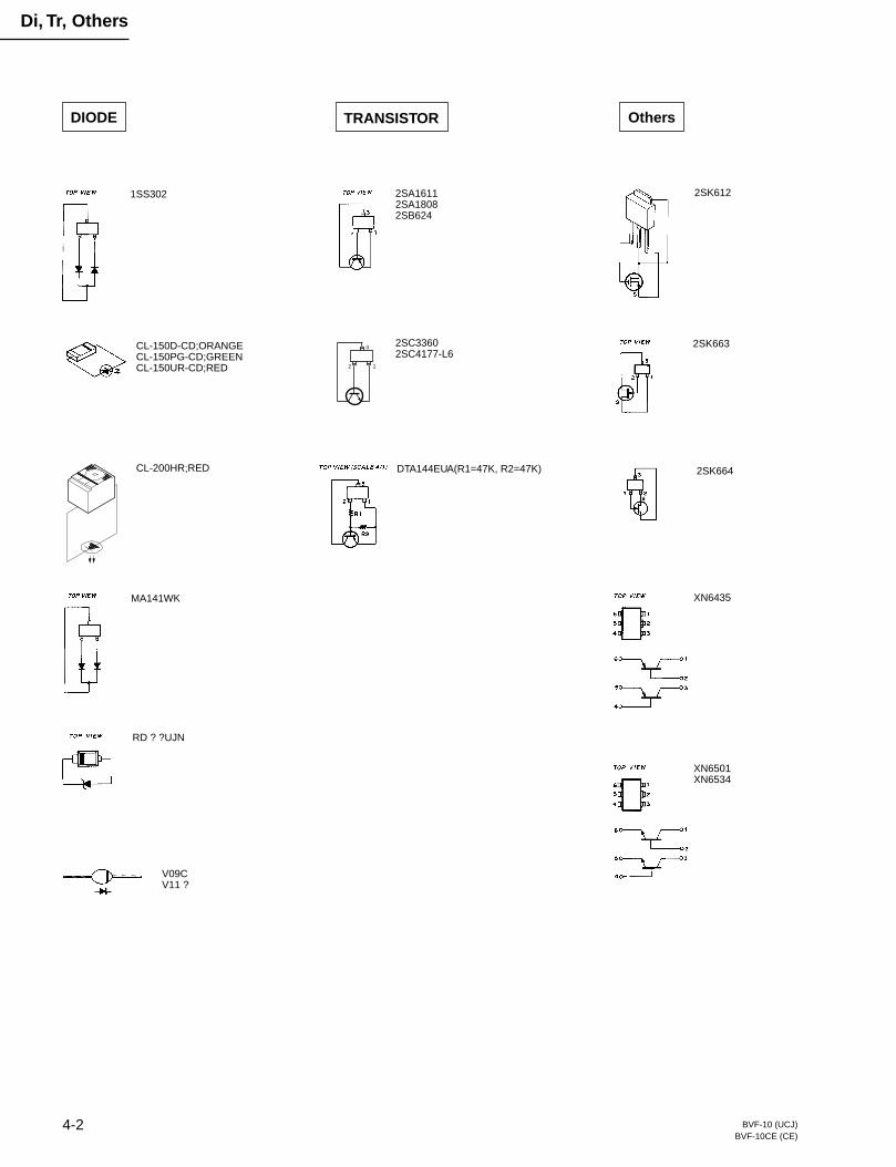
DIODE
1SS302
CL-150D-CD;ORANGECL-150PG-CD;GREENCL-150UR-CD;RED
MA141WK
RD ? ?UJN
V09CV11 ?
Others
2SK612
2SK663
TRANSISTOR
2SA16112SA18082SB624
2SC33602SC4177-L6
12
3
XN6435
XN6501XN6534
CL-200HR;RED( )
DTA144EUA(R1=47K, R2=47K) 2SK664
Di, Tr, Others
4-3BVF-10 (UCJ)BVF-10CE (CE)
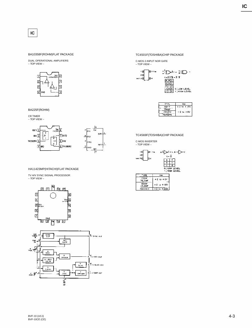
IC
TC4S01F(TOSHIBA)CHIP PACKAGE
C-MOS 2-INPUT NOR GATE– TOP VIEW –
TC4S69F(TOSHIBA)CHIP PACKAGE
C-MOS INVERTER– TOP VIEW –
BA225F(ROHM)
CR TIMER– TOP VIEW –
HA11423MP(HITACHI)FLAT PACKAGE
TV H/V SYNC SIGNAL PROCESSOR– TOP VIEW –
BA10358F(ROHM)FLAT PACKAGE
DUAL OPERATIONAL AMPLIFIERS– TOP VIEW –
IC

5-1BVF-10 (UCJ)
BVF-10CE (CE)5-1
TO CAMERA HEAD
20PIN CONNECTOR Q11
CLAMP
BATT
G TALLY
REC
D1
BATT
D3
G TALLY
D2
REC
D1
ABNORMAL
D3
VTR SAVE
D2
REC
21-1
21-3
21-2
LP-84
ABNORMAL
VTR SAVE
REC
31-1
31-3
31-2
LP-85
VR-199(1/3)
IC1
TIMER
7
5
1
3
Q3(1/2)
Q3(2/2)
Q1
DRIVER
Q2
DRIVER
Q4(1/2)
INV.
Q4(2/2)
INV.
D1,2
TALLY
REC CONT
REC
ZEBRA
MOMENTARY
TALLY OUT
11-4
11-5
11-6
11-7
11-12
1-12
1-4
1-3 1-14
2-1
2-3
2-2
1-7 1-8
2-6
2-8
2-7
1-6 1-18
3-11
3-10
3-9
1-17
3-8
3-3
1-15
1-9
VIDEO IN
AUDIO IND
G TALLY BATT IND
BATT
G TALLY
REC
VTR SAVE ABNORMAL
ABNORMAL
VTR SAVE
REC(L)
REC TALLY REC(L)
REC CONT
REC
ZEBRA
ZEBRA
MOMENTARY
TALLY OUT
CCIR/EIA
16:9
S1
AUDIO
ON OFF
Q1
DRIVER
Q2
DRIVER
SL1
SL2
SL3
SL4
SL5 SL6
H1
OFF
LOW
S2
ZEBRAON
OFF
MOMENTARY
S3
TALLY
D12
BACK TALLY
3-6VIDEO VIDEO
11-9
RV2 CONTRAST
11-8
VR-199(2/3)
3-7
Q3
BUFF
DL1 80ns
DELAY
Q4,5
BUFF
INV.
Q6
BUFF
Q7BLKG
CLEAN
RV9
SUB BRIGHT
3-5
3-2
PEAKING
+50V
11-10
11-13
3-4
3-1
RV3
PEAKING
11-11
11-14
RV1
BRIGHT
VR-199(3/3)
PEAKING
BRIGHT CTL
Q8,9
AMP
Q10
BUFF
TP2
Q12
RV3
H HOLD
+9.3V Q17
RIPPLE FILTER
IC1
12
11
13
8
AFC GATE
SYNC SEP.
C28,D7
CLAMP
Q18
5
+9.3V Q13,IC2
VOLTAGE REG.
RV1
H SIZE
IC1
14
7
6 4 2
1
18
16H OSC
H DRIVER
V BLKG
V DRIVERV OSC
RV5
V HOLD
RV4
V SIZE
(PAL ONLY)
IC3
2 4
T1
Q14 Q15 C12
C11
TP1
IC2
COMP7
5 6
RV8
HEATER
RV2
ANODE SET
1 2
44
Q19
AMP
Q20,21
V DRIVER
TP3
RV6
V SIZE
RV7
L IN
Q22
Q16
INV.
RV10
V SIZE(WIDE)
TP5
TP4
G1 OUT
5-5
H1 OUT
H2 OUT
5-4
5-3
G2 OUT 5-1
-H DEF
+H DEF
+V DEF
-V DEF
4-4
4-5
4-2
4-3
G2
H1
H2
G1
H.DY
CRTANODE
V.DY
VF-60
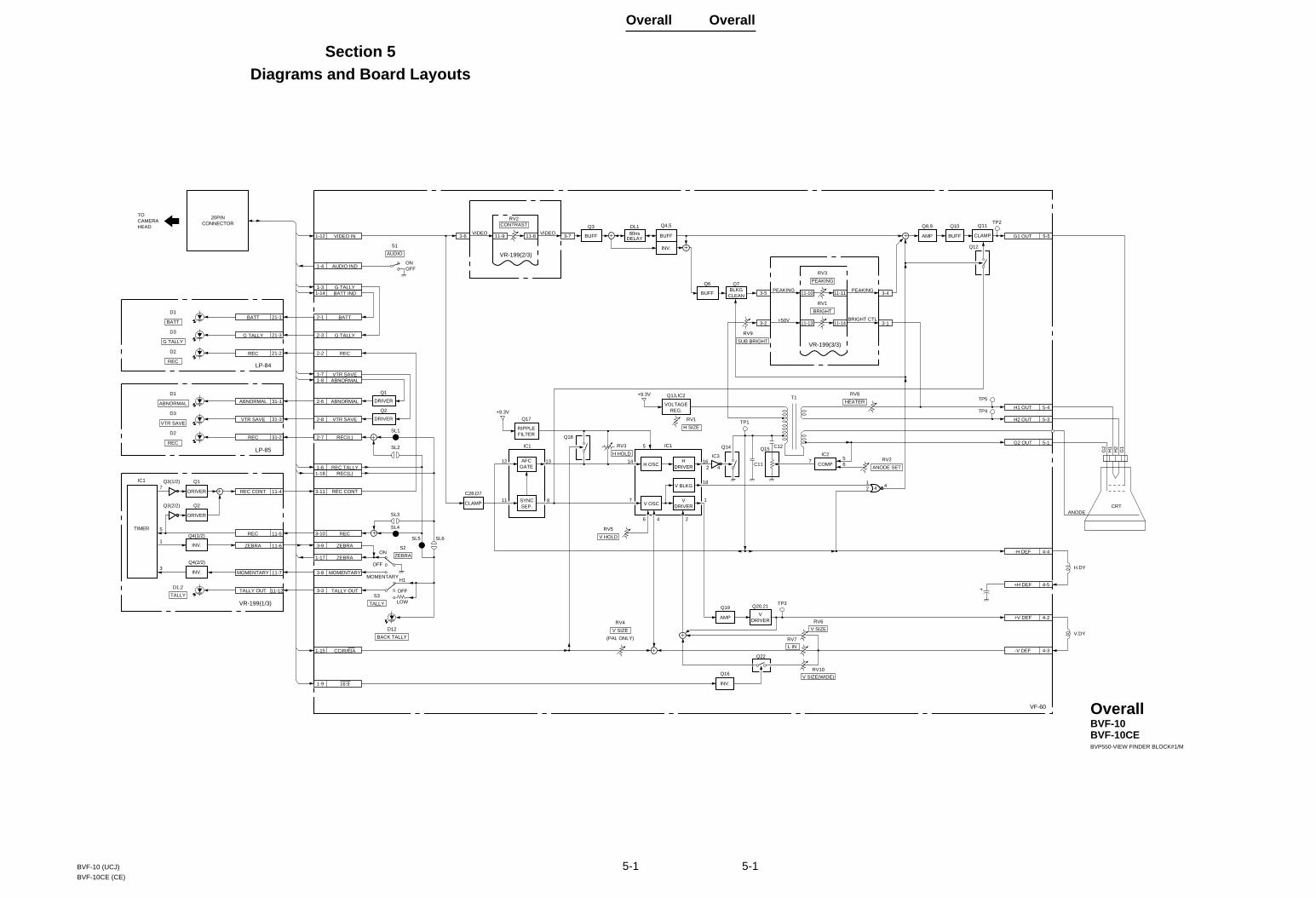
Section 5Diagrams and Board Layouts
Overall Overall
OverallBVF-10BVF-10CEBVP550-VIEW FINDER BLOCK#1/M
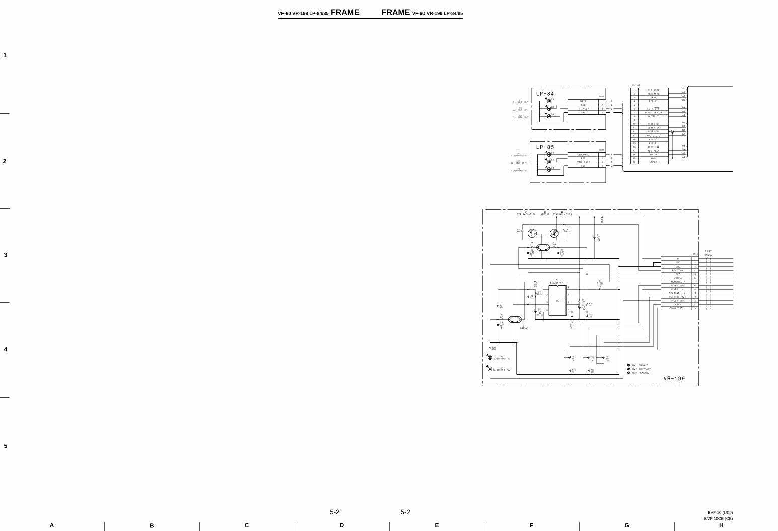
5-2 BVF-10 (UCJ)
BVF-10CE (CE)5-2
1
2
3
4
1
2
3
4
1
2
3
4
5
6
7
8
9
10
11
12
13
14
D3
CL-150PG-CD-T
D2
CL-150UR-CD-T
D1
CL-150UR-CD-T
CN21
CN31
D1
CL-150D-CD-T
D2
CL-150UR-CD-T
D3
CL-150D-CD-T
R2
560
R7
680k
R13
22k
CN11
C7
0.1
25V
F
Q2DTA144EUAT106
Q3XN6501
Q1DTA144EUAT106
Q4XN6501
C4
0.022
25V
B
R10
0
R12
NM
C6
15
16V
:TA-CC
C8
0.01
50V
B
R11
47k
R8
47k
R6
22k
C5
4.7
16V
R9
56k
R16
560
RV1
10k
(B)
RV2
1k
(B)
R15
47k
RV3
10k
(C)
C1
47
16V
:TA
R1
33
R5
22k
R4
22k
R3
8.2k
C2
0.01
50V
B
C3
0.01
50V
B
R14
470
D1
CL-200HR-C-TUL
D2
CL-200HR-C-TUL
IC1BA225F-T2
1
2
3
4 5
6
7
8
A7
A8
A9
B9
B6
B3
B4
B5
A6
A1
A2
A4
A3
B8
B7
0
1
2
3
0
6
7
8
1
2
3
4
5
6
7
8
9
10
11
12
13
14
15
16
17
18
19
20
VTR SAVE
ABNORMAL
REC(L)
CCIR/
G TALLY
AUDIO IND ON
ZEBRA ON
VIDEO(X)
AUDIO CTL
VIDEO(G)
MIC(Y)
MIC(X)
BATT IND
REC/ALLY
+9.3V
GND
UNREG
EIA
CN101
CABLE
FLAT
16-9
BATT
REC
G TALLY
GND
D1
D2
D3
LP-84
REC
GND
D1
D2
D3
ABNORMAL
VTR SAVE
LP-85
IC1
9V
GND
REC CONT
REC
ZEBRA
MOMENTARY
VIDEO IN
VIDEO OUT
PEAKING IN
PEAKING
+50V
BRIGHT CTL
TALLY OUT
OUT
RV1:BRIGHT
RV2:CONTRAST
RV3:PEAKING
GND
VR-199
2
1
3
4
5
A B C D E F G H
VF-60 VR-199 LP-84/85 FRAME FRAME VF-60 VR-199 LP-84/85
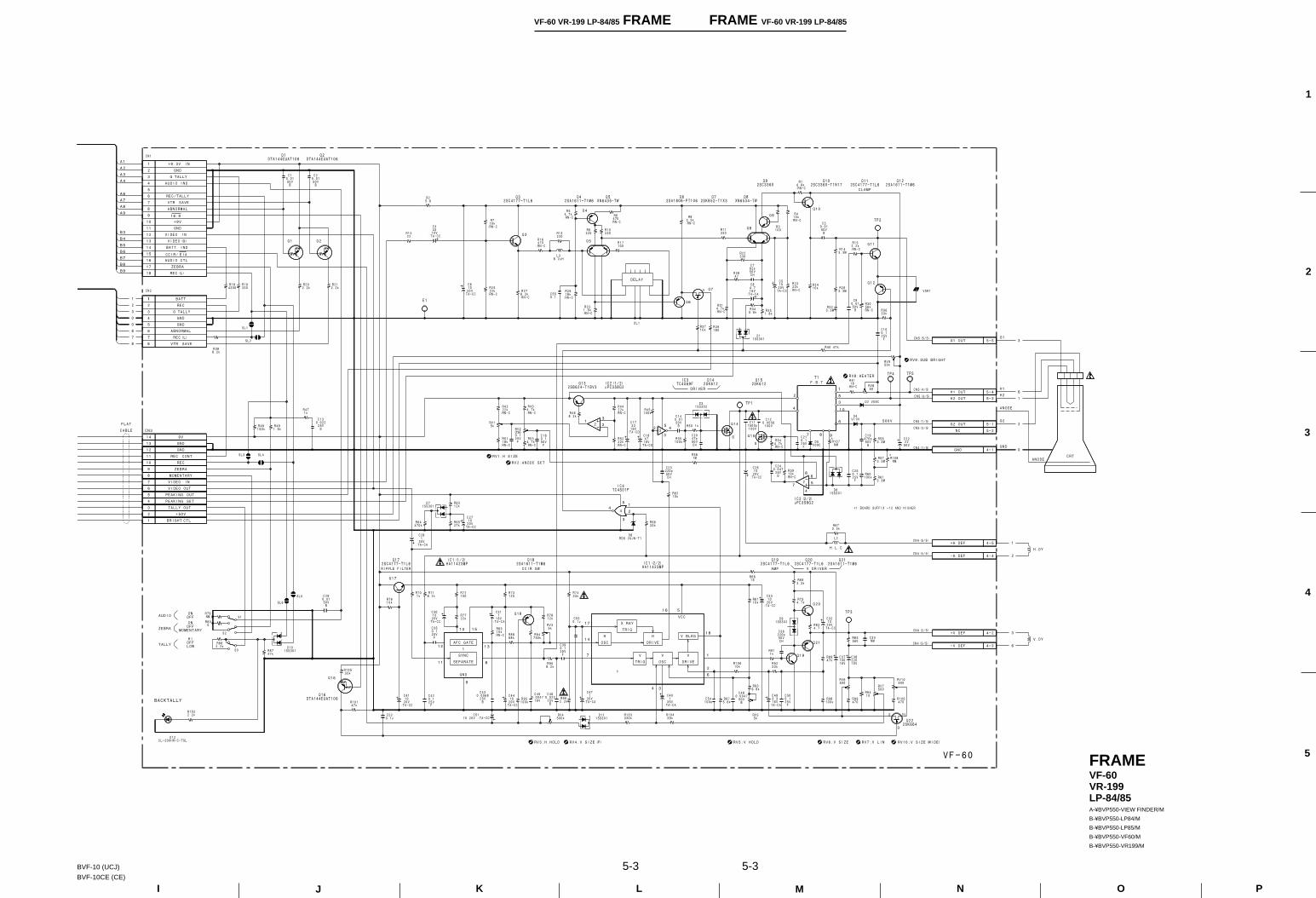
5-3BVF-10 (UCJ)
BVF-10CE (CE)5-3
FRAMEVF-60VR-199LP-84/85A-¥BVP550-VIEW FINDER/M
B-¥BVP550-LP84/M
B-¥BVP550-LP85/M
B-¥BVP550-VF60/M
B-¥BVP550-VR199/M
I J K L M N O P
5
4
3
2
1
VF-60 VR-199 LP-84/85 FRAME FRAME VF-60 VR-199 LP-84/85
V
DRIVE
V
OSC
V
TRIG
H
DRIVE
X RAY
TRIG
H
OSC
VCC
V BLKG
AFC GATE
SYNC
SEPARATE
GND
S
S
DELAY
1
2
3
4
5
6
7
8
9
10
11
12
13
14
15
16
17
18
S1
S2
S3
L2
T1
L3
8.2µH
VDR1
SL3
CN1
SL4
Q202SC4177-T1L6
RV1
5k
RV2
1k
RV9
50k
RV10
500
RV7
500
RV6
500
RV5
5k
RV4
500k
RV3
5k
R3
100
R4
10k
:RN-C
R5
4.7k
:RN-CR6
470
:RN-CR7
10k
:RN-C
R9
220
R10
220R13
220
R15
2.2k
:RN-C
R16
470
:RN-C
R17
100
R19
330
R22
330
R23
22k
:RN-C
R24
10kR25
22k
:RN-C
R27
8.2k
:RN-C
R28
47
R29
18k
:RN-C
R30
56k
:RN-C
R31
4.7k
:RN-C
R32
3.3MR34
5.6kR35
1.8k
R37
10kR39
180
R41
18
:RN-C
R42
22k
:RN-C
R44
22k
:RN-C
R45
100kR46
8.2k
R47
1k
R50 1k
R51
18k
:RN-C
R52
22k
:RN-C
R53
4.7k
:RN-C
R55
100k
R58
1M
R62
10k
R63
12k
R64
470k
R65
27k
R66
33k R67
3.3k
R68
15 R69
3.3k
R70
1k
R71
8.2k
R72
100
R73
120
R74
33k
R75
4.7k
R76
10k
R77
22k
R78
12k
R81
10k
R82
4.7
R84
750k R85
560R86
2.2k
R87
47k
R88
68k
R89
47k
R90
8.2k
R91
1k
R92
33k
R93
6.8k
R94
10
R95
100k
R96
2.2kR97
5.6k
R98
100k
R99
470
R100
470
R102
2.2k R103
330k
R104
39k
C5
10
20V
:TA-CC
C6
10
20V
:TA-CC
C27
10
20V
:TA-CC
C30
10
20V
:TA-CC
C31
1
16V
:TA-CA
C32
10
20V
:TA-CC
C33
10
20V
:TA-CC
C37
100
16V
C41
10
20V
:TA-CC
C44
10
20V
:TA-CC
C51
10 20V :TA-CC
D1
1SS301
D4
V11N
D5
V09C
D6
1SS301
D12
CL-200HR-C-TSL
C38
220
10V
R43
4.7k
:RN-C
C3
0.01
50V
B
C9
0.01
50V
B
C13
0.022
25V
B
C15
0.1
25V
F
C20
47p
50V
CH
C29
0.01
50V
B
C35
0.1
25V
F
C48
0.0047
50V
B
C50
0.1
25V
F
R33
1.5k
:RN-C
C43
0.0068
25V
B
C53
0.1µ
C54
100p
R106
10k
C34
NM
R8
3.3k
:RN-C
R11
330
C17
33
16V
:TA-CD
C55
0.1
R59
10k
:RN-C
R83
10k
:RN-C
C4
33
10V
:TA-CC
C49
3.3
16V
:TA-CA
C40
1
35V
:TA-CA
C47
1
35V
:TA-CA
CN2
Q2DTA144EUAT106
Q1DTA144EUAT106
C2
0.01
50V
B
C1
0.01
50V
B
R12
22
R38
8.2k
SL2
SL1
R2
5.6
E1
Q32SC4177-T1L6
Q42SA1611-T1M6
C7
82p
50V
CH
C8
4.7
16V
:TA-CA
Q112SC4177-T1L6
Q122SA1611-T1M6
R1
6.8k
:RN-C
Q102SC3360-T1N17
R36
33k
C10
0.1
25V
F
R26
3.3M
R14
3.3M
C16
0.1
50V
F
C18
47
16V
:TA-CD
Q132SB624-T1BV3
IC2(1/2)µPC358G2
C14
0.01
50V
B
D3
1SS302
C23
220p
50V
CH
C11
1500p
100V
C12
0.0056
100V
R54
4.7k
:RN-C
C24
0.047
25V
B
C26
10
20V
:TA-CC
C21
0.1
25V
F
R40 47k
C22
22
50V
R56
3.3M
C19
470p
50V
B
R57
3.3MR108
NM
R61
3.3M
R60
100k
R107
NM
C25
0.1
25V
F
RV8
50
D2 V09C
TP5
Q152SK612
C28
1
35V
:TA-CA
D7
1SS301
Q172SC4177-T1L6
IC1(1/2)HA11423MP
Q182SA1611-T1M6
C36
220p
50V
CH
D9
1SS302
TP3
Q192SC4177-T1L6
Q222SK664
Q72SK852-T1X3
Q62SA1808-PT106
Q8XN6534-TW
Q92SC3360
TP2
R80
0
C52
0.1µ
D11
1SS301
R49
1.5k
R48
150k
R21
2.2k
R20
2.2k
R18
4300
Q16DTA144EUAT106
IC3TC4S69F
Q142SK612
IC2(2/2)µPC358G2
IC4TC4S01F
TP4
TP1
D10
1SS301
R101
47k
R105
33k
C42
0.1
25V
F
C46
0.022
25V
B
C45
0.0047
16V
C39
0.1
25V
F
Q212SA1611-T1M6IC1(2/2)
HA11423MP
D8
RD6.2UJN-T1
SL5
SL6
DL1
Q5XN6435-TW
CN5(1/5)
CN5(2/5)
CN5(3/5)
CN5(4/5)
CN5(5/5)
CN4(1/5)
CN4(2/5)
CN4(3/5)
CN4(4/5)
CN4(5/5)
R79
NM
1
2
3
7
4
5
68
2
3
4
1
2
3
4
12
11
9
8
13
1510
17
14
7
4 3
6
2
1
18
516
5
5
1
2
3
4
5
6
7 8
10
9
2
3
1
A1
A2
A3
A4
A6
A7
A8
A9
B3
B4
B5
B6
B7
B8
B9
1
2
3
0
0
6
7
8
CABLE
FLAT
H.DY
V.DY
1
2
3
6
G1
H1
H2
ANODE
G2
GND
3
6
1
2
0
ANODECRT
+9.3V
+9V
GND
GND
G TALLY
IN
VIDEO IN
AUDIO IND
VIDEO(G)
BATT IND
REC/TALLY
EIACCIR/
VTR SAVE
AUDIO CTL
ABNORMAL
ZEBRA
REC(L)
AUDIO
ON
OFFZEBRA
MOMENTARY
TALLYLOW
OFF
HI
OFF
ON
V DRIVERAMPCCIR SW
RV3;H.HOLD RV5;V HOLD RV6;V SIZE RV7;V LIN
H.L.C
RIPPLE FILTER
F.B.T
S
S
RV1;H SIZE
RV2;ANODE SET
G1 OUT
H1 OUT
H2 OUT
G2 OUT
GND
+H DEF
-H DEF
+V DEF
-V DEF
CLAMP
DRIVER
500V
NC 5-2
5-5
5-4
5-3
5-1
4-1
4-5
4-4
4-2
4-3
2
2
3
4
RV9;SUB BRIGHT
RV4;V SIZE(P)
RV8;HEATER
RV10;V SIZE(WIDE)
16:9
1
2
1
3
4
5
6
7
8
REC
BATT
G TALLY
GND
GND
ABNORMAL
VTR SAVE
REC(L)
9V
GND
REC CONT
REC
ZEBRA
MOMENTARY
VIDEO IN
VIDEO
PEAKING
PEAKING
+50V
BRIGHT CTL
TALLY OUT
SET
BACKTALLY
Q20
Q21
Q19
Q18
Q17
Q16
Q14
Q15
Q12
Q11
Q8
Q9
Q7
Q6
Q5
Q4
Q3
Q2Q1
OUT
OUT
CN3
1
3
2
4
5
6
7
8
9
10
11
12
13
14
GND
VF-60
Q10
1
1
*
*
*1:BOARD SUFFIX -12 AND HIGHER
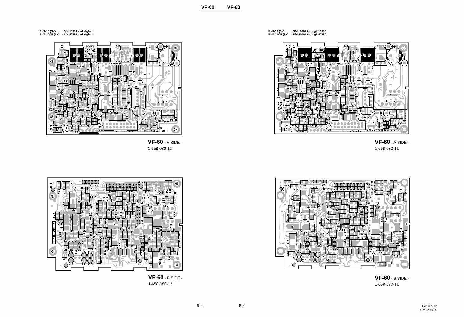
5-4 BVF-10 (UCJ)
BVF-10CE (CE)5-4
VF-60 VF-60
VF-60 - B SIDE -
1-658-080-11
VF-60 - A SIDE -
1-658-080-11
VF-60 - A SIDE -
1-658-080-12
VF-60 - B SIDE -
1-658-080-12
BVF-10 (SY) : S/N 10851 and HigherBVF-10CE (SY) : S/N 40781 and Higher
BVF-10 (SY) : S/N 10001 through 10850BVF-10CE (SY) : S/N 40001 through 40780
The material contained in this manual consists ofinformation that is the property of Sony Corporation andis intended solely for use by the purchasers of theequipment described in this manual.Sony Corporation expressly prohibits the duplication ofany portion of this manual or the use thereof for anypurpose other than the operation or maintenance of theequipment described in this manual without the expresswritten permission of Sony Corporation.
Le matériel contenu dans ce manuel consiste eninformations qui sont la propriété de Sony Corporation etsont destinées exclusivement à l’usage des acquéreursde l’équipement décrit dans ce manuel.Sony Corporation interdit formellement la copie dequelque partie que ce soit de ce manuel ou son emploipour tout autre but que des opérations ou entretiens del’équipement à moins d’une permission écrite de SonyCorporation.
Das in dieser Anleitung enthaltene Material besteht ausInformationen, die Eigentum der Sony Corporation sind,und ausschließlich zum Gebrauch durch den Käufer derin dieser Anleitung beschriebenen Ausrüstung bestimmtsind.Die Sony Corporation untersagt ausdrücklich dieVervielfältigung jeglicher Teile dieser Anleitung oder denGebrauch derselben für irgendeinen anderen Zweck alsdie Bedienung oder Wartung der in dieser Anleitungbeschriebenen Ausrüstung ohne ausdrücklicheschriftliche Erlaubnis der Sony Corporation.

Printed in Japan
Sony Corporation 1997. 5 08
Broadcast Products Company ©1995
Published by Broadcast Products Company
BVF-10 (UCJ)
BVF-10CE (CE) J, E
3-190-295-03


