18
SOT-MRAM RESEARCH OVERVIEW, CHALLENGES AND CURRENT MARKET TRENDS Authors: Dr. Gaurav Santhalia & Riya Dahiya
SOT-MRAM RESEARCH OVERVIEW, CHALLENGES
AND CURRENT MARKET TRENDS
Authors: Dr. Gaurav Santhalia & Riya Dahiya
INTRODUCTION
With the beginning of mobile and handheld electronic devices, the demand for much smaller, faster and
ultra-low power systems keeps growing. To meet such needs, the microelectronics industry can no
longer rely on Moore’s law.
MRAM is becoming more attractive in industry because of its promising prospects for replacing or
extending existing random-access memories and being a promising candidate to the universal non-
volatile (NV) storage device.
SOT-MRAM was first proposed in 2013, and since then research is going on to make it in practical use.
The presence of separate read and write paths in SOT-MRAM, overcomes the shortcomings of STT-
MRAM. It is supposed that by the fall of 2021 SOT-MRAM might be commercially available.
WHAT IS MRAM?
Unlike conventional RAMs that store data as electrical charges, MRAM (Magnetoresistive Random Access
Memory) is a non-volatile memory in which data bits are stored using the magnetization (electrons spin)
orientation.
MRAM offers a number of advantages compared to existing semiconductor technologies, as it is
intrinsically nonvolatile, requires low operating power and has good endurance.
The first generation of MRAM was based upon the so-called toggle technology, used electrical currents
to induce the magnetic field in the MTJ to read or write the cell, but that requires more power than is
ideal for modern computer systems. Succeeding generations started to use another method called Spin
Torque Transfer (STT) MRAM. STT-MRAM uses a spin-polarized current to write data resulting in lower
and scalable switching currents , hence in higher density memory products.
MAGNETIC TUNNEL JUNCTION (MTJ)
MTJ is the heart of MRAM. A MTJ is composed of two ferromagnetic layers separated by a thin insulating
layer. One of the plates is a permanent magnet set to a particular polarity (fixed layer). While the
magnetization of the other plate can be changed to match that of an external field to store memory (free
layer). Reading is accomplished by measuring the electrical resistance of the cell. Because of tunnel
magnetoresistance, the electrical resistance of the cell changes with the relative orientation of the
magnetization in the two plates.
Typically if the two plates have the same magnetization alignment (low resistance state) this is
considered to mean "1", while if the alignment is antiparallel the resistance will be higher (high resistance
state) and this means "0".Writing consists of switching the magnetization of the free layer from one
direction to the other, which can be done by a magnetic field, STT or SOT
SOT – MRAM
Spin Orbit Torque Magnetic Random-Access Memory (SOT-MRAM) is the latest generation of MRAM.
SOT is gaining interest as it comes with all the benefits of its predecessor STT-MRAM, but also eliminates
some of its shortcomings. It is an alternative spin current source originating from the spin-orbit interaction
and mediated by Spin Hall and Rashba effects
The storage device in SOT memories is a MTJ cell where the data is stored as a resistance state value (0
or 1). The SOT-MRAM uses a three terminal MTJ-based concept to isolate the read and the write path
unlike a 2-terminal concept in STT. The terminals comprise a read line, a write line, a source line and a
word line.
The word line is used to access the required bit-cell during memory accesses. If the access is a read
operation, the source line is connected to the ground while the read line is used to measure the MTJ
resistance by sensing the current flow in MTJ. During the write operation the current flows between the
source line and the write line. MTJ resistance will be low if current flows from source to write line and
high if it flows from write to source line.
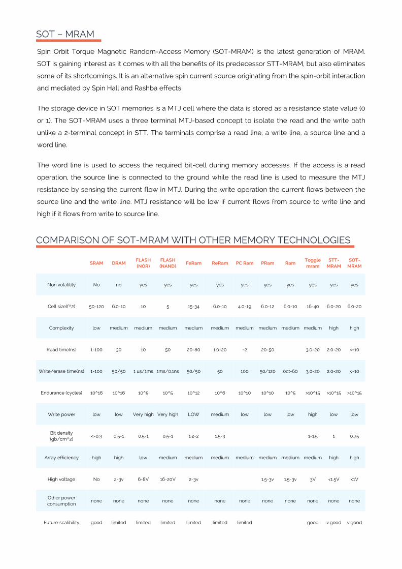
COMPARISON OF SOT-MRAM WITH OTHER MEMORY TECHNOLOGIES
SRAM DRAMFLASH(NOR)
FLASH(NAND)
FeRam ReRam PC Ram PRam RamToggle mram
STT-MRAM
SOT-MRAM
Non volatility No no yes yes yes yes yes yes yes yes yes yes
Cell size(f^2) 50-120 6.0-10 10 5 15-34 6.0-10 4.0-19 6.0-12 6.0-10 16-40 6.0-20 6.0-20
Complexity low medium medium medium medium medium medium medium medium medium high high
Read time(ns) 1-100 30 10 50 20-80 1.0-20 ~2 20-50 3.0-20 2.0-20 <=10
Write/erase time(ns) 1-100 50/50 1 us/1ms 1ms/0.1ns 50/50 50 100 50/120 0ct-60 3.0-20 2.0-20 <=10
Endurance (cycles) 10^16 10^16 10^5 10^5 10^12 10^6 10^10 10^10 10^5 >10^15 >10^15 >10^15
Write power low low Very high Very high LOW medium low low low high low low
Bit density(gb/cm^2)
<=0.3 0.5-1 0.5-1 0.5-1 1.2-2 1.5-3 1-1.5 1 0.75
Array efficiency high high low medium medium medium medium medium medium medium high high
High voltage No 2-3v 6-8V 16-20V 2-3v 1.5-3v 1.5-3v 3V <1.5V <1V
Other power consumption
none none none none none none none none none none none none
Future scalibility good limited limited limited limited limited limited good v.good v.good
NEED OF SOT – MRAM
» SOT MRAM was basically designed to meet the demands of devices that require an energy-efficient
network of smart nodes that need to be always powered on, always connected, and always aware,
with low active duty cycles
» SOT can be easily implemented on STT-MRAM manufacturing lines, therein supporting a quick market
deployment in applications as diverse as Internet of Things (IoT), mobile, computing and storage. SOT
memories are excellent for on-chip memory, not only for the last-level cache, but also for lower levels
of cache.
» SOT-MRAM offers a much higher density, unlimited scalability, lower energy consumption, is radiation
immune and non-volatile making it a viable candidate to replace existing memories in in virtually all
semiconductor chips, from microcontrollers to microprocessors and systems-on-chip. It will be some
time before SOT-MRAM reaches the finish line, but the prospects definitely make the journey worth
the effort.
KEY PROBLEMS FACED BY SOT TO BECOME WIDELY AVAILABLE
The practical, physical implementation of scalable, commercially accessible quantum computers
still has several practical obstacles.
» SOT-MRAM is less vulnerable to radiation, but suffers from retention failures due to an inherent
thermal instability. This thermal instability can lead to data loss, hence negatively affecting the
retention time of SOT-MRAM
» For small cache sizes it takes longer read and write access latencies compared to SRAM.
» The main roadblock towards the integration of the SOT-MRAM is that the reproducible bipolar
switching requires the application of a static in-plane magnetic field. “Zero-field” SOT switching is still
a challenge that motivates active research on this topic.
» A pure SOT-MRAM based configuration is on average the most energy efficient solution, but it is also
the most area demanding approach
» Lowering the energy demand and enhancing the energy efficiency is an outstanding problem for the
SOT-MRAM.
» Today, though, the biggest problem with SOT-MRAM is that it only switches about 50% of the time.
» For small memory capacities, the scaling of SOT-MRAM is limited by the size of the memory periphery,
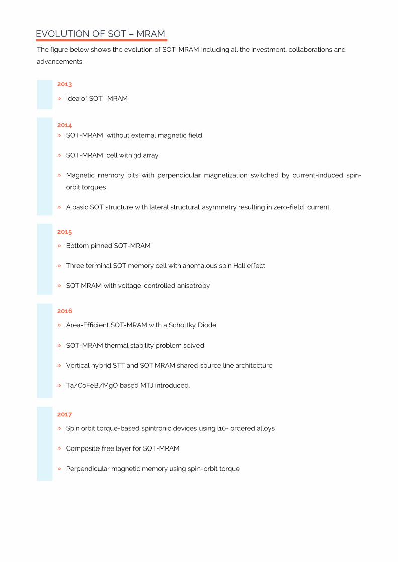
EVOLUTION OF SOT – MRAM
The figure below shows the evolution of SOT-MRAM including all the investment, collaborations and
advancements:-
» Idea of SOT -MRAM
2013
» SOT-MRAM without external magnetic field
» SOT-MRAM cell with 3d array
» Magnetic memory bits with perpendicular magnetization switched by current-induced spin-
orbit torques
» A basic SOT structure with lateral structural asymmetry resulting in zero-field current.
2014
» Bottom pinned SOT-MRAM
» Three terminal SOT memory cell with anomalous spin Hall effect
» SOT MRAM with voltage-controlled anisotropy
2015
» Area-Efficient SOT-MRAM with a Schottky Diode
» SOT-MRAM thermal stability problem solved.
» Vertical hybrid STT and SOT MRAM shared source line architecture
» Ta/CoFeB/MgO based MTJ introduced.
2016
» Spin orbit torque-based spintronic devices using l10- ordered alloys
» Composite free layer for SOT-MRAM
» Perpendicular magnetic memory using spin-orbit torque
2017
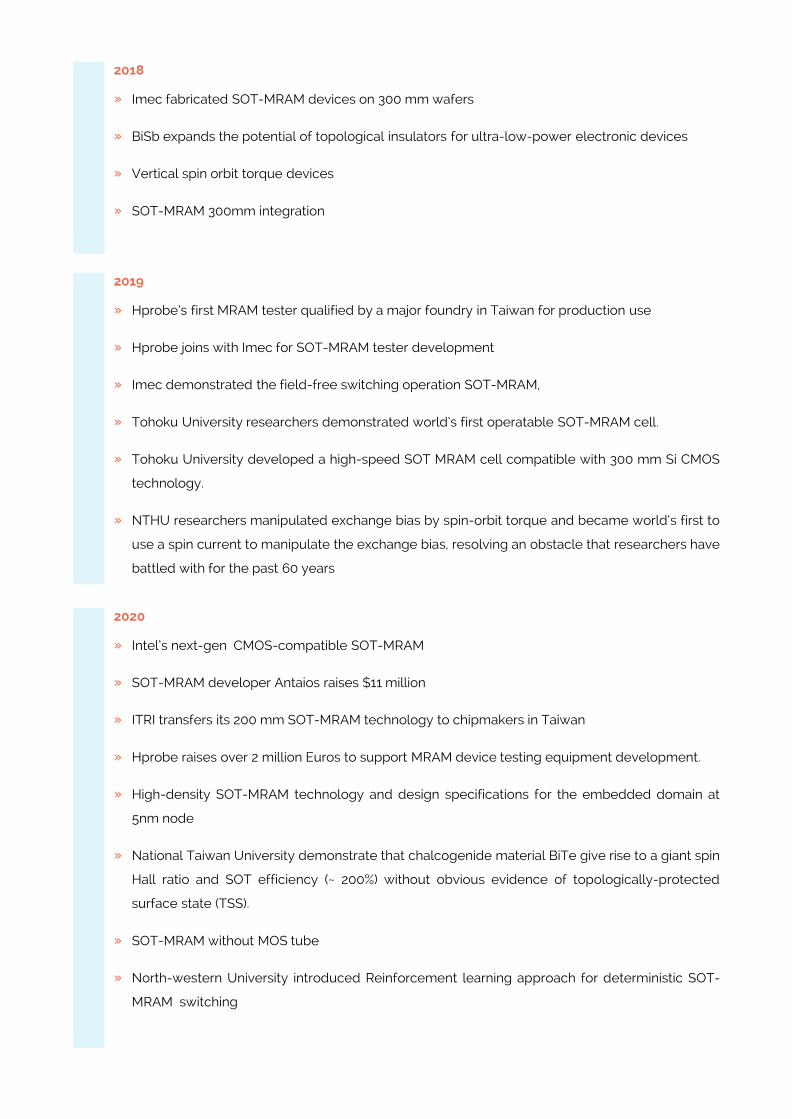
» Imec fabricated SOT-MRAM devices on 300 mm wafers
» BiSb expands the potential of topological insulators for ultra-low-power electronic devices
» Vertical spin orbit torque devices
» SOT-MRAM 300mm integration
2018
» Hprobe’s first MRAM tester qualified by a major foundry in Taiwan for production use
» Hprobe joins with Imec for SOT-MRAM tester development
» Imec demonstrated the field-free switching operation SOT-MRAM,
» Tohoku University researchers demonstrated world’s first operatable SOT-MRAM cell.
» Tohoku University developed a high-speed SOT MRAM cell compatible with 300 mm Si CMOS
technology.
» NTHU researchers manipulated exchange bias by spin-orbit torque and became world’s first to
use a spin current to manipulate the exchange bias, resolving an obstacle that researchers have
battled with for the past 60 years
2019
» Intel’s next-gen CMOS-compatible SOT-MRAM
» SOT-MRAM developer Antaios raises $11 million
» ITRI transfers its 200 mm SOT-MRAM technology to chipmakers in Taiwan
» Hprobe raises over 2 million Euros to support MRAM device testing equipment development.
» High-density SOT-MRAM technology and design specifications for the embedded domain at
5nm node
» National Taiwan University demonstrate that chalcogenide material BiTe give rise to a giant spin
Hall ratio and SOT efficiency (~ 200%) without obvious evidence of topologically-protected
surface state (TSS).
» SOT-MRAM without MOS tube
» North-western University introduced Reinforcement learning approach for deterministic SOT-
MRAM switching
2020
» ISI ships its first SOT-MRAM tester system
» Hprobe announces a significant order for MRAM testing equipment from a tier-1 semiconductor
manufacturer
» Korea University develops high-efficiency magnetic memory core material using tungsten-
vanadium alloy.
» IIT Delhi in collaboration with National University of Singapore develops device to reduce
frequency of charging electronic goods
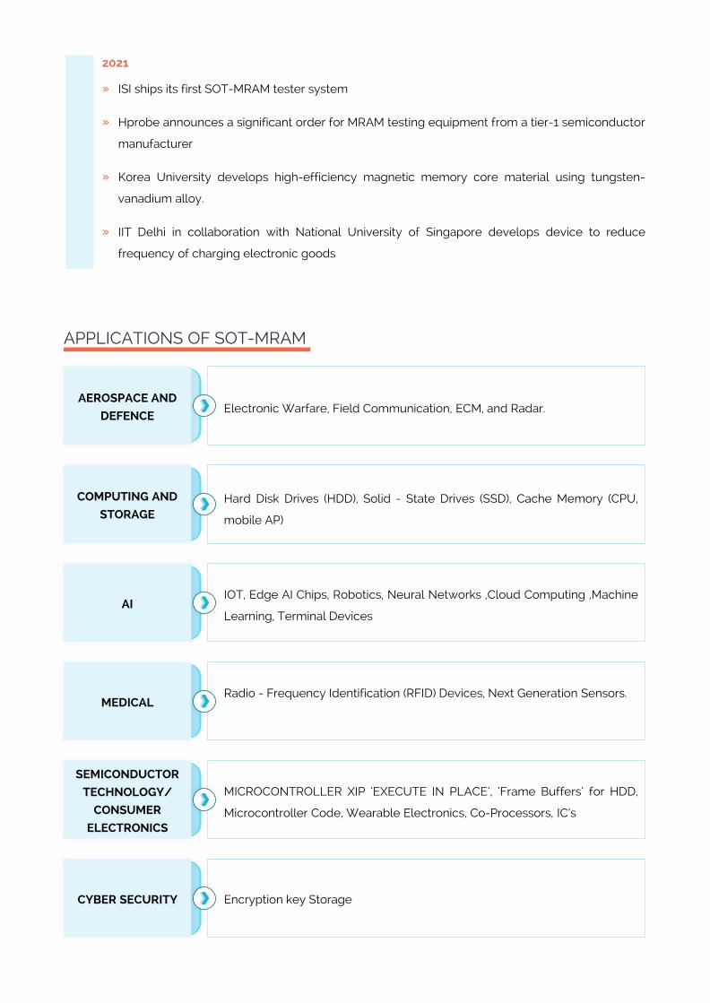
2021
APPLICATIONS OF SOT-MRAM
AEROSPACE AND
DEFENCEElectronic Warfare, Field Communication, ECM, and Radar.
COMPUTING AND
STORAGEHard Disk Drives (HDD), Solid - State Drives (SSD), Cache Memory (CPU,
mobile AP)
AIIOT, Edge AI Chips, Robotics, Neural Networks ,Cloud Computing ,Machine
Learning, Terminal Devices
MEDICALRadio - Frequency Identification (RFID) Devices, Next Generation Sensors.
SEMICONDUCTOR
TECHNOLOGY/
CONSUMER
ELECTRONICS
MICROCONTROLLER XIP ‘EXECUTE IN PLACE’, ‘Frame Buffers’ for HDD,
Microcontroller Code, Wearable Electronics, Co-Processors, IC’s
CYBER SECURITY Encryption key Storage
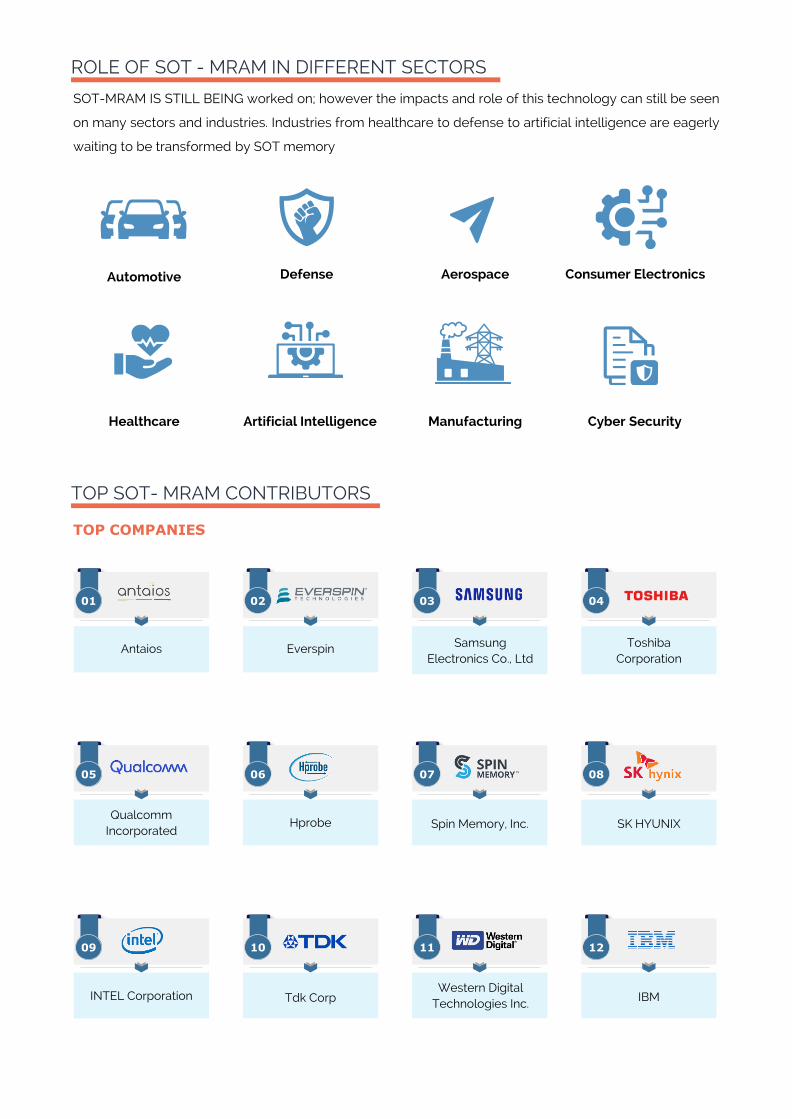
ROLE OF SOT - MRAM IN DIFFERENT SECTORS
SOT-MRAM IS STILL BEING worked on; however the impacts and role of this technology can still be seen
on many sectors and industries. Industries from healthcare to defense to artificial intelligence are eagerly
waiting to be transformed by SOT memory
Automotive Defense Aerospace Consumer Electronics
Healthcare Artificial Intelligence Manufacturing Cyber Security
TOP SOT- MRAM CONTRIBUTORS
TOP COMPANIES
01
Antaios
02
Everspin
03
Samsung Electronics Co., Ltd
04
Toshiba Corporation
05
Qualcomm Incorporated
06
Hprobe
07
Spin Memory, Inc.
08
SK HYUNIX
09
INTEL Corporation
10
Tdk Corp
11
Western Digital Technologies Inc.
12
IBM
TOP UNIVERSITIES
RECENT INNOVATION IN DOMAIN
Adaptive Non-Uniform Compressive Sensing using SOT-MRAM Multi-bit Precision Crossbar
Arrays
» A Compressive Sensing (CS) approach is applied to utilize intrinsic computation capabilities of SOT-
MRAM devices for IOT applications wherein lifetime energy, device area, and manufacturing costs are
highly-constrained while the sensing environment varies rapidly.
» Using Adaptive Compressed-sampling via Multi-bit Crossbar Array (ACMCA) approach to intelligently
generate the CS measurement matrix using a multi-bit SOT-MRAM crossbar array.
» SPICE circuit and MATLAB algorithm simulation results indicate that ACMCA reduces reconstruction
error by up to 4dB using a 4-bit quantized CS measurement matrix while incurring a negligible increase
in the energy consumption of generating the matrix
National Tsing HuaUniversity
Tohoku University IIT Delhi Northwestern University Seoul's National University
Pohang's University of Science and
Technology (POSTECH)
Taiwan's Industrial Technology Research
Institute (ITRI)
National Taiwan University
Tohoku Institute of Technology
Tohoku Institute of Technology
CoTb SOT-MRAM device
» Device structure that enables deterministic switching without any need for bias magnetic fields.
» The new approach can be scaled to large wafers with good uniformity, since it doesn't rely on having a
structural asymmetry in the device. SOT-MRAM devices based on this structure could be faster and
more energy-efficient than current designs.
» The new SOT-MRAM device uses a material which is based on a multi-layered stack of ultrathin films
of CoTb. In addition material does not require any external magnetic fields, making it one of the most
efficient SOT materials reported to date
High-efficiency magnetic memory core material
» Professor Young-geun Kim's research team at Korea University develops high spin flow conversion
efficiency can be achieved by inducing alloying with vanadium (V). The tungsten-vanadium alloy
showed an improvement of about 40% or more in spin flow conversion efficiency compared to the
existing tungsten single thin film.
Chalcogenide materials found to be highly suitable for SOT-MRAM
» Researchers from National Taiwan University demonstrate that chalcogenide material BiTe with non-
epitaxial structure can give rise to a giant spin Hall ratio and SOT efficiency (~ 200%) without obvious
evidence of topologically-protected surface state (TSS).
» The researchers explain that a clear thickness-dependent increase of the SOT efficiency indicates that
the origin of this effect is from the bulk spin-orbit interaction of such materials system. Efficient
current-induced switching through SOT is also demonstrated with a low zero-thermal critical
switching current density (~ 6×10⁵ A/cm2).
CMOS compatible SOT-MRAM device
» Intel demonstrated a CMOS-compatible process of an SOT-MRAM device with a bilayer SOT bottom
electrode. the two-pulse field-free SOT switching scheme with spin-transfer torque assist at 10ns is
experimentally validated
» To develop the technology, new SOT bottom electrode (BE) structure was developed consisting of
two heavy-metal layers and an MTJ etch process that has a high selectivity between them. This allows
us to precisely control the over-etch thickness into the SOT BE across a 300 mm wafer
Device for High Density Magnetic Memory
» IIT Delhi Researcher in Collaboration with NUS demonstrated a shared write channel based multi-bit
SOT cell scheme, which reduces the number of transistors required per bit. This cell design requires
half the area compared to conventional SOT MRAM, thus almost doubles the area efficiency of the
memory chip”.
» To make the design feasible, the team designed a magnetic memory device, which can be
programmed by application of gate voltage. The gate voltage was used to migrate oxygen ions in the
device, which resulted in modulation of the spin current polarity. Thus, cells can now be written
individually, and hence they obtained a full-fledged, working area-efficient SOT memory
IP IMPLICATIONS
» In the era where technology is constantly evolving, innovation is crucial to the development and
deployment of technologies.
» Patents can play a prominent role in the entire technology life cycle, and allow competitive
technologies to be protected and licensed to third parties to expand financial opportunities, benefiting
the society as a whole. Not only does publishing of a patent improves the chances of better
technology becoming available in the future but also spark new ideas thus promoting new inventions
» Patenting can help stop unscrupulous third parties from free riding on the efforts of the
company/individual. If someone tries to submit a patent application of yours, patent systems always
promote the first to file and may generate complications. These concerns can be avoided by the
applicant while filing the patent application. However, SOT memories provide several issues for patent
attorneys notwithstanding the benefits of patent applications.
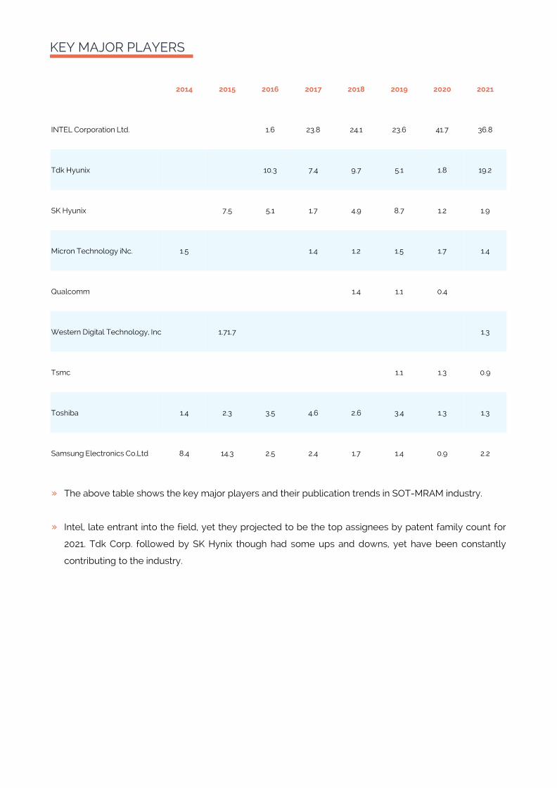
KEY MAJOR PLAYERS
2014 2015 2016 2017 2018 2019 2020 2021
INTEL Corporation Ltd. 1.6 23.8 24.1 23.6 41.7 36.8
Tdk Hyunix 10.3 7.4 9.7 5.1 1.8 19.2
SK Hyunix 7.5 5.1 1.7 4.9 8.7 1.2 1.9
Micron Technology iNc. 1.5 1.4 1.2 1.5 1.7 1.4
Qualcomm 1.4 1.1 0.4
Western Digital Technology, Inc 1.71.7 1.3
Tsmc 1.1 1.3 0.9
Toshiba 1.4 2.3 3.5 4.6 2.6 3.4 1.3 1.3
Samsung Electronics Co.Ltd 8.4 14.3 2.5 2.4 1.7 1.4 0.9 2.2
» The above table shows the key major players and their publication trends in SOT-MRAM industry.
» Intel, late entrant into the field, yet they projected to be the top assignees by patent family count for
2021. Tdk Corp. followed by SK Hynix though had some ups and downs, yet have been constantly
contributing to the industry.
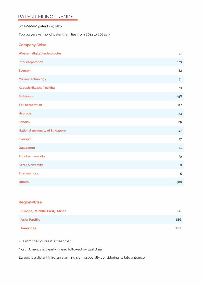
PATENT FILING TRENDS
SOT-MRAM patent growth:-
Top players vs. no. of patent families from 2013 to 2021p :-
Company-Wise
Western digital technologies 47
Intel corporation 123
Everspin 82
Micron technology 71
Kabushikikaisha Toshiba 79
SK hyunix 156
Tdk corporation 117
Hyprobe 53
Sandisk 29
National university of Singapore 27
Everspin 17
Qualcomm 11
Tohuku university 29
Korea University 9
Spin memory 5
Others 580
Region-Wise
Europe, Middle East, Africa 56
Asia Pacific 159
Americas 257
» From the figures it is clear that :
North America is clearly in lead followed by East Asia.
Europe is a distant third, an alarming sign, especially considering its late entrance.
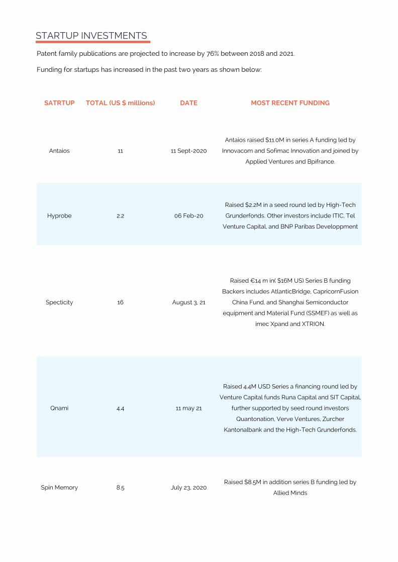
STARTUP INVESTMENTS
Patent family publications are projected to increase by 76% between 2018 and 2021.
Funding for startups has increased in the past two years as shown below:
SATRTUP TOTAL (US $ millions) DATE MOST RECENT FUNDING
Antaios 11 11 Sept-2020
Antaios raised $11.0M in series A funding led by
Innovacom and Sofimac Innovation and joined by
Applied Ventures and Bpifrance.
Hyprobe 2.2 06 Feb-20
Raised $2.2M in a seed round led by High-Tech
Grunderfonds. Other investors include ITIC, Tel
Venture Capital, and BNP Paribas Developpment
Specticity 16 August 3, 21
Raised €14 m in( $16M US) Series B funding
Backers includes AtlanticBridge, CapricornFusion
China Fund, and Shanghai Semiconductor
equipment and Material Fund (SSMEF) as well as
imec Xpand and XTRION.
Qnami 4.4 11 may 21
Raised 4.4M USD Series a financing round led by
Venture Capital funds Runa Capital and SIT Capital,
further supported by seed round investors
Quantonation, Verve Ventures, Zurcher
Kantonalbank and the High-Tech Grunderfonds.
Spin Memory 8.5 July 23, 2020Raised $8.5M in addition series B funding led by
Allied Minds
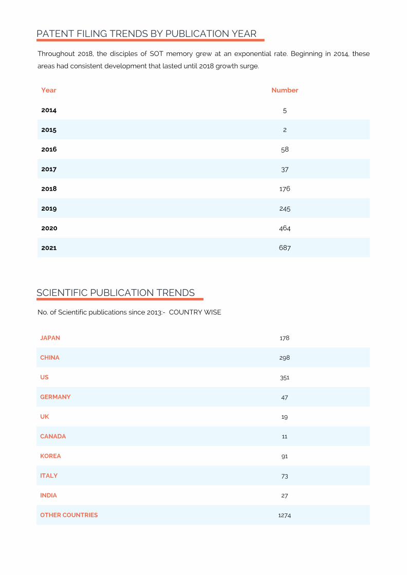
PATENT FILING TRENDS BY PUBLICATION YEAR
Throughout 2018, the disciples of SOT memory grew at an exponential rate. Beginning in 2014, these
areas had consistent development that lasted until 2018 growth surge.
Year Number
2014 5
2015 2
2016 58
2017 37
2018 176
2019 245
2020 464
2021 687
SCIENTIFIC PUBLICATION TRENDS
No. of Scientific publications since 2013:- COUNTRY WISE
JAPAN 178
CHINA 298
US 351
GERMANY 47
UK 19
CANADA 11
KOREA 91
ITALY 73
INDIA 27
OTHER COUNTRIES 1274
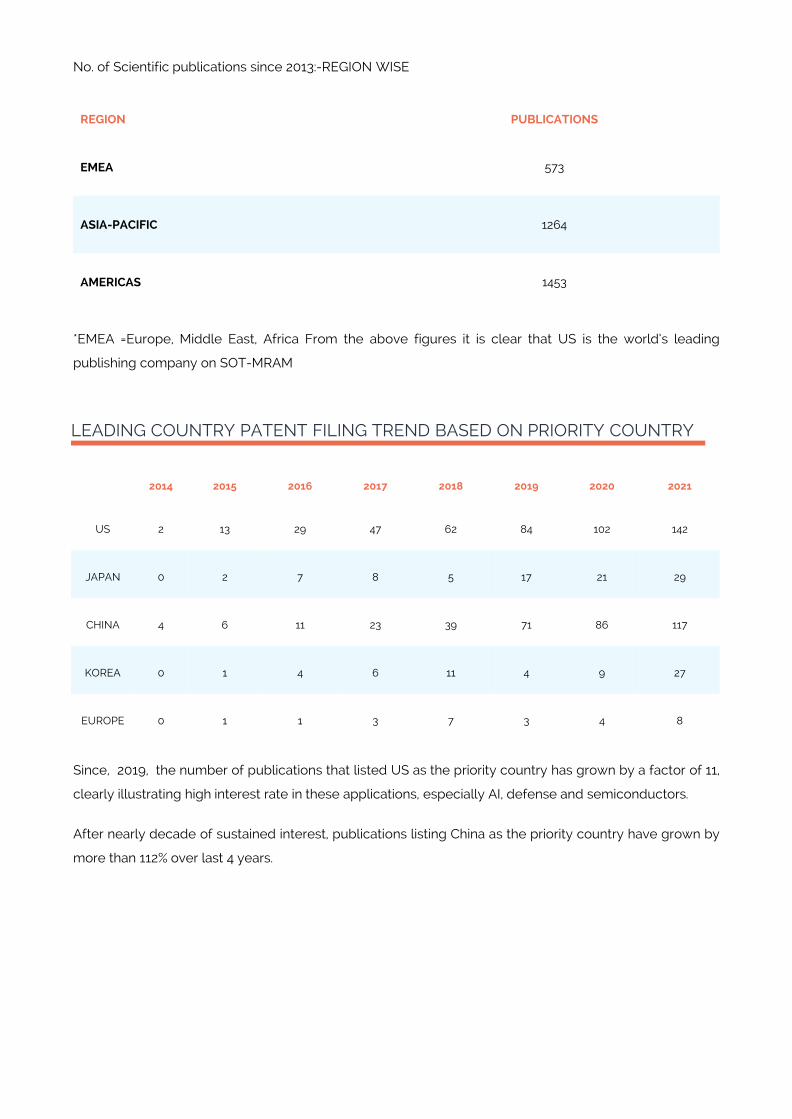
No. of Scientific publications since 2013:-REGION WISE
REGION PUBLICATIONS
EMEA 573
ASIA-PACIFIC 1264
AMERICAS 1453
*EMEA =Europe, Middle East, Africa From the above figures it is clear that US is the world’s leading
publishing company on SOT-MRAM
LEADING COUNTRY PATENT FILING TREND BASED ON PRIORITY COUNTRY
2014 2015 2016 2017 2018 2019 2020 2021
US 2 13 29 47 62 84 102 142
JAPAN 0 2 7 8 5 17 21 29
CHINA 4 6 11 23 39 71 86 117
KOREA 0 1 4 6 11 4 9 27
EUROPE 0 1 1 3 7 3 4 8
Since, 2019, the number of publications that listed US as the priority country has grown by a factor of 11,
clearly illustrating high interest rate in these applications, especially AI, defense and semiconductors.
After nearly decade of sustained interest, publications listing China as the priority country have grown by
more than 112% over last 4 years.
CONCLUSION
For shrinking technologies, non-volatile memories are promising storage technologies due to their low
static power. With the current advancements in SOT, it can be considered as a universal memory that can
easily replace all existing memories.
With commercialization of SOT-MRAM a huge evolution is expected.
SOT-MRAM Market is expected to reach US$1.8 Billion by the Year 2027, growing at a CAGR of 32.1% over
the analysis period 2020-2027.
USA is the leading market followed by China and Europe.
Among the other noteworthy geographic markets are Japan, Canada, Germany and South Korea.
In terms of incentives for innovation and allocation methods, IP rights are not the only solution, not the
best answer automatically. Even patent trolls are now seeking to take that room and, by the way, patent
lawyers worldwide are conflicting. It is therefore quite
CONNECT WITH US
Ingenious e-Brain Solutions provides high-quality, customized and cost-effective Intellectual
Property Research, Business Research and Market Research solutions to industry leaders, law firms and
innovative companies across the globe. Innovation, knowledge and transparency form the basis of our
company’s mission and vision. Along with cost benefits, we provide highest quality patent search results
ensuring fool-proof confidentiality and security. Since our inception, we have conducted patent studies
covering over 100 jurisdictions. We are an ISO certified company with offices in India and USA.
Ingenious e-Brain Solutions has a strong team of Patent Analysts with domain proficiency which is devoted
to help clients grow. Our highly qualified professionals offer tailored, value-added and cost-effective patent
services to our clients. We believe in building long term relationships with our clients who include national
and international corporations, Fortune 500 companies, world’s leading research institutes and universities as
well as independent inventors.
Copyright 2021 Ingenious e-Brain Solutions | All Rights Reserved
Email: [email protected]
Phone [IND]: +91 124 429 4218
Phone [US]: +1 347 480 2054
Phone [UK]: +44 207 193 3548
Ingenious e-Brain Solutions


