186
El tmcGRAw-HILL PUBLICATION 0 log In ex MI (1111 al xY 01111 ' 7/ I a Of 1 arc I sin I cos I tan +4, I 1/x MC I MR I M+ O 0 CI ID CI 0 II ± )os onetos c sot,
El tmcGRAw-HILL PUBLICATION
0
log In ex MI (1111 al
xY 01111
' 7/ I a Of 1
arc I sin I cos I tan
+4, I 1/x MC I MR I M+
O 0 CI
ID CI 0 II ±
)os onetos c sot,

los-ananC SOBPREPARED BYTHE EDITORS OF
Electronics
Price $5.50 U.S.A.Price $12.00 outside U.S.A.Printed in U.S.A.

All material copyrighted by
ElectronicsMcGraw-Hill, Inc.1221 Avenue of the AmericasNew York, New York 10020

CONTENTS
AMPLIFIERS
Automatic gain control quells amplifier thump 1
FET-controlled op amp permits wide dynamic range 20
Continuing biasing improves clamping amplifier 41
HP -45 calculator speeds rf amplifier design 95Digital word sets gain of amplifier 118
D -a converter forms programable gain control 121
Unity -gain stage is 50 -ohm driver 134
Combination logic cuts parts in digitally controlled amplifier 135
Two ICs make low-cost video -distribution amp 166
COMMUNICATIONS
Adjustable discriminator cleans up signal noise 9
Ordinary cassette recorder can be full-time phone monitor 15
Schottky diode pair makes an rf detector stable 25Synchronous noise blanker cleans up audio signals 34Interfacting a teletypewriter with an IC microprocessor 43Broadband p-i-n attenuator has wide input dynamic range 48Coherent phase modulation attains data rates of 100 MHz 61
Analog gate and zener diode give 70 -dB isolation at 80 MHz 64Optically coupled ringer doesn't load phone line 87ICs interface keyboard to microprocessor 90Silent timer warns of tape run -out 92
Microphone preamp gets power through signal cable 115
Optocoupler converts ac tone to digital logic levels 123
Touch Tone receiver front end provides agc and filtering 125Outputs of op -amp networks have fixed phase difference 129
Linear pot and op amp provide audio volume control 130Single preamplifier/isolator drives If and vlf receivers 133
Opto-isolators couple CRT terminals to printer lines 137Converter lets processor drive teletypewriter 142
Optical isolator circuit shows phone -line status 149
Feedback in PLL linearizes phase demodulator 151
Logic circuit selects most intense signal 155
Photocoupler provides agc for audio communications 162
Video detector stores peak for minutes 169
Mark/space modulator drives acoustic coupler 170
SIGNAL SOURCES
Sure-fire ignition system safely limits engine rpm 19Making music with IC timers 24Norton quad amplifier can be a low-cost function generator 30Generating tone bursts with only two IC timers 32Generating nanosecond pulses with TTL monostables 45Getting extra control over output periods of IC timer 57Single switch regulates number of pulses 62Generator's duty cycle stays constant under load 69Timer pulse widths range from seconds to hours 76Common silicon diodes stabilize oscillator 78Frequency divider plus op amp approximates sine wave 82Compensating the 555 timer for capacitance variations 84Antilog function generator keeps VCO output linear 93Waveform is synthesized from linear segments 97ECL IC oscillates from 10 to 50 MHz 109Monostable's pulse width is programable 112Bootstrap circuit generates high -voltage pulse train 119One-shot with feedback loop maintains constant duty cycle 122ECL tuned oscillators are voltage -stable 131
Bilateral current source is digitally programable 136Digital pulses synthesize audio sine waves 138Modified function generator yields linear VCO 141
Complementary JFETs form bimode oscillator 143Delay line in shift register speeds m -sequence generation 146Triangular waves from 555 have adjustable symmetry 160Low -distortion oscillator uses state -variable filter 165Timer IC stabilizes sawtooth generator 173
SIGNAL CONVERSION
Transistor array cuts cost of algebraic inversion 2
Two -amplifier integrator extends timing performance 18
Storing computer data with a cassette recorder 22
Switched frequency doubler provides multiple outputs 36
Full -wave rectifier needs only three matched resistors 46
Coding a -d converters for sign and magnitude 55
Rectifying wide -range signals with precision, variable gain 71
FET programs op amp for invertible gain 79
Comparator and D-MOS switch rectify small signals linearly 89
Digital command inverts signal 91
Comparator IC forms 10 -bit a -d converter 100
Pulse -frequency doubler requires no adjustment 102
Four -bit a -d converter needs no clock 167
MEASUREMENT
Winking LED notes null for IC -timer resistance bridge 17LED display shows beat frequency 42Diode pair senses differential temperature 44Window comparator needs only one op amp 53Two -component light sensor has high voltage output 55Single op amp compares bipolar voltage magnitudes 65As clipper, IC comparator is improved by feedback 67Modified window comparator compensates for temperature 75Twin oscillators form intrusion detector 81
Overvoltage indicator added to C-MOS IC tester 86Radiation monitor has linear output 94Direct -reading converter yields temperature 98Overrange indicator can enhance frequency meter 101
Tri-level indicator monitors automobile's electrical system 110Capacitive transducer senses tension in muscle fibers 117Two instrument ICs sum six inputs 124Discriminator displays first of four responses 145Logic circuit tests wiring assemblies 157Inductive proximity detector uses little power 164
FILTERS
State -variable filter uses only two op amps 15Analog filter can be programmed digitally 59Digital -to -analog converter controls active filter 80Active filter has stable notch, regulated response 175
CONTROL
Phase -locked loop adjusts to varying signal conditions 4Controlling ac loads with C-MOS bilateral switches 10SCR zero -cross trigger limits maximum load power 51
Phase -locked loop includes lock indicator 52Complementary lighting control uses few parts 73Negative feedback keeps LED intensity constant 77Buffer keeps noise from triggering thyristor 103Matched optical couplers stabilize isolation circuit 106Logic gates and LED indicate phase lock 109Phase -sequence detector trips circuit breaker 132Memdry, peripherals share microprocessor address range 147Microprocessor converts pot position to digits 150Dual -555 -timer circuit restarts microprocessor 172
DISPLAYS
PROM converts binary code to drive display 152
Graduated -scale generator calibrates data display 158
POWER SUPPLIES
Economical series regulator supplies up to 10 amperes 3
Eliminating current spiking from dc -to -dc converters 6
SCR crowbar circuit fires quickly and surely 8
IC timer makes economical automobile voltage regulator 11
Switching regulator produces constant -current output 14
Crowbar protection circuit senses load voltage directly 26
Controlled current source is versatile and precise 28
Variable voltage source has independently adjustable TC 35
Regulating supply voltage all the way down to zero 39
IC timer and voltage doubler form a dc -dc converter 50
Regulator for op amps practically powers itself 58Regulating voltage with just one quad IC and one supply 66
One -transistor regulator minimizes amplifier distortion 68Timer circuit generates precision power -on reset 68
Power -failure detector is good for short lapses 72
Regulated power supply is adjustable from 0 to 38 V 88
Power -supply add-on yields variable -ratio output 105
How to prevent spurious tripping of protection circuits 107
555 as switching regulator supplies negative voltage 108
Compact dc -dc converter yields ±15 V from +5 V 114
Oscillator drives digital clock when ac power fails 139
IC timers control dc -dc converters 144
Sensing resistor limits power -supply current 153
Controllable current source eliminates matched resistors 158
Inverting dc -dc converters require no inductors 161
LOGIC
Multiphase clock produces nonoverlapping pulses 4
External gate doubles counter speed 6
IC logic units simplify binary number conversion 21
Simple gating circuit marks both pulse edges 27
Single bipolar transistor inverts pulses on command 29
Voltage regulator protects logic pull-up transistors 31
Simplifying sum -correction logic for adding two BCD numbers 33
Electronic combination lock offers double protection 37
Serial digital multiplier handles two five -bit numbers 37
Capacitance -coupled logic fills unusual jobs 40Providing a decimal output for a calculator chip 47
IC trio converts 7 -segment code to decimal 70
Low -speed counter uses low-priced calculator chip 74
Inductor simplifies memory -driver circuit 83
Generating overlapped clock phases for CCD array 85
One NOR gate starts shift -register loop 99
Two diodes protect logic -level translator 104
Converter changes 7 -segment output to decimal or BCD 116
Two-color LED pair is digital status indicator 127
C-MOS decade divider clocks bucket -brigade delay line 127
Scope display helps debug sequential logic 154
Common -gate, common -base circuits shift voltage levels 171
SWITCHING
Transistor array converts to fast -switching thyristors 12
C-MOS touch -switch array controls analog signals 13
Attenuating transients in analog FET switches 60Latch circuits interlock remote switches electrically 78
Current and power limiter protects switching transistor 113

Automatic gain controlquells amplifier thumpby Paul BrokawAnalog Devices Inc., Semiconductor Division, Wilmington, Mass.
If an audio amplifier with automatic gain control makesa thumping noise when the input signal level changesquickly, the cause may be unwanted feedthrough of thegain control signal to the amplifier output. A simple so-lution is the addition of a resistor to prevent variationsin the control voltage from being fed through to the out-put.
In the "thumpless" agc circuit of (a), transistors Qiand Q2 form a differential amplifier that has a gain de-termined by the emitter current of the pair, IE. Thisemitter current varies the transconductance and there-fore the gain of transistors Qi and Q2. But if gainchanges too quickly, a thump may be heard. Insertingresistor R1 in the emitter -current control circuit elimi-nates the thump.
Emitter current IE is made nearly equal to the current(12) flowing through resistor R2 by using identical same -substrate transistors for Q3 and Q4. When the base -emitter voltages of these two devices are equal, theircollector currents (IE and 12) are also equal.
Since the base and collector of transistor Q4 areshorted together, this device's base -emitter voltage willrise until its collector current becomes equal to(1 - 21/3)I2, where # is the common -emitter currenttransfer ratio. Since transistor Q3 is identical to transis-tor Q4, Q3's collector current will also rise to the same
value. If current transfer ratio /3 is large and the reversevoltage feedback ratio of the transistor is small, Q3's col-lector current (IE) will nearly equal resistor current 12.The value of current 12 is:
/2 = (Econtrol VB4)1R2
where VB4 is the voltage at the base of transistor Q4.Because the collector currents of transistors Q3 and
Q4 are approximately equal, the transconductance ofthe differential pair (transistors Qi and Q2) will vary indirect proportion to the control voltage. If Qi and Q2are identical, emitter current IE will divide equally be-tween them. Each transistor will have a collector currentof aIE/2, where a is the common -base current gain.
If a is approximately equal to 1 and IE is approxi-mately equal to 12, the collector currents of transistorsQi and Q2 become:
Ici = 1C2 ge$ 1212
Ici = 1C2 (Econtrol VB4)/2R2
where Ici is the collector current of transistor Qi and 1C2the collector current of transistor Q2. The current (13)through resistor R3 is due to both resistor current Ii andcollector current Ic2. Current II, which flows through re-sistor R1, is given by:
= (E. -Econtrol)/R1
Resistor current 13 is the sum of collector current Ic2and resistor current II:
/3 = /c2 +0114E V 1 1
13 RI 2R2 (2R2 Ri)Econtrol
If RI = 2R2, the last term in this equation drops out,making current 13 independent of the control voltage,
mproved agc. Automatic -gain -control circuit (a) for audio amplifier applications eliminates unwanted thumping that may be heard when theinput -signal level changes abruptly. Resistor R1 prevents sudden variations in the control voltage from reaching the output as an audiblethumping. An audio amplifier using this agc scheme is shown in (b); amplifier gain is 30 for a control voltage of 15 volts.
1

except for a small contribution caused by the depen-dence of VB4 on Econtroi. Since the output voltage is pro-portional to resistor current 13, and not to the controlvoltage, variations in the control voltage will not be fedthrough to the output.
To implement a complete audio amplifier (b) withagc requires only a single monolithic array of fivematched transistors. Two transistor pairs are used as in-dicated in (a), while the fifth remaining transistor isused as an output signal buffer.
The base current error introduced by transistor Q4can be reduced by making resistor R2 slightly less thanwhat the half -value approximation calls for. If resistorsR1 and R2 are made variable, the performance of thecircuit can be optimized by adjusting them for min-imum feedthrough. For the component values indi-
cated, the amplifier's voltage gain is about 30 when thecontrol voltage is 15 volts. Circuit gain is directly pro-portional to the control voltage minus VB4. (Voltage VB4can be approximated as 0.55 v.)
Naturally, amplifier performance is limited by com-ponent tolerances. With components having 5% toler-ances, the feedthrough signal can typically be sup-pressed by 20 to 30 decibels. Tighter tolerances will, ofcourse, improve feedthrough suppression, but at somepoint, the various approximations made (like neglectingthe transistor base current error) will limit performance.For a large control voltage, amplifier gain becomes in-versely proportional to absolute temperature. At roomtemperature, this variation in amplifier gain amounts toabout 0.03 dB/°C, which is not objectionable for mostautomatic -gain -control applications. 0
Transistor array cuts costof algebraic inversionby Pavel GhelfanM.G. Electronics Ltd., Rehovot, Israel
Monolithic operators for algebraic inversion are conve-nient, but a reliable algebraic inverter can be built quitesimply and at less cost from an integrated five -transistorarray and two operational amplifiers. The circuit firstconverts the input signal to a logarithmic equivalentand then takes the antilog of this.
The output voltage (VL) of amplifier Al is a logarith-mic function of the input current (Iin) and the current(IR) that the transistor array sinks at pin 13:
V2kT (/R kT in( lln 1 kT ( /R2
L q VEs/ q \ /Es/ q VinlEs/
where 'ER is the emitter saturation current (with collec-tor shorted to base) of the array's transistors, k isBoltzman's constant, q is the charge of an electron, andT is absolute temperature. The antilogarithmic oper-ation is performed by amplifier A2. The circuit's outputsignal. can be expressed as:
flout = /EsRi exp(q VL/k = Ix2R1/Iin
Trimming the value of constant current In/ will adjustthe numerator of this equation so that the output volt-age of the circuit is brought to the desired value andkept there.
This inversion operator maintains good stability overa 50°C temperature range, as well as over three decadesof signal amplitude variation. Its amplitude range canbe significantly broadened by using low -bias -currentoperational amplifiers.
INPUT
40 k.S2
2
At 6
RCA CA3086
3
0.1 NF
VCC
13
12 14 10
LL
11
Ri
20 k1-2
0-11-*0.1 /IF
2
A2 6
3
OP AMPS: NATIONAL LM308
you,
Taking the reciprocal. Algebraic inverter employs IC transistor array to keep costs low and to provide good temperature stability. The circuitconverts the input signal to a logarithmic voltage and then takes the antilogarithm of this voltage to develop the output signal. The output, ofcourse, is indirectly proportional to the input and can be brought to the desired value by adjusting resistor RI.
2
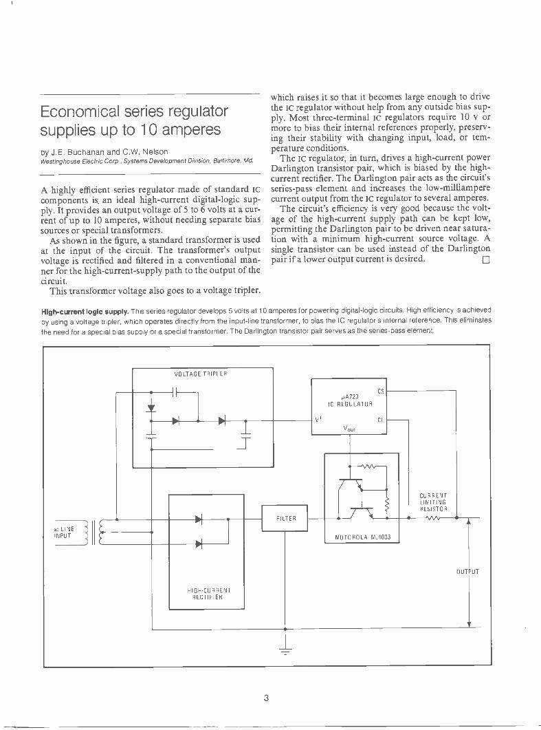
Economical series regulatorsupplies up to 10 amperesby J.E. Buchanan and C.W. NelsonWestinghouse Electric Corp., Systems Development Division, Baltimore, Md.
A highly efficient series regulator made of standard iscomponents is. an ideal high -current digital -logic sup-ply. It provides an output voltage of 5 to 6 volts at a cur-rent of up to 10 amperes, without needing separate biassources or special transformers.
As shown in the figure, a standard transformer is usedat the input of the circuit. The transformer's outputvoltage is rectified and filtered in a conventional man-ner for the high -current -supply path to the output of thecircuit.
This transformer voltage also goes to a voltage tripler,
which raises it so that it becomes large enough to drivethe is regulator without help from any outside bias sup-ply. Most three -terminal is regulators require 10 v ormore to bias their internal references properly, preserv-ing their stability with changing input, load, or tem-perature conditions.
The 1c regulator, in turn, drives a high -current powerDarlington transistor pair, which is biased by the high -current rectifier. The Darlington pair acts as the circuit'sseries -pass element and increases the low -milliamperecurrent output from the is regulator to several amperes.
The circuit's efficiency is very good because the volt-age of the high -current supply path can be kept low,permitting the Darlington pair to be driven near satura-tion with a minimum high -current source voltage. Asingle transistor can be used instead of the Darlingtonpair if a lower output current is desired.
High -current logic supply. This series regulator develops 5 volts at 10 amperes for powering digital -logic circuits. High efficiency is achievedby using a voltage tripler, which operates directly from the input -line transformer, to bias the IC regulator's internal reference. This eliminates
the need for a special bias supply or a special transformer. The Darlington transistor pair serves as the series -pass element.
LINEINPUT
VOLTAGE TRIPLER
T
HIGH CURRENTRECTIFIER
FILTER
CSµA723
IC REGULATOR
CL
vo,
CURRENTLIMITINGRESISTOR
MOTOROLA MJ4033
OUTPUT
3

CLOCK
Multiphase clock producesnonoverlapping pulsesby Glen CoersTexas Instruments, Components Group, Dallas, Texas
A multiphase clock pulse generator can be put togetherfrom a few Lc packages by taking advantage of the ver-satility of an MSI rrt decoder/demultiplexer. The clockgenerator can be programed to produce from two toseven differently phased clock -pulse trains, and none ofthe pulse edges will overlap. Furthermore, the time be-tween the pulses of the various clock phases is the sameas the width of a single pulse. This means that each in-dividual clock phase is well-defined, and there is no
pulse -edge ambiguity, as with other clock -generatingtechniques.
An MSI decade counter is used with the MSI de-coder/demultiplexer, which is connected as a three -line -to -eight -line decoder. Only three of the outputs of thedecade counter are needed.
The number of clock phases is determined by thedecoder output that is selected to reset the counter tozero. The counter's reset line is simply connected to thedecoder's output line that is next in the sequence. Asshown in the figure, a five -phase clock is produced bywiring the counter -reset line to the sixth decoder's out-put line.
The inverter at the input of the counter assures thatthe decoder is disabled when the count is changing andenabled after the data has stabilized. This eliminatesthe transients that can appear on the decoder's outputlines when the counter is changing states. 0
Programable clock. Two MSI devices-a decade counter and a three -line -to -eight -line decoder-can be wired as a simple multiphase clockgenerator. The circuit can produce from two to seven clock phases without any overlapping pulse edges. The number of clock phases is de-termined by connecting the counter's reset line to the decoder output line that is next in sequence. A five -phase clock is shown here.
ALL ICs: TEXAS INSTRUMENTS
COUNTERSN7490
CLOCK
DECODERSN74155
01
02
03
04
05
0
CLOCK
01
02
03
04
05
Phase -locked loop adjusts tovarying signal conditionsby Charles A. WatsonE-Systems Inc., Greenville, Texas
In many phase -locked receivers, the gain of the ampli-fier in the phase -locked loop must be changed to adaptthe loop gain to varying signal conditions. If the ampli-fier's gain and offset voltage are changed simulta-neously, the signal -acquisition time can be shortened,and signal-to-noise ratios can be optimized.
When the entire loop, including the phase detector,
operates from a single supply, the output of the phasedetector must be other than zero to have the vco rest atits midrange frequency. If not of the proper magnitude,this nonzero output offsets or even saturates the loopamplifier, driving the vco to some non -midrange fre-quency.
Therefore, an offset voltge, which permits the loop tobe adjusted for a midrange vco rest frequency, is usu-ally introduced at the loop amplifier. If the loop ampli-fier's gain must be changed to accommodate varying in-put -signal conditions, this offset voltage must also bechanged to maintain the same vco midrange frequency.
The figure contains a block diagram of a phase -locked loop (a) that includes a switched -gain amplifier,which provides offset compensation for the loop ampli-fier in response to remotely commanded gain adjust -
4
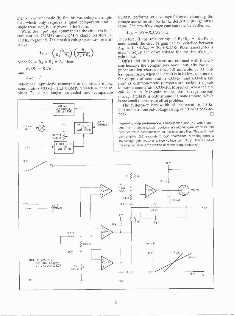
ments. The schematic (b) fQr this variable -gain ampli-fier, which only requires a quad comparator and asingle transistor, is also given in the figure.
When the input logic command to the circuit is high,comparators COMP]. and COMP2 clamp resistorsand R2 to ground. The circuit's voltage gain can be writ-ten as:
A°(i) = (RIR-F1R3) (R2R+4R4)
Since R1 = R2 = R3 = R4, then:
R4/R2 = R3/RIand:
A v(1) = 1
When the input -logic command to the circuit is low,comparators COMP]. and COMP2 unlatch so that re-sistor R1 is no longer grounded and comparator
SIGNALINPUT
10 V -
0 V
5V
0 V -
VOLTAGE -CONTROLLEDOSCILLATOR
OFFSETADJUST
V,,
+v
LOOP FILTERAND
AMPLIFIER
SWITCHED -GAIN
AMPLIFIER
LOGICCOMMAND
LOGICCOMMANDIN
QUAD COMPARATOR:NATIONAL LM339 orMOTOROLA MC3302P
b)
COMP3 performs as a voltage -follower, clamping thevoltage across resistor R2 to the desired midrange offsetvalue. The circuit's voltage gain can now be written as:
A°(o) = (R2 + R4)/R2 = 2
Therefore, if the relationship of R4/R2 = R3/111 ismaintained, the circuit's gain can be switched betweenAva) = 1 and Avo = (R2 + R4)/R2. Potentiometer R5 isused to adjust the offset voltage for the circuit's high -gain mode.
Offset and drift problems are minimal with this cir-cuit because the comparators have unusually low out-put -saturation characteristics (10 millivolts at 0.1 mil-liampere). Also, when the circuit is in its low -gain mode,the outputs of comparators COMP]. and COMP2 ap-pear as common -mode (temperature -tracking) signalsto output comparator COMP4. Moreover, when the cir-cuit is in its high -gain mode, the leakage currentthrough COMP]. is only around 0.1 nanoampere, whichis too small to create an offset problem.
The full -power bandwidth of the circuit is 10 ki-lohertz for an output -voltage swing of 10 volts peak -to -peak. CI
Improving loop performance. Phase -locked loop (a), which oper-ates from a single supply, contains a switched -gain amplifier thatprovides offset compensation for the loop amplifier. This switched -gain amplifier (b) responds to logic commands, providing either alow -voltage gain (kw) or a high voltage gain (A,10)). The output ofthe loop oscillator is maintained at its midrange frequency.
15V
5
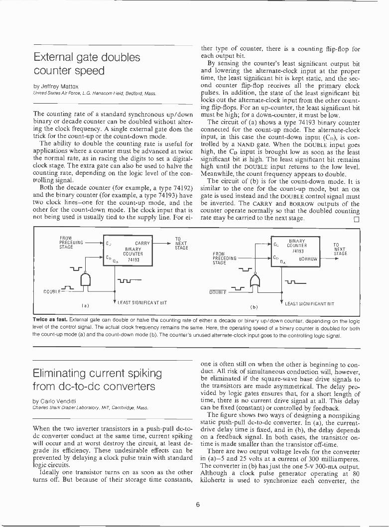
External gate doublescounter speedby Jeffrey MattoxUnited States Air Force, L.G. Hanscom Field, Bedford, Mass.
The counting rate of a standard synchronous up/downbinary or decade counter can be doubled without alter-ing the clock frequency. A single external gate does thetrick for the count -up or the count -down mode.
The ability to double the counting rate is useful forapplications where a counter must be advanced at twicethe normal rate, as in racing the digits to set a digital-clock stage. The extra gate can also be used to halve thecounting rate, depending on the logic level of the con-trolling signal.
Both the decade counter (for example, a type 74192)and the binary counter (for example, a type 74193) havetwo clock lines-one for the count -up mode, and theother for the count -down mode. The clock input that isnot being used is usually tied to the supply line. For ei-
ther type of counter, there is a counting flip-flop foreach output bit.
By sensing the counter's least significant output bitand lowering the alternate -clock input at the propertime, the least significant bit is kept static, and the sec-ond counter flip-flop receives all the primary clockpulses. In addition, the state of the least significant bitlocks out the alternate -clock input from the other count-ing flip-flops. For an up -counter, the least significant bitmust be high; for a down -counter, it must be low.
The circuit of (a) shows a type 74193 binary counterconnected for the count -up mode. The alternate -clockinput, in this case the count -down input (CD), is con-trolled by a NAND gate. When the DOUBLE input goeshigh, the CD input is brought low as soon as the leastsignificant bit is high. The least significant bit remainshigh until the DOUBLE input returns to the low level.Meanwhile, the count frequency appears to double.
The circuit of (b) is for the count -down mode. It issimilar to the one for the count -up mode, but an oRgate is used instead and the DOUBLE control signal mustbe inverted. The CARRY and BORROW outputs of thecounter operate normally so that the doubled countingrate may be carried to the next stage.
FROMPRECEDINGSTAGE
DOUBLE
(a)
Cu
Co
TONEXT
BINARYCARRY Cu COUNTER TO
STAGEBINARYCOUNTER FROM
74193 NEXTSTAGE
74193 CD BORROWOA
PRECEDINGSTAGE
LEAST SIGNIFICANT BIT
DOUBLE
(b)LEAST SIGNIFICANT BIT
Twice as fast. External gate can double or halve the counting rate of either a decade or binary up/down counter, depending on the logiclevel of the control signal. The actual clock frequency remains the same. Here, the operating speed of a binary counter is doubled for boththe count -up mode (a) and the count -down mode (b). The counter's unused alternate -clock input goes to the controlling logic signal.
Eliminating current spikingfrom dc -to -dc convertersby Carlo VendittiCharles Stark Draper Laboratory, MIT, Cambridge, Mass.
When the two inverter transistors in a push-pull dc -to -dc converter conduct at the same time, current spikingwill occur and at worst destroy the circuit, at least de-grade its efficiency. These undesirable effects can beprevented by delaying a clock pulse train with standardlogic circuits.
Ideally one transistor turns on as soon as the otherturns off. But because of their storage time constants,
one is often still on when the other is beginning to con-duct. All risk of simultaneous conduction will, however,be eliminated if the square -wave base drive signals tothe transistors are made asymmetrical. The delay pro-vided by logic gates ensures that, for a short length oftime, there is no current drive signal at all. This delaycan be fixed (constant) or controlled by feedback.
The figure shows two ways of designing a nonspikingstatic push-pull dc -to -dc converter. In (a), the current-drive delay time is fixed, and in (b), the delay dependson a feedback signal. In both cases, the transistor on -time is made smaller than the transistor off -time.
There are two output voltage levels for the converterin (a)-5 and 25 volts at a current of 300 milliamperes.The converter in (b) has just the one 5-v 300-mA output.Although a clock pulse generator operating at 80kilohertz is used to synchronize each converter, the
6

(a)
CLOCKa
s a
T
C O
0FF2
S
C
043 E2.. re a
1*_ 2N3421
O
FF1,FF2: MOTOROLA MC 945F NAND GATES: 7400BUFFERS: 7440
H 14- 2 ,usCLOCK
-0112.5 As
VA
VB
(b)
2 µs
25µs
7493 --A.
CLOCK
4 -BITBINARY
COUNTER
INPUT Row
CLOCK
CC
J_ 25 V
I =
,,,
n re... D I -2N3421 E
VC
VD
VE
VF
4352
26 TURNS
108 TURNS
7-108 TURNS
OUTPUT+I- 5V,/k\300 mA
115 µF(30V)
OUTPUT25 V,300 mA
25 µF(50V)
DIODES: UNITRODE UTX2107
TRANSFORMER:CORE, MAGNETICS INC.,50000-1F; WIRE SIZE, AWG #32
I
1-4-- 27 µs -401
I
2
1-4- 25 As --0-1
rL-
-
0
NANO GATES: 7400BUFFERS: 7440TRANSFORMER: SAME AS IN (a)DIODES: SAME AS IN (a)
2µs
-P112.5014-
VA1.0- 25 µs-o.1
Vs LI
VD1
VD
0I..
s
CS.co
A 43 S2>oj
(.12)
43 E2
01
2N3421
25 V
2N3421
600 E2
300 E2 1N914
Oi
600 E2
300 E2
OUTPUT5 V,300 mA
J.15 µF
(30V)
1N914
VE --1
VF
vG _1
V H
Improving dc -dc converter efficiency. These dc -dc converters employ push-pull inverter transistors that switch at 20 kilohertz. Conven-ional digital ICs are used to delay the drive signals to the switching transistors so that these devices cannot conduct simultaneously, causingunwanted current spikes. The converter in (a) has a fixed delay, while the delay of the converter in (b) depends on a feedback signal voltage.
switching frequency is only 20 kHz in each case, and thenominal transistor on/off time is 25 microseconds (totalperiod of 50 us).
In the fixed -delay circuit of (a), flip-flops FFi andFF2 generate the basic square -wave drive for transistorsQi and Q2. The flip-flops divide the clock frequencydown from 80 to 20 kilohertz, and the NAND gates pro-vide the delays for the transistor drive signals.
The resulting asymmetrical driving waveforms havean on -time of 23 us and an off -time of 27 [Ls. This means
that each transistor experiences a 2 -us delay in its drivesignal. For the transistors used here, this delay preventscurrent from flowing into the transformer primary for0.5 [Ls. The width of the delay pulse (2 us here) is toowide if the converter's output ripple voltage increasesand too narrow if there is no deadband for the trans-former primary current.
In the feedback -adjusted -delay circuit of (b), a binarycounter, rather than flip-flops, divides the clock fre-quency down to 20 kHz. NAND gates again provide the
7
appropriate delays for producing asymmetrical transis-tor drive signals.
The feedback voltage, which is taken from the trans-former secondary, determines when the transistors turnon, while the reference voltage from the counter outputdetermines when they turn off. To delay the turn -onfeedback signal properly, the storage time of the recti-
fier diodes, as well as the flux flyback time of the trans-former, must be taken into account. For circuit (b), thedeadband time is 0.3 its.
BIBLIOGRAPHYAlphonso H. Marsh, "Gating Scheme Maximizes dc -dc Converter Efficiency," Electronic
Design, June 22, 1972. p. 100.Robert F. Downs, "Minimize Overlap to Maximize Efficiency in Saturated Push-pull Cir-cuits," EDN/ EEE. Feb. 1, 1972, pp. 48-50.
SCR crowbar circuitfires quickly and surelyby Steve SummerHauppauge, N.Y.
A monolithic voltage regulator's presence in an SCRcrowbar circuit makes the circuit fast -acting, depend-able, and capable of producing fast-risetime drive cur-rents as large as several amperes. The circuit shown inthe diagram is simple yet effective, providing a drivecurrent of 200 milliamperes with a risetime of 1 micro-second. The 723 -type IC regulator is used as a compara-tor that contains its own stable reference voltage source.The setpoint of the comparator establishes the protec-tion voltage level for the power -supply bus.
A satisfactory crowbar circuit for good power -supplyprotection generally asks a lot of the crowbar SCR. Typi-cally, power supplies have large output capacitancesthat impose high surge currents and di/dt levels on thecrowbar SCR when it is fired. These large current surgescan cause SCR failure or degradation if the SCR drivecurrent is inadequate or soft (has a slow risetime).
The gate drive required to attain the SCR's specifiedsurge and di/dt capability may be many times greaterthan the worst -case gate drive needed for turn -on. In
addition, for best di/dt resistance, the risetime of thegate drive should be quite short, preferably less than amicrosecond.
Many simple crowbar circuits use such devices aszener diodes to fire the crowbar SCR. Although this re-sults in a soft turn -on that will fire the SCR at least once,the dependability of such a scheme is questionable.
The circuit shown, however, is hard -firing. ResistorsR1 and R2 make up a voltage divider that nominallysets the voltage at the inverting input of the comparatorto 2 volts. Another voltage divider, consisting of resis-tors R3 and R4, samples the power -supply bus anddrives the comparator's noninverting input. When thevoltage on the power -supply bus exceeds the setpoint ofthe comparator, the output of the regulator rises. Thisvoltage rise, which appears across resistor R5, adds (inphase) to the voltage at the comparator's noninvertinginput, providing rapid regeneration, as well as a fast -rising pulse to drive the SCR.
Resistor R6 limits the SCR drive current to about 200milliamperes, a value that is adequate for sensitive -gateor amplifying -gate devices. To obtain larger drive cur-rents of up to several amperes, an emitter -follower stagecan be added at the output of the regulator. The capaci-tor acts as a filter to prevent the crowbar from firing inresponse to transient voltages.
VOLTAGE REGULATOR
PROTECTED SUPPLY BUS
REF,7 15 V
10
COMPARATORR6
3.352
R R2
µA723
33 E2
SCR
Hard -firing SCR. Crowbar protection circuit employs an IC voltage regulator to produce a fast-risetime large -value gate drive current for theSCR. The regulator, which is used as a comparator, has its own voltage reference source. When the voltage on the power -supply bus ex-ceeds the set point of the comparator, the regulator's output voltage increases, producing a large fast -rising pulse that fires the SCR.
8

Adjustable discriminatorcleans up signal noiseby Dennis D. BarberUniversity of Houston, Houston, Texas
Telemetry signals or other logic signals often pick up alot of extra noise during transmission. But they can eas-ily be cleaned up at the receiving end by a discriminatorcircuit having adjustable hysteresis.
The voltage discriminator shown in the figure canclean up signals containing as much as 70% noise with-out the need to alter the signal amplitude or dc level.The input to the amplifier that serves as the voltage -dis-criminator (amplifier A4) is kept constant at 5 voltspeak -to -peak. But the signal to be conditioned, the oneat the input to the circuit, does not have to be criticallymaintained or its level known precisely.
Amplifier Al is gain -controlled, with field-effect tran-
sistor Qi acting as the gain -control element. This FET,which functions as a voltage -variable resistor, is con-trolled by amplifiers A2 and A3. Amplifier A4 is the volt-age -discriminator stage that provides the adjustablehysteresis through its variable regenerative feedback.
Before the capacitively coupled input signal goespositive or negative, the output of amplifier Al may betreated as if it were at ground. The gain of amplifier Alis then at its maximum since the inputs to amplifiers A2and A3 are below (in absolute magnitude) their respec-tive reference voltages. The output of each amplifier isnow positive, and diodes D1 and D2 are back -biased,which allows transistor Qi to turn fully on.
If the input signal goes positive, the output of Al willmove towards the positive power -supply level. When itreaches the reference voltage of A2, the output of A2quickly swings negative, turning transistor Qi partiallyoff and thus lowering the gain of Al. The output of Al isheld at the positive reference voltage until this referencelevel is greaten than the input voltage multiplied by themaximum gain of Al. At this point, the input voltage isonly a few millivolts above ground.
100µF 100µF8.2 kS2
INPUT
100 kS2
OP AMPS: 741DIODES: 1N914
0.001
I
a,2N3819
+10 V
8.2'1(2--Ws"--
00.03µF
100 kS2
A2r 10 kS2
+REF
- REF
A3 4.10 KE2 =7-
+
10
10 kS2
10 kS2
-10 V
4.7 k1.
LOGIC SUPPLY
OUTPUT
203565
NOISE
SIGNAL 7
MIVIMMWMWM
immommommmMEMMOMMEWMMMEMMENEMM
2 ms/cliv
SIGNAL+NOISE >
OUTPUT -3.-
i,
111111777764 ii0A;"7kdaAg111AMLIwAIMMIMMUMMOMM111101111
2 ms/div
Pulling the data out of the noise. Adjustable -hysteresis voltage discriminator makes significant improvement in signal-to-noise ratios, as canbe seen from the scope traces. The level of regenerative feedback of amplifier A4, the voltage -discriminator stage, is adjusted to provide opti-mum noise immunity. The gain of amplifier Al is controlled by transistor Q1, which is operated as a voltage -variable resistor.
9
As the input signal swings from positive to negative,the output of amplifier A2 goes positive, but the outputof amplifier A3 becomes negative. The gain of amplifierA1, therefore, is limited until the input signal again re-turns to very near ground.
In this way, the input voltage to amplifier A4, thevoltage discriminator, is maintained at a constant level.The threshold voltages for A4 can be set slightly lessthan the reference voltages of A2 and A3, enabling thecircuit to provide excellent noise immunity.
The capacitors at the input of the circuit are used tolimit the amplitude of high -frequency spikes. The 100-microfarad capacitor values indicated in the diagramfunction well over a frequency range of 1 cycle per min-
ute to 1,000 cycles per second and over an input ampli-tude range of 1 to 10 v pk-pk.
Transistor Qi can be almost any junction FET. Tran-sistor Q2 is included to make the output of the circuitcompatible with the type of logic being used. Manytypes of general-purpose op amps should work in thecircuit, and even Norton amplifiers like the type -3900units can probably be used if the appropriate circuitmodifications are made.
The oscilloscope photographs show how dramaticallythis discriminator can clean up signals. One photoshows separate signal and noise voltages, while theother photo shows the total input signal and the result-ing output.
Controlling ac loads withC-MOS bilateral switchesby Arthur JohnsonDarlington, Md.
Power to an ac load can be efficiently controlled by anintegrated complementary-Mos quad bilateral switchand a capacitively triggered sensitive -gate triac. Thenecessary gate -triggering current comes, not from thelow -voltage C-MOS power supply, but from the ac line.
Capacitor -triggering is best for firing the triac be-cause it produces the maximum current (at 90° phaseshift) when the ac voltage crosses the zero -voltage level.Therefore, the fullest possible use is made of gate -trig-gering current. Also, the triac is switched into conduc-tion at a low voltage to reduce switching transients, andmaximum power is delivered to the load.
The driver circuit for ac loads is drawn in the dia-
Ac-load driver circuit. C-MOS bilateral switches are used to capaci-tively trigger a sensitive -gate triac that can carry up to 1 ampere. Tokeep switching transients to a minimum, the triac is fired at a lowvoltage derived from the ac line. The series switch provides isolationto prevent false triggering of the triac, while the shunt switch protectsthe series switch from possibly damaging high voltages.
gram. Because the on -resistance of each c-mos bilateralswitch is several hundred ohms, circuit voltages couldfalsely trigger the triac. The triac gate therefore needs tobe isolated by the series switch, which, in turn, needs tobe protected in its nonconducting state by the shuntswitch from possibly damaging high voltages.
Two power -supply voltages, +7.5 volts and -7.5 v,are needed to control both positive and negative ac volt-age excursions. This may prove to be a minor inconven-ience. But since the necessary gate -triggering currentdoes not have to come from these supplies, they may besimple half -wave -rectified high -resistance sources.
The sensitive -gate triac used here has a maximumcurrent -carrying capacity of 1 ampere. If a larger loadmust be handled, a triac with higher ratings can be con-trolled by the smaller triac. In this way, a large load canbe controlled without wasting a large amount of energy.
The capacitor value is chosen to provide the requiredtriac-triggering current of 5 milliamperes maximum:
C = (5 mA)/2TrfEin.where f is the ac frequency and emax is the zero -to -peakac voltage level. 0
INPUT
+7.5 V
100 Ic.L
0r-1111
INVERTER-7-N-1 SWITCH
120 Vac
- 0.1 NF
SHUNT(SWITCH O T
SERIES L__JSWITCH
-7.5 V
10
10 kS2
ac
LOAD
TRIAC2N6071A
C-MOS QUAD BILATERAL SWITCH:RCA CD4016A OR EQUIVALENT
10
'NY

IC timer makes economicalautomobile voltage regulatorby T.J. FusarPowell -Mac Electronics, Madison, Wis.
A 555 -type is timer, in combination with a power Dar-lington transistor pair, can provide low-cost automotivevoltage regulation. Such a regulator can even make iteasier to start a car in cold weather.
As the diagram shows, the circuit requires very fewparts. The value of resistor R1 is chosen to prevent thetimer's quiescent current, when the timer is off (output,pin 3, low), from turning on the Darlington pair.
If battery voltage becomes too low, the timer turnson, driving its output high and drawing a current ofabout 60 milliamperes through resistor R2. This causesa sufficient biasing voltage to be developed across re-sistor R1 and the Darlington turns on, supplying theenergizing current to the field coil of the car's alternator.Diode D1 suppresses the reverse voltage of the field coilwhen the Darlington pair is turned off.
The regulator's low -voltage turn -on point is fixed bysetting the voltage at the timer's trigger input (pin 2) toapproximately half the reference voltage existing at itscontrol -voltage input (pin 5). The high -voltage turn-offpoint is set by making the voltage at the timer'sthreshold input (pin 6) equal to the reference voltage atpin 5. At 77°F, the turn -on voltage is typically 14.4volts, and the turn-off voltage is typically 14.9 v. Thesevoltage levels, of course, should be set to match thecharging requirement of a given car's specific battery -alternator combination.
The value of the reference voltage is established bythe diode string, D2 through D5; here, it is approxi-mately 5.9 v. The output voltage has a negative tem-perature coefficient of -11 millivolts/°F.
A transistor and a couple of resistors can be added tothe circuit for better cold -weather starting. These partsare drawn in color in the figure. During starting, thetransistor holds the timer in its off state, lightening theload on the car's cranking motor. (And to prevent radiointerference, a 10-microfarad capacitor can be con-nected from the Darlington emitter to ground.)
Regulating car voltage cheaply. MOnolithic 555 -type timer is the heart of this simple automobile voltage regulator. When the timer is off so
that its output (pin 3) is low, the power Darlington transistor pair is also off. If battery voltage becomes too low (less than 14.4 volts in thiscase), the timer turns on and the Darlington pair conducts. The parts drawn in color permit easier starting in cold weather.
TURN ONADJUST
20 kS2
TO COIL TERMINALON STARTER RELAYFROM IGNITION SWITCH
2.21(12
TO BATTERY ANDALTERNATOR OUTPUTVIA FIELD RELAY ANDIGNITION SWITCH
20 kS2
TURN-OFFADJUST
Ri
68 .S-2 2.2 kS2
0.01µF
2.2 kS
0.01mF
8
6 5
SIGNETICS
NE555
TIMER1x
2N5720"
R2
180E2(2 W)
Z 02S. 03
X 04
'31-' D51N5229
1N914*
POWERDARLINGTONMOTOROLAMJE1090
TO ALTERNATORFIELD COIL
Dl1N4001
* CAN BE ANY GENERAL-PURPOSESILICON DIODES OR 1N4157 DEVICE
** CAN BE ANY GENERAL-PURPOSESILICON TRANSISTOR
11
Transistor array converts tofast -switching thyristorsby H.S. KothariCentral Electronics Engineering Research Institute, Pilani, India
An ordinary monolithic transistor array can be wired toperform as multiple four -layer silicon -controlledswitches by making use of the terminal to the array'ssubstrate. For example, a seven -transistor array havingcommon emitters can be used to implement a seven -stage ring counter.
As shown in (a), the npn transistor array has a sepa-rate connection to its p -type substrate. The array is eas-ily wired as shown in (b), with the substrate being em-ployed as a common anode to form pnpn structures thatcan be regarded as silicon -controlled switches. Andsince the geometry of each transistor is very small,switching times can be on the order of a few nano-seconds.
The schematic of the ring counter is drawn in (c). Thefirst stage is turned on by the trailing edge of the resetpulse. Now, when a clock pulse is applied to the inputtransistor, the voltage at this transistor's collector drops,and the other counter stages are turned off. In this way,a trigger pulse is transferred from the first stage to thesecond stage. The next clock pulse causes a trigger pulseto go from the second to the third stage. This processcontinues and repeats when the seventh counter stagetriggers on the first counter stage.
The hold -on current for any stage can be between 50microamperes and 1 milliampere. The negative voltageamplitude of the reset pulse should be large enough tolower the voltage of the anode gate of the first stage sothat this stage is sure to fire. The anode -gate voltage,therefore, is made negative with respect to the anodevoltage.
The length of the triggering delay is determined bythe capacitance value selected. Voltage amplitudes canbe made as large as the collector -emitter breakdownlimit of each transistor by increasing the supply voltage,as well as the zener voltage, to some suitable maximumlevel.
Wiring transistors as thyristors. Integrated seven -transistor array (a) can be wired as silicon -controlled switches by making use of theircommon substrate connection. The transistors can then be operated as four -layer devices (b) that have switching times on the order of a fewnanoseconds. One application for the pnpn switch array is illustrated in (c)-a seven -stage ring counter.
12

C-MOS touch -switch arraycontrols analog signalsby Max W. HauserBerkeley, Calif.
A few inexpensive complementary-mos ICs can be usedto create a bounceless buttonless touch -switch array.The resulting switching circuit takes advantage of theextremely high input impedance of c-mos devices to de-tect the ambient signals (electrostatic charge and power -line hum) present on a person's finger. The circuit's out-puts are solid-state switches that are capable of control-ling audio or analog signals with negligible distortionand that, in many cases, are compatible with existingcircuitry. Light -emitting diodes provide a visual displayof the current state of these switches.
The heart of each touch -switch (a) is a set -reset flip-flop (one -quarter of a quad latch) whose inputs arebiased to the VDD supply through 22-megohm resistors.Under normal (resting) conditions, this renders the in-puts inactive, and the flip-flop retains its last state.When a finger or large conductive object touches eitherthe on or off input, a noise voltage appears across thebias resistor at that input and is amplified through theregenerative action of the flip-flop. This sets the flip-flopto the desired output state, where it remains until resetby touching the other input.
The flip-flop's output simultaneously controls ananalog switch and a buffer/inverter that drives a panel -mounted LED. The output from the buffer can also beused to activate a Tn. input, provided that the internalpull-up supply (Vcc) is made equal to the TTL power -supply voltage. The 100-kilohm resistor and the 0.1-mi-crofarad capacitor serve to decouple the VDD bias sup-ply so that there is no interaction between the input anddisplay portions of the circuit.
The block diagram (b) shows how a quadruple touch -switch array looks. The touch -sensors should be smallmetal plates-squares or disks having a side or diameterof 1 to 2 centimeters are best. A substantial increase inplate area results in a proportionate increase in thequiescent hum pickup, and can reduce circuit reliabilityunless the sensor is mounted very carefully. At the ex-pense of added construction complexity, the nos ortheir mountings can be given a conductive coating, per-mitting them to serve as the solid-state equivalent of il-luminated push-button switches.
Type-CD4016 analog switches work well for noncriti-cal applications, for example, if the circuit is to be usedas a source selector for an audio -mixing console. Inmore critical systems, however, it may be desirable tosubstitute lower -impedance devices, such as type-CD4066 units. Of course, each flip-flop output can drivemany analog switches, and a complex switching ar-rangement can be created that might be difficult or un-economical to implement with mechanical devices. Nor-mally closed switching is possible by driving the analogswitches with the buffer/inverter outputs, but the cir-
Touch-actuated switching. A simple touch -switch (a) can be built with complementary-MOS ICs. The high input impedance of the C-MOSlatch permits the ambient signals of a fingertip to be sensed. The latch's output then controls a C-MOS analog switch, which implements thedesired switching function. The LED indicates whether this analog switch is on or off. A quadruple touch -switch array is shown in (b).
PROTECTION RESISTORS
56 k12
TOUCHINPUTS{
ON
56k12OFF 0-Vvs.,
+VDD
(8-15 V)
(a)
INPUT -BIASINGNETWORK
LATCH
TOUCHPOINTS
( b)
22 ma
100 ki2
a
ANALOG SWITCH
22 MS2
BIAS BUS
0.1 µF(50 VI
LATCHES
330 (V = +5 V)820 521V = VDD)
NoW
TT L OUTPUT(OPTIONAL)
ANALOG SWITCHESAND LEO DRIVERS
Cr
n
0
SWITCHCONTACTS
0
'\D
Or0
0
0
LED
= VDD OR +5 V(FOR TTL INTERFACE)
LED SUPPLY BUS
25µF (20 V)
C-MOS ICs: RCA OR EQUIVALENTLATCHES: CD4044BUFFER/INVERTERS: CD4009ANALOG SWITCHES: CD4016LEDs: LITRONIX RL-2RESISTORS: Y.W, 5%
SWITCHCONTACTS
13
cuit's TTL interface must be sacrificed.In remote locations, where power lines or other major
electromagnetic -field sources are not available, it is ad-visable to install a second contact (at ground potential)on each sensor, so that a slight conduction between the
two contacts will assure triggering. Also, to eliminateany chance of damage to the flip-flop inputs from an ex-ternal power source, the inputs should be protectedagainst excessive current flow with 56-kilohm resistors,as shown. 0
Switching regulator producesconstant -current outputby Steven E. SummerHauppauge, N.Y.
The high efficiency that can be achieved with switchingregulators need not be restricted solely to voltage regu-lators. By taking advantage of the convenience of amonolithic voltage regulator, a free -running constant -current switching regulator having a 1 -ampere outputcan be built for applications like battery charging.
A 723 -type IC regulator acts as the circuit's referenceand comparator. The ic's 7.15 -volt internal reference isscaled to approximately 3 v by the voltage dividerformed by resistors R1 and R2. These resistors also feedthe ic's noninverting input, while resistors R3 and R4drive the IC's inverting input. The lower end of resistorR4 is connected to shunt resistor R5, and approximately
1 v appears across this shunt when the ic's comparatorterminals are nearly balanced.
A hysteresis voltage of around 28 millivolts is appliedto the ic's noninverting input through resistor R6. Thissets the minimum output ripple of the circuit at 28 mil-liamperes peak to peak. But if the storage time of out-put transistor Qi is significant, the ripple current will behigher.
When the circuit's feedback loop calls for a currentincrease, the output stage of the IC regulator conductsand a current pulse of 12 mA flows into the Vc terminal.(The size of the current pulse is determined by resistorR7.) This current pulse drives transistor Qi.
The zener diode (Di) is used to bias the output stageof the IC regulator, while the junction diode (D2) oper-ates as a freewheeling diode. Inductor L1 and capacitorCl filter the switched waveform. The circuit's maximumoperating frequency depends on the size of the load andis typically 20 kilohertz. 0
Constant -current source. Switching regulator circuit provides a 1 -ampere constant -current output that has a peak -to -peak ripple of 28 mil-liamperes. The integrated 723 -type voltage regulator functions as a reference source and a comparator. Transistor 01 is a current booster,while inductor L1 and capacitor C1 filter the switched waveform. The circuit's operating frequency can be as high as 20 kilohertz.
4.12 k.S2
2 kS2
+ 28 V
1.4A723
3.3 kn
4.12 1(12.
3 kst
Vc
REF VouT
INV
LIMIT
VOLTAGEREGULATOR
NONINV SENSE
R7
47 S2
DI
1N746
co01
MOTOROLA MJ2500
L, 12 mH
1N4942
200pFOUTPUT
14
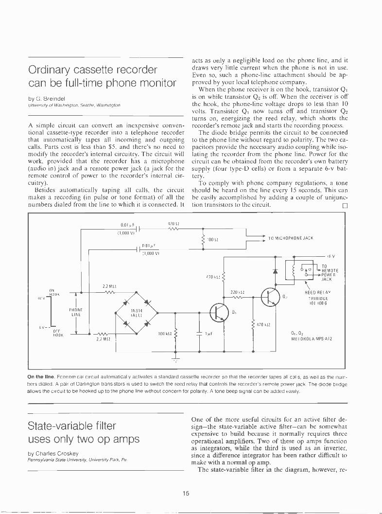
Ordinary cassette recordercan be full-time phone monitorby G. BreindelUniversity of Washington, Seattle, Washington
A simple circuit can convert an inexpensive conven-tional cassette -type recorder into a telephone recorderthat automatically tapes all incoming and outgoingcalls. Parts cost is less than $5, and there's no need tomodify the recorder's internal circuitry. The circuit willwork, provided that the recorder has a microphone(audio in) jack and a remote power jack (a jack for theremote control of power to the recorder's internal cir-cuitry).
Besides automatically taping all calls, the circuitmakes a recording (in pulse or tone format) of all thenumbers dialed from the line to which it is connected. It
acts as only a negligible load on the phone line, and itdraws very little current when the phone is not in use.Even so, such a phone -line attachment should be ap-proved by your local telephone company.
When the phone receiver is on the hook, transistor Qiis on while transistor Q2 is off. When the receiver is offthe hook, the phone -line voltage drops to less than 10volts. Transistor Qi now turns off and transistor Q2turns on, energizing the reed relay, which shorts therecorder's remote jack and starts the recording process.
The diode bridge permits the circuit to be connectedto the phone line without regard to polarity. The two ca-pacitors provide the necessary audio coupling while iso-lating the recorder from the phone line. Power for thecircuit can be obtained from the recorder's own batterysupply (four type -D cells) or from a separate 6-v bat-tery.
To comply with phone company regulations, a toneshould be heard on the line every 15 seconds. This canbe easily accomplished by adding a couple of unijunc-tion transistors to the circuit.
( NHOOK
fill V
6 V- -OFFHOOK
0.010F 470 S2
(1,000 V)
2.2 MS2
PHONELINE
2.2 MS'
0.01 pF
(1,000 V)
470 kS2
100 kS2
TO MICROPHONE JACK
220 kS2
1 pF
U.
LTDREMOTE
POWERJACK
REED RELAY
TRIRIDGE101 100 6
D,, Q2.MOTOROLA MPS Al2
On the line. Economical circuit automatically activates a standard cassette recorder so that the recorder tapes all calls, as well as the num-bers dialed. A pair of Darlington transistors is used to switch the reed relay that controls the recorder's remote power lack. The diode bridgeallows the circuit to be hooked up to the phone line without concern for polarity. A tone beep signal can be added easily.
State -variable filteruses only two op ampsby Charles CroskeyPennsylvania State University, University Park, Pa.
One of the more useful circuits for an active filter de-sign-the state -variable active filter-can be somewhatexpensive to build because it normally requires threeoperational amplifiers. Two of these op amps functionas integrators, while the third is used as an inverter,since a difference integrator has been rather difficult tomake with a normal op amp.
The state -variable filter in the diagram, however, re -
15

quires only two op amps. The circuit takes advantage ofthe recently introduced integrated quad amplifiers, such 500
as Motorola's MC340I and National's LM3900, whichrespond to a current difference instead of a voltage dif-ference. Such amplifiers permit a difference integratorto be built simply.
The center frequency of the filter's bandpass functionis still determined by the usual relationship of:
100
(.00= 1/RC
For the circuit values shown here, the center frequencyis approximatley 940 hertz. The filter's damping factor,and therefore its Q value, can be adjusted by resistorsRD and Rp. To increase the Q value, some positive feed-back can be added through resistor Rp; to decrease theQ value, resistive damping can be added by means ofresistor RD. As can be seen from the gain curves drawnin the figure, the Q value rises to 260 from a nominal(undamped) value of 248 when a 10-megohm resistor is 10
used for Rp. Or if a 1-megohm resistor is used for RD,
the filter's Q value drops to 9.3.Since the circuit requires only half of a quad ampli-
fier package, the remaining two op amps can be em-ployed as another filter or for additional gain. The filteralso provides a low-pass output. 0Eliminating an op amp. This state -variable active filter employs onlytwo op amps, instead of the three normally required. The usual inver-ter amplifier can be eliminated because the two op amps are con-nected as difference integrators. To adjust the filter's Q, resistor RDor resistor Rp can be added to the circuit. The gain curves show bothdamped and undamped responses for the filter.
Rp = 1 0 ME2 ----.4,il
UNDAMPED
= ME2
800 850 900 950 1,000
FREQUENCY (Hz) -0.
1,050
0.0015µF
LOW PASSOUTPUT
100 kS2
r
.....A,A,,A, -0Rp
220 kil
+14 Vdc
RD
0.00151.IF
I I-C
100 kt2
+VIN(7 Vdc)
R § 100 kE2
OP AMPS MOTOROLA MC3401
V°BANDPASSOUTPUT
16

Winking LED notes null forIC -timer resistance bridgeby James A. BlackburnWilfrid Laurier University. Waterloo, Ont.. Canada
A resistance bridge that makes use of the popular 555 -type Ic timer operates without requiring the usual com-bination of a meter and an amplifier. Moreover, the cir-cuit's sensitivity does not depend on the unknown resis-tance. And since a light -emitting diode is used for visualindication, there's no need to worry about shock -isola-tion for a meter movement. Two possible applicationsfor the bridge are as a thermometer (where the un-known could be a thermistor) or as a photometer (wherethe unknown could be a photoresistor).
The color block in the diagram shows where un-known resistor Rx is inserted in the bridge. When theresistance of the dual potentiometer is increased, thebrightness of the LED also steadily increases. Then, at aparticular setting of the potentiometer (Ri,or), the LED'sbrightness is suddenly halved. The ratio of RpoT:Rx atwhich this winking occurs is determined solely by theproperties of the two IC timers.
The first timer (TIMER!) operates in its astable modeand, therefore, is free -running. Its output (signal A) islow for a period of T1 = 0.693RxC seconds and highfor a period of T., = 0.693(Rx +12.1,0T)C seconds. Theoutput from TIMER, is differentiated and then used totrigger the second timer (TIMER2), which is operatingin its monostable mode.
(To simplify the analysis, both timing capacitors areassumed to be equal, and the dual pot is assumed to
Getting a null in a wink. Resistance bridge indicates a null when theLED's brightness is halved, so that the LED appears to wink. TIMER,operates as an astable multivibrator, while TIMER2 is a monostable.As the resistance of the dual pot increases, the output duty cycle ofTIMER2 also increases, making the LED grow brighter. WhenR poT = 3.406Rx, this duty cycle is halved, and the LED winks
track without error. In addition, the triggering spikesare considered to he of negligible width compared toperiod T1.)
As Rpm . is increased, the periods of signals A and Bbecome longer, and the on -time of TIMER2 (T3 =1.1RpoTC) starts to increase at a slightly faster rate. Thismeans that the duty cycle of signal C is getting larger,and the LED will appear to grow brighter.
A closer look at the waveforms reveals that when pe-riod T3 is just slightly less that T, +T2, the duty cycle ofsignal C is nearly 100%. But when T3 is slightly greaterthan T, +T2. the duty cycle of the signal C drops to 50%and, at the same time, the frequency of this signal de-creases to half the frequency of signal A. This happensbecause TIMER2 locks out trigger pulses while its out-put is still high and, therefore, ignores all alternate neg-ative -going spikes.
Further increases in Rptyr cause the duty cycle of sig-nal C to rise again slowly from 50% to a limiting valueof 79.4%. The abrupt transition from 100% to 50% oc-curs when Rpm, = 3.406Rx, making the calibration ofthis resistance bridge intrinsically linear. Circuit per-formance is limited by the desired upper and lower op-erating frequencies and the width of the triggeringpulses.
For the component values shown, the circuit can op-erate over a fairly wide range of unknown resistancevalues-from I kilohm to 100 kilohms. The value se-lected for the LED's current -limiting resistor, RI, de-pends on the supply voltage used.
TIMERS SIGNETICS NE555 OR EQUIVALENT V,
(5 15 V1
v,
v,.
Ti --b.411111.
a- T.:
-4
100 kS2 10 KS!
0.068 F
8750 pr
TIMER,
0 01pF0.01pF
TIMER,
100 kS2
7
0.068 pF
17

Two -amplifier integratorextends timing performanceby Nabil R. BechaiLeigh Controls Ltd., Ottawa, Ont., Canada
A simple integrator normally consists of a single oper-ational amplifier and an RC network for setting up thedesired time constant. Although uncomplicated, this ap-proach can be troublesome if either a very small or avery large time constant is needed.
The integrator in the figure, however, makes it easy toobtain either short or long timing periods because thevalues of the timing components are scaled by a straightresistance ratio. The integrator's output voltage is givenby:
VontRi
VindtRCR2
and its time constant becomes (R2/Ri)RC. The circuitprovides very good linearity when precision resistors
having a tolerance of ±0.1% are used for resistors R1and R2.
Although a second op amp is needed to build the in-tegrator, the circuit offers some additional advantages.For example, it permits initial conditions to be estab-lished easily. One of the capacitor's leads goes toground, and if one end of the switch is connected eitherto ground or to some dc voltage, the capacitor's initialcondition can be set up as either zero or otherwise bysimply closing the switch.
Furthermore, when the switch is activated, the in-tegrator's output is not shorted, and the circuit's outputop amp operates as a voltage -follower. In a conven-tional integrator, the initial -condition switch is generallyplaced across the capacitor, which is in the op amp'sfeedback loop. With the switch closed, then, the outputof a conventional integrator is shorted to the op amp'sinverting input.
The integration period of the two -amplifier circuit de-scribed here can be as short as 1 nanosecond or as longas 1,000 seconds. The bandwidth of the integrator de-pends on which op amps are used. For high -frequencyoperation, National's type LM318 op amp and RCA'Stype CA3100 op amp are recommended.
Broad timing range. An extra op amp permits this integrator's time constant to be scaled by resistors R1 and R2 so that an exceptionallyshort or long timing period can be obtained easily. The time constant is (R2/R1)RC, rather than the usual RC alone. The desired initial condi-tion for the capacitor is established by simply closing the switch, which can go to ground (for zero initial charge) or to some dc voltage.
18

Sure-fire ignition systemsafely limits engine rpmby L.G. SmeinsBall Brothers Research Corp., Boulder, Colo.
For a capacitive -discharge automobile ignition systemto work properly, the SCR in the circuit must receive anaccurate and stable triggering signal. The circuit shownnot only produces a reliable SCR trigger, but also filterspoint -bounce, limits rpm, and buffers the point opening.
The trigger pulses for the SCR are generated by a con-ventional unijunction-transistor trigger circuit that con-tains a UJT having a high intrinsic standoff ratio (r7). Thevalues of resistors R1 and R2 are chosen to makeR2/(111+ R2) less than 77.
When the points close, the bipolar transistor turns offand the base -2 voltage (VB2) of the UJT becomes ap-proximately 12RBB/(RBB + 1 kS2), provided that resistorR1 is much greater than 1 kilohm. (RBB is the interbaseresistance of the UJT.) Capacitor C1 charges to a voltagethat is slightly less than TIVB2.
When the points open, the bipolar transistor satu-rates, pulling VB2 to about 6 v and raising the capaci-tor's voltage to more than 71V132. The UJT now goes intoavalanche, producing a voltage pulse across resistor R,3
that fires the SCR. The charging rate of capacitor CI lim-its the SCR's firing repetition rate, thereby providingpoint -bounce filtering and rpm -limiting.
Suppose that an rpm limit of 6,000 is to be imposedon an eight -cylinder engine. For a type -2N4871 UJT,31 = 0.75 and RBB = 6 kilohms. Resistor R1 can be setequal to 21.4 kilohms, and resistor R2 to 50 kilohms, sothat R2/(Ri + R2) = 0.7, which is less than ri. The firingvoltage for the UJT is 4.55 v, and capacitor C1 mustcharge to this voltage 6,000 times per minute.
Two different charging rates occur because the targetcapacitor's voltage changes when the points close. If thepoint gap is adjusted properly, the ratio of the closedperiod to the open period is 275 to V3. Since the total pe-riod is 2.5 milliseconds, the points remain open for0.833 ms and closed for 1.67 ms. The value required forcapacitor Ci can be found by computing capacitor volt-age at the end of each of these periods. In this case, avalue of 0.05 microfarad has been chosen for C1.
The exact rpm setting needed for limiting can be ob-tained by adjusting the value of resistor R4 slightly.When the limiting speed is reached, the ignition firesevery other plug, in this way avoiding the severe tran-sient loads associated with circuits that shut down com-pletely to limit rpm.
Although the circuit shown here is for a point -drivensystem, it can be adapted easily for a magnetic or op-tical pickup by removing resistor R. and driving thebipolar transistor with a logic -level signal.
Improving gas mileage. Efficient automobile combustion is provided by this capacitive -discharge electronic ignition, which features reliableSCR -triggering. The charging rate of capacitor C1, because it determines how often the SCR is fired, provides rpm -limiting and point -bounce
filtering. When the limiting speed is reached, only fired to avoid the transient loading caused by a complete shutdown.
POINTS
+12 V
dc -TO -dcCONVERTER
100 E2 1 kE2
47 S2
(5 W)
1 ki2
100 IAR4
1 1(12 21.4
2N2222
R2
1 kS2 50 kE2
2N4871
Cl
0.05 NF
0R3
10052
SCR
SCRTRIGGERCIRCUIT
TOIGNITIONCOIL
19

FET-controlled op amppermits wide dynamic rangeby Henry E. SantanaHewlett-Packard. Loveland Instrument Division, Loveland, Colo.
When a field-effect transistor is operated as a voltage -controlled resistor, it is usually limited to a relativelysmall dynamic signal -voltage range. This is due to thenonlinearity of its drain -source resistance over a widerange of drain -source voltage.
But a wide -range voltage -controlled amplifier can berealized if a pair of FETs is connected in the bridge con-figuration shown in the diagram. The inverting terminalof the operational amplifier is kept at virtual ground,permitting the range of each FET's drain -source voltageto remain small, regardless of how broad the actual sig-nal -voltage range is. This also assures that the excur-sions of VDS will remain well within the FET's pinch -offregion.
The circuit's voltage -transfer function can be writtenas:
Av = -(R2/R1) + N(R1+R2)/R1+ NR2ron[1 - ( VGs/ Vp)]
where ron is the on -resistance of the right-hand FET,\los is the gate -source voltage, and Vp is the pinch -offvoltage. Variable N represents a resistance ratio:
N = (ron+ Ri)
If N is very small, and ron is much less than R1, then:
AV = -(R2/ Ri) ( VGs/ Vp)
Although N must be small, it must, nevertheless, begreater than zero for the circuit to work. The controlvoltage for the circuit can range from 0 to Vp, and thepeak ac input -signal voltage is determined by IDsR1.
Applications for this voltage -controlled amplifier in-clude automatic gain control, true rms conversion, am-plitude compression, and signal modulation.
Wide-ranging. Voltage -variable amplifier can operate over a broad range of input -signal voltages. The FETs, which function as voltage -con-trolled resistors, are wired in a bridge configuration. Their inherent resistance nonlinearity is avoided by limiting each FET's drain -source volt-age range, no matter how large the signal voltage becomes. The op amp's inverting input is held at virtual ground.
CONTROLINPUT
R2
750 kL2
510 k17
SIGNALINPUT
R,
15 kS-2.
+15 V
LM3O7N
-15 V
'on
RI
15 kS2
DUAL FET: 2N4084
OUTPUT
20

IC logic units simplifybinary number conversionby Harvey F. HoffmanNorden Division, United Aircraft Corp., Norwalk, Conn.
A variety of digital arithmetic processing applicationsrequire one arithmetic notation to be converted to an-other. Six of the most widely used conversions can beaccomplished easily with a pair of medium -scale inte-grated circuits called arithmetic logic units. The tablelists these six conversions and their associated rules.
The function chart for an arithmetic logic unit isgiven in Fig. 1. As an example of how to wire the ics,consider circuit (a) in Fig. 2 for converting an 8 -bitnumber in two's -complement notation to a number insigned -binary notation. The number to be converted isN, and the converted number is P. The eighth bit (N7,P7) is the sign bit, and the least significant bit is the firstnumber bit (No, Po).
The function -select inputs are So = 0, Si = S2 =S3 = 1, and the mode (M) input controls the sign bit.The arithmetic function (when M = 0) that may be per-formed is A plus (A oR $) with no carry (Cn) input tothe first unit. (A and B are the input numbers.) Thelogic operation (when M = 1) for these same function -select inputs is A oR B, no matter the state of the firstunit's carry input.
If number A is set to zero and the carry -in term is setto one, then to arithmetic operation (M = 0) is plus1, which is the binary representation of a negative num-ber in two's -complement notation. With number Aagain set to zero, the logic operation (M = 1) gives anoutput of B.
Therefore, if the inverse of the sign bit is applied to
ARITHMETIC -NOTATION CONVERSION RULES
From signed binary to two's complement: If sign bit is negative, complement each number bit and
add 1 to result. If sign bit is positive, output number equals input number.
From two's complement to signed binary: If sign bit is negative, complement each number bit and
add 1 to result. If sign bit is positive, output number equals input number.
From signed binary to one's complement: If sign bit is negative, complement each number bit. If sign bit is positive, output number equals input number.
From one's complement to signed binary: If sign bit is negative, complement each number bit. If sign bit is positive, output number equals input number.
From two's complement to one's complement: If sign bit is negative, subtract 1 from number. If sign bit is positive, output number equals input number.
From one's complement to two's complement: If sign bit is negative, add 1 to number.
If sign bit is positive, output number equals input number.
Notes: The sign bit is the most significant bit. A logic 1 in the sign bit location represents a negative number. A logic 0 in the sign bit location represents a positive number.
the mode (M) input, the A inputs are held at zero andthe number in two's -complement form is applied to theB inputs. The resulting output is then in signed binarynotation. If only the magnitude of the number is re-quired, the sign bit, P7, should not be used.
This notation conversion is completely reversible.That is, the identical circuit may be used to convert
So Si S2 S3 Arithmetic (M = 0, En = 11 Logic (M = 1)
0 0 0 0
1 0 0 0
0 1 0 0
1 1 0 0
0 0 1 0
1 0 1 0
0 1 1 0
1 1 1 0
0 0 0 1
1 0 0 1
0 1 0 1
1 1 0 1
0 0 1 1
1 0 1 1
0 1 1 1
1 1 1 1
F=AF = A + B
F = A + ri
F =minus 1 (7's comp.)
F = A plus AB
F= AB plus (A + el
F = A minus B minus 1
F= AB minus 1
F = A plus Ag
F = A plus B
F = AB plus [A + el
F = AB minus 1
F= A plus A (7 X A)
F = A plus (A + BI
F = A plus (A + Bl
F = A minus 1
F=AF = A + B
F = AB
F = Logic 0
F = AB
F = g
F = A +B
F= AB
F = A+ B
F = A +B
F = B
F= AB
F = Logic 1
F = A + B
F = A + B
F=A
cAo Bo A, B, A2 B2 A3 B3
c n
M 54/74181 C",40B
So 4 -BITA --=
S1 ARITHMETIC X
S2 LOGIC UNIT,,
S3Fo F, F2 F3
I I 1
1. Functional capability. The operation of an arithmetic logic unit is outlined in the table for all possible selection (So, Si, S2, and S3) inputs.
The input numbers are A and B, and the output number is F. When the unit's mode (M) input is low, it produces the arithmetic function given
in the middle column. When the mode input is high, a logic operation takes place, as indicated in the right-hand column.
21
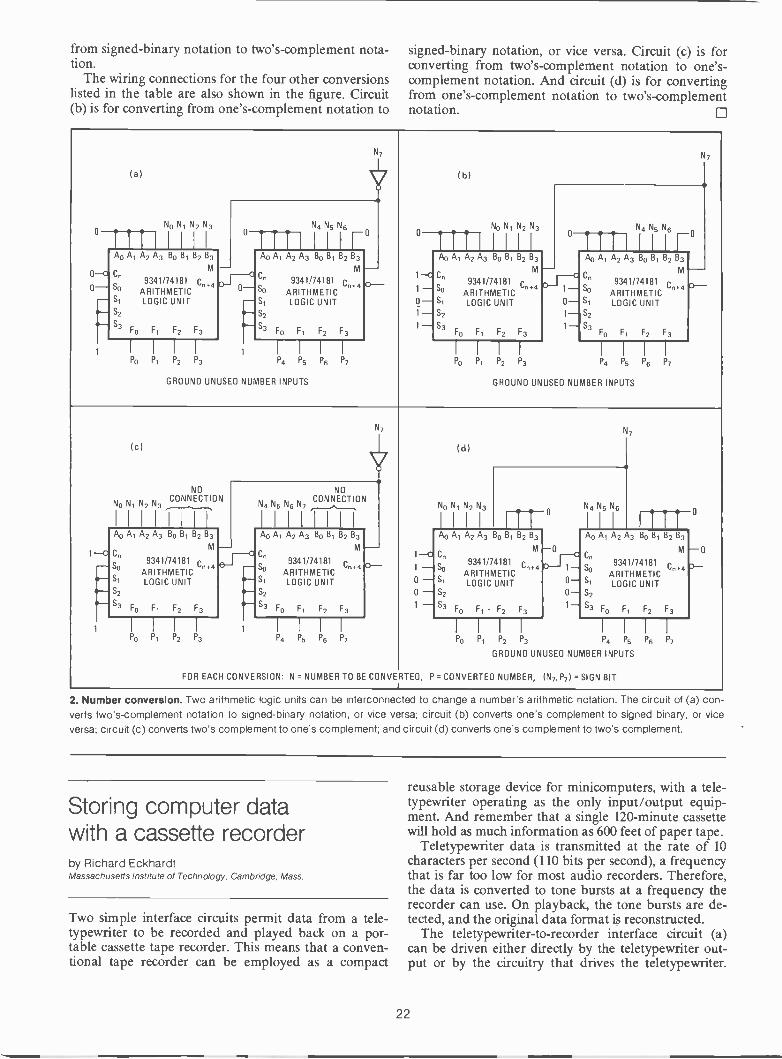
from signed -binary notation to two's -complement nota-tion.
The wiring connections for the four other conversionslisted in the table are also shown in the figure. Circuit(b) is for converting from one's -complement notation to
signed -binary notation, or vice versa. Circuit (c) is forconverting from two's -complement notation to one's-
complement notation. And circuit (d) is for convertingfrom one's -complement notation to two's -complementnotation. El
0
(a)
No Ni N2 N3
1'
0-c0--
Ao Al A2 A3 Bo Bi B2 B3
Cn
So9341/74181 Cn.4
ARITHMETICSI LOGIC UNIT
Sz
S3Fo F, F2 F3
N7
N4 N5 86
0
°.-j 0-c
So
S,
S2
S3
Ao Al A2 A3 Bo B1 B2 B3
9341/74181 Cn.4
ARITHMETICLOGIC UNIT
0
0 F1 F2 F3
PO P1 P2 P3 P4 P5 P6 P7
GROUND UNUSED NUMBER INPUTS
0-
0
(b(
No Ni N2 N3
1-c1-0-1-1-
Cn
So
Si
S2
3
Ao Al A2 A3 Bo Bi 82 B3M
9341/74181 r,na4ARITHMETICLOGIC UNIT
Fo F1 F2 F3
N7
0N4 N5 N6
or -3-
I I I
PO P1 P2 P3
0-1-1-
n 9341/74181 cn,4So ARITHMETICS1 LOGIC UNIT
S2
3Fo F1 F2 F3
Ao Al A2 A3 Bo B1 B2 B3
C M
I I I
P4 P5 P6 P7
GROUND UNUSED NUMBER INPUTS
0-
(c(
NOCONNECTIONNo Ni N2 N3
1 1
Ao Ai A2 A3 Bo B1 B2 B3
1-c- So 9341/74181 cn,4
ARITHMETICS1 LOGIC UNIT
--` S20- S3
Mc
Fo F1 F2 F3
I I 1
PO P1 P2 P3
N7
-14-
14-
Cn
So
Si
S2
S3 F0 F1
NO
N4 N5 N6 N7CONNECTION
11111111Ao Al A2 A3 Bo Bi B2 B3
M
Cn,49341/74181ARITHMETICLOGIC UNIT
F2 F3
0-
I I I
P4 P5 P6 P7
FOR EACH CONVERSION: N = NUMBER TO BE CONVE
No N1 N2 N3
I I I
------
1-0 Cn
1 - So
Ao Al A2 A3 Bo B1 B2 B3
M
0-S10 - G21 - S3
Fo F1 F2 F3
9341/74181 r1,4-4
ARITHMETICLOGIC UNIT
I I I
Cn
So
51
S2
S3 Fo F1
7
I4
N5 N60
Ao Al A2 A3 Bo Bi 82 83
M
9341/74181 r.na-4ARITHMETICLOGIC UNIT
F2 F3
-00-
PO P1 P2 P3 P4 P5 P6 P7
GROUND UNUSED NUMBER INPUTS
RTED, P = CONVERTED NUMBER, IN7, P7) =SIGN BIT
2. Number conversion. Two arithmetic logic units can be interconnected to change a number's arithmetic notation. The circuit of (a) converts two's -complement notation to signed -binary notation, or vice versa; circuit (b) converts one's complement to signed binary, or viceversa; circuit (c) converts two's complement to one's complement; and circuit (d) converts one's complement to two's complement.
Storing computer datawith a cassette recorderby Richard EckhardtMassachusetts Institute of Technology, Cambridge, Mass.
Two simple interface circuits permit data from a tele-typewriter to be recorded and played back on a por-table cassette tape recorder. This means that a conven-tional tape recorder can be employed as a compact
reusable storage device for minicomputers, with a tele-typewriter operating as the only input/output equip-ment. And remember that a single 120 -minute cassettewill hold as much information as 600 feet of paper tape.
Teletypewriter data is transmitted at the rate of 10characters per second (110 bits per second), a frequencythat is far too low for most audio recorders. Therefore,the data is converted to tone bursts at a frequency therecorder can use. On playback, the tone bursts are de-tected, and the original data format is reconstructed.
The teletypewriter -to -recorder interface circuit (a)can be driven either directly by the teletypewriter out-put or by the circuitry that drives the teletypewriter.
22
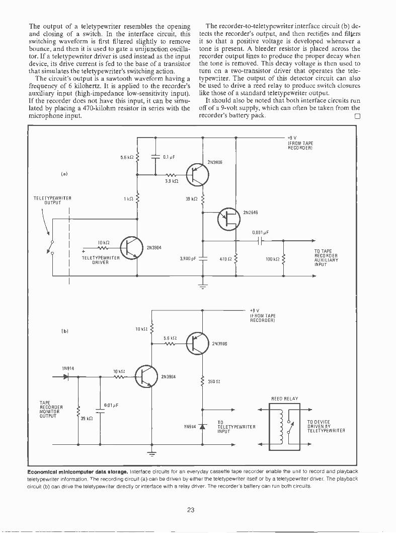
The output of a teletypewriter resembles the openingand closing of a switch. In the interface circuit, thisswitching waveform is first filtered slightly to removebounce, and then it is used to gate a unijunction oscilla-tor. If a teletypewriter driver is used instead as the inputdevice, its drive current is fed to the base of a transistorthat simulates the teletypewriter's switching action.
The circuit's output is a sawtooth waveform having afrequency of 6 kilohertz. It is applied to the recorder'sauxiliary input (high -impedance low -sensitivity input).If the recorder does not have this input, it can be simu-lated by placing a 470-kilohm resistor in series with themicrophone input.
The recorder -to -teletypewriter interface circuit (b) de-tects the recorder's output, and then rectifies and filtersit so that a positive voltage is developed whenever atone is present. A bleeder resistor is placed across therecorder output lines to produce the proper decay whenthe tone is removed. This decay voltage is then used toturn on a two -transistor driver that operates the tele-typewriter. The output of this detector circuit can alsobe used to drive a reed relay to produce switch closureslike those of a standard teletypewriter output.
It should also be noted that both interface circuits runoff of a 9 -volt supply, which can often be taken from therecorder's battery pack.
(a)
TELETYPEWRITEROUTPUT
5.6 1(2 0.1 p F
3.9 kS2
1 kS2. 39 kS2
10 ktl
TELETYPEWRITERDRIVER
2N3904
3,900 pF
2N3906
2N2646
0.001 pF
+9 V(FROM TAPERECORDER)
470 S2 Z 100 kS2
TO TAPERECORDERAUXILIARYINPUT
(b)
1N91410 k2
TAPERECORDERMONITOROUTPUT
39 k,f2
0.01 pF
10 kS2
5.6 kS2
2N3904
2N3906
390 El
+9 V(FROM TAPERECORDER)
REED RELAY
TO O TO DEVICE1N914 TELETYPEWRITER DRIVEN BY
INPUT TELETYPEWRITER
Economical minicomputer data storage. Interface circuits for an everyday cassette tape recorder enable the unit to record and playbackteletypewriter information. The recording circuit (a) can be driven by either the teletypewriter itself or by a teletypewriter driver. The playbackcircuit (b) can drive the teletypewriter directly or interface with a relay driver. The recorder's battery can run both circuits.
23
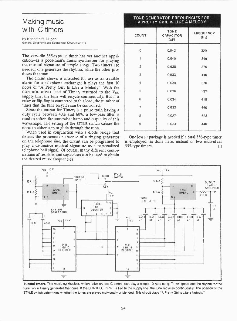
Making musicwith IC timersby Kenneth R. DuganGeneral Telephone and Electronics, Clearwater, Fla.
The versatile 555 -type lc timer has yet another appli-cation-as a poor -man's music synthesizer for playingthe musical signature of simple songs. Two timers areneeded: one generates the rhythm, while the other pro-duces the tones.
The circuit shown is intended for use as an audiblealarm for a telephone exchange; it plays the first 10notes of "A Pretty Girl Is Like a Melody." With theCONTROL INPUT lead of Timers returned to the Vccsupply line, the tune will recycle continuously. But if arelay or flip-flop is connected to this lead, the number oftimes that the tune recycles can be controlled.
Since the output for Time% is a pulse train having aduty cycle between 40% and 60%, a low-pass filter isused to soften the somewhat harsh audio quality of thiswaveshape. The setting of the STYLE switch causes thenotes to either step or glide through the tune.
When used in conjunction with a diode bridge thatdetects the presence or absence of a ringing generatoron the telephone line, the circuit can be programed toplay a distinctive musical signature as a personalizedtelephone bell signal. Of course, many different combi-nations of resistors and capacitors can be used to obtainthe desired music frequencies.
TONE -GENERATOR FREQUENCIES FOR"A PRETTY GIRL IS LIKE A MELODY"
COUNTTONE
CAPACITOR(µF)
FREQUENCY(Hz)
0
1
2
3
4
5
6
7
8
9
0.042
0.040
0.038
0.033
0.038
0.036
0.034
0.033
0.027
0.033
329
349
370
440
370
392
415
440
523
440
One less IC package is needed if a dual 556 -type timeris employed, as done here, instead of two individual555 -type timers.
10 kS.2
15 k2
vcc 5V
1 14
'k 556TIMERZ
6 7
IRHYTHMGENERATOR
CONTROLINPUT
STYLESLUR
SWITCH
Vcc +5 V10µF 22 µF
16
15
8
9
0 13
14
11
10
74411 OF 10 7
DECODER
12
0KEY
Vcc1 +5 V
7490 5 10
DECADE14 2
COUNTER
12 1 9 8 11 6
Vcc
1+"
Vcc
21 k52
42 kS2
TONEGENERATOR
5V
13
12 8
'A 556TIMER2
OUTPUT
10 TO AUDIOAMPLIFIER
9 -MA., --0-10.910 S2
0.042 0.04µF µF
16
15
8
9
74411 OF 10 13
DECODER 14
11
10
12
0.038µF
0.033µF
0.036µF
0.034/IF
0.027µF
0.5µF
Tuneful Union. This music synthesizer, which relies on two IC timers, can play a simple 10 -note song. Timer, generates the rhythm for thetune, while Timer2 generates the tones. If the CONTROL INPUT is tied to the supply line, the tune recycles continuously. The position of theSTYLE switch determines whether the tones are played individually or blended. This circuit plays "A Pretty Girl Is Like a Melody."
24

Schottky diode pair makesan rf detector stableby Roland J. TurnerAEL Communications Corp., Lansdale, Pa.
If broadband rf detection is to be efficient at low signallevels, detection thresholds must be stable-a designgoal achievable with a pair of matched Schottky diodes.The diode -stabilized circuit shown here, for instance,maintains a detection stability of ±0.06 decibel over atemperature range of -20°C to + 90°C for an rf drivelevel that is a 10th of that of a conventional detector.
With such a circuit, the amount of if circuitry re-quired can be much reduced because accurate stabilizeddetection thresholds can be set for low rf drive levels.Also, the circuit's temperature stability and detection ef-ficiency permit the realization of a sensitive receiver-one that can have a high video gain as well as a low rfgain.
Normally, it is hard to achieve high detection effi-ciency at a low rf drive level while keeping detection ef-ficiency constant over a wide temperature range. This isbecause of the nature of the forward blocking voltage of
a diode. For example, at room temperature, a silicondiode has a forward voltage of about 500 millivolts anda temperature coefficient of 2 my/°C, so that the for-ward voltage will vary considerably-from 370 my at90°C to 590 my at -20°C.
The rf drive level needed to start the detection actionmust exceed the diode's forward blocking voltage sothat load current may flow. However, since the forwardvoltage changes by 220 my from -20°C to + 90°C, the rfdrive level required must vary accordingly to maintaindetection action. The inherent detection efficiency,therefore, is low and strongly dependent on tempera-ture, limiting the maximum video gain that may followthe detector.
The rf detector depicted here, though, solves theseproblems. The two Schottky diodes, D1 and D2, arematched to within 5 my from 0.1 to 0.5 milliampere andare connected in a half -wave rf detector configuration.The dc bias developed across diode D2 and resistor R1serves as an arming bias for the detector diode, Di, es-tablishing temperature tracking between the two diodes.
The voltage drop across resistor R1 establishes a re-verse offset bias on diode D1, in this way setting aknown rf threshold that the rf drive level must exceedbefore detection action takes place. And the voltagedrop across diode D2 acts as a temperature -dependentforward arming bias on diode D1. The level of this arm -
INPUT
22 'AFT
390 pF
7552
1852
HP5082-2023
01
I17 TURNSCF1O1 1,500 pF -MATERIAL 01 (CERAMIC)
0.02 2.2 k2HP5082-2023
pF
1.1 kit(%W)
8.852 33052
1% METAL FILM
0.02 pF
2N2907A
1N914
2.2 k2 220 kS2
J
560 n
1%
METALFILM
24 V
1N823
3.9 kE2
2 7
MOTOROLAMC1741G
3 4
OUTPUT
Temperature stabilized. High -efficiency rf detector operates at low input drive levels over a wide temperature range. Matched Schottkydiodes (D1 and D2) and a fixed rf threshold bias (via resistor R1) permit the circuit to hold voltage detection stability to ±0.06 dB from-20°C to+ 90°C for a 55 -mV input. Sensitivity to supply -voltage changes can be minimized by adding colored network (and omitting FI1).
25

ing bias tracks the forward blocking voltage of diode D1as the temperature changes.
Because of this temperature -compensating armingbias, it is possible to realize constant detection efficiencyover a wide temperature range, in addition to a constantrf threshold detection level. For a constant rf input of55 my, the detection voltage developed by the circuitvaries only 1.8 my between -20°C and +90°C. Rf peakvoltages as large as 80 my can be detected quite ef-ficiently.
The operational amplifier at the output of the circuitsenses the detection voltage and translates it to a 12 -volt
level. This output voltage varies only 2.1% from -20°Cto +90°C for a constant rf input drive. Here, the opamp's gain is 40 dB, a figure that can be safely increasedto 50 dB without adversely affecting the output stabilityof the circuit.
The circuit's performance will be further enhanced ifthe detector is made insensitive to variations in supplyvoltage. This can be done by adding a current source(shown in color in the diagram). The current sourcekeeps the rf threshold voltage constant, despite supplyvariations of ±0.5 v. In connecting this source, resistorR1 must be omitted.
Crowbar protection circuitsenses load voltage directlyby Thomas E. SkopalAcopian Corp., Easton, Pa.
The triggering point of the overvoltage-protection crow-bar circuit for a power supply can be decreased withoutincreasing the circuit's sensitivity to transients. The trickis to have the crowbar circuit sense the voltage acrossthe load, rather than the output voltage of the powersupply, as is usually done.
To provide maximum protection, a crowbar circuit isgenerally set reasonably close to the operating voltagerequired by the load. Typically, a compromise setting ofabout 15% above the load's operating voltage is chosen,because commonly encountered transients may causespurious crowbar triggering and interfere with normalsystem operation if a tighter differential is used.
However, when voltage drops in the supply's output
wiring exceed 2% or 3% of the output voltage-a com-mon occurrence with low -voltage, high -current logicsupplies-the system designer is faced with a dilemma.If he compensates for these drops with an increase inpower -supply output voltage, the differential will be re-duced and the crowbar's sensitivity to transients in-creased. And if crowbar setting is increased to maintainthe same differential, load protection is degraded.
This conflict can be resolved by using the four -termi-nal crowbar circuit shown in the figure. It senses thevoltage across the load, much as a supply's remote -sen-sing connections may be used to automatically compen-sate for voltage drops caused by long wires.
The crowbar's triggering point is a function of thevoltage seen by the load, as opposed to the output volt-age of the supply, and it is unaffected by the amplitudeof the wiring voltage drops. Since the sensing connec-tions of the crowbar share the sense lines of the supply'sregulator, no additional system wiring is required.
The diode in the circuit provides temperature com-pensation for the transistor. The component valuesgiven are appropriate for power supplies having outputsof 4 to 10 volts and of up to 20 amperes.
POWER SUPPLY
(+1 OUTPUT
(+1 SENSE
(-1 SENSE
(-) OUTPUT
2N681
56 Si
2N2904
100 Si
1N914
TRIGGERADJUST500 St
1 kS2
LOAD
Better protection. Crowbar circuit protects a power supply from overvoltages by sensing the voltage across the load, instead of the supply'soutput voltage, which is the usual approach. This means that overvoltage sensing will not be affected by wiring voltage drops, nor will therebe an increased sensitivity to voltage transients. The components shown here are for a power supply of 4 to 10 volts at up to 20amperes.
26
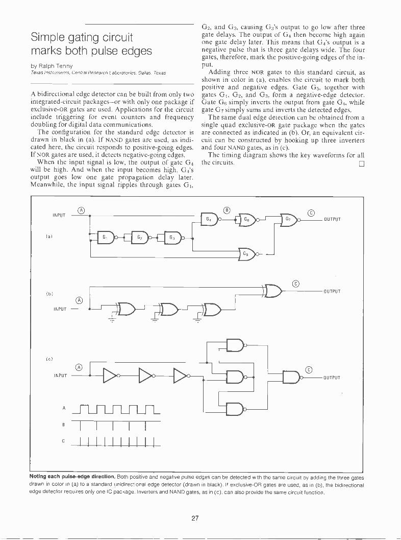
Simple gating circuitmarks both pulse edgesby Ralph TennyTexas Instruments. Central Research Laboratories, Dallas, Texas
A bidirectional edge detector can be built from only twointegrated -circuit packages-or with only one package ifexclusive -OR gates are used. Applications for the circuitinclude triggering for event counters and frequencydoubling for digital data communications.
The configuration for the standard edge detector isdrawn in black in (a). If NAND gates are used, as indi-cated here, the circuit responds to positive -going edges.If NOR gates are used, it detects negative -going edges.
When the input signal is low, the output of gate G4will be high. And when the input becomes high, G4'soutput goes low one gate propagation delay later.Meanwhile, the input signal ripples through gates G1,
G2, and G3, causing G3's output to go low after threegate delays. The output of G4 then become high againone gate delay later. This means that G4's output is anegative pulse that is three gate delays wide. The fourgates, therefore, mark the positive -going edges of the in-put.
Adding three NOR gates to this standard circuit, asshown in color in (a), enables the circuit to mark bothpositive and negative edges. Gate G5, together withgates G1, G2, and G3, form a negative -edge detector.Gate G6 simply inverts the output from gate G4, whilegate G7 simply sums and inverts the detected edges.
The same dual edge detection can be obtained from asingle quad exclusive -OR gate package when the gatesare connected as indicated in (b). Or, an equivalent cir-cuit can be constructed by hooking up three invertersand four NAND gates, as in (c).
The timing diagram shows the key waveforms for allthe circuits.
Noting each pulse -edge direction. Both positive and negative pulse edges can be detected with the same circuit by adding the three gatesdrawn in color in (a) to a standard unidirectional edge detector (drawn in black). If exclusive -OR gates are used, as in (b), the bidirectionaledge detector requires only one IC package. Inverters and NAND gates, as in (c), can also provide the same circuit function.
27
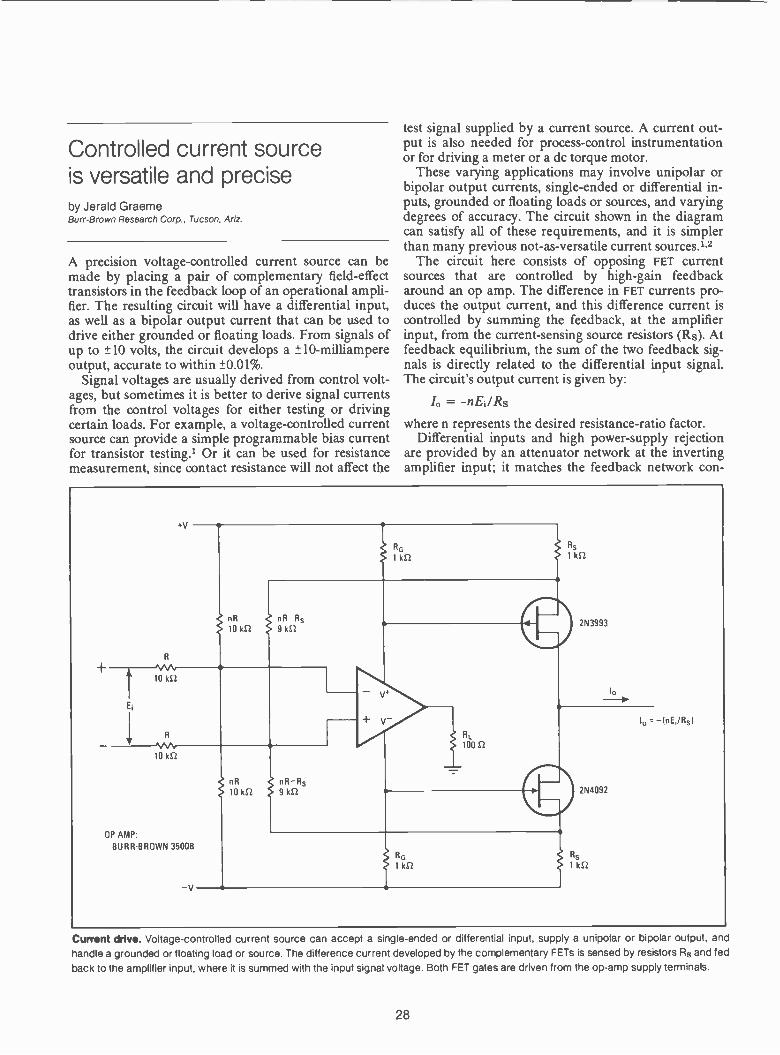
Controlled current sourceis versatile and preciseby Jerald GraemeBurr -Brown Research Corp., Tucson, Ariz.
A precision voltage -controlled current source can bemade by placing a pair of complementary field-effecttransistors in the feedback loop of an operational ampli-fier. The resulting circuit will have a differential input,as well as a bipolar output current that can be used todrive either grounded or floating loads. From signals ofup to ±10 volts, the circuit develops a ±-10-milliampereoutput, accurate to within ±0.01%.
Signal voltages are usually derived from control volt-ages, but sometimes it is better to derive signal currentsfrom the control voltages for either testing or drivingcertain loads. For example, a voltage -controlled currentsource can provide a simple programmable bias currentfor transistor testing.1 Or it can be used for resistancemeasurement, since contact resistance will not affect the
test signal supplied by a current source. A current out-put is also needed for process -control instrumentationor for driving a meter or a dc torque motor.
These varying applications may involve unipolar orbipolar output currents, single -ended or differential in-puts, grounded or floating loads or sources, and varyingdegrees of accuracy. The circuit shown in the diagramcan satisfy all of these requirements, and it is simplerthan many previous not -as -versatile current sources.1,2
The circuit here consists of opposing FET currentsources that are controlled by high -gain feedbackaround an op amp. The difference in FET currents pro-duces the output current, and this difference current iscontrolled by summing the feedback, at the amplifierinput, from the current -sensing source resistors (Rs). Atfeedback equilibrium, the sum of the two feedback sig-nals is directly related to the differential input signal.The circuit's output current is given by:
to = -nE,/ Rs
where n represents the desired resistance -ratio factor.Differential inputs and high power -supply rejection
are provided by an attenuator network at the invertingamplifier input; it matches the feedback network con -
Current drive. Voltage -controlled current source can accept a single -ended or differential input, supply a unipolar or bipolar output, andhandle a grounded or floating load or source. The difference current developed by the complementary FETs is sensed by resistors Rs and fedback to the amplifier input, where it is summed with the input signal voltage. Both FET gates are driven from the op -amp supply terminals.
28

nected to the other amplifier input. This is analogous tothe matched input and feedback networks connected toan op amp to form the common difference amplifier.2
To simplify biasing and improve large -signal band-width, the gates of both FETS are driven from the op -amp supply terminals, rather than from the op -ampoutput terminal. Quiescent biasing for the FETs is ob-tained from the quiescent current drains of the op amp,and no level -shifting bias must be set up from the am-plifer to the FETs.
Large -signal bandwidth is also improved by the re-duced output swing required from the amplifier. Only a1 -volt swing is needed across amplifier load resistor RLto obtain the rated output current, which is drawnthrough the supply terminals for maximum drive to theFETS.
Additionally, the lower amplifier output swing is notas greatly bandwidth -limited by the amplifier slewing-rate limit, as it is in other designs. Optimum bandwidthis achieved by making resistor RL small enough to limitoutput swing without excessively lowering amplifiergain. Large -signal bandwidth is then limited by the am-plifier's maximum common -mode swing rate.
The circuit's output current is controlled by the inputvoltage to within the accuracies of the resistors selectedand within the gain -bandwidth and power -supply -rejec-
tion limitations of the op amp used. Most accuracy limi-tations caused by the FETS are overcome by the feed-back, except for the small contributions from gate -drainleakage currents.
Output current is limited to the IDss level of the FETsbut can be boosted by using the transconductance mul-tiplying technique sometimes employed for commonFET controlled current sources.' Output impedance ismultiplied, through the feedback, from that of the FETS
to the practical limit imposed by stray and parasitic ef-fects-it is around 1012 ohms shunted by 10 picofarads.
By virtue of the circuit's differential inputs, common -
mode signals are eliminated by a common -mode rejec-tion that is adjustable to over 90 decibels. The primarycommon -mode -rejection limitations are the accuraciesof the resistor ratios and the resistor matches, except forthe noncritical match between the FET gate resistors(RG)
The common -mode rejection can be adjusted by trim-ming the input resistors. Prior to this adjustment, anydesired nulling of dc offset voltage should be performedby trimming the resistors denoted as nR.
REFERENCES1 J. Graeme, "Applications of Operational Amplifiers-Third Generation Techniques,"McGraw-Hill, New York. 1973.2. G Tobey, J. Graeme, and L. Huelsman, "Operational Amplifiers-Design and Appli-cations," McGraw-Hill, New York, 1971.
Single bipolar transistorinverts pulses on commandBy Dale HilemanSphygmetrics Inc., Woodland Hills, Calif.
An ordinary bipolar transistor can be made to functionas a command inverter-that is, it will pass a pulse sig-nal without modifying the pulse, but it can invert the
signal upon command. The command is a simple rever-sal of the polarity of the supply voltage.
To do this usually requires several gates, involvingperhaps dozens of parts and interconnections. The com-mand inverter shown here, however, requires only threeparts: a single bipolar transistor and two ordinary re-sistors.
The key to this circuit's operation is that the role of atransistor's emitter and collector can be interchanged ifthe supply polarity is reversed. When the polarity of theinvert control signal is normal, the transistor operates asan emitter -follower, so that the polarity of the output
Command Invader. With normal supply polarity, this bipolar transistor operates as an emitter -follower, passing the input pulse train to theoutput without modifying it. But when the supply polarity is reversed, the transistor's emitter acts as its collector, and the transistor's collectoracts as its emitter. Now the polarity of the input pulse train will be inverted at the transistor's output.
29

pulse train is the same as the polarity of the input pulsetrain.
The invert command reverses the polarity of the sup-ply voltage, making the transistor's collector act as anemitter and its emitter act as a collector. Now the circuitbecomes an inverting amplifier, with resistor R1 servingas the collector load resistor. Under this condition, re-sistor R2 simply limits the transistor base current to asafe value.
Any general-purpose npn or pnp bipolar transistormay be used in the circuit, and the precision of neitherresistor Ri nor resistor R2 is critical. This command in-verter will work with virtually any value of supply volt-age and any input pulse level that the transistor will tol-erate. El
Norton quad amplifier can bea low-cost function generatorby P. VicekOrbit Controls Ltd.,Cheltenham, Gloucester, England
A versatile function generator that minimizes hardwareas well as cost can be built with one of the newly intro-duced Norton quad amplifiers [Electronics, Dec. 6,1973, pp. 116-120]. The price of the complete generatoris less than $3, and the entire unit can fit on a circuitboard as small as a 11/2 -inch square.
Only a single Norton amplifier is needed to obtain a
(a)
R) 39 kS2
1 MO+V -We -6-
330 kit
SYMMETRYADJUST
220 at
(b)
f\f\..
sine -wave generator (a). When resistor R1 and capacitorCI are omitted from this circuit, the resulting configura-tion is the standard one for a Norton -amplifier square -wave generator, with the timing current passing throughcapacitor C2.
The addition of integrating capacitor Ci to thissquare -wave generator produces a resonably accuratesine wave at the output. Resistor 'Ri, which helps tomatch the circuit's time constants, can be used to adjustthe output sine wave for minimum distortion.
A similar circuit can be used to add a sine -wave out-put to the conventional hookup for a square-wave/triangular-wave generator built with two Nortonamplifiers. As shown in (b), the triangular output acts asthe input for the sine -shaper amplifier.
For the component values given here, the circuit's op-erating frequency is around 700 hertz. Resistor R1 is theadjustment for minimum sine -wave distortion, and re-sistor R2 is the adjustment for the symmetry of thesquare and triangular waves.
The fourth amplifier in the Norton quad package canbe connected as an output buffer for- all three outputwaveforms. 1:1
Economical approach. Norton quad amplifier, which is one of thenewer ICs, reduces the circuitry and the cost of waveform gener-ation. If a single amplifier is used, as in (a), a sine wave can be gen-erated, with provision (through resistor R1) for minimizing distortion.With three amplifiers, as in (b), triangular, square, and sine wave-forms can be obtained, and the fourth amplifier can act as a buffer.
0.001uF
100
%LM3900
%LM3900
1 MS2 100 k.O.
+V
SINEADJUST
Ri 22 kS2
22 kg/ 55 pF
3.3 ma
_r- 0.01µF
_L
0%LM3900
10 MU 10 Mit
30
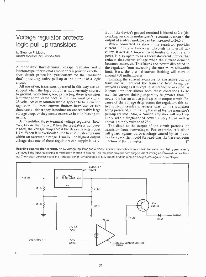
Voltage regulator protectslogic pull-up transistorsby Stephen F. MooreResdel Engineering Corp., Arcadia, Calif
A monolithic three -terminal voltage regulator and aNorton -type operational amplifier can provide excellentshort-circuit protection-particularly for the transistorthat's providing active pull-up at the output of a logiccircuit.
All too often, transistors operated in this way are de-stroyed when the logic output is inadvertently shortedto ground. Sometimes, too, protecting these transistorsis further complicated because the logic must be run at28 volts. An easy solution would appear to be a currentregulator. But most current limiters have one of twodrawbacks-either they introduce an unacceptably largevoltage drop, or they create excessive heat in biasing re-sistors.
A monolithic three -terminal voltage regulator, how-ever, has neither defect. When the regulator is not over-loaded, the voltage drop across the device is only about1.5 v. When it is overloaded, the heat it creates remainswithin an acceptable range. Usually, the highest outputvoltage that one of these regulators can supply is 24 v.
But, if the device's ground terminal is biased at 2 v (de-pending on the manufacturer's recommendations), theoutput of a 24-v regulator can be increased to 26.5 v.
When connected as shown, the regulator providescurrent limiting in two ways. Through its internal cir-cuitry, it acts as a surge -current limiter of about 2 am-peres. It also operates as a thermal -current limiter thatreduces that output voltage when the current demandbecomes excessive. This keeps the power dissipated inthe regulator from exceeding the maximum allowablelimit. Here, the thermal -current limiting will start ataround 400 milliamperes.
Limiting the current available for the active -pull-uptransistor will prevent the transistor from being de-stroyed as long as it is kept in saturation or in cutoff. ANorton amplifier allows both these conditions to bemet-its current -sinking capability is greater than 30mA, and it has an active pull-up in its output circuit. Be-cause of the voltage drop across the regulator, this ac-tive pull-up creates a reverse bias on the transistorbeing protected, eliminating the need for the transistor'spull-up resistor. Also, a Norton amplifier will work re-liably with a single -ended power supply at, as well asabove, a supply voltage of 28 v.
The diode at the output of the circuit protects thetransistor from overvoltages. For example, this diodewill guard against an overvoltage caused by an induc-tive kickback that could forward -bias the base -collectorjunction of the transistor.
Guarding against short circuits. An IC voltage regulator and a Norton amplifier keep this active -pull-up transistor from being permanentlydamaged if the input logic signal is mistakenly shorted to ground. The regulator provides both surge -current limiting and thermal -current limit-ing. The Norton amplifier keeps the transistor either fully saturated or fully cut off, and the output diode protects against overvoltages.
+28 Vdc
12 kS2
12 kS2.
LOGIC INPUT
VOLTAGEIN REGULATOR OUT
GND
FAIRCHILD78M24
270 k/2
5.1 kS2
390 S2
270 1(12
+28 Vdc1.5 kfl
NATIONAL SEMICONDUCTOR% LM2900
RCA2N5783
OUTPUT
11\1649
31
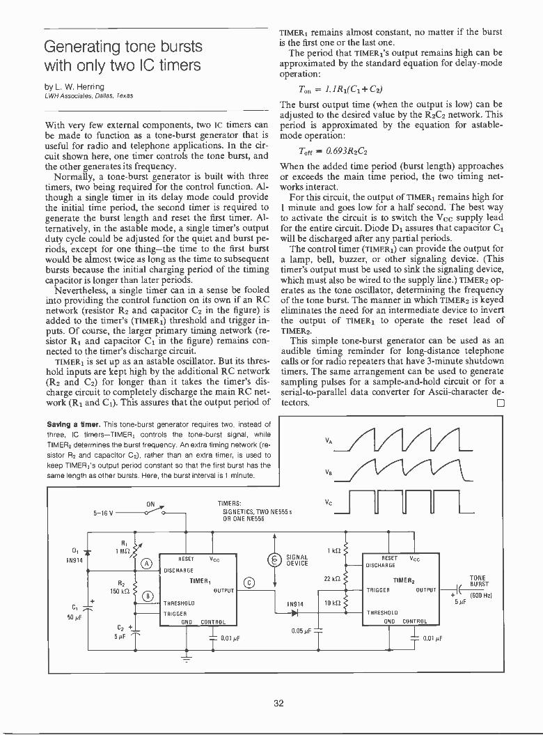
Generating tone burstswith only two IC timersby L. W. HerringLWH Associates, Dallas, Texas
With very few external components, two IC timers canbe made to function as a tone -burst generator that isuseful for radio and telephone applications. In the cir-cuit shown here, one timer controls the tone burst, andthe other generates its frequency.
Normally, a tone -burst generator is built with threetimers, two being required for the control function. Al-though a single timer in its delay mode could providethe initial time period, the second timer is required togenerate the burst length and reset the first timer. Al-ternatively, in the astable mode, a single timer's outputduty cycle could be adjusted for the quiet and burst pe-riods, except for one thing-the time to the first burstwould be almost twice as long as the time to subsequentbursts because the initial charging period of the timingcapacitor is longer than later periods.
Nevertheless, a single timer can in a sense be fooledinto providing the control function on its own if an RCnetwork (resistor R2 and capacitor C2 in the figure) isadded to the timer's (TIMER1) threshold and trigger in-puts. Of course, the larger primary timing network (re-sistor R1 and capacitor C1 in the figure) remains con-nected to the timer's discharge circuit.
TIMERi is set up as an astable oscillator. But its thres-hold inputs are kept high by the additional RC network(R2 and C2) for longer than it takes the timer's dis-charge circuit to completely discharge the main RC net-work (R1 and Cf.). This assures that the output period of
Saving a timer. This tone -burst generator requires two, instead ofthree, IC timers-TIMER' controls the tone -burst signal, while
TIMER2 determines the burst frequency. An extra timing network (re-sistor R2 and capacitor C2), rather than an extra timer, is used tokeep TIMER''s output period constant so that the first burst has thesame length as other bursts. Here, the burst interval is 1 minute.
TIMERi remains almost constant, no matter if the burstis the first one or the last one.
The period that TIMERi's output remains high can beapproximated by the standard equation for delay -modeoperation:
To. = 1.1R1(C1+ C2)
The burst output time (when the output is low) can beadjusted to the desired value by the R2C2 network. Thisperiod is approximated by the equation for astable -mode operation:
Toff = 0.693R2C2
When the added time period (burst length) approachesor exceeds the main time period, the two timing net-works interact.
For this circuit, the output of TIMER]. remains high for1 minute and goes low for a half second. The best wayto activate the circuit is to switch the Vcc supply leadfor the entire circuit. Diode D1 assures that capacitor C1will be discharged after any partial periods.
The control timer (TIMER1) can provide the output fora lamp, bell, buzzer, or other signaling device. (Thistimer's output must be used to sink the signaling device,which must also be wired to the supply line.) TIMER2 op-erates as the tone oscillator, determining the frequencyof the tone burst. The manner in which TIMER2 is keyedeliminates the need for an intermediate device to invertthe output of TIMERi to operate the reset lead ofTIMER2.
This simple tone -burst generator can be used as anaudible timing reminder for long-distance telephonecalls or for radio repeaters that have 3 -minute shutdowntimers. The same arrangement can be used to generatesampling pulses for a sample -and -hold circuit or for aserial -to -parallel data converter for Ascii-character de-tectors.
vA_77.77_vB
1N914
ON TIMERS:
SIGNETICS, TWO NE555 sOR ONE NE556
vc
5-16 V
Ri
1 MS2SIGNALDEVICE
1 kS2
RESET Vcc
DISCHARGE
RESET VccDISCHARGE
R2TIMERi 22 kft TIMER2 TONE
BURST
150 1(11 OUTPUT TRIGGER OUTPUT
+ (600 Hz)- THRESHOLD 1N914 10 5µF
50TRIGGER THRESHOLD
GND CONTROL GNO CONTROL
C2 0.05 /IF -5µF 0.01 µF 0.01 µF
32
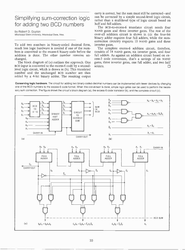
Simplifying sum -correction logicfor adding two BCD numbersby Robert D. GuytonMississippi State University, Mississippi State, Miss.
To add two numbers in binary-coded decimal form,much less logic hardware is needed if one of the num-bers is converted to the excess -6 binary code before theaddition is done. The other number remains un-changed.
The block diagram of (a) outlines the approach. OneBCD input is converted to the excess -6 code by a second -level logic circuit, which is drawn in (b). This translatednumber and the unchanged BCD number are thenadded by a 4 -bit binary adder. The resulting output
carry is correct, but the sum must still be corrected-andcan be corrected by a simple second -level logic circuit,rather than a multilevel type of logic circuit based onhalf and full adders.
The BCD -to -excess -6 translator circuit needs fourNAND gates and three inverter gates. The rest of theover-all addition circuit is shown in (c): the four -bitbinary adder requires four full adders, while the sum -
correction circuitry requires 10 NAND gates and threeinverter gates.
The complete excess -6 addition circuit, therefore,consists of 14 NAND gates, six inverter gates, and fourfull adders. As against an addition circuit based on ex-cess -3 code conversion, that's a savings of six NANDgates, three inverter gates, one full adder, and two halfadders. 0
Conserving logic hardware. The circuit for adding two binary -coded -decimal numbers can be implemented with fewer devices by changingone of the BCD numbers to the excess -6 code format. When this conversion is done, simple logic gates can be used to perform the neces-sary sum correction. The figure shows the circuit's block diagram (a), the excess -6 code translator (b), and the complete circuit (c).
B8
B8 -11.X8 S8 B4
B4 -P. BCD X S4 132SUM
B2-111.-*Ag
TO
X - 6X2
BINARY4 -BIT
ADDER
S2
Si CIRCUITTO
CORRECT
SUM
IN 4
XI -0"BCD
82
A4
4
A2
2
a. 82A,
CARRY -INB,
CARRY -OUT(a) (b)
co
Ag Xg
11FULL
ADDER
CARRY -OUT
A4 X4
FULLADDER
4
A2 X2
Xg = Bg + B4 + B2
X4 = B4 B2 + T3462
X2 = B2
--
FULLADDER
A, X,
1 1
CARRY -IN
FULLADDER
(c) s8c. + s8S4s2 CoS4 + S254 +ZoS2S4 cos2 + cos2
- BCD SUM
33
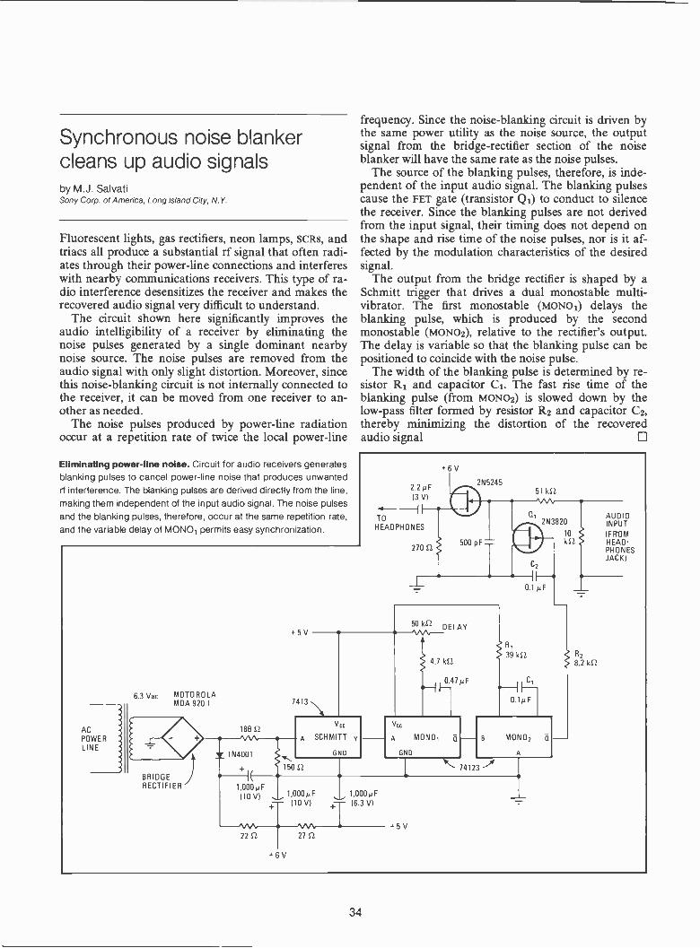
Synchronous noise blankercleans up audio signalsby M.J. SalvatiSony Corp. of America, Long Island City, N.Y.
Fluorescent lights, gas rectifiers, neon lamps, SCRs, andtriacs all produce a substantial rf signal that often radi-ates through their power -line connections and interfereswith nearby communications receivers. This type of ra-dio interference desensitizes the receiver and makes therecovered audio signal very difficult to understand.
The circuit shown here significantly improves theaudio intelligibility of a receiver by eliminating thenoise pulses generated by a single dominant nearbynoise source. The noise pulses are removed from theaudio signal with only slight distortion. Moreover, sincethis noise -blanking circuit is not internally connected tothe receiver, it can be moved from one receiver to an-other as needed.
The noise pulses produced by power -line radiationoccur at a repetition rate of twice the local power -line
Eliminating power -line noise. Circuit for audio receivers generatesblanking pulses to cancel power -line noise that produces unwantedrf interference. The blanking pulses are derived directly from the line,making them independent of the input audio signal. The noise pulsesand the blanking pulses, therefore, occur at the same repetition rate,and the variable delay of MONO, permits easy synchronization.
frequency. Since the noise -blanking circuit is driven bythe same power utility as the noise source, the outputsignal from the bridge -rectifier section of the noiseblanker will have the same rate as the noise pulses.
The source of the blanking pulses, therefore, is inde-pendent of the input audio signal. The blanking pulsescause the FET gate (transistor Qi) to conduct to silencethe receiver. Since the blanking pulses are not derivedfrom the input signal, their timing does not depend onthe shape and rise time of the noise pulses, nor is it af-fected by the modulation characteristics of the desiredsignal.
The output from the bridge rectifier is shaped by aSchmitt trigger that drives a dual monostable multi -vibrator. The first monostable (moNoi) delays theblanking pulse, which is produced by the secondmonostable (moNc,2), relative to the rectifier's output.The delay is variable so that the blanking pulse can bepositioned to coincide with the noise pulse.
The width of the blanking pulse is determined by re-sistor R1 and capacitor C1. The fast rise time of theblanking pulse (from MONO2) is slowed down by thelow-pass filter formed by resistor R2 and capacitor C2,thereby minimizing the distortion of the recoveredaudio signal
ACPOWERLINE
6.3 Vac MOTOROLAMDA 920-1
BRIDGERECTIFIER
+ 5 V
7413
+ 6 V
2.2 pF13 VI
"4-I ITOHEADPHONES
18852
1N4001
150 52
1,000µF(10 V)
vcc
SCHMITT y
GND
270 62500
2N5245
511.-- 0 kil DELAYA,-
4.7 k6
EL47pF
vcc
A MONO,
ONO
51 kS7.
a,2N3820
10
kS2
C2
H.0 1 pF
39 k62
0.1µF
MONO2
74123 -2V
1,000pF(10 VI
2252
+ 6 V
+- 16.3 VI
2752+ 5 V
AUDIOINPUT
(FROMHEAD-PHONESJACK)
8.2RZ kS2
34

Variable voltage source hasindependently adjustable TCby Nathan 0. SokalDesign Automation Inc., Lexington, Mass.
A reference voltage source, which is built around a suit-ably stable general-purpose operational amplifier,offers an adjustable output -voltage magnitude, as wellas an adjustable output -voltage temperature coefficient.Both the voltage magnitude and the temperature coeffi-cient may be varied independently of each other.
The output voltage can be positive or negative, and itis continuously variable from 0.7 to 13 v. The tempera-ture coefficient is also continuously variable, from-0.3%/°C to +0.3%/°C. For the circuit shown in thefigure, the output voltage is positive. To obtain a nega-tive voltage, the polarities of all the diodes and the sup-ply (except to the op amp) are simply reversed.
The temperature coefficients of the zener-diode volt-age, the resistance values, the op -amp input offset volt-age, the op -amp input bias and offset currents, and thepower -supply voltage need not all be zero. Rather, theirvalues as functions of temperature must be stable withtime and retrace well with temperature cycling. This isalso true of the V -I characteristics of diodes D1 and D2.Moreover, these two diodes do not have to be matched.
If a narrower range of output voltage is adequate,part of resistance Ri should be a stable fixed resistor.Likewise, if a narrower temperature -coefficient range issatisfactory, part of resistance R2 should be a stablefixed resistor. Resistances R1, R2, and R3 should bemulti -turn potentiometers if both wide -range adjust-ment and high resolution are desired. Or they should becombinations of potentiometers and fixed resistors if anarrow adjustment range will do. Or they should be
only fixed resistors when the desired output voltage andtemperature coefficient need not be adjusted.
The fixed resistors used in this circuit should be filmor wire -wound types for good long-term stability. A ref-erence -type zener diode, such as the 1N4894, will im-prove voltage stability still further. All the resistors andsemiconductor devices should be thermally coupled toeach other for a good transient response to changes inambient temperature.
A simple procedure can be followed to adjust the cir-cuit to desired operating conditions. First, set poten-tiometers RI and R2 approximately at their mid -rangepositions. Then adjust potentiometer R3 until the volt-age across R2 is zero at the reference temperature. Thisis the temperature at which it must be possible to adjustthe temperature coefficient without changing the outputvoltage. Next, position potentiometer R1 to give the de-sired output voltage at the reference temperature.
The last step is to adjust potentiometer R2 for the de-sired temperature coefficient. This adjustment, whichshould not affect the output voltage at the referencetemperature, can be made by heating or cooling the en-tire circuit to some temperature other than the referencetemperature and then adjusting R2 to obtain the desiredoutput voltage at that temperature.
As a precaution, the circuit's output voltage should bechecked for changing temperature. If it is not within thedesired tolerance, repeat all the adjustment steps butthe first one. Usually no such repetition will be needed.
MOre output current can be obtained from this refer-ence voltage source by adding an npn power transistor,wired as an emitter -follower, at the circuit's output. Theoutput from the op amp goes to this transistor's base,and resistor R1 is then connected to the transistor'semitter, which becomes the circuit output. If the outputvoltage is negative, a pnp emitter -follower should beused. Without an emitter -follower, the output currentcan be as large as 10 milliamperes for most general-pur-pose op amps.
Stable voltage source. The output voltage of this reference voltage source can be adjusted from 0.7 to 13 volts. And the circuit's output-voltage temperature coefficient is also adjustable, from -0.3%/°C to + 0.3% /°C. These two adjustments are independent of each other. Po-tentiometer R1 sets the output voltage, potentiometer R2, the temperature coefficient, and potentiometer R3, the reference temperature.
680
4' 1N753
330
1N4152
1
BALANCE
R3
500 E2
1.0 kE2
TEMPCOADJUST R2
VNA10 kE2
02
1N4152
330 E2
0.1 pF
1.2 1(2
VOLTAGEADJUST
Ri
pA74
0.1 pF
+ 15 V
11
NF
-15 V =.
25 l(S-2
OUTPUT
35

Switched frequency doublerprovides multiple outputsby Michael F. BlackTexas Instruments, Systems Analysis Section, Dallas, Texas
Frequency doublers that operate in the vhf/uhf rangetypically consist of complicated arrangements of satu-rated amplifiers, tuned circuits, and harmonic -suppres-sion traps. With these circuits, a constant input imped-ance is usually difficult to sustain with changingtemperature. Also, if the doubler must be switched, it isdifficult to maintain circuit simplicity and high isolationratios.
The switched frequency doubler shown here, how-ever, provides high harmonic rejection, as well as con-stant input impedance, and it requires a minimum ofadjustment. The circuit, which consists of a double -bal-anced mixer followed by a linear amplifier, accepts a50 -megahertz input of 5 dBm. In addition, it has provi-sion for fast on/off switching and multiple 100 -MHz out-puts to 50 -ohm loads.
The input power is split by the two-way power divi-der, HY I, and applied to the RF and LO ports of themixer, M I. The mixer output, of course, is made up ofseveral frequencies: twice the input frequency, the inputfrequency itself, the difference frequency (between theinput and the local oscillator), and harmonics.
The difference frequency, which is dc, is shorted bythe rf choke (Li), and the input -frequency component isattenuated by the LO/i-f and rf/i-f isolation of themixer. Transistor Qi is tuned to the doubled frequency,and the high -Q circuit in its collector loop further atten-uates the unwanted frequencies to about 50 -dB down.Through inductor L2, the matching structure of this col-lector loop provides the only circuit adjustment.
Only three 50 -ohm outputs are shown here, but more
can be added. For each output, two capacitors (Ci andC2) transform the 50 -ohm load up to a resistance valuethat output transistor Qi can drive satisfactorily. The re-actance of inductor L2 then tunes out the capacitance topresent a high -value real load to Qi's collector at thedoubled frequency.
The value of L2's reactance is:
XL2 =WRP/C9where Rp is the load resistance that transistor Qi sees,and Q is the circuit's figure of merit. The reactances ofthe transformation capacitors, C1 and C2, are also de-pendent on Rp and Q. They can be expressed as:
Xc2= [Rp/(1 +Q2)][Q - [(50/Rp)(1 +Q2) -1j1/2]= 50/[(50/ Rp)(1 +Q2) -1]1/2
Circuit Q is selected according to the harmonic rejec-tion required. The higher the value of Q is, the higherthe harmonic rejection will be, but the more difficultsome component values may become to obtain. For thecircuit given here:
Q = 6Rp = 1.5 kilohmsXL2 = 83 ohms at 100 MHz = 0.13 microhenryXci = 222 ohms at 100 MHz = 6 picofarads
and:Xc2 = 104 ohms at 100 MHz = 15 pF
Each output of the circuit supplies a power level of+3 dBm at a frequency of 100 MHz.
Transistor Q2 is a nonsaturating switch that is com-patible with a TTL open -collector input. Together withits associated circuitry, transistor Q2 switches transistorQi, providing the mutiple gated outputs. Switchingtimes of well under 1 microsecond can be realized whenan appropriate value is chosen for capacitor C3. The cir-cuit's on/off isolation is better than 50 dB.
Rf frequency doubler. From a 5-dBm input at 50 megahertz, this switched frequency doubler develops multiple 3-dBm outputs at 100 MHz,
seen by output transistor 01 so that the circuit can handle 50 -ohm loads with relative ease. The doubler's only adjustment, inductor L2, isused to tune out this added capacitance. Transistor 02 is used to switch transistor Q.
TTLON/OFFSWITCH
50 MHzINPUT
HY1ANZACDS109
3 kE2
M1
ANZACMD108
Q2
2N2907
1.5pH
1.5 pHz+V
+ 5 Vdc
L2
0.13pH
1552
(11
2N918
5152A5
1.5 kft
-15 Vdc
DIODES: HEWLETTPACKARD
T 200 pF
F0.001 pF
1052
Cl
6 pF
100 -MHzOUTPUTSTO 50-E2LOADS
36

Electronic combination lockoffers double protectionby Louis F. CasoBethpage, N.Y.
If you need a doubly safe lock, try the electronic combi-nation lock shown here. It will not unlock unless thecorrect combination of switches is depressed, and if thewrong combination is chosen, the lock will not open un-til it is reset with another combination.
The circuit in the figure is intended for installation inan automobile, but it can be easily modified for other
applications. When the correct combination of switchesS1 through S5 is depressed, the output of the SET gategoes to logic 1, closing the contacts of RELAY1. Whenthe car's ignition is turned off, this relay should be reset(contacts opened) by using switch S6.
To open (set) the lock, switches S2, S4, and S5 are de-pressed simultaneously. If an error is made, the outputof the FAULT gate goes to logic 1, and the contacts ofRELAY2 will open. When this happens, the lock mustbe reset before the opening combination can be usedagain. Switches Si and S3 are depressed simultaneouslyto reset the lock.
Any secret combination of push buttons can be se-lected by arranging the switches as desired. For mostapplications, the multiple -input logic gates can be ob-tained by interconnecting standard dual -input gates.
+12 V
1 a2
2 al p
S3
s5
SWITCH SET RESET
Si 0 1
S2 1 0
S3 0 1
S4 1 0
S5 1 0
SETGATE
RESETGATE
4
FAULTGATE
RESETS6 -_i_-
IN SERIESWITH IGNITIONSWITCH
RELAY1
RELAYS: IMPULSE -LATCHING TYPE,=-----70-S2 COILS
RELAY2
2N2219
2N2219
1 al
1 k1-2
-w
10µF56 al
Safe and sound. To open this electronic combination lock, depress the correct combination of switches SI through S5. But if an error ismade, the lock must be reset with another switch combination before it can be opened again (The switches are depressed simultaneously.)The circuit shown here is for locking an automobile ignition, but it can be readily adapted for other uses.
Serial digital multiplier handlestwo five -bit numbersby T.K. Tawfig and H.L. HvimsAllerod, Denmark
Because of the fast operating speeds of today's digitalcircuits, the serial type of digital multiplier can be re-garded as a practical alternative to the parallel or se-rial/parallel type in many applications. The serial ap-
proach can mean a large savings in the number of ICsrequired to do the job.
The circuit shown is an expandable serial digital mul-tiplier that can accept two 5 -bit numbers in two's -com-plement form. It is useful in such applications as digitalfilters, signal correlators, and other digital systems thatemploy two's -complement notation. The multiplier cir-cuitry is shown in (a), while the circuitry used to get thenecessary control signals is shown in (b).
The multiplication process is started by a CLEAR -LOAD -MULTIPLY command, which is generated by amanual latch, and stops automatically upon comple-tion. When this start command initiates the control sig-
37
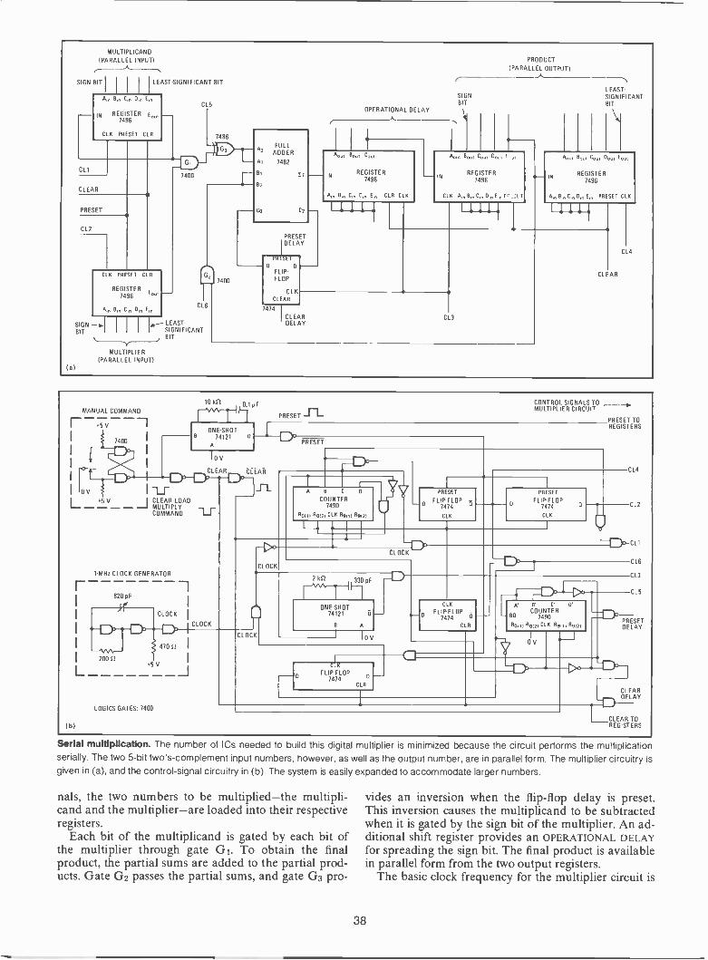
MULTIPLICAND
(PARALLEL INPUT)
SIGN BIT I III I LEAST -SIGNIFICANT BIT
A,,, B,,, C,,, 0,,, E,,,
IN REGISTER Eo
7496
CLK PRESET CLR
CU
CLEAR
PRESET
CL2
CLK PRESET C R
REGISTER7496 °
A,,, B C, 0,E,
rip7400
CL5
7486
21 7400
CL6
SIGN --1,1 I I I IA.- LEAST -BIT SIGNIFICANT
MULTIPLIER(PARALLEL INPUT)
la)
F 62
FULLADDER
7482
CO C2
PRESETDELAY
PFILT0 0
FLIPFLOP
CLKCLEAR
SIGNBIT
OPERATIONAL DELAY
IN
AOut Out COut
REGISTER7496
A, B,,, C,,, 0,,, E, CLR CLK
PRODUCT
(PARALLEL OUTPUT)A
IN
AOUt BOW Coul
REGISTER7496
CLK A,,, B,,, C,,, 0,, E Pr :FAT
I111+
LEAST -SIGNIFICANTBIT
IN
Apo, Bou, Coo, 0,,,,, au,
REGISTER7496
A,,, B,,, C,,, 0,,, E,, PRESET CLK
I 1 ilf
7474 I
CLEARDELAY
CL3
CLEAR
CL4
MANUAL COMMAND
E 75V
7400
kr(
ONE-SHOTB 74121 0
CONTROL SIGNALS TOMULTIPLIER CIRCUIT
PRESET
10V
CLEAR CLEAR
10V I
V_ 1 LLIJELArk_VAD-L_-COMMAND 1..r
1 MHz CLOCK GENERATOR
820 pF
JVvr20012
L
CLOCK I
CLOCK
PRESET
A
COUNT R7490
80111 Rom CLK R9011191,1
PRESET
FLIP FLOP7474
CLK
D
PRESET
FLIP-FLOP7474
CLK
470 SI I
+5 V
LOGICS GATES: 7400
(b)
CLOCK
CLOCK
CLOCK
ig
ONE-SHOT74121 0
A
0 V
-0
CLK
FLIP-FLOP7474
CLR
PRESET TOREGISTERS
'
CLI
CL6
CL3
CL5
C K
FLIP FLOP -7474
CLR
A' B' C'
COUNTERBD 7490
80111 80121 CLK Rg111 89121
0
PRESETDELAY
CLEARDELAY
CLEAR TOREGISTERS
Serial multiplication. The number of ICs needed to build this digital multiplier is minimized because the circuit performs the multiplicationserially. The two 5 -bit two's -complement input numbers, however, as well as the output number, are in parallel form. The multiplier circuitry isgiven in (a), and the control -signal circuitry in (b). The system is easily expanded to accommodate larger numbers.
nals, the two numbers to be multiplied-the multipli-cand and the multiplier-are loaded into their respectiveregisters.
Each bit of the multiplicand is gated by each bit ofthe multiplier through gate 01. To obtain the finalproduct, the partial sums are added to the partial prod-ucts. Gate G2 passes the partial sums, and gate G3 pro-
vides an inversion when the flip-flop delay is preset.This inversion causes the multiplicand to be subtractedwhen it is gated by the sign bit of the multiplier. An ad-ditional shift register provides an OPERATIONAL DELAYfor spreading the sign bit. The final product is availablein parallel form from the two output registers.
The basic clock frequency for the multiplier circuit is
38

1 megahertz. Naturally, a faster clock is needed if big-ger numbers are to be multiplied. The number of clockpulses required to multiply two n -bit numbers (where nincludes the sign bit) is 2n(n-1). Additionally, largernumbers will mean more registers in the multiplier cir-cuitry and more counters in the control -signal circuitry.
Regulating supply voltageall the way down to zeroby Brother Thomas McGaheeDon Bosco Technical School, Boston, Mass.
Precision monolithic voltage regulators make it fairlyeasy to design a high-performance power supply with aminimum of external components. These regulatorshave one general fault, however-they cannot regulateto any voltage lower than their reference, which is usu-ally about 7 v. Sometimes, a voltage divider can be usedto reduce the reference voltage, but if the reference volt-age is reduced below approximately 2 v, good regu-lation can no longer be maintained.
The circuit shown in the figure, on the other hand, al-lows the reference voltage to be adjusted all the waydown to the offset voltage of the regulator's internalop amp. REGULATORI and its associated circuitry forma bias supply that provides a voltage of about -7 V forthe V- terminal of the main regulator (REGULATOR2).Since the noninverting input of this regulator is con-nected to the common ground of the circuit, its refer-ence voltage appears to be + 7 v with respect to thisV -terminal.
(Some minor circuit changes must also be made.)There is a useful rule of thumb to keep in mind to
minimize modification when the multiplier is expanded.Choose the factor 2(n-1) to be the nearest larger integerpower of 2 and then set the extra bits introduced in themultiplicand and the multiplier to zero. 0
There will be a 7-v drop across resistors R2 and R3.When R1 is set to its minimum value, the circuit's out-put voltage will be equal to the reference voltage. If theoutput is measured with respect to the V- terminal ofREGULATOR2, it will be 7 V. But if it is measured withrespect to the common ground, it will be zero.
The maximum voltage available at the output is de-termined by the value of resistor R2. For the componentvalues shown here, the maximum voltage may be setanywhere from 16 to 39 v. But voltages above 30 v willnot be regulated very well because the supply is using a24-v transformer (T2).
The equation for the output voltage is:
VouT = Ri Vs /(R2 + R3)
where V8 is the absolute value of the bias voltage (7 vin this case). The bias supply normally will be produc-ing about 12 milliamperes of current. Under worst -caseconditions, however, it may be required to provide amaximum of 40 mA. Transformer Ti, therefore, shouldbe a 12-v unit capable of supplying at least 50 mA(since REGULATOR) will require some current itself).
The transistor at the output of REGULATOR2 booststhe circuit's output current. Resistor R4 acts as the cur-rent -limiting resistor. 0
IREGULATORS: 723
Tt : 12 V, 300 mA
T2: 24 V. 1.2 ARI: LINEAR POTR2: PC BOARD POT
TDIODES:
3A, 100 V
HEAT SINK
T,
500µF(50 V)
2N3055 0 68 12(1W)
Vc Vo.. Cl.
CS
N. INV INV
REGULATOR2
V COMP
04
( + )
470
10 k52
R2
2.51(2 500µF(35 V)
OUTPUT- 30 V
AT 1A)
DIODES:1A, 50 V
220 µF(35 V)
VouT
REGULATOR,
VREF
N. INV
INV
COMP
R3
1.8 k52(%W, 5%)
470pF
50µF(15 V)
(GND)
Variable supply. This power supply, which employs two IC voltage regulators, produces a regulated output voltage of between 0 and 30 V.REGULATOR, provides the bias voltage for REGULATOR2 so that the latter device can operate with respect to a common ground. The lowestregulated output voltage, then, is approximately zero, rather than the reference voltage of REGULATOR2.
39

Capacitance -coupled logicfills unusual jobsby Stephen R ParelesCook College of Environmental Science, New Brunswick, N.J.
Capacitively coupling logic signals may prove to be asimple way to do several not -so -simple jobs. For in-stance, capacitive coupling can make short work of bi-directional pulse -edge detection, as well as comparisonof an analog signal and a digital signal.
With the circuit of Fig. 1 and a single -trace oscillo-scope, an analog signal and a digital signal can be dis-played at the same time, allowing the two signals to becompared or synchronized. The circuit's output is theanalog signal with superimposed digital cursors.
The capacitor serves as a bidirectional edge -detectorfor the buffered arbitrary logic train. Analog -level tran-sients are produced by the capacitor from this inputlogic train. They are positive for leading pulse edgesand negative for trailing pulse edges.
These transients are then cross -coupled with theanalog signal through resistors that provide cross -cur-rent isolation (100-kilohm resistors are sufficient formost applications). A capacitance of 500 picofarads isideal for slow horizontal sweep rates of up to about 100hertz. Smaller capacitance values should be used forfaster sweep rates to prevent the trailing edges of thetransients from becoming observable.
Capacitive coupling can also be used to perform bidi-rectional edge -detection when a logic -level output is de-sired. The detector circuit, which is drawn in Fig. 2, caneven handle variable pulse widths.
Normally, a 74121 -type one-shot is only triggered bya positive transition at point D, following a low condi-tion at points D and Q. When the input first goes high,point Al goes high. Since point A2 is still high, point Cmomentarily remains -low. When A2 goes low and Chigh, the one-shot is triggered by the positive edge at D.Point B is kept high throughout.
When the input goes low, Al goes low before A2 goeshigh, so that C remains high. Point B, however, is mo-mentarily low. When B goes high again, the one-shot istriggered by the positive edge at C, as before. The tablesin Fig. 2 detail the circuit's operation at key points.
1. Two -signal display. A capacitor simplifies the task of observing two signals on a single -trace oscilloscope. The circuit's output becomesthe analog input with superimposed digital timing cursors. The two 100-kilohm resistors provide the necessary cross -current isolation.
INPUT
OUTPUT
INPUT
ONE SHOT
I--500 p
Al
2 kS2
+5 V
7400
A2
TIME
CIRCUIT OPERATION
POSITIVE INPUT TRANSITION NEGATIVE INPUT TRANSITION
INPUT Al A2 CBOG INPUT Al A2 C B D Cl
tr, 0 0 1 1 1 1 0 1 1 0 1 1 1 0
TRANSITION 1 1 1 0 1 0 0 0 0 0 1 0 0 0
tn+1 1 1 0 1 1 1 ONE-SHOT 0 0 1 1 1 1 ONE-SHOT
74121
OUTPUT
2. Dual edge -detection. Both the leading and trailing edges of the input -pulse train are detected by this capacitively coupled circuit.
40
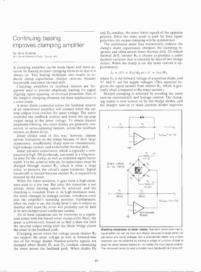
Continuing biasingimproves clamping amplifierby Jerry GraemeBurr -Brown Research Corp . Tucson Ar,;
A clamping amplifier can be made faster and more ac-curate by biasing its zener clamping element so that it isalways on. This biasing technique also results in re-duced clamp capacitance, sharper turn -on, broaderbandwidth, and lower thermal drift.
Clamping amplifiers or feedback limiters are fre-quently used to provide amplitude limiting for signalclipping, signal squaring, or overload protection. One ofthe simplest clamping elements for these applications isa zener diode.
A zener diode connected across the feedback resistorof an operational amplifier will conduct when the op -amp output level reaches the zener voltage. The zeneroverrides the feedback resistor and limits the op -ampoutput swing at the zener voltage. To obtain bipolaramplitude limiting, two zener diodes are generally con-nected, in series -opposing fashion, across the feedbackresistor, as shown in (a).
Zener diodes used in this way, however, imposeserious limitations on the clamp because of their largecapacitance, insufficiently sharp turn -on characteristic,high leakage current, and undesirable thermal drift.
Zener parasitic capacitance, which is typically a com-paratively high 700 picofarads. can result in a long turn -on time for the clamp, as well as restricted signal band-width. For the zener to turn on, its capacitance must becharged through resistor R1, which is often a largevalue, to preserve the circuit's input resistance. Signalbandwidth is limited because resistor R2 is capacitivelyshunted by the zener.
When the zener conducts, it goes from a high -resist-ance state to a low one. But since this transition is notabrupt, sharp limiting cannot be achieved, and theclamping is rounded. Even in its high -resistance state,the zener, through its leakage current, introduces errorinto the amplifier's summing junction. Furthermore,when the zener is on, the clamp level it sets is subject tothermal drift since the zener will probably not be heldat its zero -temperature -coefficient current.
All of these limitations can be overcome to a signifi-cant extent with the biased zener clamp of (b). Here, thezener is continuously biased on so that it does not limitthe op -amp output swing until the diode bridge placesthe zener in the feedback path.
Clamping occurs when the voltage across resistor R2can support the zener voltage as well as forward -biastwo of the bridge diodes. Positive -polarity signals areclamped when diodes D1 and D3 conduct, connectingthe zener across the feedback path. When diodes D2
and D4 conduct, the zener limits signals of the oppositepolarity. Since the same zener is used for both signalpolarities, the output clamping will be symmetrical.
The continuous zener bias dramatically reduces theclamp's shunt capacitance, sharpens the clamping re-sponse, and often means lower thermal drift. To reducethermal drift, resistor R3 is chosen to produce a zenerthermal variation that is canceled by that of two bridgediodes. When the clamp is on, the zener current is ap-proximately:
/z = (V+ + VF)/ R3 or (-v- + VF)/ R3
where VF is the forward voltage of a junction diode, andV+ and V- are the supply voltages. (This equation ne-glects the signal current from resistor R1, which is gen-erally small compared to the zener current.)
Sharper clamping is achieved by avoiding the zenerturn -on characteristic and leakage current. The clamp-ing circuit is now turned on by the bridge diodes, andthe sharper turn -on of these junction diodes improves
Whetting sharpness of zener clamp. Standard zener-type clamp-ing amplifier (a) can be slow and sloppy because of large zener ca-pacitance and zener leakage. But a dramatically faster and crisperresponse can be obtained by adding a bridge of junction diodes tokeep the zener always biased on, no matter the input signal polarityThe improved clamp (b) also provides more bandwidth and less drift
41
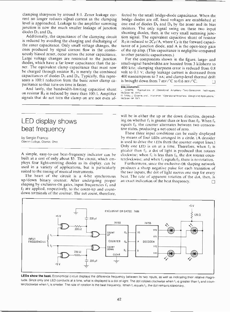
clamping sharpness by around 8:1. Zener leakage cur-rent no longer reduces signal current as the clampinglevel is approached. Leakage to the amplifier summingjunction is now the much smaller leakage of junctiondiodes D1 and D4.
Additionally, the capacitance of the clamping circuitis reduced by avoiding the charging and discharging ofthe zener capacitance. Only small voltage changes, theones produced by signal current flow in the contin-uously biased zener, occur across the zener capacitance.Large voltage changes are restricted to the junctiondiodes, which have a far lower capacitance than the ze-ner. The equivalent clamp capacitance that must nowbe charged through resistor R1 is merely the combinedcapacitances of diodes D1 and D.1. Typically, this repre-sents a 100: 1 reduction from the basic zener clamp ca-pacitance so that turn -on time is faster.
And lastly, the bandwidth -limiting capacitive shunton resistor R2 is reduced by more than 100:1. Amplifiersignals that do not turn the clamp on are not even af-
fected by the small bridge -diode capacitance. When thebridge diodes are off, fixed voltages are established atone end of diodes DI and D4 by the zener and its biasresistors. The only signal swing on these two inputshunting diodes, then, is the very small summing junc-tion signal. The equivalent capacitive shunt of resistorR2 is reduced to 2CF/A, where CF is the forward capaci-tance of a junction diode, and A is the open -loop gainof the op amp. (This capacitance is negligible comparedto other parasitic capacitances.)
For the components shown in the figure, large- andsmall -signal bandwidths are boosted from 3 kilohertz to400 kHz; clamping sharpness error is reduced from 0.8volt to 0.1 v; clamp leakage current is decreased from400 nanoamperes to 7 nA; and clamp -level thermal driftis brought down from 7 mv/°C to 0.6 mv/°C.BIBLIOGRAPHY:J Graeme. "Applications of Operational Amplifiers-Third-Generation Techniques.McGraw-Hill. 1973G. Tobey. J Graeme. and L Huelsman, "Operational Amplifiers-Design and Applications."McGraw-Hill, 1971
LED display showsbeat frequencyby Sergio FrancoOberlin College, Oberlin, Ohio
A simple, easy -to -use beat -frequency indicator can hebuilt at a cost of only about $5. The circuit, which em-ploys four light -emitting diodes as its display, can beused in a variety of applications, but is particularlysuited to the tuning of musical instruments.
The heart of the circuit is a 4 -bit synchronousup/down binary counter. After undergoing propershaping by exclusive -OR gates, input frequencies fi andf2 are applied, respectively, to the count -up and count-down terminals of the counter. The net count, therefore,
will be in either the up or the down direction, depend-ing on whether f1 is greater than or less than f2. When f1equals 12, the counter alternates between two consecu-tive states, producing a net count of zero.
These three input conditions can be easily displayedby means of four LEDs arranged in a circle. (A decoderis used to drive the LEDs from the counter output lines.)Only one LED is on at a time. Therefore, when f1 isgreater than 12, a dot of light is produced that rotatesclockwise; when fl is less than 12, the dot rotates coun-terclockwise; and when fi equals f2, there is no rotation.
Furthermore, since the exclusive -OR shaping networkproduces a sharp negative pulse for each transition ofthe two inputs, the dot of light moves one step for everybeat. The rate of apparent rotation of the dot, then, isan exact indication of the beat frequency.
INPUTFREQUENCIES
+5 V
+5 V
+5 V
4- EXCLUSIVE OR GATES 7486
LEDs show the beat. Economical circuit displays the difference frequency between its two inputs, as well as indicating their relative magni-tude. Since only one LED conducts at a time, what is displayed is a dot of light. The dot rotates clockwise when f is greater than f2 and coun-terclockwise when f 1 is smaller. The rate of rotation is the beat frequency. When f, equals f2, the dot remains stationary.
42
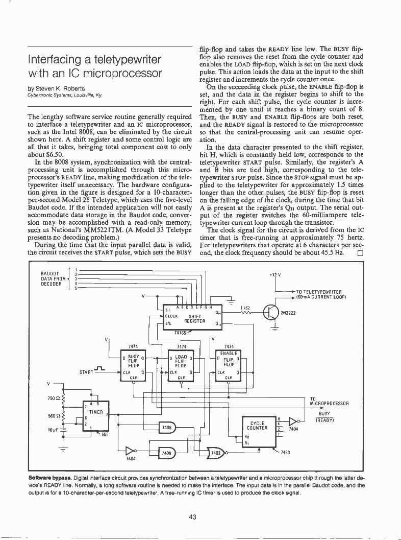
Interfacing a teletypewriterwith an IC microprocessorby Steven K. RobertsCybertronic Systems, Louisville, Ky.
The lengthy software service routine generally requiredto interface a teletypewriter and an lc microprocessor,such as the Intel 8008, can be eliminated by the circuitshown here. A shift register and some control logic areall that it takes, bringing total component cost to onlyabout $6.50.
In the 8008 system, synchronization with the central -processing unit is accomplished through this micro-processor's READY line, making modification of the tele-typewriter itself unnecessary. The hardware configura-tion given in the figure is designed for a 10 -character -per -second Model 28 Teletype, which uses the five -levelBaudot code. If the intended application will not easilyaccommodate data storage in the Baudot code, conver-sion may be accomplished with a read-only memory,such as National's MM5221TM. (A Model 33 Teletypepresents no decoding problem.)
During the time that the input parallel data is valid,the circuit receives the START pulse, which sets the BUSY
flip-flop and takes the READY line low. The BUSY flip-flop also removes the reset from the cycle counter andenables the LOAD flip-flop, which is set on the next clockpulse. This action loads the data at the input to the shiftregister and increments the cycle counter once.
On the succeeding clock pulse, the ENABLE flip-flop isset, and the data in the register begins to shift to theright. For each shift pulse, the cycle counter is incre-mented by one until it reaches a binary count of 8.Then, the BUSY and ENABLE flip-flops are both reset,and the READY signal is restored to the microprocessorso that the central -processing unit can resume oper-ation.
In the data character presented to the shift register,bit H, which is constantly held low, corresponds to theteletypewriter START pulse. Similarly, the register's Aand B bits are tied high, corresponding to the tele-typewriter STOP pulse. Since the STOP signal must be ap-plied to the teletypewriter for approximately 1.5 timeslonger than the other pulses, the BUSY flip-flop is reseton the falling edge of the clock, during the time that bitA is present at the register's QH output. The serial out-put of the register switches the 60 -milliampere tele-typewriter current loop through the transistor.
The clock signal for the circuit is deriVed from the ICtimer that is free -running at approximately 75 hertz.For teletypewriters that operate at 6 characters per sec-ond, the clock frequency should be about 45.5 Hz. 0
BAUDOTDATA FROMDECODER
750 S2
560 S2
10µF
2
3
4
START
7
6
2
TIMER
V
7474
D BUSYFLIP-FLOP
CLK 0
CLR
A B CS.I.
CLOCK
SiL
SHIFTREGISTER
H
QH
74165
7474
LOADFLIP-FLOP
CLK U
CLR
7474
ENABLE
FLIP- a '--FLOP
CLK U -40CLR
+12 V
0 TO TELETYPEWRITER(60-mA CURRENT LOOP)
2N2222
TOMICROPROCESSOR
555
7404
CYCLECOUNTER
Ro
4
2 7404
7493
BUSY
(READY)
Software bypass. Digital interface circuit provides synchronization between a teletypewriter and a microprocessor chip through the latter de-vice's READY line. Normally, a long software routine is needed to make the interface. The input data is in the parallel Baudot code, and theoutput is for a 10 -character -per -second teletypewriter. A free -running IC timer is used to produce the clock signal.
43
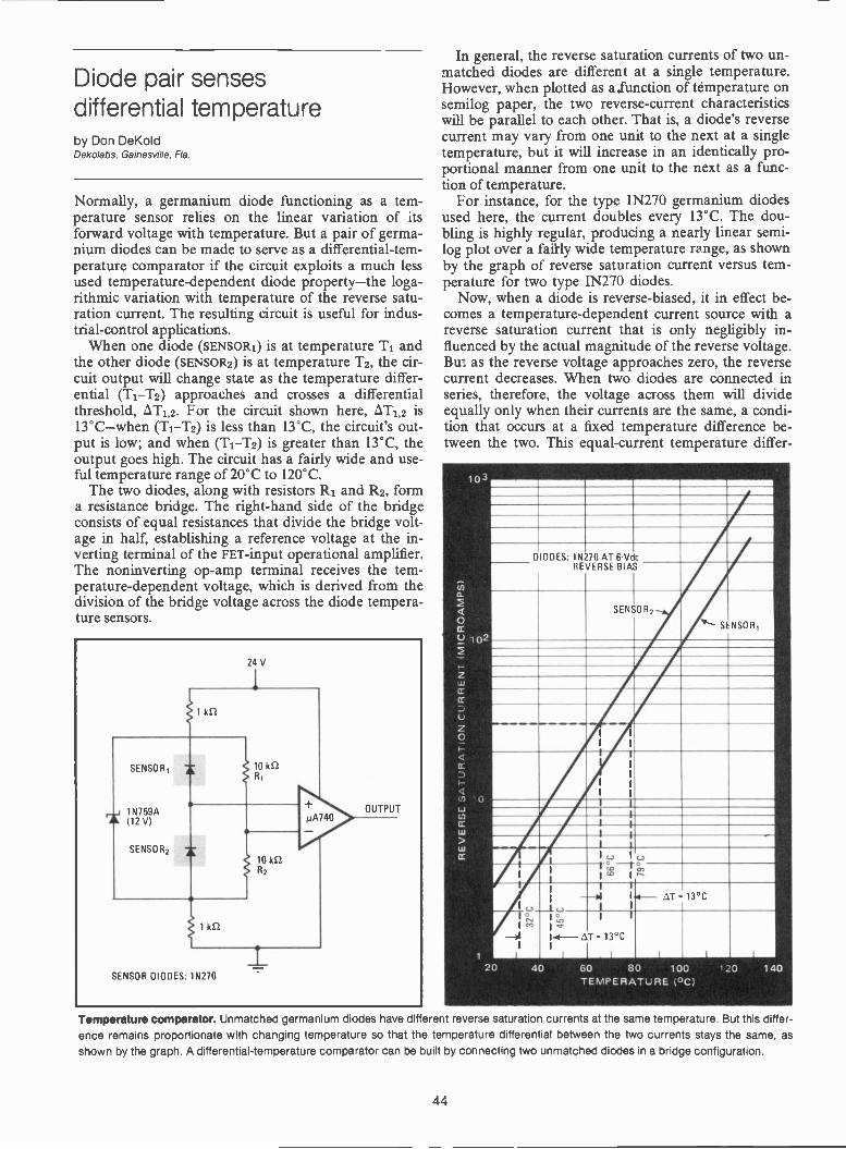
Diode pair sensesdifferential temperatureby Don DeKoldDekolabs, Gainesville, Fla.
Normally, a germanium diode functioning as a tem-perature sensor relies on the linear variation of itsforward voltage with temperature. But a pair of germa-nium diodes can be made to serve as a differential -tem-perature comparator if the circuit exploits a much lessused temperature -dependent diode property-the loga-rithmic variation with temperature of the reverse satu-ration current. The resulting circuit is useful for indus-trial -control applications.
When one diode (sENsoRi) is at temperature Ti andthe other diode (SENSOR2) is at temperature Tz, the cir-cuit output will change state as the temperature differ-ential (T1 -T2) approaches and crosses a differentialthreshold, AT1,2. For the circuit shown here, ST1,2 is13°C-when (T1 -T2) is less than 13°C, the circuit's out-put is low; and when (Ti -T2) is greater than 13°C, theoutput goes high. The circuit has a fairly wide and use-ful temperature range of 20°C to 120°C.
The two diodes, along with resistors R1 and Rz, forma resistance bridge. The right-hand side of the bridgeconsists of equal resistances that divide the bridge volt-age in half, establishing a reference voltage at the in-verting terminal of the FET-input operational amplifier.The noninverting op -amp terminal receives the tem-perature -dependent voltage, which is derived from thedivision of the bridge voltage across the diode tempera-ture sensors.
In general, the reverse saturation currents of two un-matched diodes are different at a single temperature.However, when plotted as a .function of temperature onsemilog paper, the two reverse -current characteristicswill be parallel to each other. That is, a diode's reversecurrent may vary from one unit to the next at a singletemperature, but it will increase in an identically pro-portional manner from one unit to the next as a func-tion of temperature.
For instance, for the type 1N270 germanium diodesused here, the current doubles every 13°C. The dou-bling is highly regular, producing a nearly linear semi -log plot over a faitly wide temperature range, as shownby the graph of reverse saturation current versus tem-perature for two type IN270 diodes.
Now, when a diode is reverse -biased, it in effect be-comes a temperature -dependent current source with areverse saturation current that is only negligibly in-fluenced by the actual magnitude of the reverse voltage.Bus as the reverse voltage approaches zero, the reversecurrent decreases. When two diodes are connected inseries, therefore, the voltage across them will divideequally only when their currents are the same, a condi-tion that occurs at a fixed temperature difference be-tween the two. This equal -current temperature differ -
103
DIODES: 1N270REVERSE
AT 6-VdcBIAS
2<
oCC
(-1_
2102
SENSOR2
'- SENSOR,
Z Al.kiifif
UZo 4VAIM=
I
II I
I
<(rDE-4ca
U0 I I
I ICaCC
U.I
I I
I I> I I
U.I
Cr I I c..) I urZs, -11r3I '''' I
I
I1
I I-a 1..-I I
AT = 13°C
'?..,
IM--0
II
.)
I Tr,1 ..*
1-4- ATI
I
I I
=13°C
I I I
20 40 60 80 100TEMPERATURE 1°C)
' 20 140
Temperature comparator. Unmatched germanium diodes have different reverse saturation currents at the same temperature. But this differ-ence remains proportionate with changing temperature so that the temperature differential between the two currents stays the same, asshown by the graph. A differential -temperature comparator can be built by connecting two unmatched diodes in a bridge configuration.
44
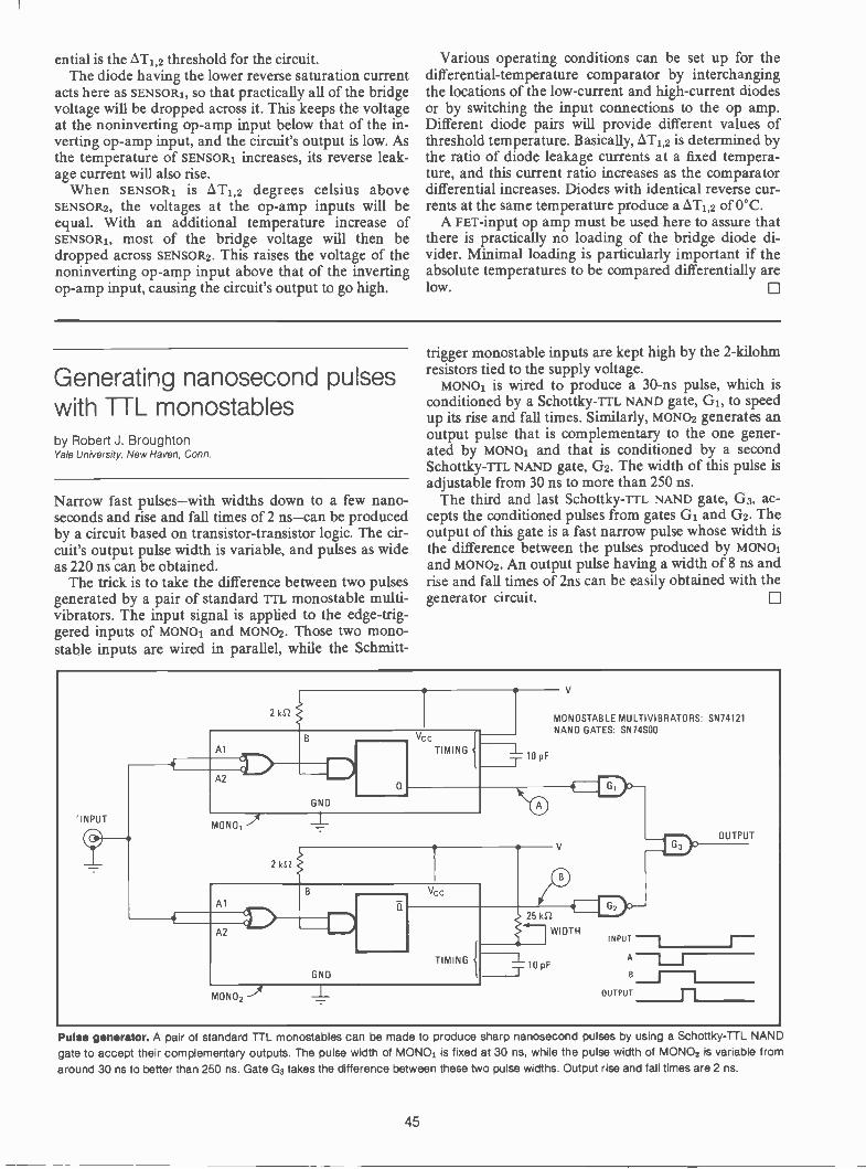
ential is the AT1,2 threshold for the circuit.The diode having the lower reverse saturation current
acts here as SENSOR', so that practically all of the bridgevoltage will be dropped across it. This keeps the voltageat the noninverting op -amp input below that of the in-verting op -amp input, and the circuit's output is low. Asthe temperature of SENSOR' increases, its reverse leak-age current will also rise.
When SENSOR' is AT1,2 degrees celsius aboveSENSOR2, the voltages at the op -amp inputs will beequal. With an additional temperature increase ofSENSOR', most of the bridge voltage will then bedropped across SENSOR2. This raises the voltage of thenoninverting op -amp input above that of the invertingop -amp input, causing the circuit's output to go high.
Various operating conditions can be set up for thedifferential -temperature comparator by interchangingthe locations of the low -current and high -current diodesor by switching the input connections to the op amp.Different diode pairs will provide different values ofthreshold temperature. Basically, AT1,2 is determined bythe ratio of diode leakage currents at a fixed tempera-ture, and this current ratio increases as the comparatordifferential increases. Diodes with identical reverse cur-rents at the same temperature produce a AT1,2 of 0°C.
A FET-input op amp must be used here to assure thatthere is practically no loading of the bridge diode di-vider. Minimal loading is particularly important if theabsolute temperatures to be compared differentially arelow.
Generating nanosecond pulseswith TTL monostablesby Robert J. BroughtonYale University, New Haven, Conn.
Narrow fast pulses-with widths down to a few nano-seconds and rise and fall times of 2 ns-can be producedby a circuit based on transistor -transistor logic. The cir-cuit's output pulse width is variable, and pulses as wideas 220 ns can be obtained.
The trick is to take the difference between two pulsesgenerated by a pair of standard Tit monostable multi -vibrators. The input signal is applied to the edge -trig-gered inputs of MONO1 and MONO2. Those two mono -stable inputs are wired in parallel, while the Schmitt -
trigger monostable inputs are kept high by the 2-kilohmresistors tied to the supply voltage.
MONO1 is wired to produce a 30-ns pulse, which isconditioned by a Schottky -Tit NAND gate, G1, to speedup its rise and fall times. Similarly, MONO2 generates anoutput pulse that is complementary to the one gener-ated by MONO1 and that is conditioned by a secondSchottky -Tit NAND gate, G2. The width of this pulse isadjustable from 30 ns to more than 250 ns.
The third and last Schottky-rm.. NAND gate, G3, ac-cepts the conditioned pulses from gates GI and G2. Theoutput of this gate is a fast narrow pulse whose width isthe difference between the pulses produced by MONO1and MONO2. An output pulse having a width of 8 ns andrise and fall times of 2ns can be easily obtained with thegenerator circuit.
'INPUT
2
Al
A2
GND
VccTIMING T10 pF
MONOSTABLE MULTIVIBRATORS: SN74121NAND GATES: SN74S00
MONO,
2 IcS1
Al
A20 -D
GND
VC C
TIMING
Is
425 kg -2
WIDTHINPUT
UP OUTPUT
_L A -Lio pF
MONO2 OUTPUT
Pulse generator. A pair of standard TTL monostables can be made to produce sharp nanosecond pulses by using a Schottky-TTL NANDgate to accept their complementary outputs. The pulse width of MONO1 is fixed at 30 ns, while the pulse width of MONO2 is variable fromaround 30 ns to better than 250 ns. Gate G3 takes the difference between these two pulse widths. Output rise and fall times are 2 ns.
45
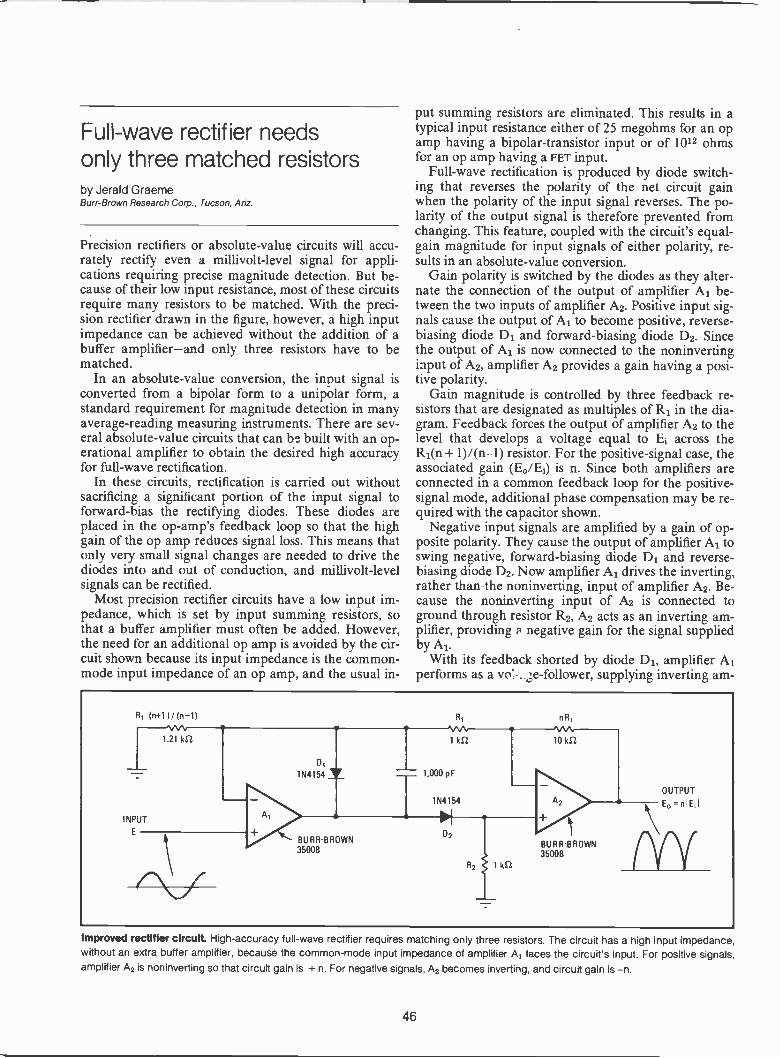
Full -wave rectifier needsonly three matched resistorsby Jerald GraemeBurr -Brown Research Corp., Tucson, Ariz.
Precision rectifiers or absolute -value circuits will accu-rately rectify even a millivolt -level signal for appli-cations requiring precise magnitude detection. But be-cause of their low input resistance, most of these circuitsrequire many resistors to be matched. With the preci-sion rectifier drawn in the figure, however, a high inputimpedance can be achieved without the addition of abuffer amplifier-and only three resistors have to bematched.
In an absolute -value conversion, the input signal isconverted from a bipolar form to a unipolar form, astandard requirement for magnitude detection in manyaverage -reading measuring instruments. There are sev-eral absolute -value circuits that can he built with an op-erational amplifier to obtain the desired high accuracyfor full -wave rectification.
In these circuits, rectification is carried out withoutsacrificing a significant portion of the input signal toforward -bias the rectifying diodes. These diodes areplaced in the op -amp's feedback loop so that the highgain of the op amp reduces signal loss. This means thatonly very small signal changes are needed to drive thediodes into and out of conduction, and millivolt -levelsignals can be rectified.
Most precision rectifier circuits have a low input im-pedance, which is set by input summing resistors, sothat a buffer amplifier must often be added. However,the need for an additional op amp is avoided by the cir-cuit shown because its input impedance is the common -
mode input impedance of an op amp, and the usual in-
put summing resistors are eliminated. This results in atypical input resistance either of 25 megohms for an opamp having a bipolar -transistor input or of 1012 ohmsfor an op amp having a FET input.
Full -wave rectification is produced by diode switch-ing that reverses the polarity of the net circuit gainwhen the polarity of the input signal reverses. The po-larity of the output signal is therefore prevented fromchanging. This feature, coupled with the circuit's equal -
gain magnitude for input signals of either polarity, re-sults in an absolute -value conversion.
Gain polarity is switched by the diodes as they alter-nate the connection of the output of amplifier Al be-tween the two inputs of amplifier A2. Positive input sig-nals cause the output of Al to become positive, reverse -
biasing diode D1 and forward -biasing diode D2. Sincethe output of Al is now connected to the noninvertinginput of A2, amplifier A2 provides a gain having a posi-tive polarity.
Gain magnitude is controlled by three feedback re-sistors that are designated as multiples of R1 in the dia-gram. Feedback forces the output of amplifier A2 to thelevel that develops a voltage equal to E1 across theIti(n + 1)/(n-1) resistor. For the positive -signal case, theassociated gain (E./E1) is n. Since both amplifiers areconnected in a common feedback loop for the positive -signal mode, additional phase compensation may be re-quired with the capacitor shown.
Negative input signals are amplified by a gain of op-posite polarity. They cause the output of amplifier Al toswing negative, forward -biasing diode D1 and reverse -
biasing diode D2. Now amplifier Al drives the inverting,rather than the noninverting, input of amplifier A2. Be-cause the noninverting input of A2 is connected toground through resistor R2, A2 acts as an inverting am-plifier, providing a negative gain for the signal suppliedby Al.
With its feedback shorted by diode D1, amplifier Alperforms as a vo' 3e -follower, supplying inverting am -
R1 (n+11/(n-1(
1.21 ks2
INPUT
E
Al
DI1N4154
BURR -BROWN3500B
R1
1 IcE2 10 l(S2
T1 000 pF
1N4154
02
1 1(2
A2
111
BURR -BROWN3500B
OUTPUT
Eo-nlE,1
ME_
Improved rectifier circuit. High -accuracy full -wave rectifier requires matching only three resistors. The circuit has a high input impedance,without an extra buffer amplifier, because the common -mode input impedance of amplifier Al faces the circuit's input. For positive signals,amplifier A2 is noninverting so that circuit gain is + n. For negative signals, A2 becomes inverting, and circuit gain is -n.
46
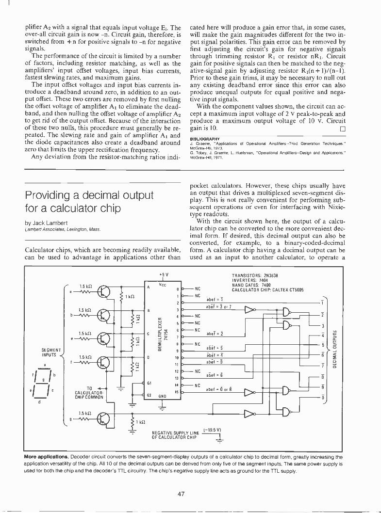
plifier A2 with a signal that equals input voltage E1. Theover-all circuit gain is now -n. Circuit gain, therefore, isswitched from +n for positive signals to -n for negativesignals.
The performance of the circuit is limited by a numberof factors, including resistor matching, as well as theamplifiers' input offset voltages, input bias currents,fastest slewing rates, and maximum gains.
The input offset voltages and input bias currents in-troduce a deadband around zero, in addition to an out-put offset. These two errors are removed by first nullingthe offset voltage of amplifier A1 to eliminate the dead-
band, and then nulling the offset voltage of amplifier A2to get rid of the output offset. Because of the interactionof these two nulls, this procedure must generally be re-peated. The slewing rate and gain of amplifier Al andthe diode capacitances also create a deadband aroundzero that limits the upper rectification frequency.
Any deviation from the resistor -matching ratios indi-
cated here will produce a gain error that, in some cases,will make the gain magnitudes different for the two in-put signal polarities. This gain error can be removed byfirst adjusting the circuit's gain for negative signalsthrough trimming resistor R1 or resistor nRi. Circuitgain for positive signals can then be matched to the neg-ative -signal gain by adjusting resistor Ri(n + 1)/(n-1).Prior to these gain trims, it may be necessary to null outany existing deadband error since this error can alsoproduce unequal outputs for equal positive and nega-tive input signals.
With the component values shown, the circuit can ac-cept a maximum input voltage of 2 v peak -to -peak andproduce a maximum output voltage of 10 v. Circuitgain is 10.
BIBLIOGRAPHYJ. Graeme. "Applications of Operational Amplifiers-Third Generation Techniques,"McGraw-Hill, 1973.G. Tobey, J. Graeme, L. Huelsman, "Operational Amplifiers-Design and Applications,"McGraw-Hill, 1971.
Providing a decimal outputfor a calculator chipby Jack LambertLambert Associates, Lexington, Mass.
Calculator chips, which are becoming readily available,can be used to advantage in applications other than
pocket calculators. However, these chips usually havean output that drives a multiplexed seven -segment dis-play. This is not really convenient for performing sub-sequent operations or even for interfacing with Nixie -type readouts.
With the circuit shown here, the output of a calcu-lator chip can be converted to the more convenient dec-imal form. If desired, this decimal output can also beconverted, for example, to a binary -coded -decimalform. A calculator chip having a decimal output can beused as an input to another calculator, to operate a
SEGMENTINPUTS
a
fl b
elI
c
d
1.5 k
+5 V
V c c
0
1
2
1 kS2
0 NCa
0 NC
0
1.5 k1-2 3 0
NCb4 0-
CC0.1X 5 0 NC
1.5 1(12
LLI
6 0 NC0- 407
8 D- NC9 0
1.5 kS2 10
11 D
12 D- NC13 D
TO
C G114 D NC4-
CALCULATOR -CHIP COMMON
G2 GND15 D
C
1.51(2
TRANSISTORS: 2N3638INVERTERS: 7404NANO GATES: 7400CALCULATOR CHIP: CALTEX CT5005
abet = 1
abet = 3 or 7
abet = 2
abet = 5
abet
abet = 9
abet = 6
abet = 0 or 8
1 kf2
(-19.5NEGATIVE SUPPLY LINEOF CALCULATOR CHIP -I
More applications. Decoder circuit converts the seven -segment -display outputs of a calculator chip to decimal form, greatly increasing theapplication versatility of the chip. All 10 of the decimal outputs can be derived from only five of the segment inputs. The same power supply is
used for both the chip and the decoder's TTL circuitry. The chip's negative supply line acts as ground for the TTL supply.
47
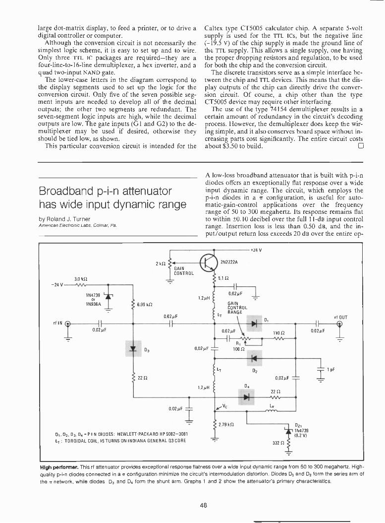
large dot-matrix display, to feed a printer, or to drive adigital controller or computer.
Although the conversion circuit is not necessarily thesimplest logic scheme, it is easy to set up and to wire.Only three nt IC packages are required-they are afour -line -to -16 -line demultiplexer, a hex inverter, and aquad two -input NAND gate.
The lower-case letters in the diagram correspond tothe display segments used to set up the logic for theconversion circuit. Only five of the seven possible seg-ment inputs are needed to develop all of the decimaloutputs; the other two segments are redundant. Theseven -segment logic inputs are high, while the decimaloutputs are low. The gate inputs (G1 and G2) to the de -multiplexer may be used if desired, otherwise theyshould be tied low, as shown.
This particular conversion circuit is intended for the
Caltex type CT5005 calculator chip. A separate 5 -voltsupply is used for the ni ics, but the negative line(-19.5 v) of the chip supply is made the ground line ofthe rit supply. This allows a single supply, one havingthe proper dropping resistors and regulation, to be usedfor both the chip and the conversion circuit.
The discrete transistors serve as a simple interface be-tween the chip and TTL devices. This means that the dis-play outputs of the chip can directly drive the conver-sion circuit. Of course, a chip other than the typeCT5005 device may require other interfacing.
The use of the type 74154 demultiplexer results in acertain amount of redundancy in the circuit's decodingprocess. However, the demultiplexer does keep the wir-ing simple, and it also conserves board space without in-creasing parts cost significantly. The entire circuit costsabout $3.50 to build. 0
Broadband p-i-n attenuatorhas wide input dynamic rangeby Roland J. TurnerAmerican Electronic Labs, Colmar, Pa.
A low -loss broadband attenuator that is built with p-i-ndiodes offers an exceptionally flat response over a wideinput dynamic range. The circuit, which employs thep-i-n diodes in a Tr configuration, is useful for auto-matic -gain -control applications over the frequencyrange of 50 to 300 megahertz. Its response remains flatto within ±0.10 decibel over the full 11 -dB input controlrange. Insertion loss is less than 0.50 dB, and the in-put/output return loss exceeds 20 dB over the entire op-
-24 V
rf IN
3.0 kS2
1N4739Or
1N936A
0 02 pF
6.99 kS2
03
22 1-2
2 kS2 4GAINCONTROL
0.02pF
0 02 pF
D1, 02, D3, D4 = P -I -N DIODES: HEWLETT-PACKARD HP 5082-3081
LT: TOROIDAL COIL, 15 TURNS ON INDIANA GENERAL 03 CORE
D2
2N2222A
5.1 1?,
+24 V
0 02pF1.2µN
GAINCONTROLRANGE
0.02pF
1.2pH 04
Vc
2.79 kS2
0.02 pF
22 S2
LT
332 12
Ozi1N4739(9.2 VI
0 02pF
1 pF
rf OUT
High performer. This rf attenuator provides exceptional response flatness over a wide input dynamic range from 50 to 300 megahertz. Highquality p-i-n diodes connected in a 7 configuration minimize the circuit's intermodulation distortion. Diodes DI and D2 form the series arm ofthe IT network, while diodes D3 and D4 form the shunt arm. Graphs 1 and 2 show the attenuator's primary characteristics.
48
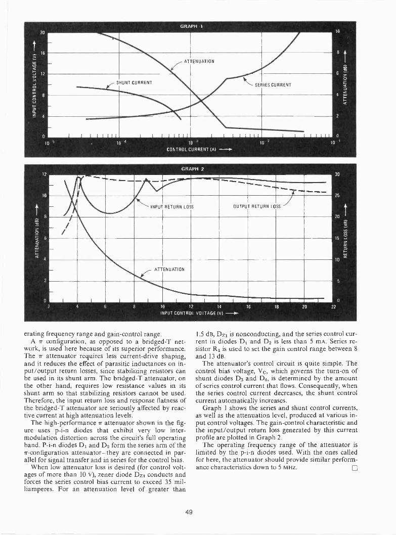
GRAPH 120 10
1611111111VAIMMI 8
12
ATTENUATION
1111=
0 11111111=111 111111M111 0
10 5 10 4 10 3 10 210
CONTROL CURRENT (A) --I.
4
2
GRAPH 212 30
IE61111------ Fr411___ all
..........................
......... ....2510
INPUT RETURN LOSS OUTPUT RETURN LOSS
t20iTi Ez /c, /--r-
6
0111 aC,7
15<=zLu1-r -a
4 &M -,zcc=
cc10
2
ATTENUATION
ii\-
s() iOnliMMI 6
2 4 6 8 10 12 14 16 18 20 ??
INPUT CONTROL VOLTAGE (V) --4.-
erating frequency range and gain -control range.A 7T configuration, as opposed to a bridged -T net-
work, is used here because of its superior performance.The 7 attenuator requires less current -drive shaping,and it reduces the effect of parasitic inductances on in-put/output return losses, since stabilizing resistors canbe used in its shunt arm. The bridged -T attenuator, onthe other hand, requires low resistance values in itsshunt arm so that stabilizing resistors cannot be used.Therefore, the input return loss and response flatness ofthe bridged -T attenuator are seriously affected by reac-tive current at high attenuation levels.
The high-performance it attenuator shown in the fig-ure uses p-i-n diodes that exhibit very low inter -modulation distortion across the circuit's full operatingband. P-i-n diodes D1 and D2 form the series arm of the1r -configuration attenuator-they are connected in par-allel for signal transfer and in series for the control bias.
When low attenuator loss is desired (for control volt-ages of more than 10 v), zener diode Dz1 conducts andforces the series control bias current to exceed 35 mil-liamperes. For an attenuation level of greater than
1.5 dB, Dzi is nonconducting, and the series control cur-rent in diodes D1 and D2 is less than 5 mA. Series re-sistor R1 is used to set the gain control range between 8and 13 dB.
The attenuator's control circuit is quite simple. Thecontrol bias voltage, Vc, which governs the turn -on ofshunt diodes D3 and D4, is determined by the amountof series control current that flows. Consequently, whenthe series control current decreases, the shunt controlcurrent automatically increases.
Graph 1 shows the series and shunt control currents,as well as the attenuation level, produced at various in-put control voltages. The gain -control characteristic andthe input/output return loss generated by this currentprofile are plotted in Graph 2.
The operating frequency range of the attenuator islimited by the p-i-n diodes used. With the ones calledfor here, the attenuator should provide similar perform-ance characteristics down to 5 MHz.
49

IC timer and voltage doublerform a dc -dc converterby Todd GartnerMotorola Inc., Automotive Research & Development, Franklin Park, Ill.
A dc -dc converter in which an IC timer serves as a free -running relaxation oscillator is ideal for poweringop amps in battery -operated equipment or whenever asingle positive supply is all that's available. Further-more, the converter develops an output voltage of -15 vthat is regulated to within ± 1% for load currents of up to30 milliamperes. The circuit's no-load current is 11 mA.
The free -running frequency of the timer is deter-mned by resistors RA and RB and capacitor Gr. Theoutput from the timer is used to drive the voltage -doubler network consisting of diodes D1 through D4and capacitors C1 through C4.
Without the feedback connection between the outputof the voltage doubler and the reset input of the timer,the circuit's output under a no-load condition will floatto about 30 v minus four diode voltage drops. With thefeedback connection, the voltage divider formed bydiodes D5 and D6 and resistors R1 and R2 places a 0.7-v
voltage at the timer's reset input when the negative out-put voltage equals the positive input supply voltage inmagnitude.
If the output voltage becomes more negative than-15 v, the timer's oscillation is inhibited, and therefore,the drive signal to the voltage doubler is removed. Thistype of circuit action provides switching -mode regu-lation of the output voltage.
The voltage doubler deserves a closer look because itmay not be immediately apparent how it works. Whenthe timer's output goes positive, capacitor Cl is chargedthrough diode D1, and diode D2 is reverse -biased.When the timer's output becomes negative, some of thecharge on capacitor C1 is transferred to capacitor C2through diode D2, and diode D1 is now reverse -biased.
As the output from the timer swings positive again,capacitor C3 charges through capacitor C2 and diode D3to approximately twice the supply voltage. For thetimer's negative output swing, this charge is transferredto capacitor C4 via diode D4, doubling the output volt-age from the timer. Such a voltage -doubler arrange-ment requires the driving source to supply, as well assink, current.
The output voltage of the dc -dc converter will trackthe input supply voltage with reasonable accuracy. If re-sistors R1 and R2 are replaced by a single 100-kilohmpotentiometer, the output voltage can be made contin-
1 a2,
10 kS2
+15-V SUPPLY
CT - 0.01AF
vccDISCHARGE RESET
TIMER
THRESHOLD OUTPUT
TRIGGER
GNU
RI
50 kS2
R2
50 kS2 D506
MOTOROLAMC15555
ALL DIODES: 1N914
22µF
D1 V
14
02
+C322µF
03 04
C2 22µF C4 100µF
OUTPUT-15 V(30 mA)
For op amps. This dc -dc converter produces a -15-volt output from a + 15-V supply input. The IC timer, which is wired as a free -runningrelaxation oscillator, drives a voltage doubler. The timer is reset so that its output is inhibited if the converter's output tries to go more negativethan -15 V. The converter's output is regulated to within ±1% for load currents of up' o 30 milliamperes.
50
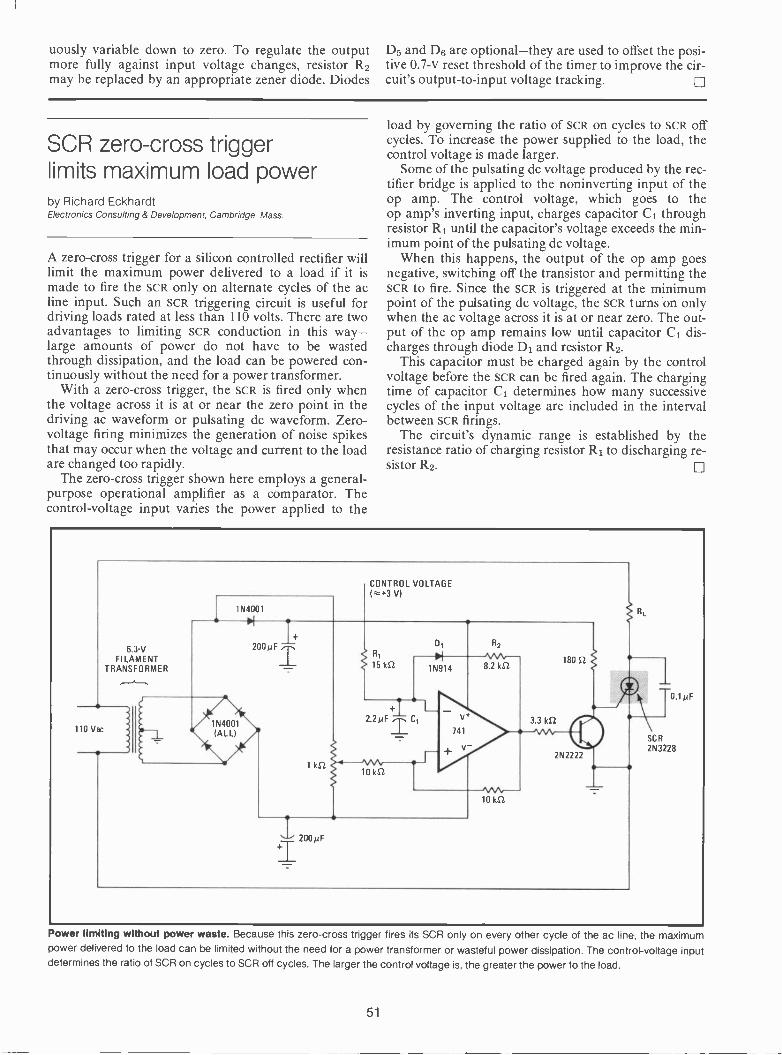
uously variable down to zero. To regulate the outputmore fully against input voltage changes, resistor R2may be replaced by an appropriate zener diode. Diodes
D5 and D6 are optional-they are used to offset the posi-tive 0.7-v reset threshold of the timer to improve the cir-cuit's output -to -input voltage tracking.
SCR zero -cross triggerlimits maximum load powerby Richard EckhardtElectronics Consulting & Development, Cambridge, Mass.
A zero -cross trigger for a silicon controlled rectifier willlimit the maximum power delivered to a load if it ismade to fire the SCR only on alternate cycles of the acline input. Such an SCR triggering circuit is useful fordriving loads rated at less than 110 volts. There are twoadvantages to limiting SCR conduction in this way-large amounts of power do not have to be wastedthrough dissipation, and the load can be powered con-tinuously without the need for a power transformer.
With a zero -cross trigger, the SCR is fired only whenthe voltage across it is at or near the zero point in thedriving ac waveform or pulsating dc waveform. Zero-voltage firing minimizes the generation of noise spikesthat may occur when the voltage and current to the loadare changed too rapidly.
The zero -cross trigger shown here employs a general-purpose operational amplifier as a comparator. Thecontrol -voltage input varies the power applied to the
load by governing the ratio of SCR on cycles to SCR offcycles. To increase the power supplied to the load, thecontrol voltage is made larger.
Some of the pulsating dc voltage produced by the rec-tifier bridge is applied to the noninverting input of theop amp. The control voltage, which goes to theop amp's inverting input, charges capacitor Ci throughresistor RI until the capacitor's voltage exceeds the min-imum point of the pulsating dc voltage.
When this happens, the output of the op amp goesnegative, switching off the transistor and permitting theSCR to fire. Since the SCR is triggered at the minimumpoint of the pulsating dc voltage, the SCR turns 'on onlywhen the ac voltage across it is at or near zero. The out-put of the op amp remains low until capacitor Ci dis-charges through diode D1 and resistor R2.
This capacitor must be charged again by the controlvoltage before the SCR can be fired again. The chargingtime of capacitor C1 determines how many successivecycles of the input voltage are included in the intervalbetween SCR firings.
The circuit's dynamic range is established by theresistance ratio of charging resistor R1 to discharging re-sistor R2.
6.3-VFILAMENT
TRANSFORMER
110 Vac
1N4001
PI
CONTROL VOLTAGE(r+3
200pF
1 kS2
15 kS2
2.2pF c,
10 kC2
1N914
v+
741
V
200 pF
R2
8.2 kS2.
10 k52
3.3 k.S-2.
180
g.,402N2222
00.1µF
SCR
2N3228
Power limiting without power waste. Because this zero -cross trigger fires its SCR only on every other cycle of the ac line, the maximumpower delivered to the load can be limited without the need for a power transformer or wasteful power dissipation. The control -voltage inputdetermines the ratio of SCR on cycles to SCR off cycles. The larger the control voltage is, the greater thepower to the load.
51

Phase -locked loopincludes lock indicatorby J.A. Connelly and G.E. PrescottGeorgia Institute of Technology, Atlanta, Ga.
One problem with phase -locked loops is that it's oftenhard to tell exactly when the loop is locked to the inputsignal. In many applications, it would be very useful toinclude a lock indicator in a phase -locked loop to dis-play the state of the loop.
For example, in automatic test equipment, the lockindicator would afford a simple, yet efficient, way tomeasure the tracking and capture ranges of a phase -locked loop. Also, various low-pass filter configurationscould be evaluated easily by sweeping the loop's inputfrequency range. A straightforward implementation fora phase -locked loop with lock indication is shown in thefigure.
A phase -locked loop can be in its locked state over arange of input frequencies. The center frequency of thisrange occurs when the frequency of the input signal (1.)is identical to the free -running frequency of the loop'scontrolled oscillator (co). At the center frequency, the
output of the co will be shifted by 90° with respect to fn.The co frequency will track variations in in until thephase error of the feedback signal with respect to fnreaches a limit set by the loop gain. For input -frequencyvariations beyond this limit, the loop reverts to its un-locked mode of operation, and the co output returns toits free -running frequency.
In the circuit drawn here, the loop's feedback path isaltered by breaking the normal feedback loop and in-serting a divide -by -2 network. Since this network halvesthe co output frequency, the co free -running frequencymust be doubled to achieve normal loop operation.
Both the output of the co (X) and the output of thedivide -by -2 network feed a phase shifter, which pro-duces a signal that lags the output from the divide -by -2network by exactly 90°. The signal from the phaseshifter is then compared with the input frequency, afterthis latter signal has been squared up by a wave shaper.
Whenever the input frequency is half the free -run-ning frequency of the co, the output of the co will beshifted by 90° with respect to the input. The phaseshifter introduces an additional 90° shift, causing the in-puts to the phase comparator to be 180° out of phasewith each other. Comparing two signals that have thesame frequency but that are 180° out of phase producesa constant zero -level output.
However, if the input frequency changes, the inputs
HARRISHA -2825
0 05 µF
2 k52 0.02R2
2 kS2
C2
-7.5 V
TIMING ---' IN
CURRENT -CONTROLLED OSCILLATOROUT
OUTPHASE DETECTOR
S GNAL IN REF IN
INPUT lin)
50
5052
GND
DIVIDE BY 2rI 7406
7476
T
LLIP-FLOP-v"
0
+7.5 V
10 kS2
+5 VWAVE SHAPERr -1 PHASE COMPARATOR
5001 12 1
1
7406
I +I 10)* 1
I I n . 1._1 g 2311 I "HA
90° PHASE SHIFTER
/10>L _ __J
OUTPUT
LOW-PASS FILTER X II AMPLIFIER
5073SZ I-
L
HARRISHA 2600
10 k2
1 kSi.
J
+5 V
LEVEL DETECTOR
100 S2
HARRISHA -2311
+15 V
P 2.5 1(51THRES.ADJUST
STATE INDICATORON LOCKEDOFF + UNLOCKED
LED
- - - ED150SPRAGUE
Monitoring loop state. This phase -locked loop has an LED indicator that lights when the loop is locked and goes off when the loop isun-locked. The loop's normal feedback path is opened to accommodate the lock -indicator circuitry. And the free -running frequency of theloop's controlled oscillator must be doubled because of the divide -by -2 network. The circuit's output frequency characteristic is also shown.
52
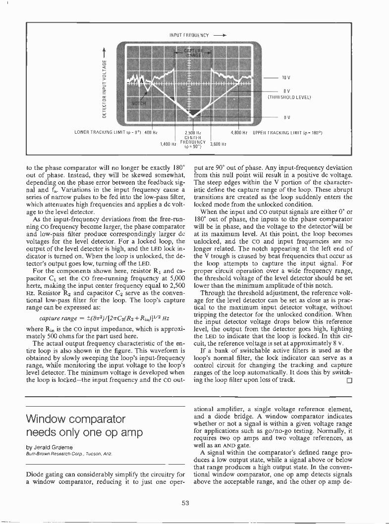
INPUT FREQUENCY -110-
1111111111111111111MIRS111111111110t,',11:111 NI1111111111111r'NEM
LOWER TRACKING LIMIT (0 = 0°) 400 Hz 2,500 HzCENTER
1,400 Hz FREQUENCY(0= 90°)
3,600 Hz
10 V
8V(THRESHOLD LEVEL)
0 V
4,800 Hz UPPER TRACKING LIMIT (0= 180°)
to the phase comparator will no longer be exactly 180°out of phase. Instead, they will be skewed somewhat,depending on the phase error between the feedback sig-nal and fn. Variations in the input frequency cause aseries of narrow pulses to be fed into the low-pass filter,which attenuates high frequencies and applies a dc volt-age to the level detector.
As the input -frequency deviations from the free -run-ning CO frequency become larger, the phase comparatorand low-pass filter produce correspondingly larger dcvoltages for the level detector. For a locked loop, theoutput of the level detector is high, and the LED lock in-dicator is turned on. When the loop is unlocked, the de-tector's output goes low, turning off the LED.
For the components shown here, resistor R1 and ca-pacitor C1 set the co free -running frequency at 5,000hertz, making the input center frequency equal to 2,500Hz. Resistor R2 and capacitor C2 serve as the conven-tional low-pass filter for the loop. The loop's capturerange can be expressed as:
±(872)/(27tC2(R2+Rin)1capture range = 1/2 Hz
where Rin is the co input impedance, which is approxi-mately 500 ohms for the part used here.
The actual output frequency characteristic of the en-tire loop is also shown in the figure. This waveform isobtained by slowly sweeping the loop's input -frequencyrange, while monitoring the input voltage to the loop'slevel detector. The minimum voltage is developed whenthe loop is locked-the input frequency and the co out-
put are 90° out of phase. Any input -frequency deviationfrom this null point will result in a positive dc voltage.The steep edges within the V portion of the character-istic define the capture range of the loop. These abrupttransitions are created as the loop suddenly enters thelocked mode from the unlocked condition.
When the input and co output signals are either 0° or180° out of phase, the inputs to the phase comparatorwill be in phase, and the voltage to the detector*will beat its maximum level. At this point, the loop becomesunlocked, and the co and input frequencies are nolonger related. The notch appearing at the left end ofthe V trough is caused by beat frequencies that occur asthe loop attempts to capture the input signal. Forproper circuit operation over a wide frequency range,the threshold voltage of the level detector should be setlower than the minimum amplitude of this notch.
Through the threshold adjustment, the reference volt-age for the level detector can be set as close as is prac-tical to the maximum input detector voltage, withouttripping the detector for the unlocked condition. Whenthe input detector voltage drops below this referencelevel, the output from the detector goes high, lightingthe LED to indicate that the loop is locked. In this cir-cuit, the reference voltage is set at approximately 8 v.
If a bank of switchable active filters is used as theloop's normal filter, the lock indicator can serve as acontrol circuit for changing the tracking and captureranges of the loop automatically. It does this by switch-ing the loop filter upon loss of track.
Window comparatorneeds only one op ampby Jerald GraemeBurr -Brown Research Corp., Tucson, Ariz.
Diode gating can considerably simplify the circuitry fora window comparator, reducing it to just one oper-
ational amplifier, a single voltage reference element,and a diode bridge. A window comparator indicateswhether or not a signal is within a given voltage rangefor applications such as go/no-go testing. Normally, itrequires two op amps and two voltage references, aswell as an AND gate.
A signal within the comparator's defined range pro-duces a low output state, while a signal above or belowthat range produces a high output state. In the conven-tional window comparator, one op amp detects signalsabove the acceptable range, and the other op amp de -
53
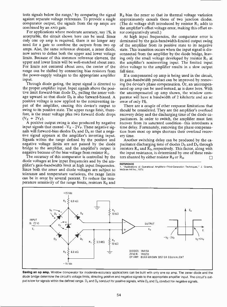
tects signals below the range,' by comparing the signalagainst separate voltage references. To provide a singlecomparator output, the signals from the op amps arecombined by an AND gate.
For applications where moderate accuracy, say 1%, isacceptable, the circuit shown here can be used. Sinceonly one op amp is required, there is no longer anyneed for a gate to combine the outputs from two opamps. Also, the same reference element, a zener diode,now serves to define both the upper and lower voltagelimits. Because of this common reference element, theupper and lower limits will be well -matched about zero.For limits not centered about zero, the center of therange can be shifted by connecting bias resistors fromthe power -supply voltages to the appropriate amplifierinput.
Through diode gating, the input signal is directed tothe proper amplifier input. Input signals above the posi-tive limit forward -bias diode D1, pulling the zener volt-age upward so that diode D2 is also forward -biased. Apositive voltage is now applied to the noninverting in-put of the amplifier, causing this device's output toswing to its positive state. The upper range limit, there-fore, is the zener voltage plus two forward diode drops(Vz + 2VF).
A positive output swing is also produced by negativeinput signals that exceed -Vz - 2VF. These negative sig-nals will forward -bias diodes D3 and D4 so that a nega-tive signal appears at the amplifier's inverting input.Signals within the range defined by the positive andnegative voltage limits are not passed by the diodebridge to the amplifier, and the amplifier's output isnegative because of the bias voltage from resistor R1.
The accuracy of this comparator is controlled by thediode voltages at low input frequencies and by the am-plifier's gain -bandwidth limit at high input frequencies.Since both the zener and diode voltages are subject totolerance and temperature variations, the range limitscan be in error by several percent. To reduce the tem-perature sensitivity of the range limits, resistors R2 and
R3 bias the zener so that its thermal voltage variationapproximately cancels those of two junction diodes.(The dc voltage shift introduced by resistor R1 adds tothe amplifier's offset voltage error, making this offset er-ror comparatively small.)
At high input frequencies, the comparator error isdominated by the gain -bandwidth -limited output swingof the amplifier from its positive state to its negativestate. This transition occurs when the input signal is dis-connected from the amplifier by the diode bridge, leav-ing only the small voltage developed by resistor R1 atthe amplifier's noninverting input. The limited inputdrive voltage to the amplifier results in a slow outputfall time.
If a compensated op amp is being used in the circuit,its gain -bandwidth product can be improved by remov-ing the device's phase compensation. Or, an uncompen-sated op amp can be used instead, as is done here. Withthe uncompensated op amp shown, the window com-parator will have a bandwidth of 2 kilohertz and an acerror of only 1%.
There are a couple of other response limitations thatshould be considered. They are the amplifier's overloadrecovery delay and the discharging time of the diode ca-pacitances. In order to switch, the amplifier must firstrecover from its saturated condition-this introduces atime delay. Fortunately, removing the phase compensa-tion from most op amps shortens their overload recov-ery time.
Another switching delay can be produced by the ca-pacitance discharging time of diodes D2 and D4 throughresistors R4 and R5, respectively. This factor, along withthe input resistance, is determined by one of these resis-tors shunted by either resistor R2 or R3.
REFERENCE1. "Applications of Operational Amplifiers-Third-Generation Techniques:. J. Graeme,McGraw-Hill Inc., 1973.
INPUT
(6-13 V)
Ei
D3
+15 Vdc
-15 Vdc
OUTPUT
Eo
-Vz -2VF
DIOOES: 1N4154ZENER: 1N5233OP AMP: BURR -BROWN 3057 OR EQUIVALENT
E.
Vz +2VF
Saving an op amp. Window comparator for moderate -accuracy applications can be built with only one op amp. The zener diode and thediode bridge determine the circuit's voltage limits, directing positive and negative signals to the appropriate amplifier input. The circuit's out-put is low for signals within the defined range. D1 and D2 conduct for positive signals, while D3 and D4 conduct for negative signals.
54
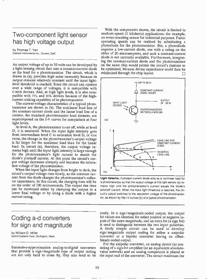
Two -component light sensorhas high voltage outputby Thomas T. YenStatham Instruments Inc., Oxnard, Calif.
An output voltage of up to 50 volts can be developed bya light -sensing circuit that uses a constant -current diodeas the load for a phototransistor. The circuit, which isdrawn in (a), provides high noise immunity because itsoutput remains relatively constant until the input light -level threshold is reached. Since the circuit can operateover a wide range of voltages, it is compatible withc-mos devices. And, at high light levels, it is also com-patible with rrL and DTL devices because of the high-current -sinking capability of its phototransistor.
The current -voltage characteristics of a typical photo-transistor are shown in (b). The nonlinear load line ofthe constant -current diode and the linear load line of aresistor, the standard phototransistor load element, aresuperimposed on the I -V curves for comparison at fourlight levels.
At level A, the phototransistor is cut off, while at levelD, it is saturated. When the input light intensity goesfrom intermediate level C to saturation level D, or viceversa, the change in the phototransistor's output voltageis far larger for the nonlinear load than for the linearload. In circuit (a), therefore, the output voltage re-mains high until the input light intensity is large enoughfor the phototransistor's light current to match thediode's pinchoff current. At this point the circuit's out-put voltage decreases abruptly and becomes the satura-tion voltage of the phototransistor.
When the input light changes from bright to dark, thecircuit's output voltage rises slowly, as the constant cur-rent from the diode charges the phototransistor's collec-tor capacitance. In this circuit, the charging time will beon the order of 100 microseconds. The output rise timecan be shortened either by clamping the output to alower final voltage or by using a diode with a highercurrent rating.
With the components shown, the circuit is limited tomedium -speed (1 kilohertz) applications-for example,an event -counting sensor for industrial purposes. Fasteroperating speeds can be realized by substituting aphotodiode for the phototransistor. But, a photodioderequires a low -current diode, one with a rating on theorder of 20 microamperes, and such a constant -currentdiode is not currently available. Furthermore, integrat-ing the constant -current diode and the phototransistoron the same chip would permit the circuit's risetime tobe optimized, because device capacitance could then beminimized through the chip layout. 0
(a)
lb)
INPUT LIGHTSOURCE
+V (UP TO 50 VI
CONSTANT -CURRENTDIODE 1N5283
OUTPUT(0- 50 VI
PHOTOTRANSISTORMOTOROLA MRD300
LOAD LINE FORCONSTANT CURRENTDIODE
LOADRESISTIVELINEB
VSATA V
Light detctor. Constant -current diode acts as a nonlinear load fora phototransistor so that the output voltage of this light sensor (a) re-mains high until the phototransistor's current equals the diode'spinchoff current. When the input light threshold is reached, the cir-cuit's output switches to the saturation voltage of the phototransis-tor, as shown by the I -V curves (b) of a typical phototransistor.
Coding a -d convertersfor sign and magnitudeby William D. MillerHybrid Systems Corp., Burlington, Mass.
Successive -approximation analog -to -digital convertersthat provide a sign/magnitude type of output codingare not only hard to come by, they also tend to be
costly. In a sign/magnitude-coded output, the outputbit values are identical for either positive or negative in-puts of the same magnitude, and an extra bit (a sign bit)is used to distinguish between the two input polarities.A fairly simple circuit can be used to developsign/magnitude output coding for either a unipolarconverter or a bipolar converter having an offset -binary -coded output.
For the unipolar converter, an analog circuit (a) con-sisting of a sign -bit amplifier (or an equivalent absolute -
value network) and an analog comparator is placed atthe input end of the converter. The circuit maintains the
55
OBIPOLARANALOGINPUT
(a)
ANALOGCOMPARATOR
ET
L
SIGN BIT AMPLIFIER
IN
UNIPOLARA- D
CONVERTER
SIGN -BIT AMPLIFIER: HYBRID SYSTEMS A901 OR EQUIVALENT
MAGNITUDEBITS
SIGNf BIT
LEASTSIGNIFICANT LEAST SIGNIFICANT BIT
CoeBIT tiCO
C.M
BIPOLARA- D
CONVERTER
BOB
A,
B,
4 -BITMAGNITUDEBSIVI
(WITH FULLOFFSET BINARY A06 ADDER
ASCODING) A3
13,4 SIGNIFICANT BIT
h,
MOSTSOB
A4 } OVERFLOWMOSTSIGNIFICANT
SN7486BIT45V SN /483
(b)OB = OFFSET BINARYSM = SIGN/MAGNITUDE
unipolar input to the converter to preserve the magni-tude information, while the sign information is gener-ated on a separate line.
Besides accommodating any unipolar code, this ap-proach provides the zero -plus and zero -minus codesthat occur within ±1/2 least significant bit of the true zeroinput. Parts cost for the circuit, however, is rather high-in the range of $30.
A more economical digital approach (b) can be usedif the a -d converter is one of the readily available bipo-lar types having an offset -binary-coded output. Exclu-sive -OR gates and full adders are the logic elementsneeded to convert from the offset binary code to thesign/magnitude code. With this technique, parts cost isonly $5 or so for a 12 -bit converter.
The figure shows a representative four -bit system.The table compares the offset binary and sign/magnitude codes for the 16 corresponding digital out-put words. For words 1 through 8, each bit in each codeis identical. For words 9 through 16, one code is thetwo's complement of the other code. For clarity, themost significant bit of each code is assumed to be thesame for the same word.
For words 9 through 16, the exclusive -OR gates trans-late the offset -binary-coded output bits from the con-verter to a one's complement code. These gates also de-velop the carry -in bit for the four -bit adder. Three of
Ssm SIGN
CODE CONVERSION
FROMOFFSET BINARY
TOSIGN/MAGNITUDE
WORD Boll A08 BOB COB SS NI Asm BSM CS AI
1
2
3
4
5
6
7
8
9
10
11
12
13
14
15
16
0
0
0
0
0
0
0
0
1 1
1 1
1
1
0 1
0 1
o o
O 0
1 1
1 1
1
1
0 1
0 1
o o
0 0
0
0
0
0
0
0
0
0
SIGN MAGNITUDE
1 1
1 1
1 1
1 1
1
1
1
1
o o
0
o o
1
0 1
0 1
1
1
0 0
1 1
1
0 1
0 0
1
1 1
0
0 0
1
1 1
4- OVERFLOW AT `4 +
SIGN MAGNITUDE
Simple conversion. Analog circuit o (a) enables a unipolar a -dconverter to accept bipolar inputs and produce a sign/magnitude-coded output. A sign -bit amplifier or an equivalent absolute -valuenetwork performs the polarity selection. The digital circuit of (b)translates the offset -binary-coded output of a bipolar a -d converterto a sign/magnitude-coded output. A four -bit system is shown here.
56

the adder's output sums provide the sign/magnitudedata in the desired two's complement code. The adder'sfourth output sum acts as an overflow bit to indicatewhen the input count exceeds the adder's capacity.
Circuit (b) produces a single nonpolarized output
word of 1000 when the analog input is within -±.1/2 leastsignificant bit. Therefore, this circuit is suitable for ap-plications requiring mirror symmetry between corre-sponding nonzero positive and negative words but notultrafine resolution about zero. 0
Getting extra control overoutput periods of IC timerby Arthur R. KlingerUnited States Air Force, Sheppard Air Force Base, Wichita Falls, Texas
The 555 -type IC timer, which is a versatile circuit build-ing block, becomes even more useful when its low andhigh output periods are controlled fully. The two cir-cuits shown here, for example, enable the designer tohave full -range, completely independent control overthe timer's output periods, or, conversely, to make theperiods fully dependent so that the output duty cyclecan be varied easily over a wide range while keepingoutput pulse rate constant.
Circuit (a) is for independent control over the peri-ods. Diodes D1 and D2 provide separate paths for thetiming capacitor's (C) charging and discharging cur-rents. Potentiometers R1 and R2 control the high andlow periods independently over the timer's completenormal range. Resistor R3 is included to provide thesame minimum fixed resistance in the discharge loop asresistor R4 provides in the charging loop.
When R1 = R3 and R2 = R4, a single calibrated dialcan be shared by potentiometers R1 and R2 (through aconcentric control). If R1 = R2 = 10 megohms andR3 = R4 = 1,000 ohms, the ratio of high -to -low or low -to -high periods can approach 10,000:1.
Circuit (b), which is only a slightly modified version
of circuit (a), makes the periods dependent. As poten-tiometer R1 is varied, one period is decreased while theother is increased proportionately. If R1 = 10 megohmsand R2 = R3 = 1,000 ohms, the timer's duty cycle willrange from about 0.01% to 99.99%, with little change inthe output pulse frequency.
In both circuits, the voltage drop across the diodesdecreases the effective voltage across the RC timing net-work, so that the output periods will be smaller thanthey usually are. Normally, the timer's high output pe-riod can be described by:
TH1 = RC ln[(Vcc - Vi)/(Vcc - V2)]
where R is the total resistance in series with timing ca-pacitor C, Vcc is the supply voltage, VI is the low trig-ger threshold, and V2 is the high trigger threshold.
For these circuits, however, the constant voltage dropacross the diodes must be accounted for. If each diodedrop is approximately 0.6 volt, then:
THI = RC InV(Vcc -0.6)- Vi) ((Vcc - 0.6) - V2)]
The lower the supply voltage, then, the greater is the ef-fect of the diode drop. When the timer is operated in itsastable mode, the period is roughly 0.76RC for a 15-vsupply, and for astable operation with 5-v supply, theperiod is about 1.4RC. This means that the timer's out-put periods will be more sensitive to variations in thepower -supply voltage, which may be a disadvantage insome applications.
Vcc(a)
(HIGH/LOWPERIOD RATIO
10,000:1)
01, 02: 1N914
(b)
OUTPUT
(DUTYCYCLERANGE
0.01% - 99.99%)
Simple but effective. When a pair of diodes is used to separate the charging and discharging paths of an IC timer, the high and low outpu
periods of this device can be controlled easily. The periods can be made independent of each other, as in (a), or fully dependent withoutchanging the output pulse frequency, as in (b). The diode drops, however, make the timer more sensitive to supply variations.
57

Regulator for op ampspractically powers itselfby Richard EckhardtElectronics Consulting & Development, Cambridge, Mass.
Here's a rather novel way to build a dual -voltage regu-lator for powering operational amplifiers that offersgood tracking, as well as low ripple. Tracking betweenthe two output voltages is good because only one refer-ence source is used for both the positive and negativesides of the regulator. Although the circuit employs twoop amps itself, they are powered by their own outputs.Furthermore, the circuit's output -current capability ison the order of several amperes, and output ripple isheld to less than 1 millivolt peak -to -peak.
The circuit, shown in the figure, operates as a conven-tional series -pass regulator on its positive side to de-
velop its + 15 -volt output. Amplifier Ai is used for er-ror -detection. The pass transistor for the positive side isbiased on from the unregulated + 20-v input supplyvoltage. The output voltage from amplifier Ai then ad-justs this transistor's output.
On the negative side (-15-v output) of the regulator,amplifier A2 operates as a unity -gain follower. The passtransistor on the negative side is biased in a mannersimilar to its positive counterpart. The value of the bias-ing resistor for the negative pass transistor is differentfrom the value of the biasing resistor for the positivepass transistor in order to bring Az's output closer to thenegative supply voltage.
Since amplifier A2 is wired in a follower configura-tion, the reference voltage developed by the zener diodecan be used for both the positive and negative sides ofthe regulator. The two output voltages, therefore, trackeach other within approximately 50 my.
With suitable modification, the same circuit approachcan be used to build a regulator for devices other thanop amps that require a split supply.
+20 V
22 1d2
2N3712
2N3904
3.9 kS2
47pF
A, 741
v-
1 kS2
6.3 V
15 kit
VOLTAGEADJUST
5 kS2
47µF
10 k62
+15 V OUT
10 kl-2.
20 V
47µF
3.9 kS2
We
2N3906
2N3192
A2 741
4.7 kS2
41pF
10 k11
10 kS2
GNU
-15 V OUT
Split supply. Regulator circuit for op amps develops ±15-V outputs from a ±20-V unregulated source with less than 1 millivolt of ripple. Al-though the regulator uses op amps itself, they receive their power inputs from their own outputs. Ampflier A1 acts as an error detector, whileamplifier A2 is a voltage follower. The single zener voltage reference means that tracking is good between the positive and negative sides.
58

Analog filter can beprogramed digitallyby Leonard M. SmithlineLansing Research Corp., Ithaca, N. Y.
The frequency response of an analog active filter can beselected digitally, yet with the resolution and accuracyof resistive tuning and the dc stability of capacitive tun-ing. The filter accepts TTL inputs, permitting it to becontrolled directly by a computer and making it idealfor electronically switched systems. Furthermore, thisdigitally programable filter is cost -competitive with me-chanically switched types of filters, especially for high -order filter functions.
A simple first -order low-pass filter is drawn in (a).The corner frequency of this circuit is determined bythe proportion (a) of the amplifier output voltage (V)that is applied to the feedback capacitor (C). Since ap-plying a voltage of magnitude aV to capacitor C pro-duces the same feedback current as applying a voltageof magnitude V to capacitor aC, the value of capaci-tor C is effectively multiplied by a. Therefore, the fil-ter's corner frequency can be written as:
cab = 1 / aRiC
where R1 is the feedback resistor. The over-all dc gain ofthe circuit is unaffected by loop gain a.
The effective multiplication of capacitance C by gaina can be used to control the filter's corner frequency, asshown in (b). In this circuit, the filter's corner frequencyis determined by logic inputs through a voltage -dividersetup. Resistor R. is the upper leg of the divider, whilethe resistance of the lower leg is selected by enablingthe appropriate Tn. inverter buffer. When a logic inputturns on one of the buffers, the resistor associated withthat buffer is shorted to ground.
Resistor Rb provides the appropriate bias voltage forthe buffers. The transistor, which is wired as an emitter -
follower, reduces the resistance of the voltage dividerthat is reflected forward in series with capacitor C. ThisThevinin equivalent resistance (RT) is divided by thecurrent gain (/3) of the emitter -follower. For the circuitto operate properly:
RT/,6 must be much less than Rill Rf
where R1 is the input resistor. Since the dc levels of boththe buffers and the transistor are blocked by the capaci-tor, there is no need for any bias stabilization circuitry.
If the effects of biasing resistor Re are neglected, pro-gramable gain a can be expressed as:
a = 1/[1 + (12./Rb) + ER,Gi]
where G1 represents the conductance of those resistors,R1 through R. , whose buffers are enabled. The filter'scorner frequency now becomes:
wt. = 0-)0(K + ER.Gi)
where:
wa = 1 / RfCK = 1 + (Ra/Rb)
The filter's starting frequency-that is, the corner fre-quency of the filter with none of the logic buffers en-abled-is equal to Kwo. And each increment above thisfrequency, as each logic buffer is enabled, is equal towoRaGi. Since the effects of the enabled buffers are ad-ditive, the filter can be programed to accept either stan-dard binary codes or a binary -coded -decimal input. Forthe component values cited in the figure, c..). is 100 radi-ans/second, K is 2, the starting frequency is 200 rad/ s,and the frequency increment is 250 rad/s.
Moreover, the programing approach that is shownhere can be extended to higher -order filters through theuse of either the standard biquad or state -variable filterconfigurations.1,2
REFERENCES1. A.E. Schultz, "Active Filters Are Moving toward Standardization," Electronic Products,June 18, 1973.2. G.E. Tobey, J.G. Graeme, L.P. Huelsman, "Operational Amplifiers-Design and Appli-cations," McGraw-Hill Inc., 1971.
( a)
INPUT
OUTPUT
Logic -controlled frequency response. The corner frequency of thefirst -order low-pass filter of (a) can be varied by using loop gain tomultiply capacitance. In (b), this is done digitally through a voltage -divider arrangement. Logic buffers control the resistance of thelower leg of the divider, while the upper leg is formed by resistor R..When a buffer is enabled, its associated resistor is grounded.
( b )
INPUTRi
1001(2
134
500 SZ
0.1 µF
100 kS2
NATIONALLM 307
R2 RI
2 kS/ 4 kS2
\-- PROGRAMMING INPUTS
-15 V
+15 V
Rc
10 kit
OUTPUT
2N3906
59
Attenuating transientsin analog FET switchesby Leland ShaefferSiliconix Inc., Santa Clara, Gaht
Analog field -effect -transistor switches may be high-speed devices, but the faster they are toggled, thegreater is the risk of unwanted output switching tran-sients. The amplitude of these glitches or spikes can begreatly attentuated by synchronizing the toggling of oneFET switch with a second FET switch through logicpulses that have variable rise times and fixed fall times.
Undesirable spiking can occur at the output of ananalog switch during toggling because, inside the de-vice, charge can be coupled through either its gate -source or gate -drain capacitance. Previous attempts tocancel these glitches by applying out -of -phase spikesfrom a second switch failed because turn -on and turn-off times generally vary too much between devices.
In the circuit shown here, rrL inverters having open -collector outputs are used to develop the synchronizinglogic pulses. Since these inverters have a pull -down cur-rent that is an order of magnitude greater than theirpull-up current, the rise time of their output pulses canbe increased without appreciably affecting the fall timeof their output pulses. Fixed resistors (RL) establish thepull-up currents for the inverters.
The output rise times of the inverters determine thetimes required to reach the toggling thresholds ofanalog switches Si and S2. For the FET devices usedhere, this threshold is approximately 1.4 volts. Variablecapacitors (C1 and C2) at the outputs of the inverterspermit the rise times of these units to be set at the val-ues needed to synchronize switches Si and S2.
Now the turn -on of switch Si can be made to coincidewith the turn-off of switch S2, and the turn-off of Si canbe synchronized with the turn -on of S2. When theswitches are properly matched in this way, the tran-sients appearing at the output of Si can be reduced by afactor of 5 or more if RL is greater than or equal to10 kilohms and C1 and C2 are about 12 picofarads. ForRL = 75 ohms, the magnitude of the unwanted tran-sients will at least be halved.
Transient attenuation can be improved still furtherby connecting a zener diode (a 6.8-y device, in this ex-ample) shunted with a bypass capacitor in series withthe negative power supply. The glitches will then be re-duced by an additional factor of 2 for both RL = 75ohms and RL = 10 kilohms. However, the analog out-put voltage swing, which is normally + 15 v to -7.5 v,will now be limited to +15 v and -1/2 v.
To adjust the circuit properly, first set capacitor C3 atits minimum value and adjust capacitor C1 for a min-imum turn-off transient. The value of capacitor C3 isthen increased until maximum transient cancellation isobtained. Next, capacitor C2 is adjusted for a minimumturn -on transient. Capacitors C1 and C2 will interactslightly with each other, and some compromise may benecessary in the adjustment of C3 for minimum turn -onand turn-off transients.
In the circuit drawn in the figure, only one signalsource is used, and switches Si and S2 provide single -pole, single -throw switching action. To accommodate asecond signal source and obtain single -pole, double -throw action, the drain of Si is connected directly (with-out capacitor C3) to the drain of S2. The second signalsource is then applied to the source terminal of switchS2. When the switches are wired in this manner, themake -before -break interval is about 30 nanoseconds.
LOGICIN
+5 V
2 k,S1.
4.5 - 50pF
RL
2 k1-2
INVERTERS: 7405
ANALOG SWITCH: SILICONIX 0 0181
2 kS2
+15 V
4.5 - 50µF
VL
a
VccSOURCE
-
DRAIN
VE ESOURCE
-15 V
jr4.5 - 50µF
5)SIGNALIN
SIGNALO OUT
Squelching spikes. Switching transients at the output of an analog FET switch can be greatly attenuated by synchronizing the turn -on andturn-off of one switch with those of a second switch. Open -collector TTL inverters produce logic pulses whose output rise times can be variedwhile their output fall times remain fixed. The turn -on of switch S1 is made to coincide with the turn-off of switch S2, and viceversa.
60
Coherent phase modulationattains data rates of 100 MHzby Roland J. TurnerGeneral Electric Co., Space Division, King of Prussia, Pa.
Though phase -modulation schemes have till now beenlimited to modulation rates at video frequencies of 5megahertz or less, a new technique permits 100- to 200 -wiz data rates. The key is an ordinary step -recovery
diode that produces a three -level phase code by thesimple means of varying the reflection coefficient of thetransmission line.
In the modulation setup shown in the figure, the shortair line is terminated with an rf diode, whose state de-termines the reflection coefficient of the transmissionline. The state of this terminating diode is establishedby its drive current. A type 1N914 device is used here,but a hot -carrier or p-i-n diode could be used instead.
The step -recovery diode generates an impulse func-tion each time the input rf sine wave passes throughzero in the negative -going direction. This impulse func-tion, which occurs at the input rf bit rate, establishes the
rf BIT RATEGENERATOR
BROADBAND TRANSFORMER:VARI-L 50 - 50B, 50 12/50 52
TRANSMISSION LINESTEP -RECOVERY1 S4Y04LV12A1NIA
DIODE
LOAD
5052
AIRLINE: 10 - 30 cm, 50 12
- =
+V \ /SIN,
I (CURRENTSOURCE)
100 pF
TERMINATING DIODE1N914
1RECEIVER
MODULATION OUTPUT PHASE SPECTRUM FREQUENCY SPECTRUM
NONE(REFERENCE0° PHASE)
tr/2
37/2
0t ttt
Flo))
0 L 6r/T
27r/T
LOGIC 0(90°PHASESHIFT)
it/2
3ir/2
0 W
LOGIC I(180° PHASESHIFT)
-.I A 14-
77
7712
37r/2
0
Hu))
/27r/A
o
2-fr/T
W
High-speed transmission. Data can be transmitted at rf rates of 100 to 200 megahertz with this coherent -phase -modulation schemeA three -level phase code is set up by changing the reflection coefficient of the transmission line by means of the terminating diode at the end
of the air line. The step -recovery diode acts as a waveform generator, producing impulse, doublet, and square -wave functions.
61

setup's reference phase (no modulation). For this case,the transmission line is terminated in its characteristicimpedance, and there is no reflection. Therefore, thereference phase is represented by a 0° phase shift.
As the sine -wave drive signal reverse -biases the step-recovery diode, this device's capacitance drops radi-cally. However, because of the minority -charge storagein the diode, the current charge is not neutralizedquickly, and it forces the voltage across the diode to risevery rapidly. The result is an impulse function that lastsonly 1 to 2 nanoseconds.
When there is a logic 0 at the end of the air line, thisline is terminated in an impedance that's low in relationto the characteristic impedance of the transmission line.The reflection coefficient now is -1, and a doublet wave-form is produced at the step -recovery diode. The phasedifference between the impulse and doublet waveformsis 90°.
When there is a logic 1 at the end of the air line, thisline is terminated in a high impedance with respect tothe characteristic impedance of the transmission line.The reflection coefficient becomes + 1, and the step -re-covery diode generates a double -width square wave,which is 180° out of phase with the reference impulsefunction.
The three waveforms form a flat comb spectrum withcoherent phase modulation on all spectral lines. Thismeans that the phase from one spectral line to the next
remains the same. The coherent phase modulation canbe used to represent a three -level code in the phasedomain.
The 0° phase, which is represented by the impulsefunction, can be used in a passive receiver to demodu-late the other two discrete phases-the 90° and 180°shifts produced by the doublet and square -wave func-tions. These latter two phases can then represent abinary code in the phase domain that provides coherentphase modulation on all spectral lines of the comb spec-trum. For an rf bit rate of 100 MHz, a spectral line willoccur at multiples of 100 MHz, up to about 1 gigahertz.
With this type of phase coding, data can be trans-mitted at half the rf bit rate. For example, if the basic rfbit rate is 100 MHz, information can be transmitted at50 million bits per second. Additionally, the redundantcoherent reception on the many spectral lines makes thereceiver immune to Johnson or man -generated noise.
The modulation scheme can also be used for a broad-band rf impulse noise jammer by modulating the cur-rent of the terminating diode with white video noise.Or, it can be the basis for an rf test function generatorfor evaluating the transient response of communicationsubsystems to complex excitation.
The output amplitude of the modulation circuit is1 volt peak into 50 ohms for the impulse and square-wave functions and 2 v, peak to peak, into 50 ohms foithe doublet function.
Single switch regulatesnumber of pulsesby Mahesh BhutaIBM Corp., General Products division, San Jose, Calif.
A simple SCR ring counter or a serial-in/parallel-outshift register will make a pulse generator produce apredetermined number of pulses at the activation of asingle switch. The number of pulses generated dependson which switch is closed. A pulse frequency of 100kilohertz is easily attainable.
Circuit (a), which contains the SCR ring counter, em-ploys a conventional astable multivibrator as its basicpulse source. Transistors Q1 and Q2 make up this multi -vibrator. When any one of the switches is closed, tran-sistor Qi turns on, triggering the astable.
The astable includes an SCR so that transistor Q2 willalways saturate before transistor Qi. When Q2 gener-ates the first output pulse, the rising edge of this initialpulse fires SCRA, enabling the astable to operate in itsfree -running mode. Bleeder resistor RB provides theholding current for SCRA.
The output from transistor Q3 is fed to the SCR ringcounter. Capacitors C, diodes D, and resistors R formthe steering circuit that enables the appropriate pulsefrom Q3 to fire the appropriate number of SCRs. If k
pulses are desired, the kth switch is activated, theastable will generate k pulses, and the kth pulse will firethe kth SCR, making its anode go to 0.3 volt. This imme-diately deprives transistor Qi of its base drive, and theastable is turned off.
When the kth switch is released, the power to the SCRcounter is removed, and the SCRs are switched off. Thecounter is automatically reset so that it is ready to gen-erate the next desired set of pulses.
The SCR counter can be replaced with a serial-in/parallel-out shift register, as shown in (b). The regis-ter's SERIAL inputs are tied high. When the switches arein their normally closed positions, the register's CLEARinput and all its outputs are low.
Transistors Qi and Q2 are connected as an astablemultivibrator. When any one of the switches is acti-vated, transistor Qi turns on. The rising edge of the firstpulse from transistor Q2 will trigger the SCR, which willstay on because of bleeder resistor RB.
The output pulses from the astable provide the clocksignal for the shift register. Each pulse advances the reg-ister until the kth output-the one that is connected tothe base of transistor Q1 through the kth switch-goeshigh. Once this happens, the astable switches off. Whenthe kth switch is released, the register's CLEAR inputgoes low, and the shift register is automatically reset.The next set of pulses can now be generated.
62
(a)
S S2
4117111
0 0
1 kf2
0.001µF
CI
R2
S3 Jo s,
I I
SC 04
0*
- C-10.001pF I0.001 pF -1.0.001pF -1-0.001pF
2N4403
0.001pF
2N4401
0.001pF
0.001pF
22 kS2
250 pF
SCRs: MOTOROLA MCR102 R, 22 kS2
DIODES: 1N461 R21 2 kS2
VCC
C12
2N4403
OUTPUT
( b)
OUTPUT
SHIFT REGISTER:NATIONAL SEMICONDUCTOR MM74C164
+5 V
CLOCK
SERIAL IN CLK CLK CLK CLK CLK CLK CLK CLK
0 0 0
I 111
SERIAL IN CLR CLR CLR CLR
CLEAR
7 V V
2k12
10 k12
2N4403
2N4401
1 kS2
+5 V
2N4403
3.9 kS2
A- 22 kS2
0.001pF
0.001 pF2N4401
MOTOROLAMCR 102
250 pF
1 kS2
SiO
2 kS2
SCR
0S
2
R B
1 kg -2,
Controlled pulse burst. With either one of these circuits, the desired
number of pulses can be generated by activating a single switch.Both circuits employ an astable multivibrator as the basic pulsesource. To produce k pulses, the kth switch is activated. In circuit(a), an SCR ring counter is used to log the pulses, while circuit (b)uses a serial-in/parallel-out shift register instead.
63

Analog gate and zener diodegive 70 -dB isolation at 80 MHzby Roland J. TurnerGeneral Electric Co., King of Prussia, Pa.
When conventional double -balanced Schottky diodemixers are used as analog signal gates, they have twoserious limitations: the "ofr impedance of a seriesdiode offers a switch isolation of less than 40 decibels,and the peak radio -frequency input signal cannot ex-ceed the series diode's forward blocking voltage -500millivolts at room temperature, but falling to 300 my athigher temperatures. An rf analog gate with both largersignal -handling capability and higher "off" isolationwould be very useful, for example, in a pair of switchescontrolling a transmitter and receiver that share a com-mon antenna.
The analog gate shown in the diagram achieves an"off' isolation of as much as 70 dB at 80 megahertzwithout using matched diodes. When +30 milliamperesis supplied to the gate, it turns on shunt diodes D1 and
D2, while the series diodes D3 and D4 are reverse -biasedby a voltage equal to the zener voltage at D5 minus thepositive swing of the input signal. With the gate biasedoff in this way, variable capacitor C1 is trimmed, so thatout -of -phase signals cancel signal leakage through thegate.
With a 6-v zener diode, this circuit isolates input sig-nals of as much as 10 v peak to peak-whereas themixer gate cannot handle even 1 v without letting thesignal break through.
On the other hand, when the current is -30 mA,diodes D3 and D4 are forward -biased and the shuntdiodes D1 and D2 become reverse -biased. The Schottkydiodes have a dynamic impedance of 10 ohms, which ismuch less than the typical antenna impedance as seenfrom this gate (about 200 ohms). Thus the input signalpasses through the gate with an insertion loss of lessthan 0.50 dB.
The gate's on -off status is controlled by the currentsource shown at the bottom of the.diagram. When thecontrol signal is at 12 v, the pnp transistor on the left isturned on, supplying + 60 mA-half to the gate to turnit off, and half to the npn current sink on the right. Butwhen the control signal rises to 15 v, the pnp transistoris cut off and the npn device, which stays on, reverses
SIGNALCONTROL
+15 V
+12 V
ALL SCHOTTKY DIODES: HP2305ZENER DIODE: 1N754 A OR B
+15 V -15 V
GATED RF OUT
--(1111-71111P-
2.4 Id2
High Isolation. Control signal (lower left) turns on pnp transistor, providing + 30 mA to gate circuit at top, to turn it off and block passage orf signal to antenna. When control is up, npn device takes over, drawing -30 mA from gate and turning it on. Zener voltage minus positiveswing of input signal establishes reverse bias on series diodes, achieving isolation of as much as 70 dB at 80 MHz.
64

the current passing through the gate connection.Both input and output transformers are conventional
components, with bifilar 1:1:1 windings on IndianaGeneral Q-3 core material. The center tap of the inputtransformer is grounded, while that of the output is
split. At this point an RC network collects the -30-mAcurrent when the gate is on. Because the two shuntdiodes may have different voltage drops, the resistanceis a potentiometer that can be adjusted to eliminate anydc bias at the output.
Single op amp comparesbipolar voltage magnitudesby F.N. Trofimenkoff and R.E. SmallwoodUniversity of Calgary, Alta., Canada
The operational -amplifier bridge circuit shown in Fig. 1is a window comparator for bipolar signals. It indicateswhen the magnitude of the input signal exceeds a presetvalue. Selection of resistor values sets positive and nega-tive trigger levels independently, so that the trip levelsfor the two polarities need not be the same.
To analyze the circuit, first ignore the output clamp-ing diode. The input diodes isolate one of the two signalpaths, depending on the polarity of ei. For e, positive:
ec, = -(e,- ed)(R2/ RI) - er(R2/ R3)
where ed is the voltage drop across the diode when itconducts. For e, negative:
eo[1 + (R2/R3)+ (R2/ R6)]
= (e1+ ed) - er(R2/ R3)[1+ (R4/R5)]
The switch -over points are defined by setting e. = 0 ineach of these expressions. For e, positive:
(e, - ed) = er(Ri/R3)
and for e, negative:-er[1 +(RI/ROI
(e,+ ed) -[1
, ,
4- (A3/ V 4" (A3/ It6)1
(1)
(2)
1. Comparator. Amplifier output is low when the input is betweentwo levels set by choice of resistances, and high when outside these
levels. The two trigger levels are independent.
If the positive and negative trip levels must have thesame magnitude, then the coefficients of er in equations(1) and (2) are equal. The equality reduces to:
[1 + (R3/R2) +.(R3/R6)] = [1 + (R4/R5)](R3/Ri) (3)
If the switching levels are different, equations (1) and(2) must be used to determine the resistor ratios. But re-gardless of the levels, R2 is very large and may even beinfinite-that is, the circuit may have an open -loop con-figuration-to provide the maximum gain and therebyproduce a sharp transition between the output states atthe switch -over points.
The circuit may be simplified if, for example, the ref-erence voltage is greater than the desired switch -overpoint. In that case, R4 = 0. If it is less, then R6 isomitted from the circuit. For symmetrical switching,making R4 + R5 approximately the same as R1 equal-izes the diode currents, thus more nearly matching thediode forward voltage drops.
If now the output clamp is taken into account, itkeeps the lower level of the output from going morethan very slightly negative, as shown in Fig. 2. The com-plement of this transfer function is obtained by chang-ing the polarities of the input diodes and the referencevoltage.
As a design example, suppose ±-10.0-volt switch -overpoints are required, and er = 15 v. Assume ed = 0.5 v,and use 11 kilohms fOr R1 and an open circuit for R2.Equations (1) and (3) show that R3 = 17.4 kilohms, R4= 0, R5 = 11 kilohms, and R6 = 29.9 kilohms. Build-ing the circuit with these- component values results inmeasured switch -over points of -10.12 and + 10.15 v.The actual switching is completed during a change in
2. Transfer function. Output clamp keeps low level only a fraction ofa volt below ground. The complementary function is obtainable byinverting the two input diodes and the reference voltage.
65

the input of less than a millivolt, because the amplifiergain is high and the open -loop configuration is used.
This simple circuit has some disadvantages. Amongthese are the forward voltage drops of the input diodes,which are significant. Consequently, the circuit cannotbe operated near e, = 0. These voltage drops can beminimized with germanium or hot -carrier diodes.
Another disadvantage is that the switch-over pointsare temperature -sensitive, because the diode forwarddrops have a temperature coefficient. Finally, the speedof the circuit depends on the type of operational ampli-fier and on the clamping scheme. Using a comparator inplace of the operational amplifier permits somewhatfaster switching. 0
Regulating voltage with justone quad IC and one supplyby R. A. KoehlerYork University, Toronto, Canada
Full -range, high-performance power supplies are oftenbulky and expensive because they require two indepen-dent voltage sources-one main and one reference-withassociated rectifiers, filter capacitors, and referenceregulator circuitry.
But only one unregulated source of about 26 volts dcand one ground -sensing quad operational amplifier arenecessary in a regulated power supply that provides 1ampere at 0 to 20 v with foldback current -limiting andoverload indication. It achieves line and load regulationwithin ±0.02% over the full range of load conditions,even when the input voltage varies between 24 and 28 vdc. When the regulator is quiescent, its current require-
ment amounts to less than 10 milliamperes.Amplifier Ai is a self -biased, constant -current ampli-
fier that provides a stable reference voltage [Electronics,March 13, 1972, p. 74]. Its output, Vi, depends on thebreakdown voltage Vz of the zener diode, Di:
V1 = 1/41 + (R1/R2)]
It is approximately 9.1 v for the values shown in thediagram. The potentiometers R3 and R4 bring V1 downto a desired value V2, which is amplified by A2 and theDarlington output stage to the output level:
Vout = V2(R5 + R6)/R6
With R4 at its maximum -voltage position, variable re-sistor R3 sets the voltage at exactly 20 v; thereafter, R4varies the output voltage over its full range. The outputstage gain is 2.5 for the values shown.
Amplifier A3 monitors the regulator's output cur-rent under varying loads. It compares the voltageacross R7 (a very small resistance) with the dropacross diode D2. Whenever the former is greater thanthe latter, the output of A3 drops, biasing diode D3 for-
24 - 28 VdcUNREGULATED
2 kS2Wt.
D,
RI R2
4 7 kS2. 10 k12
4.7 kS2
dAmeOVERLOADINDICATOR
A4
R3 62 kS2---5 k11
R4 "1-*10 kS2
22 kS2
2N3053
3.9k12
D3 y_ 10 k
2N3055
47
18 kS2
100 1(2
2
0.47 S2
-Now-do1 kS-2
R5
Ye%
150
4.7 IcS1
0- 20 V at 1 AREGULATED±0.02%
Ai TO A4: LM324N QUAD AMPLIFIERDi: 1N5234D2, D3: 1N4148LED: MV 50542N3055 REQUIRES A HEAT SINK
Op amp regulator. An unregulated 26 -volt source becomes a 1 -ampere 0 -to -20-V supply regulated to within ±0.02% by a simple quad oper-ational amplifier. Input can vary between 24 V and 28 V, and quiescent current is less than 10 mA. A light -emitting diode gives an overloadindication, the level of which depends on the value of resistor 1,18. Single power Darlington can replace the two transistors.
66

ward; thus it reduces the output voltage by removingthe drive to the Darlington stage. If the load continuesto increase, the output of A3 becomes low enough to in-dicate, through amplifier A4, and a light -emitting diode,an overload condition. The circuit's overload threshold
may be changed, if desired, by changing the value of re-sistor R8.
The output transistors may be replaced by a singlepower Darlington, such as 2N6050, to reduce the pack-age count from three to two.
As clipper, IC comparatoris improved by feedbackby Arthur D. Delagrange,Naval Surface Weapons Center, Silver Spring, Md.
When used as clippers, modem integrated -circuit com-parators are generally limited by input offset, not gain.To assure that the output will switch in a conventionalcircuit (Fig. 1), the peak input voltage must be greaterthan the differential current offset multiplied by thebias resistor value and added to the differential voltageoffset.
A smaller peak input voltage can be used, however, ifdc negative feedback is added to the negative input atpin 3, as shown in Fig. 2. The input offset is effectivelyreduced by the gain of the comparator as the circuitseeks its own bias point, just as operational -amplifiercircuits do. The output is symmetrical, even for inputlevels near or below the comparator input offset.
Substituting a current -limiting diode for the pullupresistor further improves output symmetry. TheSchottky diode provides a charging path for the low-pass capacitor to minimize startup time. If startup timeis not a problem, the Schottky diode may be replacedby an ordinary diode or eliminated altogether. To pre-vent the ac signal from feeding back and reducing sensi-tivity, the feedback RC time constant must be an orderof magnitude longer than the signal period times thegain. A multiple -stage RC network cannot be used be-cause it would introduce additional phase shift thatmight cause the circuit to oscillate.
As shown, the circuit does not work well with an un-symmetrical rectangular pulse -train input. For this spe-cial case, the voltage divider ratio must be the same asthe input symmetry ratio. This technique can also beused to give an unsymmetrical output for a symmetricalinput (except square wave) if desired.
Input and output waveforms are shown in Fig. 3 for asine wave input at a frequency of 1 kilohertz and anamplitude of 100 microvolts root -mean -square. Sincethe difference between input and output levels is about90 dB, circuit arrangements that create parasitic mustbe carefully avoided. To obtain the waveforms of Fig. 3,a 50 -ohm source was used, the output was loaded onlyby an oscilloscope, and power came from a well -regu-lated supply with a 1-microfarad ceramic bypass capaci-tor at the comparator.
1. Conventional. Input offset limits the utility of the comparator when
used as a clipper; it won't work with very small signals.
2. Improvement. Adding dc negative feedback reduces input offsetproduces symmetrical output if input divider has 50:50 ratio.
3. Result In this trace, the horizontal scale is 200 microseconds perdivision. Vertical scales are 500 microvolts per division for input(top), and 5 volts per division for output.
67
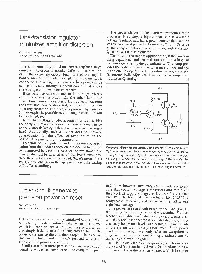
One -transistor regulatorminimizes amplifier distortionby Dale HilemanSphygmetrics Inc., Woodland Hills, Calif.
In a complementary -transistor power -amplifier stage,crossover distortion is usually difficult to control be-cause the extremely critical bias point of the stage ishard to maintain. But when a single bipolar transistor isconnected as a voltage regulator, the bias point can becontrolled easily through a potentiometer that allowsthe biasing conditions to be set exactly.
If the base bias current is too small, the stage exhibitssevere crossover distortion. On the other hand, toomuch bias causes a needlessly high collector current;the transistors can be damaged, or their lifetimes con-siderably shortened. If the stage is powered by batteries(for example, in portable equipment), battery life willbe shortened, too.
A resistive voltage divider is sometimes used to biasthe complementary transistors, but this scheme can beentirely unsatisfactory unless the bias source is regu-lated. Additionally, such a divider does not providecompensation for the effects of temperature on thebase -emitter junctions of the transistors.
To obtain better regulation and temperature compen-sation from the divider approach, a diode (or two) is of-ten connected between the bases of the two transistors.This diode must be selected carefully, since it must pro-duce the exact voltage drop needed. What's more, if thisvoltage drop changes as the equipment ages, the biasingwill suffer accordingly.
The circuit shown in the diagram overcomes theseproblems. It employs a bipolar transistor as a simplevoltage regulator and has a potentiometer that sets thestage's bias point precisely. Transistors Q1 and Q2 serveas the complementary power amplifier, with transistorQ3 acting as the bias regulator.
The input to the stage is applied through the two cou-pling capacitors, and the collector -emitter voltage oftransistor Q3 is set by the potentiometer. The setup pro-vides the optimum base bias for transistors Qi and Q2.If the circuit's operating temperature varies, transistorQ3 automatically adjusts the bias voltage to compensatetransistors Qi and Q2. 0
Crossover -distortion regulator. Complementary transistors 01 and02 form a power amplifier stage in which the bias point is controlled'closely through transistor 03 acting as a voltage regulator. The bias -adjusting potentiometer permits exact setting of the stage's biaspoint so that crossover distortion is held to a minimum. The transistorregulator also automatically compensates for varying temperature.
Timer circuit generatesprecision power -on resetby Jim FelpsTexas Instruments Inc., Austin, Texas
Digital systems are commonly initialized with a power-on reset, generated automatically when the powerswitch is turned on, but at no other time. A typical cir-cuit simply holds a reset line long enough for all thepower transients to die out, then drops it. Its durationisn't well defined, and it doesn't respond to dips orglitches in the primary power line.
Until recently, a more precise power -on reset circuitwould have been too complex and too costly to be justi-
fied. Now, however, new integrated circuits are avail-able that contain voltage comparators and referencesthat work at supply voltages as low as 4.5 volts. Onesuch IC is the National Semiconductor LM 3905' N-acomparator, reference, and precision timer all in oneeight -lead package.
In a power -on reset circuit based on the 3905 (Fig. 1),the timing begins only when the incoming V hasreached a suitable level, which can be very precisely es-tablished, and it is repeated if V, later drops even mo-mentarily below that level. As a result, all logic circuitsin the system are properly reset, even if the powerreaches its nominal level only after an exceptionallylong rise time, and no random logic failures can becaused by a power -line glitch.
IC 1 is a 3905 used as a comparator, which monitorsthe level of V (nominally 5 volts for transistor -transis-tor logic). It keeps the reset on whenever V is less than
68

SYSTEM CLOCK
VCC
5 k12
8
2
3
2 IcS2,
TRIGGER
LOGIC V
IC 1
VREF
3905
R/C
GND
4
5
3
TRIGGER
LOGIC V,
IC 2
VREF
3905
R/C
GND
4
22 4(12
VCC2
4
0PR
O
IC 3
7474
CL
6
POWER ON RESET
1. Reset generator. One comparator, one timer and a flip-flop join forces to produce a precisely timed power -on reset.
2. Sequence. When Ve, reaches a threshold defined by the setting ofthe 5-kilohm potentiometer, IC 1 turns on. Its rise is delayed by theRC network on IC 2. After one time constant, the clear input to IC 3is released, and the flip-flop is set by the next clock pulse.
4.75 V; its triggering level is established by setting Vee at4.75 and adjusting the 5-kilohm potentiometer at thepoint where the circuit's output (pin 5 of Ic 3) justswitches. Thereafter, when power is turned on and V,rises above this 4.75-v threshold (Fig. 2), ic 2, a 3905used as a timer, is released. One time constant later, asdetermined by the RC network connected to pins 2 and3 of Ic 2, an ordinary 7474 D -type flip-flop, ic 3, is re-leased. By this time the system clock should be runningsmoothly; at the next positive -going clock pulse the flip-flop is set, thus removing the power -on reset.
If the level of V drops below 4.75 v at any time,both timers and the flip-flop immediately go down, gen-erating another reset to the rest of the system. Restora-tion of V initiates the power -on sequence again.
If less precise reset timing is necessary, ic 2 may beomitted. The output of it 1 then rises as soon as thethreshold has been passed, and the flip-flop is set by thenext clock pulse. If several power supplies have to reachtheir nominal levels before the reset terminates, a sepa-rate 3095 as comparator can be connected to each sup-ply and all the outputs (pin 6) connected to each otheras a wired OR.
Generator's duty cyclestays constant under loadby Arthur R. KlingerSchool of Health Care Sciences, Sheppard AFB, Wichita Falls, Texas
In the 555 timer, configured as a square -wave gener-ator, adding one transistor and a diode to the,RC timingnetwork permits the frequency to be varied over a widerange while maintaining a constant 50% duty cycle [seealso Electronics, Sept. 19, p. 112].
In one simple configuration, a capacitor's charge anddischarge currents flow through only one resistor. The
Workhorse. This configuration of the 555 timer can drive a heavyload without distorting its square -wave output, even over a very wide
frequency range, unlike simpler hookups.
69
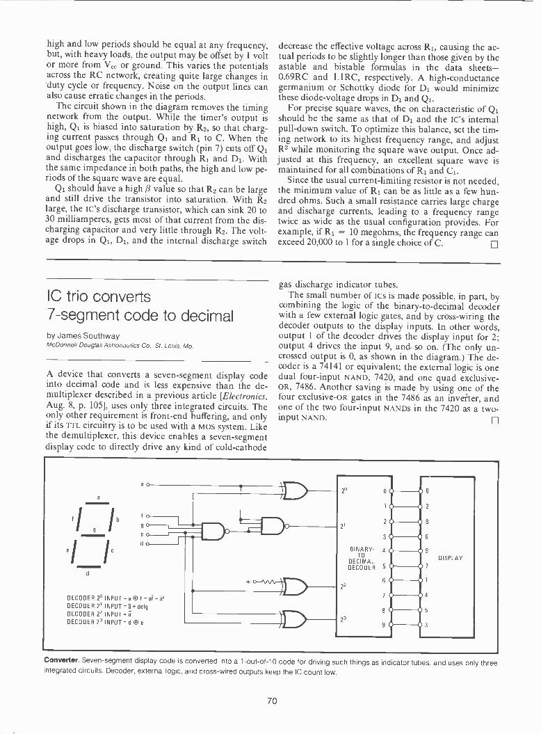
high and low periods should be equal at any frequency,but, with heavy loads, the output may be offset by 1 voltor more from Ve, or ground. This varies the potentialsacross the RC network, creating quite large changes induty cycle or frequency. Noise on the output lines canalso cause erratic changes in the periods.
The circuit shown in the diagram removes the timingnetwork from the output. While the timer's output ishigh, Qi is biased into saturation by R2, so that charg-ing current passes through Qi and R1 to C. When theoutput goes low, the discharge switch (pin 7) cuts off Qiand discharges the capacitor through R1 and Di. Withthe same impedance in both paths, the high and low pe-riods of the square wave are equal.
Qi should have a high )3 value so that R2 can be largeand still drive the transistor into saturation. With R2large, the ic's discharge transistor, which can sink 20 to30 milliamperes, gets most of that current from the dis-charging capacitor and very little through R2. The volt-age drops in Qi, D1, and the internal discharge switch
decrease the effective voltage across R1, causing the ac-tual periods to be slightly longer than those given by theastable and bistable formulas in the data sheets-0.69RC and 1.1RC, respectively. A high -conductancegermanium or Schottky diode for D1 would minimizethese diode -voltage drops in D1 and Q'.
For precise square waves, the on characteristic of Qishould be the same as that of D1 and the ic's internalpull -down switch. To optimize this balance, set the tim-ing network to its highest frequency range, and adjustR2 while monitoring the square wave output. Once ad-justed at this frequency, an excellent square wave ismaintained for all combinations of Ri and C1.
Since the usual current -limiting resistor is not needed,the minimum value of R1 can be as little as a few hun-dred ohms. Such a small resistance carries large chargeand discharge currents, leading to a frequency rangetwice as wide as the usual configuration provides. Forexample, if Ri = 10 megohms, the frequency range canexceed 20,000 to 1 for a single choice of C.
IC trio converts7 -segment code to decimalby James SouthwayMcDonnell Douglas Astronautics Co., St. Louis, Mo.
A device that converts a seven -segment display codeinto decimal code and is less expensive than the de -multiplexer described in a previous article [Electronics,Aug. 8, p. 105], uses only three integrated circuits. Theonly other requirement is front-end buffering, and onlyif its TIL circuitry is to be used with a mos system. Likethe demultiplexer, this device enables a seven -segmentdisplay code to directly drive any kind of cold -cathode
gas discharge indicator tubes.The small number of iCs is made possible, in part, by
combining the logic of the binary -to -decimal decoderwith a few external logic gates, and by cross -wiring thedecoder outputs to the display inputs. In other words,output 1 of the decoder drives the display input for 2;output 4 drives the input 9, and. so on. (The only un-crossed output is 0, as shown in the diagram.) The de-coder is a 74141 or equivalent; the external logic is onedual four -input NAND, 7420, and one quad exclusive-oR, 7486. Another saving is made by using one of thefour exclusive-oR gates in the 7486 as an inverter, andone of the two four -input NANDs in the 7420 as a two-input NAND.
a
d
ao
f o
d o -
DECODER 2° INPUT = a 0 I = af + ifDECODER 2' INPUT =5+ defgDECODER 22 INPUT =dDECODER 23 INPUT = d O e
me.
)D
000o-
1 0 0 2
2p 08
30 06BINARY- 4 0 9q
TO - DISPLAYDECIMALDECODER 0750
16 0 0
047 0
0580
90 03
Converter. Seven -segment display code is converted into a 1 -out -of -10 code for driving such things as indicator tubes, and uses only threeintegrated circuits. Decoder, external logic, and cross -wired outputs keep the IC count low.
70

Rectifying wide -range signalswith precision, variable gainby Jerald GraemeBurr -Brown Research Corp., Tucson. Anz
Millivolt -level signals cannot be rectified directly be-cause they are smaller than the typical 0.7 -volt dropacross a forward -biased diode. An operational amplifiercan reduce this loss to around 10 microvolts. But suchcircuits have a fixed gain when designed straight-forwardly, whereas variable gain is needed for rangecontrol in many applications-amplitude detection in acvoltmeters, for example.
Varying the gain has usually required either the ad-justment of more than one resistor or, in very complexcircuits, the use of a separate input amplifier. With theprecision rectifier shown in the diagram, however, vari-able gain is achieved without a gain -control amplifier.
Gain is controlled by a single variable resistor, whichcan be a potentiometer or a multiple -tap resistor. In ad-dition, this circuit has a high input impedance withoutan input buffer and requires only one resistance match.It has a gain range from unity to several thousand, forsignals from 1 millivolt to 10 v.
Rectification results when the feedback diodes areswitched by a reversal of the signal polarity, which inturn reverses the circuit gain polarity. With the diodesin one orientation, the signal path to the output is anoninverting amplifier; when they switch, it becomes avoltage follower and an inverting amplifier.
An input of positive signals produces a positive cur-rent i1 that turns diodes D2 and D3 on and D1 and D4off. This connects the noninverting amplifier Al to theoutput with a gain of 1/x, where x is a fraction repre-senting the potentiometer setting. In this mode A2 ismerely a ground return for the resistance xR1; its outputis disconnected from the circuit output by the reverse -biased diode D4. Thus the circuit output, controlled byAl alone, is e. = e,/x.
When the input signal swings negative, so does thecurrent i1. It switches off D2 and D3 and turns on D1and D4. Now the output of A2 is connected to the circuitoutput, and Al merely maintains a signal equal to el atits own inverting input. In doing so it also develops thissignal across the resistance xR1. That resistance acts asthe input resistor to A2, connected as an inverting am-plifier. With a gain of -1/x, this inverting amplifier de-velops e. = -e,/x, the negative of that produced bypositive signals. Since the polarity of the gain switcheswith that of the input signals, the output signal is alwayspositive, and e. = le,/xl.
Gain can be varied from unity to several thousand toaccommodate a wide range of signal levels. To insure
continually equal gain for positive and negative signals,it is only necessary to match the resistor R2 to the totalpotentiometer resistance R1. Op amp gain error directlyaffects circuit gain, but identically for both positive andnegative signals.
Otherwise, circuit accuracy depends upon the noises,dc errors, and ac responses of the op amps. Noise isn'tgenerally a major source of error in the practical signalrange of 1 my to 10 v, as long as the resistance levelsare low enough to limit the effects of noise currents atthe amplifier inputs.
Ideally, the diodes would switch just as the input sig-nal crosses zero, but the op amps' dc offset voltages-theinput levels below which the amplifiers produce no out-puts, as a result of mismatched transistors in the ampli-fiers-cause the circuit to depart from this ideal. The er-ror currents are:
(Vosi Vos2)/xl? + IHiand
(Vosi - V.,..2)/xR2 -1H2
This switching -point offset limits the circuit's operationwith very small signals. To extend it, the amplifiers arechosen for low bias currents, and the op -amp offset volt-ages are nulled. Matched op amps insure low initial dcerrors and thermal drifts.
Another output offset is produced by input currentsflowing through the feedback resistances. This offsetcannot be removed by the op -amp null controls withoutagain offsetting the diode switching, but it is minimized
Precision rectifier. Variable gain is achieved without a separategain -control amplifier, since the control potentiometer varies thegains of both amplifiers identically. Circuit gain ranges from unity toseveral thousand. Forward or reverse biasing of diodes make the cir-
cuit either an inverting or noninverting amplifier.
71
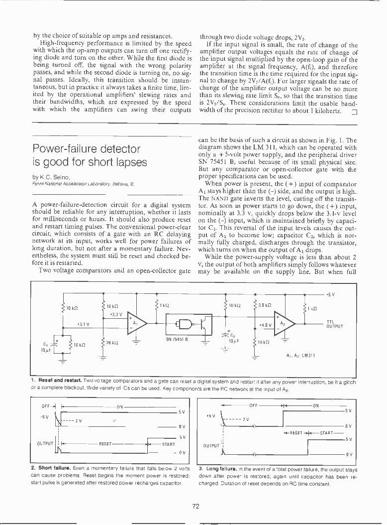
by the choice of suitable op amps and resistances.High -frequency performance is limited by the speed
with which the op -amp outputs can turn off one rectify-ing diode and turn on the other. While the first diode isbeing turned off, the signal with the wrong polaritypasses, and while the second diode is turning on, no sig-nal passes. Ideally, this transition should be instan-taneous, but in practice it always takes a finite time, lim-ited by the operational amplifiers' slewing rates andtheir bandwidths, which are expressed by the speedwith which the amplifiers can swing their outputs
through two diode voltage drops, 2V1.If the input signal is small, the rate of change of the
amplifier output voltages equals the rate of change ofthe input signal multiplied by the open -loop gain of theamplifier at the signal frequency, A(fi), and thereforethe transition time is the time required for the input sig-nal to change by 2Vf/A(fi). For larger signals the rate ofchange of the amplifier output voltage can be no morethan its slewing rate limit Sr, so that the transition timeis 2Vf/Sr. These considerations limit the usable band-width of the precision rectifier to about 1 kilohertz. p
Power -failure detectoris good for short lapsesby K.C. Seino,Fermi National Accelerator Laboratory, Batavia, Ill.
A power -failure -detection circuit for a digital systemshould be reliable for any interruption, whether it lastsfor milliseconds or hours. It should also produce resetand restart timing pulses. The conventional power -clearcircuit, which consists of a gate with an RC delayingnetwork at its input, works well for power failures oflong duration, but not after a momentary failure. Nev-ertheless, the system must still be reset and checked be-fore it is restarted.
Two voltage comparators and an open -collector gate
can be the basis of such a circuit as shown in Fig. 1. Thediagram shows the LM 311, which can be operated withonly a + 5 -volt power supply, and the peripheral driverSN 75451 B, useful because of its small physical size.But any comparator or open -collector gate with theproper specifications can be used.
When power is present, the ( + ) input of comparatorAl stays higher than the (-) side, and the output is high.The NAND gate inverts the level, cutting off the transis-tor. As soon as power starts to go down, the ( +) input,nominally at 3.3 v, quickly drops below the 3.1-v levelon the (-) input, which is maintained briefly by capaci-tor C1. This reversal of the input levels causes the out-put of Al to become low; capacitor C2, which is nor-mally fully charged, discharges through the transistor,which turns on when the output of Al drops.
While the power -supply voltage is less than about 2v, the output of both amplifiers simply follows whatevermay be available on the supply line. But when full
1. Reset and restart. Two voltage comparators and a gate can reset a digital system and restart it after any power interruption, be it a glitchor a complete blackout. Wide variety of ICs can be used. Key components are the RC network at the input of A2.
OFF
+5V M ----2V
ON5V
0 V
5vOUTPUT k RESET P.- START
- 0V
2. Short failure. Even a momentary failure that falls below 2 voltscan cause problems. Reset begins the moment power is restored;start pulse is generated after restored power recharges capacitor.
ONOFF i1+5 V
2V
5 V
0 V
OUTPUT
SS
k -RESET
5V
0 VSS
3. Long failure. In the event of a total power failure, the output staysdown after power is restored, again until capacitor has been re-charged. Duration of reset depends on RC time constant.
72

power is restored, the capacitor C2 begins to recharge.This takes time-the recharge path is through the 10-kilohm resistor, and the time constant is 100 millisec-onds. The output of A2 stays low until the capacitorvoltage reaches 4.0 v, as shown in Figs. 2 and 3. This
condition can be used as a reset pulse, and the transi-tion to the high level when the capacitor voltage passes4 v can generate a start pulse.
For a longer or shorter reset time, the 10-kilohm and10-microfarad values can be changed. 0
Complementary lightingcontrol uses few partsby Mark E. AnglinNovae Electronics Corp . Barberton, Ohio
A very useful tool for stage lighting, light shows, or evenhome movies is a complementary lighting -control unitthat will fade out one lamp while simultaneously in-creasing the light output of another. The usual designfor such a control unit is rather complicated, relying ondual potentiometers, two fader circuits, and two of ev-erything else. But the circuit in the diagram can performthis function with a minimum of parts, and the twoloads track each other accurately without adjustments.
The gate of SCR1, a silicon -controlled rectifier, isdriven from a standard phase -control circuit, based, forexample, on a unijunction transistor or a diac. It con-trols the brightness of lamp L1 directly. Whenever SCR1is not on, a small current flows hrough L1, D1 and R1,permitting SCR2 to fire. When SCR1 turns on, current
flow ceases through D1 and Ri; the energy stored in C1produces a negative spike that turns SCR2 off.
In this circuit, the peak current through the diodebridge never exceeds the peak current through eitherSCR, because the two SCRs can never be conducting atthe same time. This is an advantage over the conven-tional circuit, in which each SCR would be fired at a 45°phase angle to produce half brilliance from the lamps.This represents the worst case of simultaneous conduc-tion and draws a peak current from the bridge that istwice the magnitude of the current of a single 150 -wattlamp.
If this control circuit is to be used with lamps rated atmore than 150 watts, the value of C1 should be in-creased. The value of C1, in microfarads, equals or ex-ceeds:
(1.5 toffI)/E
where toff is the turn-off time of the SCR in micro-seconds, I is the maximum load current, and E is thevoltage at this maximum load current. 0
120 V60 Hz
TYPICAL 6 -AMPBRIDGE NOTE: C1 IS NON -POLARIZED
SCR2
C 106 8
L,1501N 0.47 pF
C1 200 V
C) Li150 W
RG2
Ri Di
47 kS24.7 kS2
1N4003
SCR,
C1068
VOLTSACROSSLi
V
VOLTSACROSSL2
TURN -ON VOLTAGEFOR SCR2 0
R01 4.7 kfl
rt
t
Parts miser. Complementary lighting control fades one lamp out while bringing up the other one, with fewer parts than conventional controlsuse. Waveforms are segments of successive half -cycles of a full -rectified sine wave as control signal varies.
73
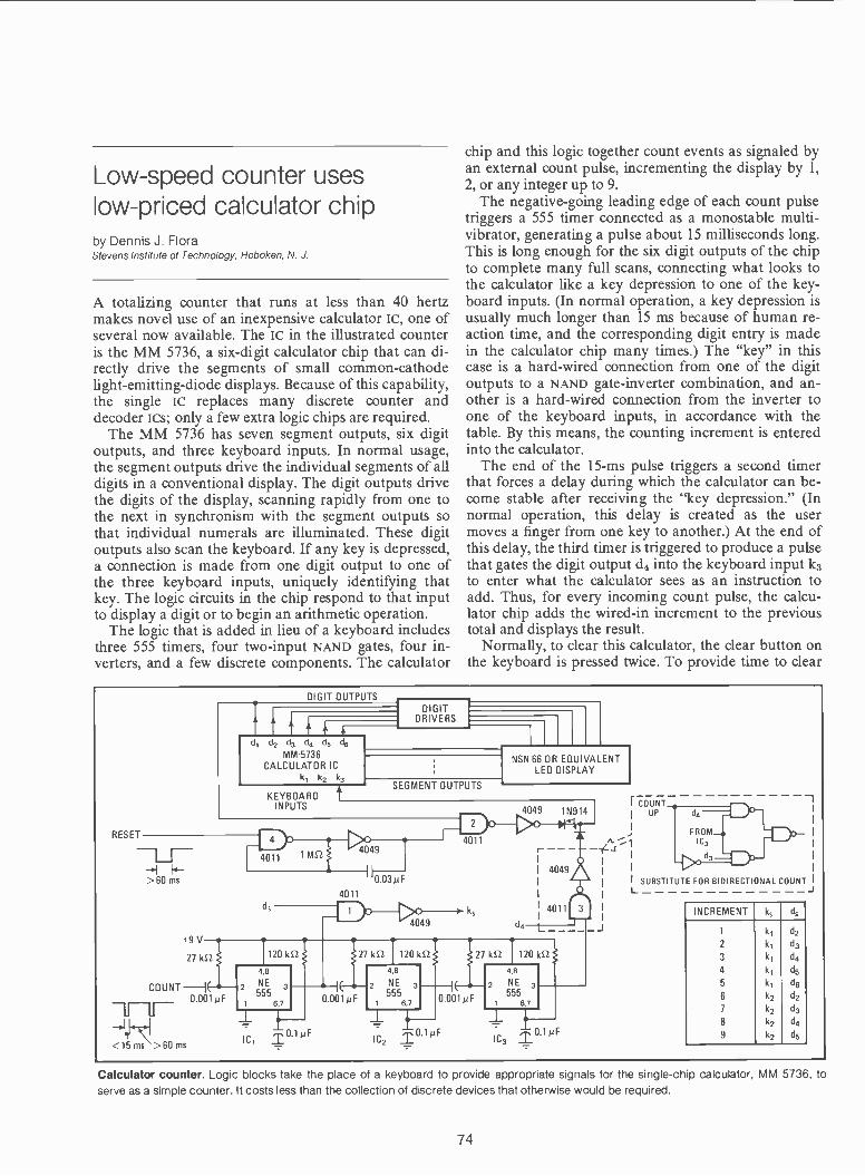
Low -speed counter useslow-priced calculator chipby Dennis J. FloraStevens Institute of Technology, Hoboken, N. J.
A totalizing counter that runs at less than 40 hertzmakes novel use of an inexpensive calculator lc, one ofseveral now available. The Ic in the illustrated counteris the MM 5736, a six -digit calculator chip that can di-rectly drive the segments of small common -cathodelight -emitting -diode displays. Because of this capability,the single Ic replaces many discrete counter anddecoder ics; only a few extra logic chips are required.
The MM 5736 has seven segment outputs, six digitoutputs, and three keyboard inputs. In normal usage,the segment outputs drive the individual segments of alldigits in a conventional display. The digit outputs drivethe digits of the display, scanning rapidly from one tothe next in synchronism with the segment outputs sothat individual numerals are illuminated. These digitoutputs also scan the keyboard. If any key is depressed,a connection is made from one digit output to one ofthe three keyboard inputs, thatkey. The logic circuits in the chip respond to that inputto display a digit or to begin an arithmetic operation.
The logic that is added in lieu of a keyboard includesthree 555 timers, four two -input NAND gates, four in-verters, and a few discrete components. The calculator
chip and this logic together count events as signaled byan external count pulse, incrementing the display by 1,2, or any integer up to 9.
The negative -going leading edge of each count pulsetriggers a 555 timer connected as a monostable multi -vibrator, generating a pulse about 15 milliseconds long.This is long enough for the six digit outputs of the chipto complete many full scans, connecting what looks tothe calculator like a key depression to one of the key-board inputs. (In normal operation, a key depression isusually much longer than 15 ms because of human re-action time, and the corresponding digit entry is madein the calculator chip many times.) The "key" in thiscase is a hard -wired connection from one of the digitoutputs to a NAND gate -inverter combination, and an-other is a hard -wired connection from the inverter toone of the keyboard inputs, in accordance with thetable. By this means, the counting increment is enteredinto the calculator.
The end of the 15 -ms pulse triggers a second timerthat forces a delay during which the calculator can be-come stable after receiving the "key depression." (Innormal operation, this delay is created as the usermoves a finger from one key to another.) At the end ofthis delay, the third timer is triggered to produce a pulsethat gates the digit output d4 into the keyboard input k3to enter what the calculator sees as an instruction toadd. Thus, for every incoming count pulse, the calcu-lator chip adds the wired -in increment to the previoustotal and displays the result.
Normally, to clear this calculator, the clear button onthe keyboard is pressed twice. To provide time to clear
RESET
DIGIT OUTPUTS
d2 d3 d4 d5 d6
MM -5736CALCULATOR IC
k1 k2 k3
DIGITDRIVERS
KEYBOARDINPUTS
SEGMENT OUTPUTS
NSN 66 OR EQUIVALENTLED DISPLAY
-01 14-> 60 ms
+9 V
4011 1 MS24049
0.0311F
4011
U.4011
4049
ks
4049 1N914
rs,
4
4049
4011
27 k1-2
COUNT0.001µF
<15 ms >60 ms IC, ±0.1µF
48
2 N E 3
5550.001 ME
27 kS2 120 kEl
48
2 NE 3
5551 6,7
IC20.1µF
27 kS2 120 kS2
0.001 µF
4,8
2 NE 3
5556,7
0 1 FIC3 2
COUNTI UP
-11--r
J
1
I SUBSTITUTE FOR BIDIRECTIONAL COUNTL J
INCREMENT ks ds
1 k, d2
2 k, d3
3 k, d4
4 k, d5
5 k, d6
6 k2 d2
7 k2 d3
8 k2 d4
9 k2 d5
Calculator counter. Logic blocks take the place of a keyboard to provide appropriate signals for the single -chip calculator, MM 5736, toserve as a simple counter. It costs less than the collection of discrete devices that otherwise would be required.
74
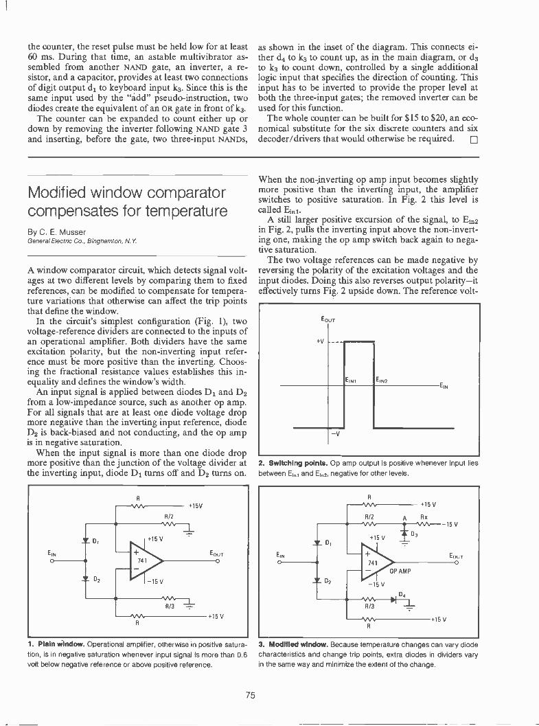
the counter, the reset pulse must be held low for at least60 ms. During that time, an astable multivibrator as-sembled from another NAND gate, an inverter, a re-sistor, and a capacitor, provides at least two connectionsof digit output d1 to keyboard input k3. Since this is thesame input used by the "add" pseudo -instruction, twodiodes create the equivalent of an OR gate in front of k3.
The counter can be expanded to count either up ordown by removing the inverter following NAND gate 3and inserting, before the gate, two three -input NANDs,
as shown in the inset of the diagram. This connects ei-ther d4 to k3 to count up, as in the main diagram, or d3to k3 to count down, controlled by a single additionallogic input that specifies the direction of counting. Thisinput has to be inverted to provide the proper level atboth the three -input gates; the removed inverter can beused for this function.
The whole counter can be built for $15 to $20, an eco-nomical substitute for the six discrete counters and sixdecoder/drivers that would otherwise be required.
Modified window comparatorcompensates for temperatureBy C. E. MusserGeneral Electric Co., Binghamton, N.Y.
A window comparator circuit, which detects signal volt-ages at two different levels by comparing them to fixedreferences, can be modified to compensate for tempera-ture variations that otherwise can affect the trip pointsthat define the window.
In the circuit's simplest configuration (Fig. 1), twovoltage -reference dividers are connected to the inputs ofan operational amplifier. Both dividers have the sameexcitation polarity, but the non -inverting input refer-ence must be more positive than the inverting. Choos-ing the fractional resistance values establishes this in-equality and defines the window's width.
An input signal is applied between diodes D1 and D2from a low -impedance source, such as another op amp.For all signals that are at least one diode voltage dropmore negative than the inverting input reference, diodeD2 is back -biased and not conducting, and the op ampis in negative saturation.
When the input signal is more than one diode dropmore positive than the junction of the voltage divider atthe inverting input, diode D1 turns off and D2 turns on.
1. Plain window. Operational amplifier, otherwise in positive satura-tion, is in negative saturation whenever input signal is more than 0.6volt below negative reference or above positive reference.
When the non -inverting op amp input becomes slightlymore positive than the inverting input, the amplifierswitches to positive saturation. In Fig. 2 this level iscalled Em1.
A still larger positive excursion of the signal, to Ein2in Fig. 2, pulls the inverting input above the non -invert-ing one, making the op amp switch back again to nega-tive saturation.
The two voltage references can be made negative byreversing the polarity of the excitation voltages and theinput diodes. Doing this also reverses output polarity-iteffectively turns Fig. 2 upside down. The reference volt -
2. Switching points. Op amp output is positive whenever input liesbetween E,,1 and Em2, negative for other levels.
3. Modified window. Because temperature changes can vary diodecharacteristics and change trip points, extra diodes in dividers varyin the same way and minimize the extent of the change.
75

ages for this circuit are
Ein1 = 11(R/3)/(R +R/3)] - Vd = (V/4)- Vd
Em2 = V[(R/2)/(R+R/2)1+ Vd = (V/3)+ Vd
where Vd is the diode voltage drop.Temperature changes cause diode variation that af-
fect the trip points. Additional diodes in the dividers(Fig. 3) vary in the same way as the input diodes, andthus partially compensate for such changes. The resistorRx should be chosen so that point A is slightly negative,just enough to bias the diode into continuous conduc-
tion. For the modified circuit the reference voltages are
= - Vd)(R/3)/(R + R/3)] + Vd0 - Vd
= (V - Vd)/4Em2 = 11[(V Vd)(R/2)/(R + R/2)] - VdO + Vd
= (V +Vd)/3
Both of these circuit versions have been tested atroom temperature using -±1% metal -film resistors,1N4148 diodes, and 741 op amps. Assuming Vd to be0.6 volts, the measured trip points agreed well with thecalculated values. El
Timer pulse widths rangefrom seconds to hoursby Ken EricksonInterstate Electronics Corp., Anaheim, Calif.
A timer with output durations ranging from a few sec-onds to more than 100 hours can be built around a pla-ting cell, thus avoiding the special low -leakage compo-nents or high resistances that such timers often require.
When the current direction in a plating cell is fromreservoir electrode to working electrode, silver is platedonto the working electrode in an amount proportionalto the charge passed through the cell. Conversely, whenthe current direction is from working electrode to reser-voir electrode, silver is removed from the working elec-trode. As long as the electrode is plated, the impedanceof the cell is only a few kilohms; but after all the platingis removed from the anode, the impedance across thecell increases to several megohms. When this happens,transistor Qi is turned on; otherwise, when the cell isplated, Qi is cut off.
The plating charge is the charge on capacitor C.When the input and output have both been low for along time, C has charged fully to about 3.6 volts, and at1,000 microfarads as shown, it holds 3.6 x 10⁻³ cou-lomb. Then, when the external input to gate Gi goeshigh, its output drops to ground, and C discharges
through the plating cell. The current, Id, with the refer-ence shown, is negative, causing the cell to be plated.The current's magnitude is limited by resistor RI; thetime constant for the values shown is about 1 second.Plating the cell drops the voltage at the base of Qi be-low its threshold, thus turning Qi off and Q2 on. Thecollector of Q2 drops almost to ground; this level is in-verted by gate G2, and the output goes high. This out-put feeds back to gate G1 to make the circuit's operationindependent of the input line once the timing cycle hasbegun.
The deplating current flows continuously through R2;it is 1 microampere for the value of R2 shown. Whendeplating is nearly completed, the cell's impedance be-gins increasing gradually, Qi turns back on, the timeroutput goes low, and if the timer input is low, capacitorC charges again.
The charge transferred during either plating or de -plating is represented by
Q = CV = IdTFrom this relationship, the time to transfer this charge is
T = CV/Id
For a 1,000-microfarad capacitor, the time to deplatethe cell is 3,600 seconds-a full hour. Other times can beobtained by using different values for the capacitor C orthe resistor R2. El
INPUT C
+ 1
1 l(S2%7402 6V
WORKING ELECTRODE
RESERVOIR ELECTRODE
+5 Vdc
R2 A3
5.1 K2 150a2
RI u
Id
2N2484
INPUT4 V
0 V
OUTPUT 4 V0V
T
NOTE: PI IS PLESSEY ELECTRO-PRODUCTS E -CELL 560-0002
Wide range. Timer output can be as short as a few seconds or aslong as many hours, by choice of RC time constant. Pulse width isnot affected even if leaky capacitor is used, because circuit's oper-ation is based on deposition and removal of silver in plating cell P1.
76
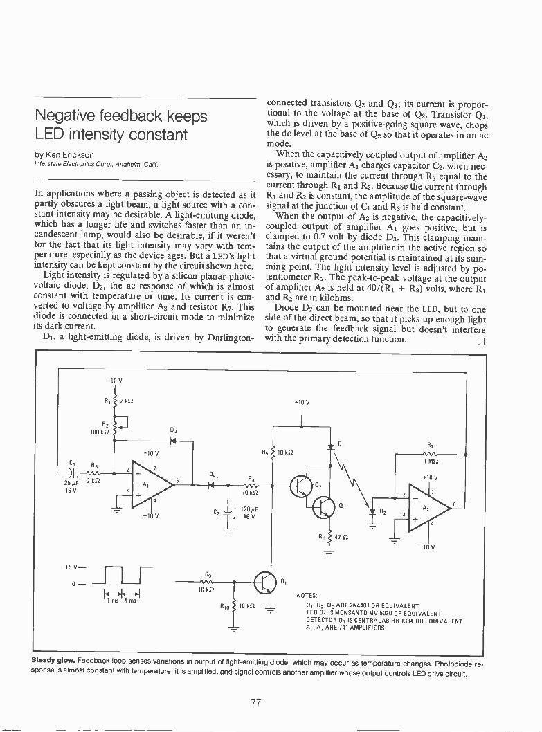
Negative feedback keepsLED intensity constantby Ken EricksonInterstate Electronics Corp., Anaheim, Calif.
In applications where a passing object is detected as itpartly obscures a light beam, a light source with a con-stant intensity may be desirable. A light -emitting diode,which has a longer life and switches faster than an in-candescent lamp, would also be desirable, if it weren'tfor the fact that its light intensity may vary with tem-perature, especially as the device ages. But a LED's lightintensity can be kept constant by the circuit shown here.
Light intensity is regulated by a silicon planar photo-voltaic diode, D2, the ac response of which is almostconstant with temperature or time. Its current is con-verted to voltage by amplifier A2 and resistor R7. Thisdiode is connected in a short-circuit mode to minimizeits dark current.
Di, a light -emitting diode, is driven by Darlington -
connected transistors Q2 and Q3; its current is propor-tional to the voltage at the base of Q2. Transistor Qi,which is driven by a positive -going square wave, chopsthe dc level at the base of Q2 so that it operates in an acmode.
When the capacitively coupled output of amplifier A2is positive, amplifier Ai charges capacitor C2, when nec-essary, to maintain the current through R3 equal to thecurrent through R1 and R2. Because the current throughR1 and R2 is constant, the amplitude of the square -wavesignal at the junction of C1 and R3 is held constant.
When the output of A2 is negative, the capacitively-coupled output of amplifier Al goes positive, but isclamped to 0.7 volt by diode D3. This clamping main-tains the output of the amplifier in the active region sothat a virtual ground potential is maintained at its sum-ming point. The light intensity level is adjusted by po-tentiometer R2. The peak -to -peak voltage at the outputof amplifier A2 is held at 40/(R1 + R2) volts, where R1and R2 are in kilohms.
Diode D2 can be mounted near the LED, but to oneside of the direct beam, so that it picks up enough lightto generate the feedback signal but doesn't interferewith the primary detection function. 0
+5 V-
0 -II 011 '1lms i MS
-10 V
-10 V
NOTES:
10 l(S-2. 01, 02, 03 ARE 2N4401 OR EQUIVALENTLED DI IS MONSANTO MV 5020 OR EQUIVALENTDETECTOR 02 IS CENTRALAB HR 1334 OR EQUIVALENTA1, A2 ARE 741 AMPLIFIERS
Steady glow. Feedback loop senses variations in output of light -emitting diode, which may occur as temperature changes. Photodiode re-sponse is almost constant with temperature; it is amplified, and signal controls another amplifier whose output controls LED drive circuit.
77
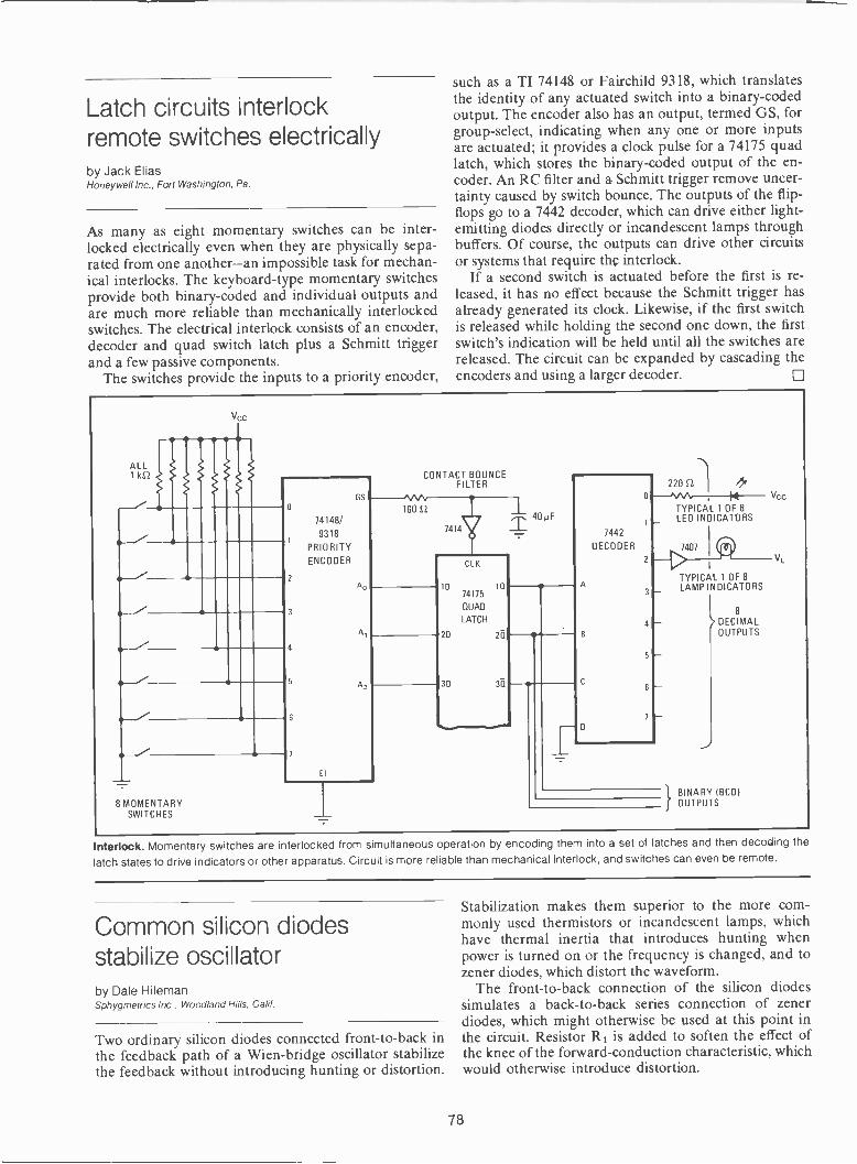
Latch circuits interlockremote switches electricallyby Jack EliasHoneywell Inc., Fort Washington, Pa
As many as eight momentary switches can be inter-locked electrically even when they are physically sepa-rated from one another-an impossible task for mechan-ical interlocks. The keyboard -type momentary switchesprovide both binary-coded and individual outputs andare much more reliable than mechanically interlockedswitches. The electrical interlock consists of an encoder,decoder and quad switch latch plus a Schmitt triggerand a few passive components.
The switches provide the inputs to a priority encoder,
such as a TI 74148 or Fairchild 9318, which translatesthe identity of any actuated switch into a binary-codedoutput. The encoder also has an output, termed GS, forgroup -select, indicating when any one or more inputsare actuated; it provides a clock pulse for a 74175 quadlatch, which stores the binary-coded output of the en-coder. An RC filter and a Schmitt trigger remove uncer-tainty caused by switch bounce. The outputs of the flip-flops go to a 7442 decoder, which can drive either light -emitting diodes directly or incandescent lamps throughbuffers. Of course, the outputs can drive other circuitsor systems that require the interlock.
If a second switch is actuated before the first is re-leased, it has no effect because the Schmitt trigger hasalready generated its clock. Likewise, if the first switchis released while holding the second one down, the firstswitch's indication will be held until all the switches arereleased. The circuit can be expanded by cascading theencoders and using a larger decoder. 0
ALL1 kS2
8 MOMENTARYSWITCHES
vcc
0
2
3
4
5
6
7
74148/
9318
PRIORITY
ENCODER
El
GS
Ao
A,
A,
CONTACT BOUNCEFILTER
16087
7414
10
20
3D
CLK
74175
QUAD
LATCH
113
7(1
40µF
-
A
7442
DECODER
0
3
4
5
6
7
220 SZ
Vcc
TYPICAL 1 OF 8LED INDICATORS
TYPICAL 1 OF 8LAMP INDICATORS
8
>DECIMALOUTPUTS
_J
BINARY (BCD)OUTPUTS
Interlock. Momentary switches are interlocked from simultaneous operation by encoding them into a set of latches and then decoding the
latch states to drive indicators or other apparatus. Circuit is more reliable than mechanical interlock, and switches can even be remote.
Common silicon diodesstabilize oscillatorby Dale HilemanSphygrnetrics Inc., Woodland Hills, Calif.
Two ordinary silicon diodes connected front -to -back inthe feedback path of a Wien -bridge oscillator stabilizethe feedback without introducing hunting or distortion.
Stabilization makes them superior to the more com-monly used thermistors or incandescent lamps, whichhave thermal inertia that introduces hunting whenpower is turned on or the frequency is changed, and tozener diodes, which distort the waveform.
The front -to -back connection of the silicon diodessimulates a back-to-back series connection of zenerdiodes, which might otherwise be used at this point inthe circuit. Resistor R1 is added to soften the effect ofthe knee of the forward -conduction characteristic, whichwould otherwise introduce distortion.
78
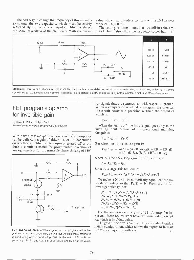
The best way to change the frequency of this circuit isto change the two capacitors, which must be closelymatched. By this means, the output amplitude is alwaysthe same, regardless of the frequency. With the circuit
values shown, amplitude is constant within ±0.3 dB overrange of 100,000 to 1.
The setting of potentiometer R2 establishes the am-plitude, but it also affects the frequency somewhat. p
R2
10 IQ 10 kl2 100 kfl
C f
_100 pF 5 kHz
7411000 pF 500 Hz+-
C
.
1 MS2..----.
0.01 µF 50 Hz
0 1N'i141 MS2 04 ii 0.1µF
1µF
10µF
5 Hz
0.5 Hz
0.05 Hz
C 100 kSt1=0,
14
1N914
Stabilizer. Front -to -back diodes in oscillator's feedback path acts as stabilizer, yet do not cause hunting or distortion, as lamps or zenerssometimes do. Capacitors, which control frequency, are matched; amplitude control is by potentiometer, which also affects frequency.
FET programs op ampfor invertible gainby Ken A. Dill and Mark TrollRevelle College, University of California, La Jolla, Calif,
With only a few inexpensive components, an amplifiercan be built with a gain of either +N or -N, dependingon whether a field-effect transistor is turned off or on.Such a circuit is useful for programable inversion ofanalog signals or for programable phase -shifting of 180°
FET inverts op amp. Amplifier gain can be programmed eitherpositive or negative, depending on whether the field-effect transistoris conducting or not conducting. Gain is the ratio of Rf to R; forgains of ±1, Rf, R2, and R3 are all equal value, and R1 is half the value.
for signals that are symmetrical with respect to ground.When a comparator is added to program the inverter,the circuit becomes a precision rectifier, the output ofwhich is:
Vout = I vin Vred
When the FET is off, the input signal goes only to theinverting input terminal of the operational amplifier;the gain is:
Kw/ Vin = - Rf/ R
But when the FET is on, the gain is:
Vout/ Vin = nA/[1 + (ARRI)/(RiRf + RRf +RRi)l0x [f - )111110/(R1R1 +REtt- +RRI)]
where A is the open -loop gain of the op amp, and
f = R3/ (R2 + R3)
Since A is large, this reduces to:
Vont/ Vin = I Of/ R) 1[(Rf /R0+ 1]
To make +N and -N numerically equal, choose theresistance values so that ROI = N. From that, it fol-lows algebraically that:
N = (f- 1)(N) + 11(NR/ Ri)+ 1]2N = fN + (fNR/ Ri) + f2N Ri = fNRi + fNR + fRi2N Ri -fNRi -JR' = fNRR1 = NRf/[2N -(N + 1 )1]
For the simplest case-a gain of ±-1-all amplifier in-put and feedback resistors have the same value, exceptR1, which is half that value.
The gate of the FET is controlled by a standard analogswitch configuration, which allows the inputs to be 0 or+5 volts, compatible with TTL. 0
79

Digital -to -analog convertercontrols active filterby Jerry WhitmoreAnalog Devices, Santa Clara, Calif.
A monolithic digital -to -analog converter can be thecontrol element of an active filter. Shown in Fig. 1 is acircuit that generates a low-pass, single pole that can bemoved over a dynamic frequency range of 2n:1, where nis the resolution in bits of the d -a converter. If, for ex-ample, a converter with 10 -bit resolution is used in thiscircuit, dynamic range is 1,024:1.
An equivalent simplified version of Fig. 1 is shown inFig. 2(a), where R4 and R3 take on the values shown.Riadder isthe characteristic resistance of the R -2R lad-der of the d -a converter and the coefficients A assume avalue of 1 for an on bit, and zero for an off bit. Notethat R4 in parallel with R3 equals Bladder.
The circuit, consisting of R4, C, and the amplifier, canbe treated as a gain block as shown in Fig. 2(b). At fre-quencies above the open -loop corner, the response ofthe gain block is A(co) = Vout/V2 or about 1/6)114C. Itsunity gain bandwidth is FGBW = 0.159/R4C.
Frequency response of a closed -loop amplifier is F3dB= BfGBW where B is the amplifier feedback attenuationratio. Using the unity gain bandwidth of the gain blockand the system B results in the filter closed loop fre-quency response equations shown in Fig. 2(b).
1. 1,024:1. An active low-pass filter such as this, built around an op-erational amplifier, passive components, and a 10 -bit digital -to -analog converter, has a dynamic -frequency range of 1,024:1.
R,
VIN
(al
RA
RLADDER
(A1/2' + A2/22 + An/2")
R LADDERR3 -
(Ai /2' + A2/22 + An/2")
03
VOUT
+ + + .14
0.159SYSTEM f -3 dB
NC (1 + R2/RI + R2/R3 + R2/R4)
R,
VIN
( b )
R
V2
0.159
R4C (1 + ROI LADDER + R2/R1)
EQUIVALENT GAIN BLOCK1/wR4C
UNITY -GAIN BW = fGBw = 0.159/R4COF GAIN BLOCK
VOUT
2. Equivalent circuits. The d -a of (1) can be replaced by the circuitwithin the dashed lines (a). A further simplification (b) lumps R4, Cand the op amp into a gain block.
80
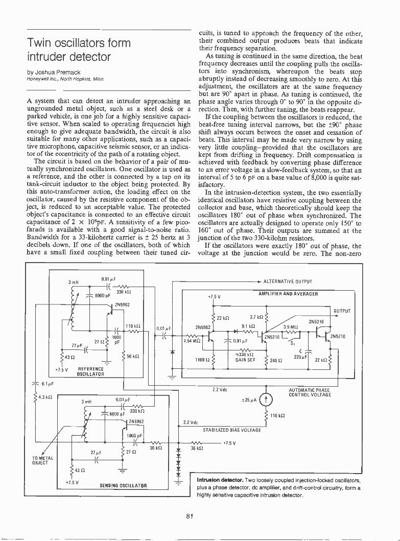
Twin oscillators formintruder detectorby Joshua PremackHoneywell Inc., North Hopkins, Minn.
A system that can detect an intruder approaching anungrounded metal object, such as a steel desk or aparked vehicle, is one job for a highly sensitive capaci-tive sensor. When scaled to operating frequencies highenough to give adequate bandwidth, the circuit is alsosuitable for many other applications, such as a capaci-tive microphone, capacitive seismic sensor, or an indica-tor of the eccentricity of the path of a rotating object.
The circuit is based on the behavior of a pair of mu-tually synchronized oscillators. One oscillator is used asa reference, and the other is connected by a tap on itstank -circuit inductor to the object being protected. Bythis auto -transformer action, the loading effect on theoscillator, caused by the resistive component of the ob-ject, is reduced to an acceptable value. The protectedobject's capacitance is connected to an effective circuitcapacitance of 2 X 10⁶pF. A sensitivity of a few pico-farads is available with a good signal-to-noise ratio.Bandwidth for a 33 -kilohertz carrier is ± 25 hertz at 3decibels down. If one of the oscillators, both of whichhave a small fixed coupling between their tuned cir-
cuits, is tuned to approach the frequency of the other,their combined output produces beats that indicatetheir frequency separation.
As tuning is continued in the same direction, the beatfrequency decreases until the coupling pulls the oscilla-tors into synchronism, whereupon the beats stopabruptly instead of decreasing smoothly to zero. At thisadjustment, the oscillators are at the same frequencybut are 90° apart in phase. As tuning is continued, thephase angle varies through 0° to 90° in the opposite di-rection. Then, with further tuning, the beats reappear.
If the coupling between the oscillators is reduced, thebeat -free tuning interval narrows, but the ±90° phaseshift always occurs between the onset and cessation ofbeats. This interval may be made very narrow by usingvery little coupling-provided that the oscillators arekept from drifting in frequency. Drift compensation isachieved with feedback by converting phase differenceto an error voltage in a slow -feedback system, so that aninterval of 5 to 6 pF on a base value of 8,000 is quite sat-isfactory.
In the intrusion -detection system, the two essentiallyidentical oscillators have resistive coupling between thecollector and base, which theoretically should keep theoscillators 180° out of phase when synchronized. Theoscillators are actually designed to operate only 150° to160° out of phase. Their outputs are summed at the
junction of the two 330-kilohm resistors.If the oscillators were exactly 180° out of phase, the
voltage at the junction would be zero. The non -zero
3 mH0.01µF
II330 k12
,--, 8000 pF
2N5962
110 kE2
27µF
4352
+7.5 V
27 S2
REFERENCEOSCILLATOR
1000pF
56 kS2
4.3 kE2
0.01µF-
ALTERNATIVE OUTPUT
+7.5 V
2N5962
1.54 M'2
1100E2
AMPLIFIER AND AVERAGER
22 kt2
OUTPUT
2.7 kE2
9.1 kE2 3.9 MS1
2N5210
=330 k12GAIN SET 240 E2
2N5210
C
220 µF22 kt2
2N5210
3 mH 0.0 /IF
31(118000 pF
30
TO METALOBJECT
27µF 27E2
43 E2
+7.5 VSENSING OSCILLATOR
2N5962
1000 pF
-'sAA..--/VVV- +7.5 V36 kE2 36 kE2
I
2.2 Vdc
2.2 Vdc
±25
STABILIZED BIAS VOLTAGE
AUTOMATIC PHASECONTROL VOLTAGE
110 kE2
Intrusion detector. Two loosely coupled injection -locked oscillators,plus a phase detector, dc amplifier, and drift -control circuitry, form ahighly sensitive capacitive intrusion detector.
81
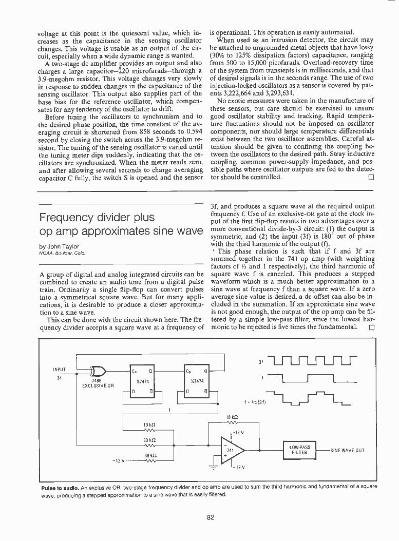
voltage at this point is the quiescent value, which in-creases as the capacitance in the sensing oscillatorchanges. This voltage is usable as an output of the cir-cuit, especially when a wide dynamic range is wanted.
A two -stage dc amplifier provides an output and alsocharges a large capacitor -220 microfarads-through a3.9-megohm resistor. This voltage changes very slowlyin response to sudden changes in the capacitance of thesensing oscillator. This output also supplies part of thebase bias for the reference oscillator, which compen-sates for any tendency of the oscillator to drift.
Before tuning the oscillators to synchronism and tothe desired phase position, the time constant of the av-eraging circuit is shortened from 858 seconds to 0.594second by closing the switch across the 3.9-megohm re-sistor. The tuning of the sensing oscillator is varied untilthe tuning meter dips suddenly, indicating that the os-cillators are synchronized. When the meter reads zero,and after allowing several seconds to charge averagingcapacitor C fully, the switch S is opened and the sensor
is operational. This operation is easily automated.When used as an intrusion detector, the circuit may
be attached to ungrounded metal objects that have lossy(30% to 125% dissipation factors) capacitance, rangingfrom 500 to 15,000 picofarads. Overload -recovery timeof the system from transients is in milliseconds, and thatof desired signals is in the seconds range. The use of twoinjection -locked oscillators as a sensor is covered by pat-ents 3,222,664 and 3,293,631.
No exotic measures were taken in the manufacture ofthese sensors, but care should be exercised to ensuregood oscillator stability and tracking. Rapid tempera-ture fluctuations should not be imposed on oscillatorcomponents, nor should large temperature differentialsexist between the two oscillator assemblies. Careful at-tention should be given to confining the coupling be-tween the oscillators to the desired path. Stray inductivecoupling, common power -supply impedance, and pos-sible paths where oscillator outputs are fed to the detec-tor should be controlled.
Frequency divider plusop amp approximates sine waveby John TaylorNOAA, Boulder, Colo.
A group of digital and analog integrated circuits can becombined to create an audio tone from a digital pulsetrain. Ordinarily a single flip-flop can convert pulsesinto a symmetrical square wave. But for many appli-cations, it is desirable to produce a closer approxima-tion to a sine wave.
This can be done with the circuit shown here. The fre-quency divider accepts a square wave at a frequency of
3f, and produces a square wave at the required outputfrequency f. Use of an exclusive-oR gate at the clock in-put of the first flip-flop results in two advantages over amore conventional divide -by -3 circuit: (1) the output issymmetric, and (2) the input (30 is 180° out of phasewith the third harmonic of the output (f). This phase relation is such that if f and 3f are
summed together in the 741 op amp (with weightingfactors of 1/3 and 1 respectively), the third harmonic ofsquare wave f is canceled. This produces a steppedwaveform which is a much better approximation to asine wave at frequency f than a square wave. If a zeroaverage sine value is desired, a dc offset can also be in-cluded in the summation. If an approximate sine waveis not good enough, the output of the op amp can be fil-tered by a simple low-pass filter, since the lowest har-monic to be rejected is five times the fundamental.
INPUT
3f7486
EXCLUSIVE ORY:7474
Cp
'0474
3f
f
f +1/3130
I
10 kS2
10 kS2
+12 V
30 kElAAA. LOW-PASS
FILTER36 kS2
741 SINE WAVE OUT
-12 V-12 V
Pulse to audio. An exclusive OR, two -stage frequency divider and op amp are used to sum the third harmonic and fundamental of a square
wave, producing a stepped approximation to a sine wave that is easily filtered.
82
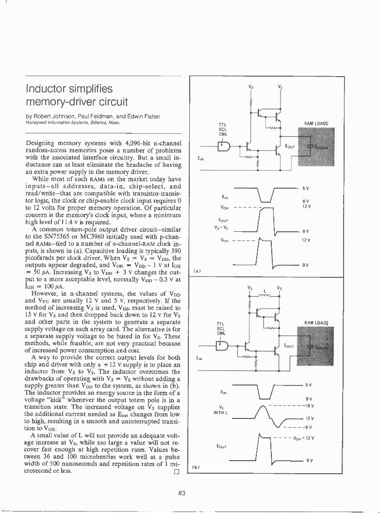
Inductor simplifiesmemory -driver circuitby Robert Johnson, Paul Feldman, and Edwin FisherHoneywell Information Systems, Billerica, Mass.
Designing memory systems with 4,096 -bit n -channelrandom-access memories poses a number of problemswith the associated interface circuitry. But a small in-ductance can at least eliminate the headache of havingan extra power supply in the memory driver.
While most of such RAMS on the market today haveinputs-all addresses, data -in, chip -select, andread/write-that are compatible with transistor -transis-tor logic, the clock or chip -enable clock input requires 0to 12 volts for proper memory operation. Of particularconcern is the memory's clock input, where a minimumhigh level of 11.4 v is required.
A common totem -pole output driver circuit-similarto the SN75365 or MC3960 initially used with p -chan-nel RAMS-tied to a number of n -channel -RAM clock in-puts, is shown in (a). Capacitive loading is typically 390picofarads per clock driver. When V2 = V3 = VDD, theoutputs appear degraded, and VW; = VDD - 1 v at Lax= 50 µA. Increasing V3 to VDD + 3 v changes the out-put to a more acceptable level, normally VDD - 0.3 v atIOU = 100 ILA.
However, in n -channel systems, the values of VDDand Vec are usually 12 v and 5 v, respectively. If themethod of increasing V3 is used, VDD must be raised to15 v for V3 and then dropped back down to 12 v for V2and other parts in the system to generate a separatesupply voltage on each array card. The alternative is fora separate supply voltage to be bused in for V3. Thesemethods, while feasible, are not very practical becauseof increased power consumption and cost.
A way to provide the correct output levels for bothchip and driver with only a + 12 v supply is to place aninductor from V3 to V2. The inductor overcomes thedrawbacks of operating with V3 = V2 without adding asupply greater than VDD to the system, as shown in (b).The inductor provides an energy source in the form of avoltage "kick" whenever the output totem pole is in atransition state. The increased voltage on V3 suppliesthe additional current needed as Eout changes from lowto high, resulting in a smooth and uninterrupted transi-tion to VOH
A small value of L will not provide an adequate volt-age increase at V3, while too large a value will not re-cover fast enough at high repetition rates. Values be-tween 36 and 100 microhenries work well at a pulsewidth of 500 nanoseconds and repetition rates of 1 mi-crosecond or less.
EIN
VOH
EOUT
V3 = V2
VOH
(a)
V3 V2
5V
0 V12 V
0 V
12 V
0 V
TTLECLCML
EIN
Eiry
V3
WITH L
EoUT
( b )
V3 V2
RAM LOADS
5V
0 V
18 V
12V
- - - - \km =12V
0 V
83
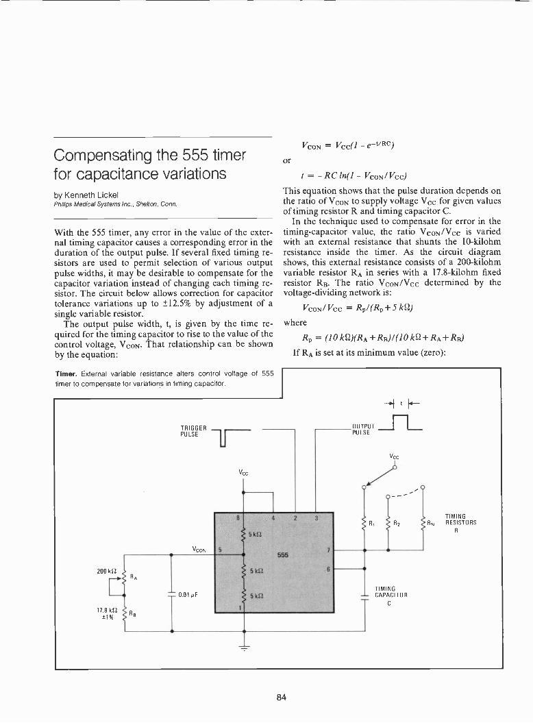
Compensating the 555 timerfor capacitance variationsby Kenneth LickelPhilips Medical Systems Inc., Shelton, Conn.
With the 555 timer, any error in the value of the exter-nal timing capacitor causes a corresponding error in theduration of the output pulse. If several fixed timing re-sistors are used to permit selection of various outputpulse widths, it may be desirable to compensate for thecapacitor variation instead of changing each timing re-sistor. The circuit below allows correction for capacitortolerance variations up to ± 12.5% by adjustment of asingle variable resistor.
The output pulse width, t, is given by the time re-quired for the timing capacitor to rise to the value of thecontrol voltage, Yam. That relationship can be shownby the equation:
Timer. External variable resistance alters control voltage of 555timer to compensate for variations in timing capacitor.
V00/4 = VcC(/ -
or
= - RC Ina - VcoN/ Ilec)
This equation shows that the pulse duration depends onthe ratio of VcoN to supply voltage Vcc for given valuesof timing resistor R and timing capacitor C.
In the technique used to compensate for error in thetiming -capacitor value, the ratio VcoN/Vcc is variedwith an external resistance that shunts the 10-kilohmresistance inside the timer. As the circuit diagramshows, this external resistance consists of a 200-kilohmvariable resistor RA in series with a 17.8-kilohm fixedresistor RB. The ratio VcoN/Vcc determined by thevoltage -dividing network is:
VcoN/ Vcc = Rp/(Rp+ 5 kS2)
where
Rp = kSVRA +RB)/(10 lc2+ RA RB)
If RA is set at its minimum value (zero):
200 {cf.?.
TRIGGERPULSE -11-
VcoN
17.8 kS2±1%
0.01 1.1F
5 k52
555
51(52,
5 k12
OUTPUTPULSE
--I
TIMINGCAPACITOR
TIMINGRESISTORS
R
84

Rp = 6.4 IcSI
and
VcON/ Vcc = 0.56
Therefore, the pulse duration is
train = 0.83 RC
Similarly, if RA is set at its maximumkilohms), the pulse duration is:
tmax = 1.07 RC
value (200
Thus the variation of RA can vary the output -pulsewidth by ± 12.5% about a nominal value of (0.83 +1.07)RC/2. For the circuit shown, therefore, the nomi-nal width of the output pulse is:
tnom = 0.95 RC
If values for the timing resistors and capacitor are cal-culated from this formula, then capacitor variations of± 12.5% can be compensated by adjustment of RA. Ifwider tolerances are desired, RB must be reduced; newvalues must then be calculated for Rp, VcoN/VCC, tmin,tmax, and tnom
Generating overlapped clockphases for CCD arrayby Hans-Jorg Pfleiderer and K. KnauerSiemens AG, Munich, Germany
Arrays of three-phase charge -coupled devices requireoverlapped clock pulses (Fig. 1) for satisfactory oper-ation. To generate these overlapped pulses, FairchildSemiconductor, which produces the arrays commer-cially, suggests a rather complicated logic circuit in a re-port that it circulates.
But a less complicated circuit (Fig. 2) can also gener-ate the train of overlapped pulses, as shown in the tim-ing chart (Fig. 3). When the master clock pulse goeshigh, J -K flip-flop FF1 turns on only if the outputs Qiand Q2 are both low. With FF1 on, Qi rises, opening thegate so that the rise of the next master clock pulse turnson FF2, without affecting FF1. However, with Q2 up,
1. Overlap. Arrays of three-phase charge -coupled devices requireoverlapping pulse trains for proper operation. The logic to producethese trains does not have to be complicated-it need not involvemore than three flip-flops and a few gates.
2. Pulse -train generator. When the master clock's pulse rises, one flip-flop turns on, gated by the state of the flip-flop before it. When thepulse falls, the preceding flip-flop turns off, this time gated by the state of the following flip-flop.
85
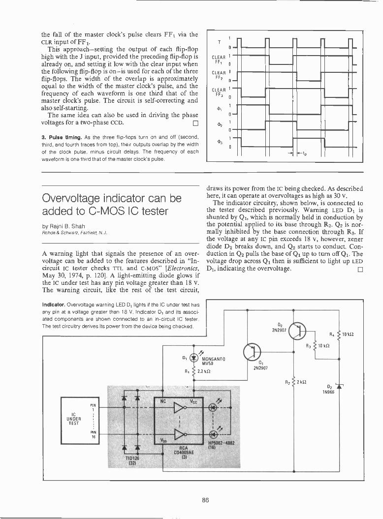
the fall of the master clock's pulse clears FF1 via theCLR input of FF1.
This approach-setting the output of each flip-flophigh with the J input, provided the preceding flip-flop isalready on, and setting it low with the clear input whenthe following flip-flop is on-is used for each of the threeflip-flops. The width of the overlap is approximatelyequal to the width of the master clock's pulse, and thefrequency of each waveform is one third that of themaster clock's pulse. The circuit is self-correcting andalso self-starting.
The same idea can also be used in driving the phasevoltages for a two-phase CCD.
3. Pulse timing. As the three flip-flops turn on and off (second,third, and fourth traces from top), their outputs overlap by the widthof the clock pulse, minus circuit delays. The frequency of eachwaveform is one third that of the master clock's pulse.
T
CLEARFF1
CLEARFF2
CLEARFF3
(1,3
r0
1
1
0
0
1
0
o I
-4" 4-tn
Overvoltage indicator can beadded to C-MOS IC testerby Rajni B. ShahRohde & Schwarz, Fairfield, N.J.
A warning light that signals the presence of an over -voltage can be added to the features described in "In -circuit IC tester checks TTL and C-MOS" [Electronics,May 30, 1974, p. 120]. A light -emitting diode glows ifthe lc under test has any pin voltage greater than 18 v.The warning circuit, like the rest of the test circuit,
Indicator. Overvoltage warning LED D1 lights if the IC under test hasany pin at a voltage greater than 18 V. Indicator D1 and its associ-ated components are shown connected to an in -circuit IC tester.The test circuitry derives its power from the device being checked.
draws its power from the IC being checked. As describedhere, it can operate at overvoltages as high as 30 v.
The indicator circuitry, shown below, is connected tothe tester described previously. Warning LED D1 isshunted by Qi, which is normally held in conduction bythe potential applied to its base through R2. Q2 is nor-mally inhibited by the base connection through R3. Ifthe voltage at any lc pin exceeds 18 v, however, zenerdiode D2 breaks down, and Q2 starts to conduct. Con-duction in Q2 pulls the base of Qi up to turn off Qi. Thevoltage drop across Qi then is sufficient to light up LEDD1, indicating the overvoltage.
ICUNDERTEST
PIN
1
PIN
16
I
MONSANTOMV50
2.2 k52
NC Vcc
VSS
TH)1261321
RCACD4009AE
131
HP5082-4882(161
(12
2N2907
a,2N2907
R2 2162.
4 10 kEZ
10 1(2
021N966
86

Optically coupled ringerdoesn't load phone lineby William D. Kraengel Jr.Valley Stream, N. Y.
If passed through an opto-coupler, the ringing signal ona telephone line can be made to operate a remote ringerwithout overloading telephone -company lines, withoutinterfering with company service, and without degrad-ing operation of the line receiving the signal. The opto-coupler can also be used to operate other equipment,such as a telephone message recorder. The arrangementimposes only a 10 -milliampere load on the ac ringingsignal and no load at all on the dc voice signals.
In this arrangement, the opto-coupler transfers theringing signal to the rest of the remote -ringer circuitryand also isolates that circuitry from the telephone line.The output current from the opto-coupler activates a555 timer that is configured as an astable multivibrator;the audio frequency from the multivibrator, amplifiedand fed to the remote loudspeaker, then sounds when-ever a ringing signal comes in on the telephone line.
As indicated on the circuit diagram, the telephoneringing signal of about 100 volts at 20 hertz has a cycleof 2 seconds on and 4 seconds off. This signal is appliedto the light -emitting diode of the opto-coupler througha 1-microfarad capacitor; the capacitive reactance at 20Hz is about 10 kilohms, which limits the current of thelight -emitting diode to 10 niA. The frequency is doubledby the full -wave bridge simply because a 40 -Hz gatingrate in the sound from the loudspeaker is more pleasingto the ear than a 20 -Hz rate.
The 40 -Hz output from the coupler is applied to thereset input of the 555 multivibrator. The free -runningfrequency of the multivibrator is set at a nominal 440Hz, which is the frequency of the ring -back tone in atelephone, or at whatever frequency is most pleasing tothe listener. The frequency can be adjusted by the 250-kilohm resistor. The free -running duty cycle, whichwould be fixed at 50% by the 1-kilohm resistor, is ap-proximately 35% here because of the 40 -Hz modulationof the gating signal.
The output from a 555 timer is sufficient to drive asmall speaker through a current -limiting series capaci-tor with no further amplification. In most applications,however, power -amplification is required. The amplifi-cation need only be of the switching type because of therectangular output of the 555. At current levels below
TELEPHONE LINE
RING SIGNAL = 100 Vac, 20 Hz(2 SECONDS ON, 4 SECONDS OFF)
1pF, 200 V
I
iOnan_40 Hz
10 kS2
MONSANTOMCT 2
TELEPHONE
SET
20 Hz
6.8k"
680 "
FREQUENCYCONTROL
250 kS2
440 Hz GATED AT 40 Hz
I.- 2SECOND- S SECONDS
5556 ASTABLE 3
MULTI VIBRATOR
2
1 kS2
0.01pF 10.01pF
I I
VOLUMECONTROL
8 St
+12 V
2N6110
Remote ringer. Opto-coupler flashes telephone -ringing signal to remote -ringer circuitry and isolates that circuitry from phone line. Circuitputs 10-mA load on ac ringing signal, and no load on dc voice signals. Frequency and volume at remote loudspeaker can be adjusted.
87
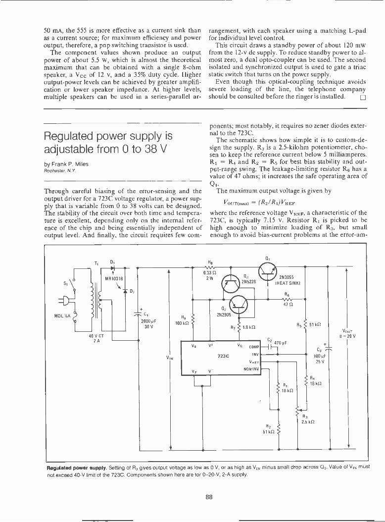
50 mA, the 555 is more effective as a current sink thanas a current source; for maximum efficiency and poweroutput, therefore, a pnp switching transistor is used.
The component values shown produce an outputpower of about 5.5 w, which is almost the theoreticalmaximum that can be obtained with a single 8 -ohmspeaker, a Vcc of 12 v, and a 35% duty cycle. Higheroutput -power levels can be achieved by greater amplifi-cation or lower speaker impedance. At higher levels,multiple speakers can be used in a series -parallel ar-
rangement, with each speaker using a matching L -padfor individual level control.
This circuit draws a standby power of about 120 mwfrom the 12-v dc supply. To reduce standby power to al-most zero, a dual opto-coupler can be used. The secondisolated and synchronized output is used to gate a triacstatic switch that turns on the power supply.
Even though this optical -coupling technique avoidssevere loading of the line, the telephone companyshould be consulted before the ringer is installed. 0
Regulated power supply isadjustable from 0 to 38 Vby Frank P. MilesRochester, N.Y.
Through careful biasing of the error -sensing and theoutput driver for a 723C voltage regulator, a power sup-ply that is variable from 0 to 38 volts can he designed.The stability of the circuit over both time and tempera-ture is excellent, depending only on the internal refer-ence of the chip and being essentially independent ofoutput level. And finally, the circuit requires few corn-
ponents; most notably, it requires no zener diodes exter-nal to the 723C.
The schematic shows how simple it is to custom -de-sign the supply. R3 is a 2.5-kilohm potentiometer, cho-sen to keep the reference current below 5 milliamperes.R1 = R4 and R2 = R5 for best bias stability and out-put -range swing. The leakage -limiting resistor R6 has avalue of 47 ohms; it increases the safe operating area ofQ.
The maximum output voltage is given by
VocTonax) = (R2/R1) VREF
where the reference voltage VREF, a characteristic of the723C, is typically 7.15 v. Resistor R1 is picked to behigh enough to minimize loading of R3, but smallenough to avoid bias -current problems at the error -am -
MD L ,4A
R8
MR10318
\*.* 02
CI
2000 pF30 V
40 V CT2A
V N
0.33 S2
2W
R9
100 kS2
02
2N2905
1.8 kS2
vo
v -
723C
COMP
INV
VREF
NON-INV
47 .S2
C2470 pF
I
R2
51 kS2
18 k2
51 kS2
C3
100µF25 V
R4
18162
R3
2 5 kS2
VOUT
0 20 V
Regulated power supply. Setting of R3 gives output voltage as low as 0 V, or as high as V1N minus small drop across 01. Value of VIN must
not exceed 40-V limit of the 723C. Components shown here are for 0-20-V, 2-A supply.
88
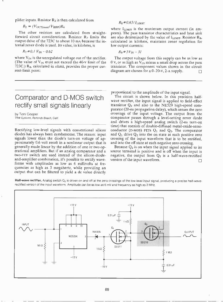
plifier inputs. Resistor R2 is then calculated from
R2 = (VOUT(max) V/ REF)R4
The other resistors are calculated from straight-forward circuit considerations. Resistor R7 limits theoutput drive of the 723C to about 10 mA because the in-ternal zener diode is used. Its value, in kilohms, is
R7 a0.1 VIN - 0.62
where VIII is the unregulated voltage out of the rectifier.(The value of VIN must not exceed the 40-v limit of the723C.) R8, calculated in ohms, provides the proper cur-rent -limit point:
R8 a 0.65//LIMIT
where ILIMIT is the maximum output current (in am-peres). The pass transistor characteristics and heat sinkare also determined by the value of 'LIMIT. Resistor R9,calculated in kilohms, maintains zener regulation forlow output currents:
Rg a 5 VIN - 31
The output voltage from this supply can be as low as0 v, or as high as VIN minus a small drop across the passtransistor. The component values shown in the circuitdiagram are chosen for a 0-20-v, 2-A supply. 0
Comparator and D-MOS switchrectify small signals linearlyby Tom CooperTRW Systems, Redondo Beach, Calif
Rectifying low-level signals with conventional silicondiodes has always been cumbersome. The reason: inputsignals lower than the diode's turn -on voltage of ap-proximately 0.6 volt result in a nonlinear output that isgenerally made linear by the addition of one or two op-erational amplifiers. But if an analog comparator and atwo-FET switch are used instead of the silicon -diode -and -amplifier combination, it's possible to rectify wave-forms with amplitudes as low as 6 millivolts at fre-quencies as high as 3 megahertz, while providing anoutput that can be filtered to yield a dc value directly
proportional to the amplitude of the input signal.The circuit is shown below. In this precision half-
wave rectifier, the input signal is applied to field-effecttransistor Q2 and also to the NE529 high-speed com-parator (20-ns propagation delay), which senses the zerocrossings of the input voltage. The output from thecomparator passes through a level -setting zener diodeand drives a high-speed analog switch (2-ns turn -ontime) that consists of double -diffused metal -oxide -semi-conductor (D-mos) FETS Qi and Q2. The comparatorand Qi drive Q2 into the on state at each positive zerocrossing of the input waveform that is to be rectified,and into the off state at each negative zero crossing.
Because Q2 is on when the input signal applied to itssource terminal is positive and is off when the input isnegative, the output from Q2 is a half -wave -rectifiedversion of the input waveform. 0
Half -wave rectifier. Analog switch 02 is driven on and off at the zero crossings of the low-level input signal, producing a precise half -wave -
rectified version of the input waveform. Amplitude can be as low as 6 mV and frequency as high as 3 MHz.
89

ICs interface keyboardto microprocessorby Donald P. Martin and Kerry S. BerlandMartin Research Ltd., Chicago, III.
A compact, economical interface between a keyboardand a microprocessor can be designed with only threeintegrated -circuit chips. The ics are a 5740 mos scan-ning keyboard encode, a 2812 mos first-in/first-out(FIFO) memory, and a 74125 quad three -state buffer. Allthree can be mounted with the standard array of key -switches and diodes on a single circuit board.
The 5740 keyboard encoder has 10 scan inputs andnine scan outputs. A unique combination of one inputand one output is assigned to each key, adding up to 90keys in all. The keys are wired between the scan inputsand the outputs with a diode in series, as shown in thecircuit diagram. The diodes block sneak signal pathsand eliminate "phantom key" effects if several keys arepressed at the same instant.
Internal ring counters simultaneously scan both thekey matrix and an internal read-only memory. When akey is pressed, the ROM word corresponding to that keyis transferred into a one -character nine -bit output latch.
The word includes the seven -bit ASCII code for the char-acter, parity bit B8 (which is not used in this design),and the selective repeat bit B9. The 5740 requires an ex-ternal clock oscillator in the 10 -to -200 -kilohertz range todrive the scanning counters; this can be obtained fromthe main timing circuit of the microprocessor.
The internal circuitry of the encoder also performsother necessary functions; it suppresses keybounce ef-fects, responds to key closures even if the previous keyhas not yet been released, and senses the shift, shift lockand control mode keys.
When the encoder recognizes a keystroke, it sets .itsdata strobe output high. This terminal is wired directlyto the encoder's data strobe control, an input terminalthat resets the encoder output on the next falling edgeof the keyboard clock. The data word is thus availableat the encoder for only one clock period.
If no more data storage were provided than the onecharacter stored by the encoder, the microprocessorwould have to test for new keyboard data at a rapidrate. This requirement would be a severe constraint onthe software, so the 2812 FIFO is included in the inter-face to provide storage of up to 32 characters.
The keystroke that sets the encoder data strobe highalso strobes the parallel load (EL) input of the FIFO andloads the ASCII character into the FIFO. The loadedcharacter moves down through the 32 positions until iteither reaches the output or is stopped by a previously
KEYBOARDCLOCK
200 pF
17 2
-12V +5V
18 32
3
10 kHz -200 kHz
+5 VCONTROLKEY
SHIFTLOCKKEY
0
019
1501sz
SHIFT 2,KEY
01501
20
CURRENTLIMITEDLEO
12
kS2
18
ki-24
-12
JSHIFT LOCKINDICATOR
CLOCK
OUTPUTENABLE
CONTROL
SHIFT
SHIFT LOCK
KEYBOUNCEMASKCONTROL
SCAN OUTPUTSXl X2 X9
VLL VGA SS
SCANNINGKEYBOARDENCODER
5740
REPEAT B9
PARITY B8
B7
86
85
B4
83
82
B1
DATASTROBE
SCAN INPUTS CNTRLY1 Y2 Y9 Y10
+5 V
2
DATA INPUT STROBEFROM MICROPROCESSOR
39
36 20-35 21
34
33 23
40 26
38 28
37
3 18
14
4 23 24 31 22
07
06
05
D4
D3
D2
01
00
PL
OE PO V,,
FIFO
2812
07
06
05
04
03
02
01
00
OUTPUTREADY
IR MR VGG SL SO V.0
250
4
TYPICALKEYSWITCHCONNECTION
INPUT READY
MASTER RESET
2
-12 V
7 6
OTHERTHREESTATE
DEVICES
CC
N87
N86
NB5
NB4
10 NB3
N82
NB1
NBO
74125
3
6 +5V1
10 kS2
-cri;REPEAT +5VKEY
10 kS2
+5V
10 k1-2
-00".-0
STATUS INPUT STROBEFROM MICROPROCESSOR
Interface. Three ICs connect keyboard to microprocessor. Encoder provides up to 90 keys. FIFO stores 32 characters. Connections tomicroprocessor are made through three -state devices to the same 8 bus lines as used by other data sources. All three ICs can be mountedwith keyswitches and diodes on a single circuit board, so when keyboard is not included in system, neither are interface components.
90
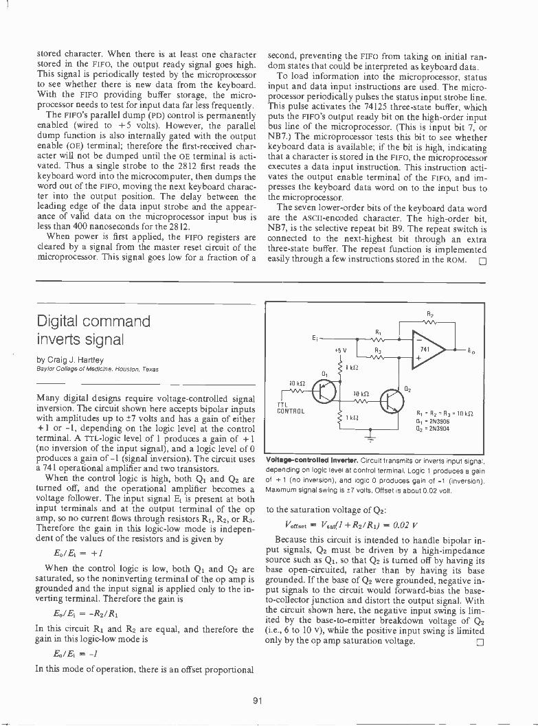
stored character. When there is at least one characterstored in the FIFO, the output ready signal goes high.This signal is periodically tested by the microprocessorto see whether there is new data from the keyboard.With the FIFO providing buffer storage, the micro-processor needs to test for input data far less frequently.
The FIFO's parallel dump (PD) control is permanentlyenabled (wired to + 5 volts). However, the paralleldump function is also internally gated with the outputenable (0E) terminal; therefore the first -received char-acter will not be dumped until the OE terminal is acti-vated. Thus a single strobe to the 2812 first reads thekeyboard word into the microcomputer, then dumps theword out of the FIFO, moving the next keyboard charac-ter into the output position. The delay between theleading edge of the data input strobe and the appear-ance of valid data on the microprocessor input bus isless than 400 nanoseconds for the 2812.
When power is first applied, the FIFO registers arecleared by a signal from the master reset circuit of themicroprocessor. This signal goes low for a fraction of a
second, preventing the FIFO from taking on initial ran-dom states that could be interpreted as keyboard data.
To load information into the microprocessor, statusinput and data input instructions are used. The micro-processor periodically pulses the status input strobe line.This pulse activates the 74125 three -state buffer, whichputs the FIFO's output ready bit on the high -order inputbus line of the microprocessor. (This is input bit 7, orNB7.) The microprocessor tests this bit to see whetherkeyboard data is available; if the bit is high, indicatingthat a character is stored in the FIFO, the microprocessorexecutes a data input instruction. This instruction acti-vates the output enable terminal of the FIFO, and im-presses the keyboard data word on to the input bus tothe microprocessor.
The seven lower -order bits of the keyboard data wordare the ASCII -encoded character. The high -order bit,NB7, is the selective repeat bit B9. The repeat switch isconnected to the next -highest bit through an extrathree -state buffer. The repeat function is implementedeasily through a few instructions stored in the ROM.
Digital commandinverts signalby Craig J. HartleyBaylor College of Medicine. Houston. Texas
Many digital designs require voltage -controlled signalinversion. The circuit shown here accepts bipolar inputswith amplitudes up to ±7 volts and has a gain of either+ 1 or -1, depending on the logic level at the controlterminal. A TTL-logic level of 1 produces a gain of +1(no inversion of the input signal), and a logic level of 0produces a gain of -1 (signal inversion). The circuit usesa 741 operational amplifier and two transistors.
When the control logic is high, both Qi and Q2 areturned off, and the operational amplifier becomes avoltage follower. The input signal E1 is present at bothinput terminals and at the output terminal of the opamp, so no current flows through resistors R1, R2, or R3.Therefore the gain in this logic -low mode is indepen-dent of the values of the resistors and is given by
Ec,/ = +1When the control logic is low, both Qi and Q2 are
saturated, so the noninverting terminal of the op amp isgrounded and the input signal is applied only to the in-verting terminal. Therefore the gain is
Eo/E, = -R2/Ri
In this circuit Ri and R2 are equal, and therefore thegain in this logic -low mode is
E0/Ei = -1
In this mode of operation, there is an offset proportional
R1 = R2 = R3 = 10 kS2,
= 2N390603 = 2N3904
Voltage -controlled Inverter. Circuit transmits or inverts input signal,depending on logic level at control terminal. Logic 1 produces a gainof + 1 (no inversion), and logic 0 produces gain of -1 (inversion).Maximum signal swing is ±7 volts. Offset is about 0.02 volt.
to the saturation voltage of Q2:
Voffset = Vsat(1 +R2/R1) = 0.02 v
Because this circuit is intended to handle bipolar in-put signals, Q2 must be driven by a high -impedancesource such as Qi, so that Q2 is turned off by having itsbase open -circuited, rather than by having its basegrounded. If the base of Q2 were grounded, negative in-put signals to the circuit would forward -bias the base -to -collector junction and distort the output signal. Withthe circuit shown here, the negative input swing is lim-ited by the base -to -emitter breakdown voltage of Q2(i.e., 6 to 10 v), while the positive input swing is limitedonly by the op amp saturation voltage.
91

Silent timer warnsof tape run -outby Vernon R. ClarkApplied Automation Inc., Bartlesville, Okla.
At concerts and lectures especially, a cassette tape oftenruns out unnoticed. One solution is to install timing cir-cuitry in the cassette -recorder case that will cause a lightto flash when it's time to reverse or replace a cassette orto switch to another recorder. This silent warning sys-tem is also useful in duplicating cassette masters, wherea preset recording time is important.
The alarm circuit operates from any voltage in the 5 -to -l5 -volt range and can either be connected to therecorder bus or use its own battery. When the circuit isturned on, a light -emitting diode begins to blink once ortwice per second, indicating that the circuit is functionaland ready to start timing. When the start -timing buttonis pushed, the LED stops flashing and stays off for theduration of the timing period. At the end of the timingperiod, the LED begins to flash again, giving the signalto flip the tape.
The two main components of the circuit are a 14536programable-timer integrated circuit and a 74C00 quadNAND gate lc. The timer contains an oscillator and a 24 -stage counter. It counts pulses from the oscillator and,when some specified counter stage goes high, delivers apositive output pulse from the decode -out terminal (pin13). Which of the counter stages triggers the output is
specified by the voltages on pins 9, 10, 11, and 12. Ifthese pins are high, high, low, and low, respectively(logic 1100), an output appears every time that stage 12of the counter goes high. With all four pins high (logic1111), output appears when stage 24 goes high.
Since this system was designed for a standard C90cassette, which runs for 45 minutes a side, the timer isadjusted to provide a timing period of 44 minutes, or2,640 seconds.Therefore the oscillator frequency is set at
foes = 223/2,640 = 3.2 kilohertz
so that counting stage 24 will go high 44 minutes afterthe counter starts counting pulses from the oscillator(provided the decoder logic is 1111).
With this oscillator frequency, if the decoder termi-nals are set at logic 1100, stage 12 goes high after 2"pulses, or
211/3.2 kHz = 0.65 second
The oscillation frequency is set by the time constantof C1 and (Ri + R2). A frequency meter is connected topin 5, and R2 is adjusted till the meter shows 3.2 kHz.
The circuit operates as follows: while the on -offswitch is off, all pins are low. When the switch is turnedon, pins 9 and 10 of the timer go high because they arewired to the positive -voltage bus. Therefore the decoderis programed with logic 1100, and the LED begins toflash every 0.65 second. When the start -timing button ispushed, the quad NAND circuit sets the decoder to logic1111, so the LED stops flashing and the 44 -minute countbegins. After 44 minutes, the decode -out terminal (pin13) goes high, resetting the decoder to 1100 so that thealarm signal flashes again.
OFF
9V
0ON
OSCINH
START TIMING \ 102
-CLK INH 7- RESET SET
1+F
1 MS2
8 BYPASS
+9 V BUS
14
200 kS2
IN
OSCILLATOR
6
STAGES1 THROUGH 8
14536
CND" OUT 1
20
0UT:s
131 120 k1.20.001,../F
C,T
74C00
STAGES 9 THROUGH 24
9 10 11 12 13 In 15 I.:17 18 19 20 21 22 2 3 24
I I I I 1 I I I I I I I I
12
c
10
9V
9
DECODER
15
MONOSTABLEMULTIVIBRATOR
13DECODEOUT
+9 V
1k12
2N412447 k12
A MONO IN
101,12 FLV100
Silent warning. LED starts to flash 44 minutes after start -timing but
ton is pushed, warning that cassette tape is about to run out. Circuitis useful at concerts, lectures, and tape -duplication sessions. It canbe built into recorder case and uses either its own battery or thepower source of the recorder-it draws only a matter of 200 micro-amperes in the timing mode and 4 milliamperes in the flashing mode.
92

Antilog function generatorkeeps VCO output linearby J. A. Connelly and C. D. ThompsonGeorgia Institute of Technology, Atlanta, Ga.
Accurate voltage control of oscillator frequency is cru-cial for such applications as electronic music synthesi-zers, filter test circuits, and phase -locked loops. In thevoltage -controlled oscillator (vco) described here, each1 -volt change in the control voltage changes the outputfrequency by one octave with a maximum deviation of±0.4% over the entire audio range. This precision isachieved by temperature -compensation and buffering.
Circuit can be built with readily available parts, andthe design equations allow adjustability and flexibilityto meet a variety of specific needs. The total range of os-cillation frequency can be shifted down one octave, forexample, by doubling the capacitance of C1 in the vco.
This vco is basically a relaxation oscillator: currentsource Q5 charges low -leakage polystyrene capacitor C1until unijunction transistor Q4 fires (at about 9 v); Cithen discharges rapidly, and the cycle starts all overagain. The sawtooth output voltage essentially resultsfrom the voltage across C1 minus a couple of junctionvoltages, buffered by high -impedance MOSFET Q2; byQ3, which carries the current to fire Q4; and by theunity -gain op amp. Most of the resistorscurrents to safe levels.
The oscillation frequency is determined by the charg-ing current into C1. This current, which is the collectorcurrent from Q5B, depends upon the control voltage be-cause the base -to -emitter voltage VBE in both halves ofQ5 is derived from the control voltage, thus,
Ic = Alsexp(qVBE/kT)
100 pF
1 MS2
-15 V -VVV-4k-
150 1(12
CONTROLVOLTAGE
V TRIM
QIN = 109 kit
91 k5-2
2.2 k52
RTC2 1(12
0.34 %/°C
AD821
058
Voltage -controlled oscillator. Basic circuit is relaxation oscillatorbuilt around timing capacitor C1 and unijunction transistor. Antilogfunction generator (in shaded area) supplies charging current thatvaries exponentially with control voltage. Tuning curve is 1 -octave -
per -volt straight line. If RIN were 31.4 kilohms, tuning curve would beone -decade -per -volt straight line.
where $ is the short-circuit current gain, Is is the reversesaturation current, kT/q is 0.026 per volt at 27°C, andVBE is scaled from the control voltage V in a voltage-divider network:
VBE = VRTC/(RIN + RTC)
Therefore, the collector current is given as a function ofthe control voltage by
rr gRIT, VIc 1
=I3Is exP[ kT(RIN + TC,)1 = 8181<1.
In this expression, the scale factor K is just a substitu-tion that replaces several terms: that is,
K = expkT(R:RT-4-c RTC)]
Current Ic is an antilog function (or exponential func-tion) of voltage, and therefore the current source iscalled an antilog function generator.
Because the frequency is directly proportional to Ic,
f Kv = foKvwhere f0 is the free -running frequency (i.e., the oscilla-tor frequency when control voltage V is zero). The fre-quency f0 depends on the parameters of Q5, the firingvoltage of Q4, and the capacitance of Ci.
The value of scale factor K is set -by the resistors RIN
104
zw
ce 103
102
20 11111111111-6 -4 -2 0 2
CONTROL VOLTAGE (VOLTS)4 6
Q, = 2N3904 03 = 2N3904Q2 = 2N3796 04 = 2N2646
27 k52C,
390 S2
100 k12
2 2 kS2 Z 12012
15V200 pF LOW LEAKAGE POLYSTYRENE
*15V
OFFSET25 k12
OUTPUT
93

and RTc in the divider network. If K is 10, the oscilla-tion frequency changes by one decade when V changesby 1 v. With the resistance values shown in the circuitdiagram, however, K is 2, so the frequency changes byone octave when V changes by 1 v.
The temperature sensitivity of Ic is compensated bythe temperature coefficient of thermistor RTC,+0.34%/°C, which is equal in magnitude and oppositein sign to the effect of q/kT in the expression for K.
Thus, scale factor K is independent of temperature ifthe thermistor and Q5 have equal temperatures. To en-sure this condition, the thermistor is mounted in ther-mal contact with the header of Q5.
The tuning curve shows the experimental perform-ance of the vco. The maximum departure from thestraight-line relationship is only ±0.4% over the audio -frequency range from 20 Hz to 20 kHz. Outside thatrange, the voltage control becomes less precise.
Radiation monitor haslinear outputby Paul Prazak, Burr -Brown Research Corp., Tucson, Ariz.,and Lt. William B. Scott, Edwards AFB, Calif.
A commercial silicon diode can be used as a direct -reading detector of gamma rays and high-energy X raysin radiotherapy. Besides generating an output that islinearly proportional to the radiation intensity, thediode makes a small enough probe to map the radiationfield accurately. The monitoring system of diode plustwo operational amplifiers provides an output voltagethat varies linearly from 0.1 volt to 10 v as the dose ratevaries from 10 rads per minute to 1,000 rads/min.
The 1N3191 or other off -the -shelf diode is operatedin a zero -bias short-circuit mode. Irradiation of thediode junction creates electrons and holes that are col-lected by the depletion gradient, producing a nanoam-pere current which is proportional to the intensity of theradiation.
To amplify the small signal from the diode, a 3521Loperational amplifier with low bias current (10 picoam-peres maximum) and ultra -low offset voltage drift (±1microvolt/°C maximum) is used. As shown in Fig. 1,
the 3521L is connected in a current -to -voltage configu-ration where the inverting input appears as a virtual
ground. This FET-input op amp delivers output voltagesof 100 'iv to 10 millivolts, which are well above thenoise level. The 200-kilohm resistor between groundand the noninverting input serves to balance the ampli-fier, and the 0.1-microfarad capacitor stabilizes the am-plifier by shunting out noise and preventing oscillationsresulting from positive feedback.
An additional stage of gain amplifies the signal to thedesired level. The offset -voltage drift of this stage mustbe extremely low because it is amplified along with thesignal. Therefore the chopper -stabilized 3292 op amp,which has a maximum offset drift of only ±0.3 µv/°C isused here. The 100 -ohm resistor again balances the in-puts to the amplifier. The gain of this stage should bearound 1,000; it is adjusted by means of the 20 -ohm po-tentiometer so that an output voltage of 0.10 v to 10.00v corresponds to a dose rate of 10 rads/min to 1,000rads/min at the detector, as shown in Fig. 2.
The output voltage can be displayed on a 31/2 -digitpanel meter, so that the numerals directly indicate radi-ation intensity. An alternative is to use an ultralinearvoltage -to -frequency converter, an optical coupler, acounter, and a display to completely isolate the radio-therapy patient from the monitoring and recording sys-tem. An advantage of this approach is that the integrat-ing input of the voltage/frequency converter wouldaverage out any high -frequency noise in the system. El
EARTHGROUND
1N3151
200 kV,
-15V
0.1 pF
100 kS2
100 S220 S2
3292GAINADJUST
100 12
15V
V01,1
1. Dosage -rate meter. Commercial diode is detector in this highly accurate radiation moni-tor. Low -drift FET-input op amp amplifies detector current to usable level, and chopper -stabi-lized amplifier then provides additional gain while minimizing any error caused by ambient -temperature fluctuations. Gain is adjusted so that output voltage is 1% of incident radiationintensity in rads per minute; therefore voltage can be displayed on 3Y2 -digit DVM for directreading of dosage rate. Cost of parts for this monitor is about $90.
10
8
60
40
2
0 200 400 600 800 1000
DOSE RATE (RADS/MIN)
2. Linear response. Output voltage frommonitor is linearly proportional to radiationintensity at diode. Over dosage rate rangeshown, total system error is less than 1 %.Small size of diode probe permits accuratemapping of radiation field.
94
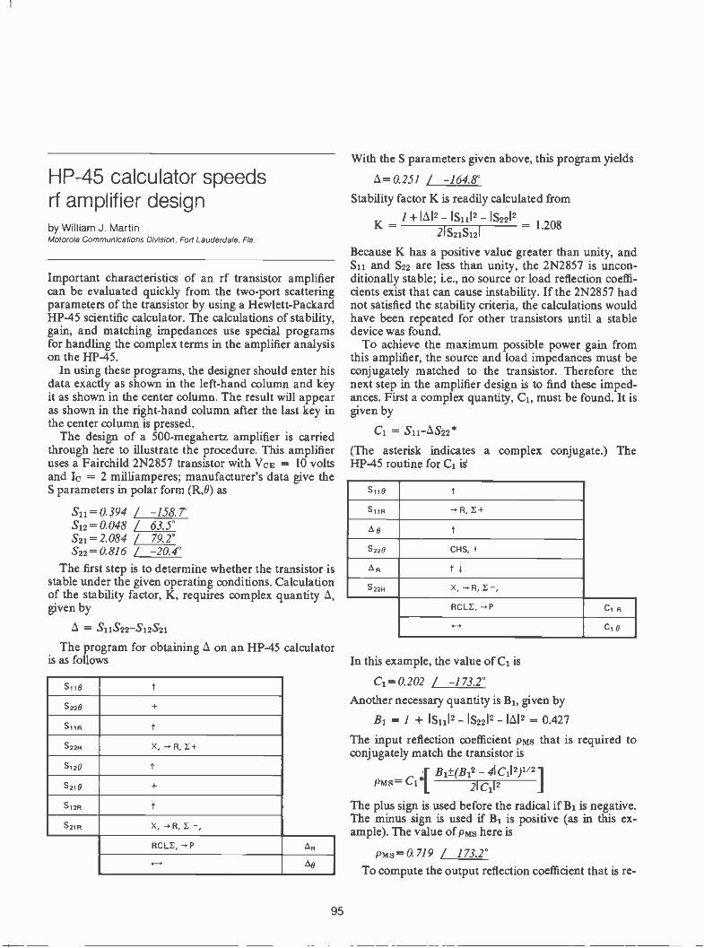
HP -45 calculator speedsrf amplifier designby William J. MartinMotorola Communications Division, Fort Lauderdale, Fla.
Important characteristics of an rf transistor amplifiercan be evaluated quickly from the two -port scatteringparameters of the transistor by using a Hewlett-PackardHP -45 scientific calculator. The calculations of stability,gain, and matching impedances use special programsfor handling the complex terms in the amplifier analysison the HP -45.
In using these programs, the designer should enter hisdata exactly as shown in the left-hand column and keyit as shown in the center column. The result will appearas shown in the right-hand column after the last key inthe center column is pressed.
The design of a 500 -megahertz amplifier is carriedthrough here to illustrate the procedure. This amplifieruses a Fairchild 2N2857 transistor with VcE = 10 voltsand Ic = 2 milliamperes; manufacturer's data give theS parameters in polar form (R,O) as
Sll = 0.394 / -158.7°S12 = 0.048 / 63.5°S21=2.084 / 79.2°S22 = 0.816 / -20.4°
The first step is to determine whether the transistor isstable under the given operating conditions. Calculationof the stability factor, K, requires complex quantity A,given by
A = S11S22-S12S21
The program for obtaining A on an HP -45 calculatoris as follows
S110 t
5220 +
S11R t
S22R X, -. R, X+
S120 t
S210 +
S12R t
S2,R X, -.R, I -,
RCLI, -°P OR
oe
With the S parameters given above, this program yields
A=0.251 -164.8°
Stability factor K is readily calculated from
1 +1Al2 -151112 - 1S2212K - = 1.20821S2iSi2i
Because K has a positive value greater than unity, andS11 and S22 are less than unity, the 2N2857 is uncon-ditionally stable; i.e., no source or load reflection coeffi-cients exist that can cause instability. If the 2N2857 hadnot satisfied the stability criteria, the calculations wouldhave been repeated for other transistors until a stabledevice was found.
To achieve the maximum possible power gain fromthis amplifier, the source and load impedances must beconjugately matched to the transistor. Therefore thenext step in the amplifier design is to find these imped-ances. First a complex quantity, C1, must be found. It isgiven by
= Sii-AS22*
(The asterisk indicates a complex conjugate.) TheHP -45 routine for C1 is'
S0S11R
9 t
S220 CHS, +
OR t1S22R X, -.R,
RCLZ, -.P C1 R
Cl
In this example, the value of Cl is
C1=0.202 / -173.2°
Another necessary quantity is B1, given by
B1 = / + 1S1112 - 1S2212 - IA12 = 0.427
The input reflection coefficient pms that is required toconjugately match the transistor is
B1 -1-(B12 - 41(.112)112PMs=C11L
21C112
The plus sign is used before the radical if B1 is negative.The minus sign is used if Bi is positive (as in this ex-ample). The value of pms here is
pms= 0.719 / 173.2°
To compute the output reflection coefficient that is re -
95

quired to conjugately match the output of the transistor,complex quantity C2 must be found.
C2 = S22-AS11*
The HP -45 routine for C2 is completely analagous tothat for Ci and yields
C2= 0.721 / -22.3°
Quantity B2 is also required. It is given by
B2 = 1 + 1S2212 - IS1112 - IA12 = 1.448
The output reflection coefficient pmL for conjugatematch to the transistor is
Pm', = C2*[B2 -±(B22 - 4I C212)112]
21C212
The plus sign is used for negative values of B2, and theminus sign for positive values of B2. Here
PmL= 0.910 / 22.3°
Reflection coefficients pms and pmi, can be converted to
Matched circuit. Source and load impedances shown producemaximum possible power gain (13.6 dB) from 2N2857 operating at500 MHz with VcE 10 volts and lc 2 milliamperes. Calculations
of impedances and gain, as well as verification of amplifier stability,require only transistor S parameters and HP -45 scientific calculator.
SOURCE
0.93 nH 8.2 12
76.2 nH 59.212
LOAD
source and load impedances, respectively, by a graph-ical method (plotting on a Smith chart) or by the follow-ing HP -45 routine, which gives polar, series, and paral-lel forms for the impedance.
Pe t
PR - R,1,+,-°P
0 t, 1, --0R, +, 1, 1
Po t
PR - R, -,
1, .1.,
CHS,1,
1,1,1, +, .--., 50, X MAG.
.--. 0
4-4. -r. R, Rs
xs
--*P, 1, 1,1, COS,
--, 50, X Rp
SIN, ±, 50, x x,
> POLAR
> SERIES
> PARALLEL
The results, in series form, for this example are
Zsource = (8.19 + j 2.91) ohmsZioad = (59.23 + j 239.15) ohms
Thus, the circuit shown in the accompanying diagramprovides maximum possible power gain from this am-plifier at the given values of frequency, voltage, andcurrent.
The final step in the design analysis is to calculate thevalue of this maximum possible power gain. It is givenin decibels as
Gm =1
g-211
K±(K2 - 1)1/21ax .75
The plus sign is used in front of the radical if B1 is nega-tive. The minus sign is used if B1 is positive, In this ex-ample the minus sign is used, and
G. = 13.6 dBfor a Fairchild 2N2857 transistor operated at 500 MHzwith VcE = 10 v and Ic = 2 mA.
This brief presentation has shown HP -45 routines foronly the complex quantities A, Ci, and Z. Routines inthe same format for the other quantities discussed (K,B1, B2, Pmg, and pmL) are available from the author.Also available are routines for pms' and piga:. Quantitypms' gives the complex source impedance once the com-plex output impedance is known (from constant gaincircles if a power gain other than G. is desired).Quantity pm1,' gives the complex output impedanceonce the complex input impedance is known (e.g., forbest noise match). 0
96

Waveform is synthesizedfrom linear segmentsby E. D. UrbanekBell Telephone Laboratories, Murray Hill, N.J.
Just as a curve can be approximated by a series ofstraight lines, so can a waveform be approximated by asuccession of voltage ramps. The voltage ramps may bethe output of an integrator driven by a succession ofrectangular pulses of various amplitudes and durations.Figure 1 shows how the integration of three such pulsesproduces three sequential ramps to yield a novel waveshape. The amplitude and polarity of each pulse deter-mine the slope and direction of the correspondingramp, and the width of the pulse determines the lengthof the ramp. The output voltage function can be madeto resemble a curve if enough pulses and ramp seg-ments are used.
A function generator that synthesizes waveforms inthis manner is used as a control for automatic -gain -con-trol circuits and for sweep generation. As shown in Fig.2, it contains type 121 one-shot multivibrators to gener-ate the pulses that are to be integrated, a 741 oper-ational amplifier connected as an inverter to change thepolarity of pulses when necessary, and another 741 opamp connected as an integrator. The 2N2481 transistorprevents drift.
The one-shot units are arranged in a series so that thecomplementary output (Q) of the first unit serves as the
1. Waveform generation. Integration of sequential rectangularpulses produces sequential voltage ramps that make up outputwaveform. Amplitude, polarity, and duration of pulses determine theslope, direction, and length of the ramps.
trigger for the second unit, and so forth. This arrange-ment produces a sequence of positive pulses. The dura-tion of each pulse is determined by the timing resistorand capacitor of its one-shot, and the amplitude of eachpulse is set by the potentiometer at the output of theone-shot. Each positive pulse can be connected directlyto the integrator to produce a ramp with negative slope,or it can be connected through the inverter and thenceto the integrator to produce a ramp with positive slope.
10
121
9 470 11
1µF
10 QX vvs.
+5 V2N2481
0.1µF10
JL 100 kit 1001(125 121 5 VIA Mti
STARTING 9
10 kitPULSE
+5 V 100 kit
741 100MA
0 1 ;IF
I I-4°0.1 -JE10
02;IF
5 kS2
INVERTER
5 121
9 100 k1210 kit E2 -
741+5 V INTEGRATOR
0.1 AF10
031
5 1219
5k52
10 kit
+5 V
2. Circuit. Function generator uses one-shot multivibrators to supply series of pulses to op amp connected as integrator. Pulse polarity canbe reversed by op amp connected as inverter. Complementary output from each pulse generator triggers next pulse in sequence, producingcontinuity in wave shape. Pulse widths are set by RC time constant for each one-shot, and pulse amplitudes are set by potentiometers.
97

3. Waveforms. Scope traces generated by seven -segment function generator. Maximum voltage on these traces is about 0.5 volt, and dura-
tion of traces is about 4 milliseconds. Traces could be brought down to zero -voltage level smoothly, by sloping segments, or abruptly, by use
of transistor to short-circuit integrating capacitor. Trace on right here shows that just a few segments suffice to approximate a curve.
An additional one-shot unit and the transistor areused to form an anti -drift control. The complementaryoutput (Q) of this one-shot is used to drive the transis-tor, which discharges the 0.1-microfarad integrating ca-pacitor. With no input pulse applied, the transistorkeeps the capacitor discharged. Holding the integratoroutput at zero in this way prevents integration of anyoffset voltages. When an input pulse is applied to startthe function generator, (Q) is driven off and the tran-sistor releases the capacitor. The off time of (Q) may beadjusted to coincide with the total on time of the func-tion generator, or it may be adjusted to terminate thewaveform at any point during the on time.
Scope traces of seven -segment waveforms are shownin Fig. 3. The voltage level remains constant (becausethere is no input pulse to the integrator) between theend of the seventh segment and the retriggering of thestart pulse. The maximum voltage on each trace is
about 0.5 volt, and the total duration of a trace is about4 milliseconds.
In applications where a wide range of ramp slope isrequired, the potentiometer attenuators can be elimi-nated, and the input resistors on the inverter and in-tegrator can be made variable. This increases invertergain and allows control of both voltage and time con-stant of the integrator for adjusting the slopes.
Direct -reading converteryields temperatureby James Williams and Thomas DurgavichMassachusetts Institute of Technology, Cambridge, Mass.
It's possible to convert temperature accurately to a nu-merically equivalent frequency for direct display or forinstrumentation. The circuit described here uses an1N914 temperature -sensing diode to provide 0.1°C res-olution from 0°C to 100°C, with accuracy of ±0.3°C overthe entire range.
The 301A operational amplifier is set up as an in-tegrator. The 150-picofarad capacitor from the invertinginput to pin 1 provides feed -forward compensation forhigh slew rate. The 2N2646 unijunction transistor resetsthe integrator when the 4300-pF capacitor charges toabout -10 volts. The 1N821 temperature -compensateddiode provides a voltage reference that determines thefiring point of the unijunction transistor, provides stablezero and full-scale references, and sends a 1 -milliam-
pere current through the 1N914 temperature -sensingdiode. The 2N2222 transistor and its associated compo-nents provide an output pulse that is compatible withtransistor -transistor logic.
In operation, the circuit functions as a voltage -to -fre-quency converter. The voltage at the wiper arm of the1-kilohm potentiometer is integrated until the transis-tor's firing point is reached. When the transistor fires, itresets the capacitor. The frequency of oscillation is re-lated to temperature because the diode voltage biasesthe integrator via the noninverting input. The only vari-able voltage available to the amplifier is the tempera-ture -dependent (-2.2 millivolts per °C) potential fromthe 1N914 diode. To adjust the circuit, put the diode ina 100°C environment and turn the 10-kilohm poten-tiometer till the output frequency is 1,000 hertz. Thenput the diode in a 0°C environment, and turn the1-kilohm potentiometer for 0 Hz out. This proceduremust be repeated two or three times, until the adjust-ments cease to interact. Once the circuit is adjusted, itsoutput frequency is 10 times the sensed temperaturewithin 0.3°C from 0° to 100°C. For example, if the tem-perature is 37.5°C, the meter will read 375 Hz.
The output frequency can be counted by TTL count -
98

+15 V
866 El1k12
1N821(6.2 V1
8.06 kE2
2N2646
tip4300 pF
+15 V
10 162
11(1-2
ZEROADJUST
10 kE2
150 pF
301
+15 V5V
5 ps
2N2222680 pF
OUTPUT0
4.7 kE2
2.2 kE2
FULL-SCALEADJUST 2.21(2
-15 V2.2 kfl
4.7 k.S2 5% TOLERANCE6.19 kE2 10 kE2
1N914
TEMPERATURE - 86612SENSING DIODE 1 kE2
6.19 kE2FILM TYPE,1% TOLERANCE
8.06 1(2
Temperature -to -frequency converter. Frequency of relaxation oscillator varies with temperature -dependent voltage across 1N914 diode.Over 0°C -to -100°C temperature range, frequency changes linearly from 0 to 1,000 Hz. Therefore frequency meter at output can show tem-perature directly. Accuracy is ±0.3°C. Excellent performance and low cost (less than $5 for parts) make this circuit outstanding.
ers and a 1 -Hz square wave. The 1 -Hz square wave canbe fed to the base of the 2N2222 through a 2.2-kilohm
resistor, and the resultant gated pulses at the output canthen be fed to TTL counters. 0
One NOR gate startsshift -register loopby Jean-Pierre DujardinOhio State University, Columbus, Ohio
A circulating shift register with a single logic 1 in theloop is required in cyclic -triggering operations such assampling transducers in time-sharing telemetry. Sys-tems for starting this type of circuit are often complex,but the arrangement shown here simply uses a NOR gatewith the four -stage shift register.
As the waveforms show, the output terminals of the4015A shift register go high in a continuing sequencefrom stage one through stage four and then back tostage one again. The 4002A three -input NOR gate startsthis operation and keeps it going.
The input terminals of the NOR gate are connected tothe first three output terminals of the shift register.When these terminals are at logic 0, the output terminalof the gate is at logic 1, which is bro,: grit to the data in-put terminal (D) of the register. Ti next clock pulsetransfers the logic 1 at D into the first stage of the regis-ter. When at least one of the inputs to the gate is a logic1, the output from the gate is a 0, which is presented tothe register input. Thus, after a maximum of three clockpulses, a single 1 is circulating.
This circuit requires no external timing to introduce
the single 1 into the loop and no resetting. If externalnoise introduces errors, they are automatically cor-rected. Extension of the system to more than four shift -register stages is straightforward: outputs from all butthe last stage are fed into a NOR gate that, in turn, feedsthe D input of the first stage in the register.
C-MOS ring circuit. Arrangement of NOR gate and four -stage shiftregister provides a pulse output that circulates to each of the outputterminals in sequence, moving from one stage to the next as theclock cycles. The two C-MOS ICs determine performance level.
99
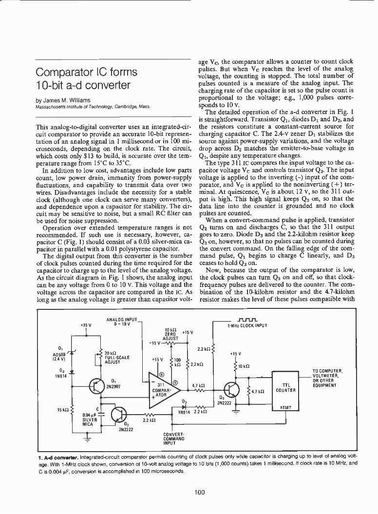
Comparator IC forms10 -bit a -d converterby James M. WilliamsMassachusetts Institute of Technology, Cambridge, Mass.
This analog -to -digital converter uses an integrated -cir-cuit comparator to provide an accurate 10 -bit represen-tation of an analog signal in 1 millisecond or in 100 mi-croseconds, depending on the clock rate. The circuit,which costs only $13 to build, is accurate over the tem-perature range from 15°C to 35°C.
In addition to low cost, advantages include low partscount, low power drain, immunity from power -supplyfluctuations, and capability to transmit data over twowires. Disadvantages include the necessity for a stableclock (although one clock can serve many converters),and dependence upon a capacitor for stability. The cir-cuit may be sensitive to noise, but a small RC filter canbe used for noise suppression.
Operation over extended temperature ranges is notrecommended. If such use is necessary, however, ca-pacitor C (Fig. 1) should consist of a 0.03 silver -mica ca-pacitor in parallel with a 0.01 polystyrene capacitor.
The digital output from this converter is the numberof clock pulses counted during the time required for thecapacitor to charge up to the level of the analog voltage.As the circuit diagram in Fig. 1 shows, the analog inputcan be any voltage from 0 to 10 v. This voltage and thevoltage across the capacitor are compared in the Ic. Aslong as the analog voltage is greater than capacitor volt-
age Vc, the comparator allows a counter to count clockpulses. But when Vc reaches the level of the analogvoltage, the counting is stopped. The total number ofpulses counted is a measure of the analog input. Thecharging rate of the capacitor is set so the pulse count isproportional to the voltage; e.g., 1,000 pulses corre-sponds to 10 v.
The detailed operation of the a -d converter in Fig. 1is straightforward. Transistor Qi, diodes D1 and D2, andthe resistors constitute a constant -current source forcharging capacitor C. The 2.4-v zener D1 stabilizes thesource against power -supply variations, and the voltagedrop across D2 matches the emitter -to -base voltage inQi, despite any temperature changes.
The type 311 Ic compares the input voltage to the ca-pacitor voltage Vc and controls transistor Q3. The inputvoltage is applied to the inverting (-) input of the com-parator, and Vc is applied to the noninverting ( +) ter-minal. At quiescence, Vc is about 12 v, so the 311 out-put is high. This high signal keeps Q3 on, so that thedata line into the counter is grounded and no clockpulses are counted.
When a convert -command pulse is applied, transistorQ2 turns on and discharges C, so that the 311 outputgoes to zero. Diode D3 and the 2.2-kilohm resistor keepQ3 on, however, so that no pulses can be counted duringthe convert command. On the falling edge of the com-mand pulse, Qi begins to charge C linearly, and D3ceases to hold Q3 on.
Now, because the output of the comparator is low,the clock pulses can turn Q3 on and off, so that clock -frequency pulses are delivered to the counter. The com-bination of the 10-kilohm resistor and the 4.7-kilohtnresistor makes the level of these pulses compatible with
01
AD580(2.4 VI
021N914
151(0
+15 V
1
ANALOG INPUT_0 - 10 V
20 kS2FULL-SCALEADJUST
a,2N2907
10 kSZZERO +15 V
ADJUST-15 V
2.2 kSZ
+15 V 100kS2 2.2 kSZ
0.04µFSI LVERMICA Il (12
2N2222
4-
311 4.7k2COMPAR-
ATOR
2.2 kS2
D3
1N914 2.2 1St
_11.11.11_1 -MHz CLOCK INPUT
+15 V
10 k12TO COMPUTER,VOLTMETER,OR OTHER
da,TTL EQUIPMENT
Q3
4.7 Icfl COUNTER
2N2222RESET
CONVERT -COMMANDINPUT
1. A -d convertor. Integrated -circuit comparator permits counting of clock pulses only while capacitor is charging up to level ofanalog volt-
age. With 1 -MHz clock shown, conversion of 10 -volt analog voltage to 10 bits (1,000 counts) takes 1 millisecond. If clock rate is 10 MHz, and
C is 0.004 µF, conversion is accomplished in 100 microseconds.
100

ri[4-CONVERT- 512s
COMMAND0 I IPULSE
12 V
ANALOGVC VOLTAGE
121
COMPARATOROUTPUT
PULSES TO1 -MHz 5 V -
COUNTER
0
L
VON Q :i1110 OIL650 PULSES
2. Timing diagram. For an analog voltage of 6.5 V as in this ex-ample, 650 pulses are counted while capacitor charges up to turnoff comparator output. Convert commands can be given at any rateup to 1 kHz for circuit as shown in Fig. 1.
transistor -transistor logic (m) in the counter circuit.When Vc charges up to the level of the input voltage,
the 311 output goes high again, which turns on Q3 andgrounds the data line so that no more pulses arecounted. Fig. 2 shows the timing diagram for the con-verter operation.
To calibrate the counter, a 10-v signal is applied atthe input, and the 20-kilohm potentiometer is adjustedso that 1,000 pulses appear at the counter for each con-version command. Then a 0.01-v signal is applied, andthe 10-kilohm pot is adjusted so that 1 pulse is countedfor each conversion. The unorthodox voltage -offset ad-justment for the comparator corrects for incomplete dis-charge of C; the minimum voltage across C is VcE(sat)of Q2.
The circuit in Fig. 1 can convert 10 bits (i.e., count1,000 pulses) in 1 ms. For conversion in 100 ps, the clockfrequency must be 10 megahertz, and C must be 0.004microfarad. Conversion commands can then be given atrates up to 10 kilohertz. 0
Overrange indicator canenhance frequency meterby F. E. HinkleThe Applied Research Laboratories, University of Texas, Austin, Texas
By making use of a 556 integrated circuit, which is com-posed of two 555 timers in a single package, an over -
range indicator can be economically added to an analogfrequency meter. A 555 can be used alone as a mono-
stable multivibrator that is triggered by the frequencyto be measured. To provide unambiguous measure-ments, however, the meter described here uses a secondtimer to flash a warning light whenever the input ex-ceeds the maximum frequency setting. Although thetechnique of using monostables in analog frequencymeters is not new, the use of new circuit developmentsmakes the design economical and easy to implement.
When the range switch on this meter is set to the 50 -hertz range, any input frequency from near dc to 50 Hzcauses a panel meter to read correctly; e.g., a frequencyof 42 Hz produces a meter reading of 42 microamperes.However, the meter reading is incorrect when the input
15 pFsov-n-n- -11 tAs
INPUT 1 kS2
1N914
+9 V
1 ks2
2N4401
10 :-kS2
14
%5562
3
4.7k0231.5 kS210 kS2
Q2
2N4403
10.01'ALF
1 C1I0.01pF' 47 Id/
9
%556 12
13
10 11
'Oft
1 MS2
=0.01µF
R2
0.01 pF C2
FREQUENCY RANGE50 Hz 500 Hz 5 kHz 50 kHz
M121
kS2 1
Id/
100 / 10
RANGESWITCH
180 kn
50-µAtl 10 vvPF PANELMETER
220 52sro.
MONSANTO 1 41LEDMV 50
TIMINGRESISTORS
RI
FREQUENCYREADOUT
OVER RANGEINDICATOR
Unambiguous. Addition of overrange indicator to analog frequency meter warns when switch Is set to wrong frequency range. Transistor Cizallows input signal to trigger LED monostable whenever input frequency is greater than meter range. Inexpensive and reliable circuit shown isuseful from near dc to well over 20 kHz.
101

frequency exceeds 50 Hz, and therefore a light -emitting -diode overrange indicator flashes. If the range switch isthen moved to a setting higher than the frequency, theLED stops flashing and the meter again indicates cor-rectly. For example, a 300 -Hz signal would be measuredon the 500 -Hz range, and the meter would show 30 mi-croamperes.
In the meter diagramed here, the upper portion of thecircuit measures the frequency and has the 50-µA panelmeter as its readout. The lower portion provides theoverrange indication and has the LED as its warninglight. These two portions of the circuit are driven by acommon input.
The input signal is a rectangular pulse train; thepulses are differentiated to produce the negative spikesthat are needed to trigger the timer. For a sine -wave orsawtooth input signal, a Schmitt trigger might be usedto generate the negative impulses.
When pin 6 of the frequency -measurement mono -stable is triggered, pin 5 goes high. It stays high and de-livers current for a time equal to 1.1111CI. This positiveoutput pulse appears once for every cycle of the inputfrequency (unless the trigger impulse arrives while the
output at pin 5 is already high). The current pulses,smoothed by the 10-microfarad capacitor, provide anaverage value that is shown on the microammeter.
At low frequencies, the output pulses are well sepa-rated, so the average current is low. At higher fre-quencies, however, they are closely spaced and ap-proach a duty factor of about 95% at the upperfrequency limit set by the range switch. Average currentthus increases as the frequency increases. Resistors inthe output circuit are chosen so that the average currentis 50 µA at the maximum frequency in each range.
If the input frequency exceeds the meter range, a trig-ger spike arrives while the output is already high. As aresult, that input cycle is not counted, so the frequencymeter indication is erroneous.
To warn that trigger impulses are arriving while pin 5is high, pin 5 is also connected to the base of pnp tran-sistor Q2. When pin 5 is low, Q2 conducts and holds pin8 high, thus preventing She warning -indicator mono-stable from being triggered. But when pin 5 is high, Q2is turned off; a negative input spike that reaches pin 8therefore can trigger an output from pin 9 that flashesthe LED. The duration of the flash is 1.1R2C2.
Pulse -frequency doublerrequires no adjustmentby Thomas McGaheeDon Bosco Technical High School, Boston, Mass.
Sometimes a frequency doubler is needed in a digitalsystem, and unfortunately most doubler circuits have tobe adjusted for a particular operating frequency. How-ever, this circuit, which has operated successfully in aspeciallyidesigned divide -by -N counter, requires no ad-justment over a range from near dc to 10 megahertz.
When a signal pulse passes through the circuit, eachinverter introduces a small delay, typically of 20nanoseconds, in addition to inverting the pulse. For ex-ample, the signal at point D inverts 60 ns after the inputsignal at point A has inverted; thus, gate 6 continues tohave high signals at both of its input terminals for 60 nsafter the input at point A changes from low to high. Asa result, the output from gate 6 (i.e., point F) will go lowfor 60 ns after a positive -going transition at the input tothe circuit.
Somewhat the same thing occurs at gate 5, exceptthat it develops a 60-ns low output after a negative -go-ing transition at the input. In the circuit diagram, inver-ters 1, 2, and 3 all serve double duty in producing these60-ns low pulses at points F and G. This design reducesthe number of gates needed.
The pulses from gates 5 and 6 are fed to the terminalsof gate 7, which produces a positive pulse 60 ns wide ev-ery time either one of its input terminals goes low. Sinceone terminal goes low on the leading edge of each inputpulse at point A, and the other terminal goes low on thetrailing edge of each input pulse at A, the frequency of
the output pulses at point H is twice the frequency ofthe input pulses at point A.
The output is in the form of positive pulses that are60 ns wide. There is a 20-ns difference in the spacing be-tween successive output pulses because the portion ofthe circuit that comprises the negative -going edge -de-tector has one more inverter stage than the positive -go-ing edge -detector section does. This slight asymmetry isnoticeable only at the highest frequencies. If partic-ularly slow input signals are used, it is a good idea toplace a Schmitt trigger just before the input. 0
(INPUT)
VOLTAGEAT
A
B
F
H
5V
0
5VL0
H
(OUTPUT)
2 3 4
INVERTERS ARE TYPE 7404, NAND GATES ARE TYPE 7400
5V h10 1
5V
0
5v r
I
5Vr0
5Vr0
5 V r
3 GATE DELAYS TIME
Frequency doubler. Propagation delays through inverters causeNAND gates 5 and 6 to go low for 60 nanoseconds following the ris-ing and falling edges, respectively, of input pulse. Therefore outputgoes high twice as often as input.
102
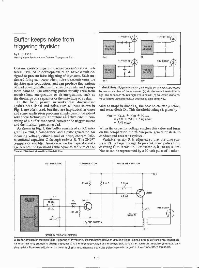
Buffer keeps noise fromtriggering thyristorby L. R. RiceWestinghouse Semiconductor Division, Youngwood, Pa.'
Certain shortcomings in passive noise -rejection net-works have led to development of an active circuit de-signed to prevent false triggering of thyristors. Such un-desired firing can occur when noise transients cross thethyristor gate conductors, and can produce fluctuationsof load power, oscillations in control circuits, and equip-ment damage. The offending pulses usually arise fromreactive -load energization or de-energization, such asthe discharge of a capacitor or the switching of a relay.
In the field, passive networks that discriminateagainst both signal and noise, such as those shown inFig. 1, are often used, but they are impractical at timesand some application problems simply cannot be solvedwith these techniques. Therefore an active circuit, con-sisting of a buffer connected between the trigger sourceand the thyristor gate, is needed.
As shown in Fig. 2, this buffer consists of an RC inte-grating circuit, a comparator, and a pulse generator. Anincoming voltage, either signal or noise, charges 0.02-microfarad capacitor C through resistor R. The 2N697comparator amplifier turns on when the capacitor volt-age reaches the threshold value equal to the sum of the'Now with White -Westinghouse Corp., Mansfield, Ohio.
TRIGGERSOURCE
(a)
TRIOSOURC
( cl
(b(
(dl
1. Quick fixes. Noise in thyristor gate lead is sometimes suppressedby one or another of these means: (a) diodes raise threshold volt-age; (b) capacitor shunts high frequencies; (c) saturated diode re-verse -biases gate; (d) resistor decreases gate sensitivity.
voltage drops in diode D2, the base -to -emitter junction,and zener diode D3. This threshold voltage is given by
VTH = Vdiode + VBE + Vzener= (1.0 + 0.45 + 6.0) volts= 7.45 volts
When the capacitor voltage reaches this value and turnson the comparator, the 2N586 pulse generator starts toconduct and fires the thyristor.
Variable resistor R is adjusted so that the time con-stant RC is large enough to prevent noise pulses fromcharging C to threshold. For example, if the noise am-bience can be represented by a 50 -volt pulse of 1 -micro -
INTEGRATOR
'OPTIONAL FOR RAPID RESETTING
COMPARATOR PULSE GENERATOR
2 : 1
2. Buffer. Integrator prevents false triggering of thyristor by discriminating between genuine trigger signals and noise transients. Trigger signal must last long enough to charge capacitor C to the threshold voltage of the comparator, which then turns on the pulse generator. Vari-able resistor R permits adjustment of the charging -time constant so that noise pulses cannot charge C to the comparator's threshold.
103
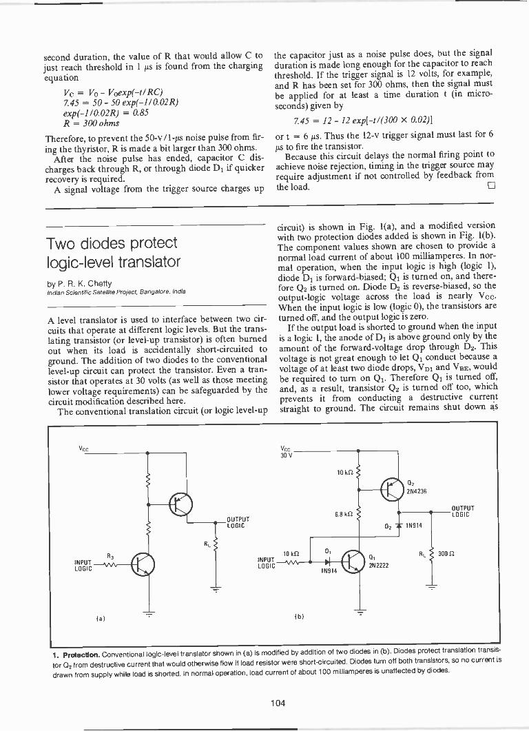
second duration, the value of R that would allow C tojust reach threshold in 1µs is found from the chargingequation
Vc = Vo - Voexp(-t/ RC)7.45 = 50 - 50 exp(-1/ 0.02R)exp(-1 /0.02R) = 0.85R = 300 ohms
Therefore, to prevent the 50 -v/1 -µs noise pulse from fir-ing the thyristor, R is made a bit larger than 300 ohms.
After the noise pulse has ended, capacitor C dis-charges back through R, or through diode D1 if quickerrecovery is required.
A signal voltage from the trigger source charges up
the capacitor just as a noise pulse does, but the signalduration is made long enough for the capacitor to reachthreshold. If the trigger signal is 12 volts, for example,and R has been set for 300 ohms, then the signal mustbe applied for at least a time duration t (in micro-seconds) given by
7.45 = 12 - 12 exp[-t/(300 x 0.02)]
or t = 6µs. Thus the 12-v trigger signal must last for 6to fire the transistor.Because this circuit delays the normal firing point to
achieve noise rejection, timing in the trigger source mayrequire adjustment if not controlled by feedback fromthe load.
Two diodes protectlogic -level translatorby P. R. K. ChettyIndian Scientific Satellite Project, Bangalore, India
A level translator is used to interface between two cir-cuits that operate at different logic levels. But the trans-lating transistor (or level -up transistor) is often burnedout when its load is accidentally short-circuited toground. The addition of two diodes to the conventionallevel -up circuit can protect the transistor. Even a tran-sistor that operates at 30 volts (as well as those meetinglower voltage requirements) can be safeguarded by thecircuit modification described here.
The conventional translation circuit (or logic level -up
circuit) is shown in Fig. 1(a), and a modified versionwith two protection diodes added is shown in Fig. 1(b).The component values shown are chosen to provide anormal load current of about 100 milliamperes. In nor-mal operation, when the input logic is high (logic 1),diode D1 is forward -biased; Qi is turned on, and there-fore Q2 is turned on. Diode D2 is reverse -biased, so theoutput -logic voltage across the load is nearly We.When the input logic is low (logic 0), the transistors areturned off, and the output logic is zero.
If the output load is shorted to ground when the inputis a logic 1, the anode of D1 is above ground only by theamount of the forward -voltage drop through D2. Thisvoltage is not great enough to let Q1 conduct because avoltage of at least two diode drops, VD1 and VBE, wouldbe required to turn on Q. Therefore Qi is turned off,and, as a result, transistor Q2 is turned off too, whichprevents it from conducting a destructive currentstraight to ground. The circuit remains shut down as
vcc
(a)
OUTPUTLOGIC
10 kftINPUTLOGIC
lb)
OUTPUTLOGIC
1. Protection. Conventional logic -level translator shown in (a) is modified by addition of two diodes in (b). Diodes protect translation transis-
tor 02 from destructive current that would otherwise flow if load resistor were short-circuited. Diodes turn off both transistors, so no current is
drawn from supply while load is shorted. In normal operation, load current of about 100 milliamperes is unaffected by diodes.
104

2. Waveforms. During normal operation of the logic -level translator,the output voltage and the current from the Vey supply go on and off
as the input logic goes high and iow. If output load is short-circuited,diodes turn off transistors so that no currents flow.
long as the load is short-circuited, and it returns to nor-mal operation when the short is removed.
Levels of input -logic voltage, output -logic voltage,and current from the high -voltage supply are shown inFig. 2 for both normal operation of the circuit and theshort -circuited -output condition. No current is drawnfrom the Vcc supply while the load is grounded.
INPUT LOGICVOLTAGE
5V
OUTPUT LOGIC30 V
VOLTAGE 0
SUPPLYCURRENT
100 mA
OUTPUT LOADSHORT-CIRCUITED
Power -supply add-onyields variable -ratio outputby Ying-Lau LeeCambridge, Mass.
A single -ended power supply can be converted into adouble -ended supply with the addition of an oper-ational amplifier, a transistor, and a few resistors. Thetwo output voltages need not be equal and in fact canbe made to have a ratio as big as 10:1 with the properchoice of resistor values.
The circuit is simple and works essentially as a paral-lel regulator. Potentiometer R1 is set to the desired ratioof VI /V2; the 741 operational amplifier then comparesthe potentiometer voltage with the voltage at the collec-tor of transistor Q and tries to minimize the differenceby biasing Q to produce that ratio. If V2 is too large, forexample, the op amp drives Q farther into conduction.The drop across Q (i.e., V2) then decreases.
The values of resistors R2 and R3 depend upon themaximum load allowed, input voltage, output voltageratio, and transistor current gain hFE. Approximate val-
ues for these resistors are calculated as follows:
R2 = 0.8 (Vi/ V2)RL2R3 = hFE VINRIAR2/ Vl(RL1 + R2)
With R2 and R3 fixed, Vi /V2 can be varied ±10% by ad-justment of R3.
If the outputs were balanced, no current would flowto ground. For unbalanced outputs, Q and R2 carry theground current. Transistor Q must be able to dissipate apower given by the following equation:
+R2)/RL1R2PD = V1VOL1
The SK3021 transistor that is suggested in theschematic can dissipate 35 watts, but a lower -power de-vice will be satisfactory in many cases. If Q drains toomuch current from the 741, a Darlington pair should beused to provide greater current gain.
Regulation of the output voltages is approximatelythat of the floating supply that is their source. The min-imum value of output voltage V2 is about 3 v (limitedby the 741). The 741 is used for the operational ampli-fier because it is internally compensated and has over-load protection.
Two for one. Double -ended supply provides positive and negative voltages from a single source. Output voltages can be equal, or in ratio asgreat as 10:1. Potentiometer allows adjustment of V1/V2 around a "ballpark" value determined by resistors in circuit.
105
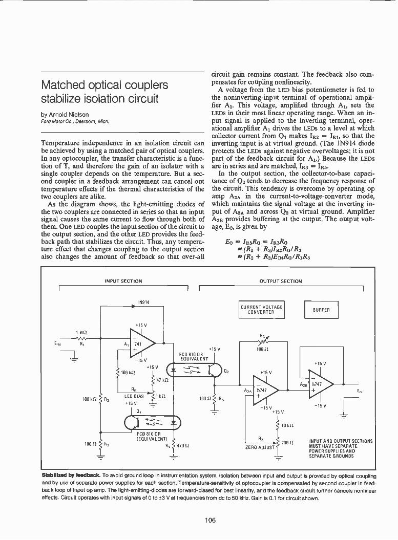
Matched optical couplersstabilize isolation circuitby Arnold NielsenFord Motor Co., Dearborn, Mich.
Temperature independence in an isolation circuit canbe achieved by using a matched pair of optical couplers.In any optocoupler, the transfer characteristic is a func-tion of T, and therefore the gain of an isolator with asingle coupler depends on the temperature. But a sec-ond coupler in a feedback arrangement can cancel outtemperature effects if the thermal characteristics of thetwo couplers are alike.
As the diagram shows, the light -emitting diodes ofthe two couplers are connected in series so that an inputsignal causes the same current to flow through both ofthem. One LED couples the input section of the circuit tothe output section, and the other LED provides the feed-back path that stabilizes the circuit. Thus, any tempera-ture effect that changes coupling to the output sectionalso changes the amount of feedback so that over-all
circuit gain remains constant. The feedback also com-pensates for coupling nonlinearity.
A voltage from the LED bias potentiometer is fed tothe noninverting-input terminal of operational ampli-fier Al. This voltage, amplified through A1, sets theLEDs in their most linear operating range. When an in-put signal is applied to the inverting terminal, oper-ational amplifier Al drives the LEDs to a level at whichcollector current from Qi makes 1R2 = hi, so that theinverting input is at virtual ground. (The 1N914 diodeprotects the LEDs against negative overvoltages; it is notpart of the feedback circuit for A1.) Because the LEDsare in series and are matched, IR3 = IRS
In the output section, the collector -to -base capaci-tance of Q2 tends to decrease the frequency response ofthe circuit. This tendency is overcome by operating opamp A2A in the current -to -voltage -converter mode,which maintains the signal voltage at the inverting in-put of A2A and across Q2 at virtual ground. AmplifierA2B provides buffering at the output. The output volt-age, E0, is given by
Eo = /RS& = /R3RGal (R2 + R3)IR2RGI R3N (R2 + R3)EINRO R1R3
1 MS2
EIN R1
INPUT SECTION
I
1N914
100 kS2
100
R2
Al
+15 V
741
-15 V
100 kS2
+15 V
47 kS2
RB
LED BIAS 11(2
+15 V
1
OUTPUT SECTION
+15 VFCD 810 OREQUIVALENT
FCD 810 OR(EQUIVALENT)
R4 470 S-2
CURRENT -VOLTAGECONVERTER
100 R
A2A
100 SZ
+15 V
'/:747
-15 V
BUFFER
A28
+15 V
Rz
ZERO ADJUST
10 kS2
200
+15 V
Y:747
-15 V
Eo
INPUT AND OUTPUT SECTIONSMUST HAVE SEPARATEPOWER SUPPLIES ANDSEPARATE GROUNDS
Stabilized by feedback. To avoid ground loop in instrumentation system, isolation between input and output is provided by optical couplingand by use of separate power supplies for each section. Temperature -sensitivity of optocoupler is compensated by second coupler in feed-back loop of input op amp. The light -emitting -diodes are forward -biased for best linearity, and the feedback circuit further cancels nonlineareffects. Circuit operates with input signals of 0 to ±3 Vat frequencies from dc to 50 kHz. Gain is 0.1 for circuit shown.
106
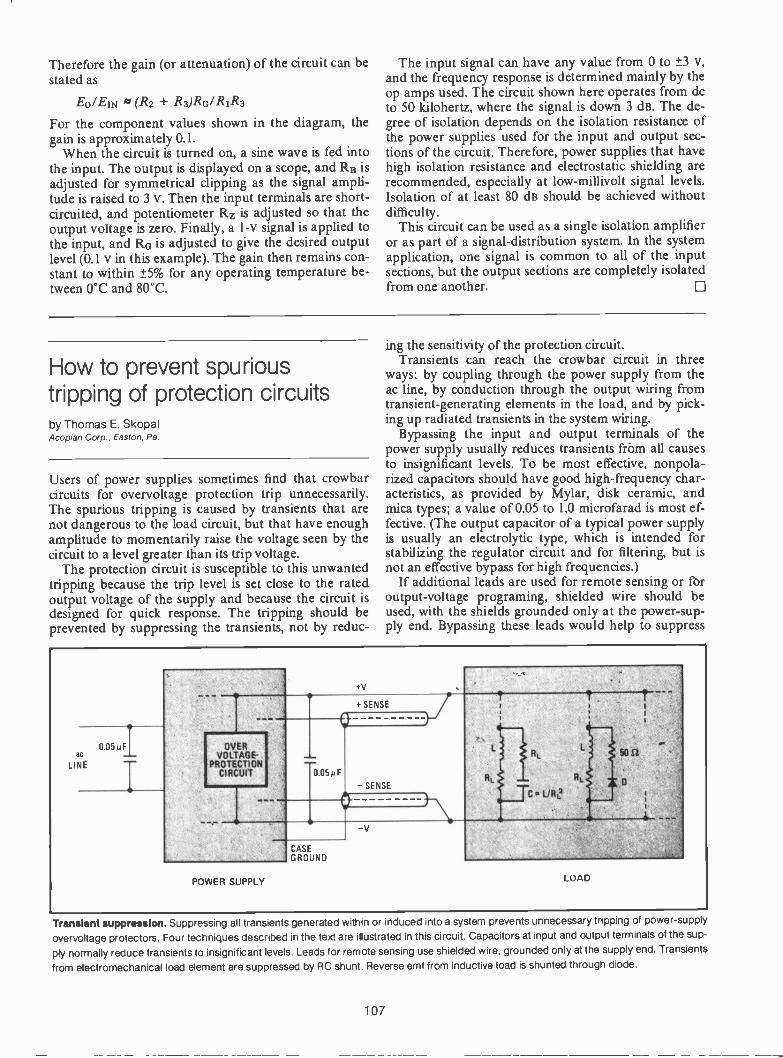
Therefore the gain (or attenuation) of the circuit can bestated as
Eo/EIN Ai (R2 + R3)RG/RIR3
For the component values shown in the diagram, thegain is approximately 0.1.
When the circuit is turned on, a sine wave is fed intothe input. The output is displayed on a scope, and RB isadjusted for symmetrical clipping as the signal ampli-tude is raised to 3 v. Then the input terminals are short-circuited, and potentiometer Rz is adjusted so that theoutput voltage is zero. Finally, a 1-v signal is applied tothe input, and RG is adjusted to give the desired outputlevel (0.1 v in this example). The gain then remains con-stant to within ±5% for any operating temperature be-tween 0°C and 80°C.
The input signal can have any value from 0 to ±3 v,and the frequency response is determined mainly by theop amps used. The circuit shown here operates from dcto 50 kilohertz, where the signal is down 3 dB. The de-gree of isolation depends on the isolation resistance ofthe power supplies used for the input and output sec-tions of the circuit. Therefore, power supplies that havehigh isolation resistance and electrostatic shielding arerecommended, especially at low -millivolt signal levels.Isolation of at least 80 dB should be achieved withoutdifficulty.
This circuit can be used as a single isolation amplifieror as part of a signal -distribution system. In the systemapplication, one signal is common to all of the inputsections, but the output sections are completely isolatedfrom one another.
How to prevent spurioustripping of protection circuitsby Thomas E. SkopalAcopian Corp., Easton, Pa.
Users of power supplies sometimes find that crowbarcircuits for overvoltage protection trip unnecessarily.The spurious tripping is caused by transients that are
amplitude to momentarily raise the voltage seen by thecircuit to a level greater than its trip voltage.
The protection circuit is susceptible to this unwantedtripping because the trip level is set close to the ratedoutput voltage of the supply and because the circuit isdesigned for quick response. The tripping should beprevented by suppressing the transients, not by reduc-
ing the sensitivity of the protection circuit.Transients can reach the crowbar circuit in three
ways: by coupling through the power supply from theac line, by conduction through the output wiring fromtransient -generating elements in the load, and by pick-ing up radiated transients in the system wiring.
Bypassing the input and output terminals of thepower supply usually reduces transients from all causesto insignificant levels. To be most effective, nonpola-rized capacitors should have good high -frequency char-acteristics, as provided by Mylar, disk ceramic, andmica types; a value of 0.05 to 1.0 microfarad is most ef-fective. (The output capacitor of a typical power supplyis usually an electrolytic type, which is intended forstabilizing the regulator circuit and for filtering, but isnot an effective bypass for high frequencies.)
If additional leads are used for remote sensing or foroutput -voltage programing, shielded wire should beused, with the shields grounded only at the power -sup-ply end. Bypassing these leads would help to suppress
0.05 p Fac
LINE
+v
OVERVOLTAGE -
PROTECTIONCIRCUIT
+SENSE
0.05 µ F
- SENSERi
C Ulte
50 52
CASEGROUND
tv
POWER SUPPLY LOAD
Transient suppression. Suppressing all transients generated within or induced into a system prevents unnecessary tripping of power -supplyovervoltage protectors. Four techniques described in the text are illustrated in this circuit. Capacitors at input and output terminals of the sup-
ply normally reduce transients to insignificant levels. Leads for remote sensing use shielded wire, grounded only at the supplyend. Transients
from electromechanical load element are suppressed by RC shunt. Reverse emf from inductive load is shunted through diode.
107

transients, but would also tend to slow the response ofthe supply, so shielded wire is used instead.
Crowbar operation is affected by electromechanicalcomponents in the load. Relays, counters, and solenoidstend to generate sizable transients that can damage asensitive circuit; therefore, such transients must be sup-pressed at their source. They are most effectively sup-pressed by an RC network across the inductance.(Resistance in series with the bypass capacitor is neces-sary to prevent the high current surge that would other-wise flow into C when the load is energized. This cur-rent would burn switch contacts and cause noise.) Theresistor value should equal the resistance of the load
component, RL, and the capacitor value should beequal to L/RL2, where L is the load inductance.
As an alternative, transients from an inductive com-ponent in a dc circuit may be suppressed simply by adiode connected across the component, back -biasedrelative to the supply voltage. The reverse voltage re-sulting from collapse of the magnetic field is shuntedthrough the diode, and its amplitude is limited to theforward drop of the diode. However, this shunt diodetends to slow turnoff The decay time -constant is givenby L/(RL + Itthode); if speed is critical, some suppres-sion can be sacrificed for speed by adding a resistor (50to 500 ohms) in series with the diode.
555 as switching regulatorsupplies negative voltageby S L BlackWestern Electric Co , Columbus, Ohio
Latest addition to the 555 Ic timer's seemingly endlessbag of tricks is its use to generate a negative dc biasingvoltage from a positive source. A current of well over 10milliamperes can be delivered, and a form of switchingregulation is employed to assure a constant output volt-age. All of this is done with little more than an npntransistor and the 555 integrated circuit.
The 555 is operated in the astable mode, with thepulse width and frequency controlled by resistors R1and R2 plus capacitor C1. These parameters can be se-lected for maximum regulation at the output voltagelevel desired. Terminal 3 of the lc is connected to a net-work consisting of C2, C3, and diodes D1 and D2. Seriescapacitor C2 causes the pulse train to lose its ground ref-erence, so that D1 and D2 can rectify the signal and ca-
pacitor C3 can filter it into a negative dc output voltage.The magnitude of this output voltage depends on theamplitude and repetition rate of the pulses coming fromthe IC.
To regulate the output voltage, the 2N2222 transistorvaries the control voltage of the 555, increasing or de-creasing the pulse repetition rate. Resistor R3 acts as acollector load for the transistor; the base is driven frompotentiometer R4, which compares the output voltage tothe supply voltage. If the output voltage becomes lessnegative, the control voltage goes closer to ground,causing the repetition rate of the 555 to increase so thatC3 recharges more frequently. If the output voltage be-comes more negative, the control voltage goes closer tothe positive supply voltage, so the repetition rate de-creases, and C3 is recharged less often.
The output voltage can be set to any level from 0 to-10 volts by means of potentiometer R4. With the com-ponents shown in the figure, this circuit supplies -10 vfrom a 12-v source. Regulation is less than 5% at a cur-rent of 10 mA and less than 0.05% at 0.2 mA.
+12 V
RI
4.7 kt2
R2
1 U1
Cl
0.01 NF
12V
VOLTAGEAT POINT A
Ra
250 kS2 0
VOLTAGEAT POINT B
OUTPUTLOAD
-12 V
0
OUTPUTVOLTAGE
-12 VPULSE RATE
DEPENDS ON LOAD 4-
Negative-voltage source. Pulses from free -running multivibrator ICare inverted and smoothed by C2, D2, and C3. Negative output volt-age across C3 is regulated by the transistor, which increases or de-creases multivibrator frequency to charge C3 as often.as necessary.With components shown, output is -10 V. Regulation is 0.05% at 0.2mA and 5% at 10 mA, providing good bias supply.
108

Logic gates and LEDindicate phase lockby R. P. LeckBell Laboratories, Crawford Hill, Holmdel, N.J.
Phase -locked loops are widely used for signal processingand digital applications such as fm demodulation, tone -decoding, and clock synchronization. If the error signalis accessible, signal acquisition and locking in the PLLcan be observed from decrease of error voltage to zero.For integrated -circuit PLLs without an error -signal ter-minal, however, acquisition and lock can be indicatedby two exclusive -OR gates and a light -emitting diode.The LED glows brightly when the input signal is first ap-plied, then dims as the loop signal pulls into synchro-nism, and it goes out when the loop locks.
If the locked signal from the loop were in phase withthe input to the loop, a single exclusive -OR gate wouldsuffice for the indicator. In fact, however, the locked sig-nal lags the input by 90°, so a second gate is needed to
introduce an extra quadrature shift on either the inputor output signal. As shown in the figure, the phase isshifted by applying frequencies f and 2f to an exclusive -OR gate. In the circuit shown here, the extra 90° isadded to the locking signal before it goes into the loop;this procedure is convenient when f is generated bycounting down from a master oscillator, because 2f isreadily available.
From the square waves at f and 2f, gate 1 developsthe 90° -shifted signal f that is the input to the loop -phase detector. Gate 2 functions as an auxiliary phasedetector, comparing the phase between the loop output,fp, and the non -phase -shifted input f. The output fromgate 2, fD, drives the light -emitting diode that indicatesacquisition and lock.
When the loop is locked and its natural frequency isclose to f, the inputs to the detector coincide. The result-ing pulse width of the signal present at its output is ei-ther tiny or nonexistent, so the LED is turned off. Whenthe loop is out of lock and its natural frequency is farfrom f, maximum output pulse width is obtained andthe LED is turned on at its maximum brightness. As theloop acquires lock, the output -pulse width decreases,decreasing the brightness of the LED.
2f
2f
'A SN7486
PHASE -SHIFTING IN GATE 1
to
fo
DETECTOR OUTPUT FROM GATE 2
UNLOCKED LOCKED
Loop monitor. Phase -locked loop has LED monitor that glows brightly when loop is unlocked, dims as loop nears sync, and is dark at lock.Output from loop lags input by 90°; therefore, to permit comparison of output with locking signal, signal is shifted 90° before entering loop.
ECL IC oscillatesfrom 10 to 50 MHzby William A. PalmControl Data Corp., Minneapolis, Minn.
One of the simplest of oscillators, the emitter -coupled -logic type outlined in Fig. 1, uses one third of the cir-cuitry of an MC10116 ECL integrated circuit. Besidesthe lc, the only elements required for the oscillator are
resistor R and capacitor C. The frequency of oscillationequals 1/3.4 RC.
Details of the oscillator are shown in Fig. 2. Transis-tor Qi is a constant -current source for the differentialamplifier made up of Q4 and Q5. The output signal,taken from emitter -follower Q2 at pin 2, is fed back toQ4 as the oscillator reference voltage at pin 4. Thus,pins 2 and 4 are always at the same voltage, and theyswitch between the ECL levels shown in the waveforms.
Operation of the circuit is indicated by the waveformsof voltage at pins 2 and 4, and at pin 5. The capacitorcharges and discharges through resistor R when pins 2and 4 go higher or lower than pin 5. When pins 2 and 4
109
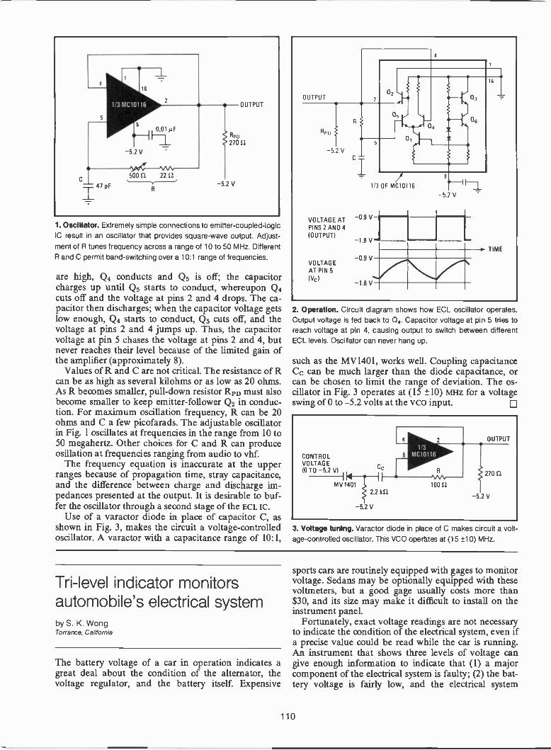
1. Oscillator. Extremely simple connections to emitter -coupled -logicIC result in an oscillator that provides square -wave output. Adjust-
ment of R tunes frequency across a range of 10 to 50 MHz. DifferentR and C permit band -switching over a 10:1 range of frequencies.
are high, Q4 conducts and Q5 is off; the capacitorcharges up until Q5 starts to conduct, whereupon Q4cuts off and the voltage at pins 2 and 4 drops. The ca-pacitor then discharges; when the capacitor voltage getslow enough, Q4 starts to conduct, Q5 cuts off, and thevoltage at pins 2 and 4 jumps up. Thus, the capacitorvoltage at pin 5 chases the voltage at pins 2 and 4, butnever reaches their level because of the limited gain ofthe amplifier (approximately 8).
Values of R and C are of Rcan be as high as several kilohms or as low as 20 ohms.As R becomes smaller, pull -down resistor RPD must alsobecome smaller to keep emitter -follower Q2 in conduc-tion. For maximum oscillation frequency, R can be 20ohms and C a few picofarads. The adjustable oscillatorin Fig. 1 oscillates at frequencies in the range from 10 to50 megahertz. Other choices for C and R can produceosillation at frequencies ranging from audio to vhf.
The frequency equation is inaccurate at the upperranges because of propagation time, stray capacitance,and the difference between charge and discharge im-pedances presented at the output. It is desirable to buf-fer the oscillator through a second stage of the ECL IC.
Use of a varactor diode in place of capacitor C, asshown in Fig. 3, makes the circuit a voltage -controlledoscillator. A varactor with a capacitance range of 10:1,
OUTPUT
Rv0
-5.2 V
1/3 OF MC10116
VOLTAGE ATPINS 2 AND 4(OUTPUT)
VOLTAGEAT PIN 51\0
-5.2 V
TIME
2. Operation. Circuit diagram shows how ECL oscillator operates.Output voltage is fed back to 04. Capacitor voltage at pin 5 tries toreach voltage at pin 4, causing output to switch between differentECL levels. Oscillator can never hang up.
such as the MV1401, works well. Coupling capacitanceCc can be much larger than the diode capacitance, orcan be chosen to limit the range of deviation. The os-cillator in Fig. 3 operates at (15 -±10) MHz for a voltageswing of 0 to -5.2 volts at the vco input. 0
3. Voltage tuning. Varactor diode in place of C makes circuit a volt-age -controlled oscillator. This VCO opettes at (15 ±10) MHz.
Tri-level indicator monitorsautomobile's electrical systemby S. K. WongTorrance, California
The battery voltage of a car in operation indicates agreat deal about the condition of the alternator, thevoltage regulator, and the battery itself. Expensive
sports cars are routinely equipped with gages to monitorvoltage. Sedans may be optionally equipped with thesevoltmeters, but a good gage usually costs more than$30, and its size may make it difficult to install on theinstrument panel.
Fortunately, exact voltage readings are not necessaryto indicate the condition of the electrical system, even ifa precise value could be read while the car is running.An instrument that shows three levels of voltage cangive enough information to indicate that (1) a majorcomponent of the electrical system is faulty; (2) the bat-tery voltage is fairly low, and the electrical system
110

should be checked; or (3) the battery voltage is ade-quate for efficient functioning of the system.
A solid-state tri-level voltage indicator that uses light -emitting diodes to show three voltage ranges can bebuilt for $5 to $10, depending on the quality of the partsused, and it is a bargain for the purpose it serves. Thecircuit shown in the diagram uses, in addition to thethree LEDs of different colors, three npn switching tran-sistors, two zener diodes, one blocking diode, and ahandful of 0.5 -watt resistors. The red and yellow combi-nation indicates a battery voltage of less than 11.7 v,yellow shows 11.7 to 12.7 v, and the green light showsthat the battery voltage is 12.7 v or more.
If the battery voltage is below 11.7 v, all of the tran-sistors are turned off. Diode D4 blocks the current paththrough green LED D3, the base and collector of Qz, D2,and D1, so that current flows only through R2, D2, andD1. The red and yellow LEDs light up to indicate thatthe battery, voltage regulator, alternator, or any combi-nation of the three, is bad.
If the voltage is between 11.7 and 12.7 v, transistorsQ2 and Q3 are still turned off, but zener ZD1 conductsand lets Qi turn on to shunt out the red LED. Thus onlythe yellow LED lights up, warning the driver of a fairlylow battery voltage. Unless this low -voltage situationimproves after a few miles of driving, the electrical sys-tem of the car should be inspected for faults or highcontact resistances.
If the battery voltage quickly reaches 12.7 v or moreafter the car is started, Q3 also turns on. Currentthrough Q3 lights the green LED and also turns on Q2 toshunt out the yellow LED. The resulting green light as-sures the driver of a functioning electrical power systemin his car.
The user may choose zener diodes with somewhat dif-ferent breakdown voltages if he wants to shift the threeindication levels to fit his own requirements. El
+V8 (FROM IGNITION SWITCH)
100 1-2
ZDi(11 V)
1N4741A
R7
10 ks-2
-V8
2N2219A
R2
390 11
1N4001
YELLOWHP5082-4550 02
RED
HP5082-4650
2N2219A
vw GREENHP5082-4950
R4
390 S2
R5
47 S2
2N2219A
BATTERY VOLTAGE LEDs LIGHTED
V5 < 11.7 V RED AND YELLOW
11.7 V < VB < 12.7 V YELLOW
V5 .->, 12.7 V GREEN
R6
100 ft
ZG2x% (12 V)
1N4742A
R5
10 kfl
Battery -voltage Indicator. Colored LEDs indicate three ranges of battery voltage in car. A weak battery turns on red and yellow, a strongerbattery breaks down 11-V zener to light only yellow, and a strong battery turns on green as both zeners conduct. Resistors R7 and R8 provide
high -temperature stability. This unit can warn of need for corrective maintenance of car's electrical system.
111

Monostable's pulse widthis programableby C.F. ReevesDel Mar, Calif.
Variable -width pulses are required in many systems,and the widespread use of microprocessors as controlelements makes numerical control of the pulse widthsincreasingly important. A numerically controlled one-shot multivibrator can be built that is particularly usefulwhen the pulse -width range required is impractical orunattainable with conventional RC -time -constant one -shots.
For each input trigger pulse, the circuit produces anoutput pulse whose width is determined by an inputbinary number. The number may be taken from binaryor binary -coded -decimal (BCD) sources such as shift
registers, counters, bistable latches, thumbwheelswitches, or the like.
Functionally, the circuit is identical to the conven-tional one-shot in that it has one stable state and onetemporary or quasistable state. The fundamental differ-ence lies in the timing element that determines howlong the circuit can remain in the quasistable state. Inthe conventional one-shot, this monostable period is setby the time constant of a resistor -capacitor network.The circuit shown here sets the monostable period bycounting a preselected number of periods of a clockoscillator.
The range is thus limited only by the number ofcounter stages used. In Fig. 1 gates 2A and 2B form aclock oscillator that is gated on by a high logic level atpin 1. Resistors R1 and R2 and capacitor C1 set the fre-quency at 10 megahertz. Gate 2C is an inverting bufferfor the output pulses from the clock.
The input trigger pulse loads the counter chain (com-ponents 3 through M) with the number supplied by thebinary data source. Simultaneously the trigger sets an
coOSCILLATOR
10012
R2 220 E2
OUTPUTPULSEVouT
FLIP-FLOP
10 D
1;80 pF
BINARY DATA SOURCE
(COUNTERS, LATCHES, SHIFT REGISTERS,
THUMBWHEEL SWITCHES, ...
LS8 MSB
0
CURRENT -LIMITED5-V SOURCE
13
4-5V
14
COUNTER
11=
zo
2 13
AINPUT TRIGGER
PULSE
ClCURRENT -LIMITED5-V SOURCE
10 13
ACLEAR
0 SN7400
0 SN74860-0 SN74192 (BCD)
OR SN74193 (BINARY)
1. By the numbers.. Binary number set into counter from data source determines duration of output pulse from this monostable circuit wheninput trigger pulse is applied. Output voltage VouT is high while counter counts the given number of cycles from the oscillator, as shown inFig. 2. Typical applications for this circuit include variable -time -delay generation and pulse -code modulation.
112

INPUTTRIGGER
VOLTAGEAT POINT
X
VOLTAGEAT POINT
V
VOLTAGEAT POINT
z
CLEAR
VoUT
5 V r0
5 v r
D
5 V r
0 L
5 V r
0 L
5v rOIL
5 r
NTH COUNT
U
RETRIGGER PULSE
I ME -1111 11-
OUTPUT WITHOUT RETFOGGEROUTPUT WITHOUT CLEAR
2. Count. Waveforms for one-shot multivibrator in Fig. 1 illustrate
operation. Input trigger makes VouT high and starts oscillator.
Counter counts N cycles of oscillation (where N is decimal value ofbinary number set on counter by control source), then makes WWI'low and stops oscillator. A trigger pulse applied during operationprolongs output pulse through countdown of newly loaded number.Output can be cut off at any time by grounding the clear terminal.
R/S flip-flop (1A and 1B), the output of which gates onthe 10 -MHz clock oscillator. The clock pulses cause thecounter chain to count down to zero, whereupon theborrow pulse is generated at point Z. The borrow pulseresets the R/S flip-flop, disabling the clock oscillatorand terminating the output pulse.
The width of the output pulse is determined by thebinary input data and the clock frequency according tothe following relationship:
PW = (N+ 1)/f,.
where N is the decimal value of the binary input num-ber, and f1. is the clock frequency. The numerator is(N+ 1) instead of N because the counter generates theborrow pulse when leaving the zero state rather thanwhen entering it. The output pulse -width range is deter-mined by the number of 4 -bit counter stages, K, and isexpressed as 1:10K for BCD input data and 1:16K forbinary input data. As the waveforms of Fig. 2 show, theone-shot is retriggerable. When an input trigger pulseoccurs while the counter chain is counting down from aprevious trigger, the chain simply reloads with the valueof the binary data source and begins a new countdown.The result is a single elongated pulse. An additional cir-cuit feature is that the output pulse may be terminatedat any time by applying the logic zero to the "clear" in-put terminal. 0
Current and power limiterprotects switching transistorby R.M. StittBurr -Brown Research Corp., Tucson. Ariz.
Although a switching transistor dissipates little power innormal operation, it must be protected from destructivecurrent and power overloads. Current -limiting alone isnot sufficient protection; power -limiting is also neces-sary. But fortunately, a few components can be addedto conventional current -limiting circuitry to providepower -limiting. A voltage rise across a transistor issensed and used to cut down the drive current.
To understand why current -limiting alone fails toprovide adequate protection, consider a switching tran-sistor controlling a 100 -ohm load connected to a 100 -volt supply. The power dissipated in the load might beabout 100 watts, but the maximum power dissipated inthe transistor is merely the load current times the tran-sistor's saturation voltage (if switching losses are ne-glected). The load current is about 1 ampere, so thetransistor dissipates less than 1 w. A designer might usea 3-w device and provide a current -limiting level of 1.5amperes.
Suppose, however, that the load is short-circuited so
*CATCHDIODE1N4003
_J (FORINDUCTIVELOAD)
Two-way protection. Switching transistor 01 is protected againstexcess current and/or excess power dissipation. If load current ap-proaches limit, IR2 drop turns on transistor 02 to shunt base drivefrom 01. A voltage rise across 01 acts through R3 to turn on 02 andturn off 01. Capacitor C provides delay that allows 02 to saturatewith each new cycle, and lets power -limiter ignore transient highcurrents. Diodes D1 and D2 reset power -limiter when input is low.
113
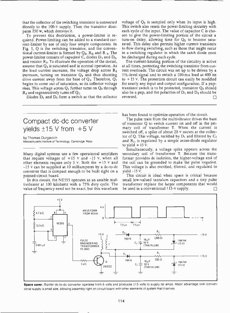
that the collector of the switching transistor is connecteddirectly to the 100-v supply. Then the transistor dissi-pates 150 w, which destroys it.
To prevent this destruction, a power -limiter is re-quired. Power -limiting can be added to a standard cur-rent -limiter by use of only four simple components. InFig. 1, Q is the switching transistor, and the conven-tional current -limiter is formed by Q2, R2, and R 4. Thepower -limiter consists of capacitor C, diodes D1 and D2,and resistor R3. To illustrate the operation of the circuit,assume that Qi is saturated and in normal operation. Asthe load current increases, the voltage drop across R2
increases, turning on transistor Q2 and thus shuntingdrive current away from the base of Qi. Therefore, Qibegins to come out of saturation, so its collector voltagerises. This voltage across Q1 further turns on Q2 throughR3 and regeneratively turns off Q.
Diodes D1 and D2 form a switch so that the collector
voltage of Qi is sampled only when its input is high.This switch also resets the power -limiting circuitry witheach cycle of the input. The value of capacitor C is cho-sen to give the power -limiting portion of the circuit aturn -on delay, allowing time for Q2 to become satu-rated. This delay also permits higher current transientsto flow during switching, such as those that might occurin a switching regulator in which the catch diode mustbe discharged during each cycle.
The current -limiting portion of the circuitry is activeat all times, protecting the switching transistor from cur-rent overloads. The circuit was set up to be driven by aTn.-level signal and to switch a 100-mA load at 400 Hzto + 15 v. The protection circuit can easily be modifiedfor nearly any input and output configuration. If a pnp-transistor switch is to be protected, transistor Q2 shouldalso be a pnp, and the polarities of D1 and D2 should bereversed.
Compact dc -dc converteryields ±15 V from +5 Vby Thomas DurgavichMassachusetts Institute of Technology, Cambridge, Mass.
Many digital systems use a few operational amplifiersthat require voltages of +15 v and -15 v, when allother elements require only 5 v. Both the +15 v and-15 v can be supplied at 10 milliamperes by a dc -to -dcconverter that is compact enough to be built right on aprinted -circuit board.
In this circuit, the NE555 operates as an astable mul-tivibrator at 100 kilohertz with a 75% duty cycle. Thevalue of frequency need not be exact, but this waveform
has been found to optimize operation of the circuit.The pulse train from the multivibrator drives the base
of transistor Q to switch current on and off in the pri-mary coil of transformer T. When the current isswitched off, a spike of about 20 v occurs at the collec-tor of Q. This voltage, rectified by D1 and filtered by C1and R1, is regulated by a simple zener-diode regulatorto yield + 15 v.
Simultaneously, a voltage spike appears across thesecondary coil of transformer T. Because the trans-former provides dc isolation, the higher -voltage end ofthe coil can be grounded to make the pulse negative.This voltage is also rectified, filtered, and regulated toyield -15 v.
This circuit is ideal when space is critical becausesmall low -valued tantalum capacitors and a tiny pulsetransformer replace the larger components that wouldbe used in a conventional ± 15-v supply.
+5 V
4 7 kS2
3.3 kS2
1-0.001µF
4VWAVEFORMFROM NE555
NE555 +7.5ms 2.5ps
+5
PULSE
p2
VR2
15V
1N914 10µF 1200521N4744
ENGINEERING C2 - 50 V (15 V)TRANSFORMER I(TANTALUM)
PE 3843
El, Ri
+15 V
a 1N914 10µF330 52
1N47441 I<S2
2N2222 C1-150V(TANTALUM)(15 V/
Space saver. Bipolar dc -to -dc converter operates from 5 volts and produces ±15 volts to supply op amps. Major advantage over conven-tional supply is small size, allowing assembly right on circuit board with other elements of system that it serves.
114
Microphone preamp getspower through signal cableby Don JonesHarris Semiconductor, Melbourne, Fla,
When a high -impedance microphone is at the end ofmore than 20 or 30 feet of cable, a preamplifier poweredby batteries is often placed at the microphone to pre-vent high -frequency loss and to enhance the signal-to-noise ratio. But a preamp can be made much more com-pact if instead of using batteries it is powered remotelyover the shielded or twisted -pair audio cable.
The hookup shown here is an unconventional appli-cation of an operational amplifier, but the performancewill please any broadcaster or audio enthusiast. Per-formance is definitely high fidelity. Frequency responseis better than ±1 decibel from 20 hertz to 20 kilohertz,and equivalent input noise is about 3 microvolts rmsover this band.
The diagram shows the circuit arrangement. In the
quiescent state, the output terminal (pin 6) of oper-ational amplifier Ai is biased by R1, R2, and R,3 toabout half the power supply voltage, with negativefeedback through R4. However, the audio -output signalis not taken from pin 6; instead, the audio output comesfrom pin 7, the V+ terminal of the op amp. This outputsignal is inverted with respect to the normal amplifieroutput, so even though the audio -input signal from themicrophone is fed into the inverting op -amp input ter-minal, the amplifier is actually noninverting. The gain(about 100) is determined by the ratio of R1 and R2,which form the feedback network from the V+ (audio -output) pin. The HA -911 op amp is used because itsnoise level (8 nV/Hz112, 0.35 pA/Hz172) and gain -band-width product (8 wiz) are many times better than thoseof general-purpose op amps.
In the power module, op amp A2 supplies about 12 vdc at 7 milliamperes through a 600 -ohm termination tothe cable; the dc power for the module can probably beobtained from the main amplifier. Instead of using thepower module, the power for the preamp could be sup-plied to the cable through a passive choke in series witha dc supply, but 150 henrys would be required to obtainthe same noise isolation from the dc line.
DYNAMIC MICROPHONE(HIGH -IMPEDANCE)
PREAMPLIFIER
MICROPHONE CABLE
POWER MODULE Ai,A2 HARRIS SEMICONDUCTOR HA 911
HIGH-LEVEL INPUT
MAIN AMPLIFIER
Two-way cable. Microphone cable carries power up to preamplifier and carries amplified signal down to main amp, tier. Preamp, mounted athigh -impedance microphone before long cable to preserve fidelity and suppress noise, is light and compact because its power is suppliedthrough the cable, eliminating batteries. Although op amps are used in unconventional arrangements, performance is excellent.
115

Converter changes 7 -segmentoutput to decimal or BCDby Prentice L. OrswellNational Oceanic and Atmospheric Administration, Boulder, Cob.
Calculator chips and other LSI circuits with outputscoded to drive seven -segment displays can have morevaried applications if the seven -segment outputs areconverted to decimal or binary-coded decimal. The con-verter described here accepts seven -segment mos sig-nals directly at voltages up to + 15 volts and providesdecimal and/or BCD outputs with blanking. It uses onlyfour packages, at a component cost of less than $5. (Fora seven -segment -to -decimal converter that used discretetransistors, gates, and an expensive demultiplexer, seeElectronics, August 8, 1974, p. 105.)
Only six of the segment outputs are required for thiscircuit. Four of them-b, e, f, and g-are applied to theinput terminals of an MC14028 IC; a and c are applied
to an MC14555, along with two signals from theMC14028. These two packages have a combined totalof 10 output terminals, one of which goes high to repre-sent a numeral (0 through 9) when the complements ofthe numeral's seven -segment voltages are applied at theinput; most LSI circuits provide complementary outputs.The 10 terminals are the decimal outputs. (Another out-put, corresponding to either 1 or 7, is discussed below.)
If BCD outputs are desired, the decimal outputs areconnected to the input terminals of a CD4071B and aCD4075B. These units provide a total of four outputterminals, which go high to represent the four BCD bits.
In the seven -segment -to -decimal portion of the cir-cuit, the MC14028 (which is a BCD -to -decimal decoder)uniquely determines six of the decimal outputs. Thecomplements of b, e, f, and g segment voltages for both1 and 7 decode to output Q7, and digits 4 and 9 bothdecode to Ql. To separate these in the MC14555 (whichis a dual binary -to- 1 -of -4 decoder), the complement of ais used as an additional input. Full blanking is assuredby applying the complement of c at the enable inputs.
Conversion to BCD from the decimal code could beaccomplished in several ways. An ideal one -package so -
SEGMENT
INPUTS
a
7 SEGMENT TO DECIMAL
e -T
fi
B
AE
QO
Q1
Q2Q3
-A
B
CD
0001Q2Q3Q4Q5
06Q7
Q8Q9
E
B
QO
01
Q2
Q3
MC 14555
111. 11 OR 7)
DECIMAL TO BCD
9 90 4 80
7
1 7060
w 85
2 4o0
11. 3
0
MC14028
CD4071 BCD4075B
302 0
11 OR 7)6
5
Converter. Complements of seven -segment voltages, fed into inputsof this circuit, produce high level on one of the decimal -output linesand (if the conversion is carried over to the BCD) on one or more ofthe BCD output lines. Thus for segment voltages that could display aseven -segment 5, inputs for the b and e segments are high, produc-ing a voltage on decimal output line marked 5; and if BCD -to -decimalstage is connected, lines marked 20 and 22 go high.
a
f/9e/ /c
d
20
7-SEG.DIGIT
SEGMENTaC a I3 g- T e
MC14028OUTPUT
SELECTED
0 000 0100 041 101 0111 Q7
2 010 0010 023 000 0011 Q34 101 0001 Q1
5 000 1001 Q96 000 1000 0.8
7 001 0111 Q7
8 000 0000 QO
9 000 0001 Q1
BLANK 111 1111 ALL LOW
116
lution would be a 10 -bit priority encoder, but this circuitis not available in c-mos, so at least two packages arerequired to implement the encoder. An 8 -bit priorityencoder and some gating would work. A more economi-
cal approach, using OR gates, is shown in the diagram.Note that one gate is saved for other uses by utilizingthe 1 -or -7 output. All of the BCD outputs go low withblanking. El
Capacitive transducer sensestension in muscle fibersby Robert M. WiseMedical College of Virginia, Richmond, Va.
Tension in muscle fibers can be measured by thesame capacitive transducers that measure displacementand pressure. The ubiquitous NE555 timer and anNE560B phase -locked loop combine with a speciallymade capacitor to produce an analog output wheneverthere's a change in capacitance. Tuned circuits are notrequired, and both size and stability of the timer permitdesign versatility.
The heart of the circuit is the timer. When pins 2 and6 are connected, the timer triggers itself and runs free asa multivibrator. The transducer charges through R1 andR2 and discharges through R2. The frequency is preciseand independent of supply voltage. Charge time is:
= 0.693 (Ri + R2) CT
Discharge time is:
t2 = 0.693 (R2) CT
Frequency of oscillation is then:
1.44f = 1/T =(R1 + 2R2) CT
Any frequency between 0.1 hertz and 100 kilohertz canbe selected; the component values shown in the figureare for a frequency of about 100 kHz.
The input signal to the 560B is phase -compared to aninternal voltage -controlled oscillator. Error signal at theoutput of the comparator is filtered, amplified, and fedback to the vco. Input frequency to the phase -lockedloop through pin 12 must be attenuated to facilitateproper lock and capture of the transducer signal by thevco. The voltage should be between 20 and 50 milli-volts peak to peak.
The frequency of the vCO, which should be adjustedto coincide with the zero -position frequency of thetransducer, is determined principally by the capacitorCv connected between pins 2 and 3 of the NE560B:
fvco = 300/Cvwhere Cv is expressed in microfarads. Fine adjustmentof fvco can be made by a regulating current injectedinto pin 6 through a 4.7-kilohm resistor and controlledby the setting of the 5-kilohm potentiometer. The zero -position frequency of the transducer is measured at pin12 of the phase -locked loop, and the vco frequency ismeasured from pin 5 through the 2N3393 emitter-fol-
R
1MS-2
R210162
+5V +15V
4
555 3
2
TRANSDUCER
CT
5-20p F
100 k q
6-1 1 162
152
VE_C 5608 6
0.003pF 5
10kS2-13 10
2N3393
5 ksi-ow
0.05pF1-1-CF
4.7 k
0.1pF 0.01p F
I
lk 12
vcoOUTPUT
OUTPUT
15ka
Frequency modulation. Capacitive transducer modulates frequencyof 555 multivibrator. Frequency is detected in 5608 phase -lockedloop that produces dc output voltage. Arrangement is stable andcompact, has fast response, and does not require any tuned circuits.
lower transistor to avoid pulling the vcO.A filter capacitor CF between pins 14 and 15 sets the
desired bandwidth of demodulated information. Theapproximate value of CF in microfarads can be foundfrom the formula
CF = 13/B
where B is the bandwidth in Hz. The 0.05-µF valueshown gives a clean output swing of 100 millivolts.
The de -emphasis network uses an external capaci-tance of 0.01 ILF in conjunction with an 8-kilohm inter-nal resistance at pin 10 to produce a 75 -microsecondtime constant for the demodulated output at pin 9. The100 my output swing rides on a 12-v offset voltage. 0
117
Digital word setsgain of amplifierby Craig J. HartleyBaylor College of Medicine, Houston, Texas
Digital control of gain or attenuation is often desirablein programable systems or when the gains of many cir-cuits have to be varied simultaneously. In the circuitshown, the gain or attenuation of an analog signal iscontrolled by means of a binary input. The circuit,which is similar to a multiplying digital -to -analog con-verter, uses a single 741 operational amplifier for gainor attenuation, plus two transistors for each control bit.
The circuit has two parts. The first is a noninvertingoperational amplifier; the second is a set of resistorsthat can be connected in parallel to produce variousvalues for an equivalent single resistor Rc betweenswitch S and ground.
The value of Rc is determined by the digital inputs.When the input labeled 1 is low, transistors Qi and Q2are saturated, so that the 100-kilohm resistor R is con-nected from switch S to ground. When input 1 is high,Qi and Q2 are off, so the bottom of R is open -circuited.
Similarly, if inputs 2, 4, and 8 are low, they connectR/2, R/4, and R/8 to ground. Therefore the control in-
puts can be considered as a binary number with nega-tive logic (high voltage = 0, low voltage = 1) so thatthe total resistance connecting the switch to ground is
Rc = R/Nwhere N is the value of the binary input number. Forexample, if N equals 5, the binary number is 0101,which means that inputs 1 and 4 are low; therefore Rand R/4 are connected in parallel to provide a resist-ance of R/5 from S to ground.
When switch S is in position A, the gain of the opamp is
GA = Eo/Ei = 1 + RF/Rc = 1+ NRF/R
The values of RF and R are equal, so
GA = / N = 1, 2, 3, 4, . . .
For a 4 -bit control word, the maximum GA value is 16.When the switch is in position B, the op amp is con-
nected as a voltage follower fed by a voltage divider, sothe gain is
GB = Rc/ + Rc) = (RI (R, + R/N)
Because Ri is equal to R,
GB = 1/ (N +1) = 1,1/2, 1/2, ...
Thus the circuit can amplify (switch position A) or at-tenuate (switch position B).
The circuit as shown will handle analog input levels
Programabie gain or attenuation. The operational -amplifier circuit has a gain of GA = N + 1 or GB = 1 /(N + 1), depending on whetherswitch S is set to position A or position B. The number N is the value of the negative -logic binary number applied to the digital inputs. If pro-gramable sign -reversal is required, a digitally controlled inverter [Electronics, March 6, p. 85] can be used in tandem with the amplifier.
118

of ±7 volts, and the digital inputs will accept rn., logic is about 0.02 v maximum in the B mode and 0.25 vlevels. The bias resistors and supply voltage can be var- maximum in the A mode and is a function of gain. Ad-ied as needed for use with other logic forms. The offset ditional digits can be added for finer control. 0
Bootstrap circuit generateshigh -voltage pulse trainby Lawrence H. BannisterCenter for Space Research, MIT, Cambridge, Mass.
A circuit can easily be built to generate a high -voltagepulse train from a low -voltage power supply. Such a cir-cuit is used in a recently developed spacecraft instru-ment to generate a 400 -hertz square wave with an am-plitude of 4 kilovolts from 20 identical 200 -volt stagesconnected in series. A high -voltage supply is not neededbecause each stage includes a capacitor that functionsas a floating power supply for the next stage. These ca-pacitors are charged in parallel and then connected inseries so that the pulse generator does its own dc -to -dcconversion.
The schematic of Fig. 1 is drawn to emphasize themodularity of the circuit. To simplify the explanation, itis assumed that all transistors and diodes are perfectswitches, having infinite impedance when turned offand zero voltage -drop when turned on.
Suppose, first, that transistors Q1-1, Q1-2, Ql-Nare all turned off. Then diodes D1-1, D1-2, . . . Di_N areforward -biased and transistors Q2-1, Q2-2, Q2 -N are
driven to saturation. Capacitor C1_1 charges through thepath D3-1, C1-1, D2-1, and Q2_1. Concurrently, C1-2charges through the path 133_2, C1-2, D2_2, and Q2_2. So,in this circuit condition, all of the capacitors charge inparallel, and the potential difference across each capaci-tor is equal to the supply line voltage of 200 volts:
= V1-2 = = V = +200 vVow. = V2 -N = V2-2 = V2-1 = 0
If, now, Qi-i is turned on, diode D1_1 no longer con-ducts, so Q2-1 turns off. Current through resistor R3-1then causes Q3..1 to turn on, and the emitter potential ofQ3-1 approaches its collector potential so that V2_1 = V= +200 v. And, because C1_1 was previously chargedto the supply voltage, V1_1 = V2_1 + V = 2V = +400v.
Now, regardless of the state of Q1-2, when V2_1 be-comes positive, D1-2 becomes reverse -biased, and there-fore Q2..2 turns off. Current through R3-2 then causesQ3-2 to turn on, and the emitter potential of this transis-tor approaches its collector potential so that:
V2..2 = V1..1 = 2V = + 400 V= V2-2 + V = 3V = +600 v
As illustrated by Fig. 2, this sequence continues alongthe series of stages, each stage increasing the positivelevel of the pulse by V volts. The final output voltage isNV volts, where N is the number of stages and V is the
111- : 2N222202- : 2N5058 (S)(13- : 2N5058 IS)
RI_ : 33R2- : 33 knR3- : 1 MS -2
DI- : 1N5623 C,- : 0.1µFD2- : 1N914D3_ : 1N5623
VouT
4kvi_n n0
1. Kilovolt generator. Square wave of 4 kV at 400 Hz is produced by circuit with 20 low -voltage stages. Each stage includes a capacitor (C1)
that acts as a floating power supply for the next stage. The capacitors are charged in parallel and then connected in series. If lower outputvoltage is desired, input can be applied to 01.2 or 01_3 or . . . instead of Q. (Actual circuit also includes elements shown in Fig. 3.)
119
2. Timing. The stages start switcning sequentially, as diodes D1_1, D1-2, . . . successively become back -biased, but after all stages areswitched, they change voltage levels concurrently. Therefore the rise time is essentially that of a single stage. Similarly, the fall time is essen-tially independent of the number of stages. The output amplitude is the product of the power -supply voltage and the number of stages.
supply voltage. Because the stages switch concurrently,the total pulse rise time is only slightly longer than therise time of one stage.
Smaller -amplitude pulses can be generated byswitching only the last few stages to the "high" state.For example, if Qi_i remains off, but Q1-2 is turned on,the first stage will remain in the "low" state with V1-1 =V = + 200 v but all subsequent stages will switch to the"high" state so that Vow = (N - 1)V. If only Qi_m isturned on, the preceding stages will remain in the "low"state and the output pulse amplitude will just be Vvolts. Generally, then, the output -pulse amplitude canbe selected in increments of V up to a maximum of NV.
The positive -going edge of the pulse generated by thecircuit of Fig. 1 is quite slow because, in each stage,when Q2 is turned off, the potential at the base of Q3 in-creases exponentially toward a limiting value. Further,the output impedance of the circuit is quite large be-cause the current in R3 approaches zero in the "high"state and Q3 never really saturates.
The circuit modification shown in Fig. 3 preventsthese problems by the use of positive feedback in andbetween the stages. R3 is connected to provide positivefeedback within the stage; when Q2 is turned off and Q3starts to conduct, the potential at the top end of R3 re-mains V volts above the potential at the emitter of Q3.Thus, the potential difference across R3 is sensibly con-stant, and Q3 is driven by a constant current supply sothat its base potential increases linearly until the base -collector junction is forward -biased. Q3 then behaveslike an inverted switch transistor with a very low offsetvoltage that is just the difference between the voltagedrops of the base -emitter and base -collector diodes.
R4 and C2 provide positive feedback from one stageto the immediately preceding stage to speed the switch-ing action. For example, when the stages switch to the"high" state, V2 -L increases toward LV while V2_m in-creases toward MV. The difference between these volt-ages, MV - LV = (L+ 1)V - LV = V, causes a tran-
3. Feedback. To achieve 400 -Hz operation, the circuit in Fig. 1 is
modified as shown here. Ras provide positive feedback within eachstage, and R4s and Cgs provide positive feedback from each stage tothe preceding stages. Without the feedback, rise time is about 1 ms;with feedback, rise and fall times are both less than 0.1 ms.
sient current through R44.4 that drives the base of Q3-1,positive more rapidly.
With these feedback connections, the operating cir-cuit produces a 400 -Hz square wave with rise and falltimes of about 100 microseconds that are essentially in-dependent of the number of stages switched. The num-ber of stages switched changes only the amplitude ofthe square wave; this amplitude can be selected in in-crements of 200 v, up to a maximum of 4,000 v for a 20 -stage circuit. The only high -voltage components are thediodes labelled D1 in Fig. 1. In the spacecraft instru-ment, series strings of diodes are used as D1 to providethe necessary isolation for the higher -voltage stages ofthe pulse generator.
120

D -a converter formsprogramable gain controlby Jim EdringtonThe Applied Research Laboratories, University of Texas, Austin, Texas
A monolithic multiplying digital -to -analog convertercan be used with an operational amplifier to produce asimple digitally controlled amplifier. Logic voltages ap-plied at the 10 input terminals of a converter such as theAnalog Devices AD7520 control the gain. These volt-ages can provide 210 discrete levels of amplification foran analog signal applied to the operational amplifier.The integrated circuit can handle analog signals up to±10 volts, and the digital input levels are compatiblewith transistor -transistor logic and complementary-Mos.
A BCD -to -decimal decoder drives the d -a converter inthe circuit of Fig. 1, giving gains as high as 60 decibelsin 10 6 -dB steps. The circuit requires only a few compo-nents because the multiplying converter Ic contains thec-mos switches and precision -resistor ladder networkthat set the gain of the amplifier.
The 741 op amp is connected as a conventional in-verting amplifier, with an input resistor and a feedbackresistor. As shown in Fig. 2, these resistors are elementsof the d -a converter, and its control inputs determinethe amount of resistance in the feedback loop.
1. Programable gain. Amplifier has gain of 6(n + 1) dB, where n isdecimal value of binary -input word. Component count for circuit islow because the switches and resistors that control gain are all inAD7520 IC. Voltage levels for input logic are compatible with TTLand C-MOS, and analog input signal can be as large as ±10 V.
Current from the output of the op amp that entersterminal 15 (VREF) of the converter sees a resistance ofR. This current, 1REF, divides in half at every node of aladder network made up of resistors R and 2R. Part ofthis current goes to ground, and the remainder goes tothe inverting input terminal of the op amp (virtualground). In Fig. 2, since only the second control bit ishigh, IF, the current fed back, is IREF/4.
The input signal to the amplifier circuit is applied toterminal 16 of the AD7520 (the terminal markedRFEEDBACK) because the internal resistor at this termi-nal matches the others in the converter. The input sig-nal also sees a resistance of R and delivers a currentequal to IF. The gain of the amplifier circuit is
eo/ei = -IREFR/hR. = -/REF/IF
For the example in Fig. 2, where IF is IREF/4, the gain is-4, or 12 dB.
The input word in Fig. 1 causes only one of theAD7520's control inputs to go high. The voltage gain ofthe amplifier can be written as (-2n+1). Expressed indecibels,
G = 6(n + 1 ) dB
where n = 0, 1, . . . 9 is the value of the input word.External resistors may be added in series or parallel
at the amplifier's input to change the over-all gain or toallow input summing. Any standard op amp may beused, but fast op amps should be compensated carefullybecause many are unstable in low -gain configurations.0
(--7F = IR F 4
A07520MULTIPLYING d -a
CONVERTER VREF
2. Resistors. Ladder network in AD7520 multiplying d -a converterprovides feedback path for op amp. Current IREF divides in half at ev-ery node of ladder, and switches set by control inputs determine cur-rent IF that gets back to op amp's input terminal. Circuit gain isIREF/IF; for configuration shown, gain is -4, or 12 dB.
121

One-shot with feedback loopmaintains constant duty cycleby H.P.D. LanyonWorcester Polytechnic Institute, Worcester, Mass.
Electronic equipment often generates a sequence offixed -length pulses with a variable repetition rate. A cir-cuit can be built that adjusts the widths of the pulses toproduce an output train with a constant duty cycle. Theoutput -pulse rate is the same as the input rate, whichcan vary over a range of 1,000:1. This circuit can controldevice loading, for example, protecting a transistor frombeing driven beyond its safe dissipation rating.
The key element of the circuit is a 74121 one-shotmultivibrator that is triggered by the input pulses. Thenormal programing resistor for the 74121 is replaced bya transistor that has its effective impedance changed bya feedback loop to maintain the desired duty cycle. Theduty cycle is set by a single potentiometer.
As the circuit diagram indicates, the output from ter-minal 6 of the multivibrator is fed through resistor R1 tothe inverting input of a 741 operational amplifier. Thisvoltage, V'o, is either high (VH) or low (VL). Poten-tiometer Rp sets the noninverting input to a referencepotential, VREF, so that the instantaneous current flow-ing through R1 is equal to (V'o - VREF)/R1. The value ofR1 must be chosen so that this current does not exceedthe 74121's limit of 400 microamperes. The currentcauses the feedback capacitor C1 alternately to chargeand discharge, resulting in changes of the amplifier -out-
put voltage V1 as a function of time.If the instantaneous input period is T and the output
duty cycle is a, V'o is in the high state for a time aT andin the low state for (1 - a)T. The average current ithrough R1 is given by the formula
FT = [(VH VREF)aT VREFI( I - a)T]/R1
In steady-state operation, when the output waveformhas the desired duty cycle aset, the average current tothe capacitor must be zero, maintaining a constant op-erating point from one cycle to the next. Therefore
"set = VREFVL)/(Vll
i.e., the output duty cycle is independent of the input re-petition rate 1/T, and depends only on the values ofVREF, VH, and VL. In general, the values of V11 and VLare dependent on the output loading. Therefore, toavoid loading problems at the output of the circuit, theoutput is taken from the Q output (pin 1) of the 74121through an inverting gate (1/6 of a 7404) rather thanfrom the Q output (pin 6).
If the instantaneous a of the circuit is greater thanaset, i is positive, and the amplifier's output voltage V1becomes more negative during a complete cycle of op-eration. Conversely, if a is less than aset, V1 becomesmore positive. The time constant for response to suchan imbalance is RICI, which should be larger than thelongest expected T in normal operation to minimize thevariations in V1 from its average value and ensure thatthe amplifier does not saturate at any point of the dutycycle. Normally V1 is between -14 v and + 6 v.
Voltage Vi controls the base current of the 2N3906pnp transistor, and thus controls the collector currentthat charges the 74121 one-shot multivibrator. The ef-
Constant duty cycle. Input to this circuit is a train of fixed -length pulses with variable repetition rate, but op -amp output voltage changes ef-
fective transistor impedance to maintain constant duty cycle over a 1,000:1 range of input -pulse frequency. Using the components shown,the on -time of the 74121 monostable can be changed from 30 ps to 30 ms, allowing a 33% duty cycle to be maintained from 10 to 10,000baud. It is possible to vary the do,- cycle all the way from 20% to 80% by the setting of potentiometer Rp.
122
fect of making Vf more positive is to decrease the basecurrent, (5 - VBE - Vf)/RB, resulting in an increase inthe effective resistance of the transistor. Since the dura-tion of the on state is proportional to this resistance, thevalue of a increases to a value closer to «set. The valueof 470 kilohoms for RB is chosen to limit the maximumcollector current is to approximately 5 milliamperes,which is consistent with the currents through the pro-graming resistors normally used with the 74121. Assum-ing a minimum transistor impedance of 500 ohms at themaximum repetition rate, the value of timing capacitorCT is chosen to determine the length of the on pulse.The maximum value of transistor impedance appears tobe about 500 Idt, so a given choice of fixed componentsallows a 1,000:1 range of input frequencies.
The analysis of the circuit has stressed the averagevalue of VI, rather than the instantaneous departures
from this value that occur in normal operation of thecircuit. This approach is reasonable because the func-tion of the feedback circuit is to supply charge to the ca-pacitance CT so that the 74121 switches on and off atthe correct point of the cycle; the instantaneous vari-ations in current during this charging period are not im-portant in this function.
The operation of the circuit is not critically dependenton the values chosen for RI, C1, RP, or RB. Neither is itparticularly dependent on the bandwidth of the oper-ational amplifier or the linearity of the system in steady-state operation. The input -pulse train must be properlyterminated, because reflections at the input can causethe circuit to maintain the required duty cycle with mul-tiple triggering of the 74121. Therefore, a 50 -ohm re-sistor should be hung across the multivibrator input if itis fed through a 50 -ohm cable. 0
Optocoupler converts ac toneto digital logic levelsby Louis E. FrenzelHeath Co., Benton Harbor, Mich.
In some tone signaling, telemetry, and data communi-cations applications, it is necessary to convert an ac toneburst or a few consecutive sine -wave cycles into a logicpulse of the same duration. This can be done by rectify-ing and filtering the tone burst, then shaping it as re-quired to develop the binary logic levels. In the circuitdescribed here, the rectification of audio -frequency sig-nals is performed by optical couplers-an approach thatuses a minimum of components and therefore ensureslow cost, high reliability, and small size.
A dual optocoupler using LEDs and phototransistorsis connected so that it operates as a full -wave rectifier.The advantage of an optocoupler here is that the usualpush-pull ac signal source (center tapped transformer,two op amps, etc.) is not required, considerably reduc-ing the circuit's size, weight, and cost.
The ac tone burst can be applied directly to the LEDsin the optocoupler, as shown, if enough signal power isavailable. Otherwise, an amplifier can be used; a 741 opamp works well. The two LEDs in the coupler conducton alternate half -cycles of the ac input, so that a pulsat-ing dc signal is developed across emitter resistor RE.The transistors in the optocoupler are connected asemitter followers with a common emitter resistor. Ca-pacitor C filters the pulses across RE into a dc level. Thevalue of C is a function of the size of RE, the frequencyof the tone burst, f, and the size of the load. A capaci-tance of 5/REf is a good starting value, but it shouldthen be adjusted for optimum results.
The dc across RE and C is shaped by a 7413 TTLSchmitt trigger IC. The output is a clean rectangularpulse with the proper Tn., logic levels, as shown in theattached waveforms.
AC TONEBURSTINPUT
100 Sr
LITRONIX ISO -LIT D74DUAL OPTOCOUPLER 470 52
+5 V
'APPROXIMATE VALUE; DETERMINEOPTIMUM VALUE EXPERIMENTALLY
5VAC TONE BURST INPUT 0
-5 V
RECTIFIER OUTPUT(WITHOUT Cl
RECTIFIER OUTPUT(WITH C)
OUTPUT TTL LEVELS(WITH C)
OUTPUT TTL LEVELS(WITHOUT C)
2.5 V
2.5 V
3.5 V
0.4 No/
3.5 v
0.4 V0
RE
%-7413TTL SCHMITTTRIGGER
C = 5/REf
6
OUTPUT
.-__JYVVYVYV1_
Rectify lightly. Dual optocoupler is full -wave rectifier for acsignals, driving Schmitt trigger to produce rectangular pulses at TTLlogic levels. Parts count, cost, size, and weight of circuit are all low;reliability is high. Waveforms show performance and also illustratefrequency -doubler operation of circuit when capacitor is removed.
pulse
An optocoupler can be used to advantage in any ap-plication requiring full -wave rectification for fre-quencies well beyond the audio range.
Removing the filter capacitor from the circuit de-scribed turns the output into a series of rectangularpulses occuring at twice the frequency of the input.With this minor modification, the circuit performs as afrequency doubler.
123
Two instrument ICssum six inputsby A. Paul BrokawAnalog Devices Semiconductor, Wilmington, Mass.
Connecting two IC instrumentation amplifiers (in -amps)as shown produces an amplifier that will sum six inputsignals. The six inputs may be independent signals thatcan be added or subtracted to produce a single output.Alternatively, some of the inputs may be paired in theusual fashion, as shown, to yield two floating differ-ential inputs, leaving the remaining two inputs avail-
able for independent use. This latter arrangement sumstwo input signals that lack a common reference orground, and the two remaining inputs allow the addi-tion of single -ended signals that are referred to the out-put signal ground.
One example of the use of this technique is to find thedifference between the output signals from two inde-pendent bridge circuits, then multiply this difference bya gain of 100, subtract a fixed offset voltage, and pro-vide an adjustable zero offset. The output of the sum-ming amplifier can then be used to drive a strip -chartrecorder.
This technique surpasses conventional op -amp sum-ming amplifiers that use virtual -ground current -sum-ming techniques. Op -amp summing amplifiers present arelatively low input impedance to input signals, and
+15 V
100 kS2
DIFFERENTIALINPUT 1 kS2 RG1
2
13IAD521
1612
Al ii
-15V
UNITY -GAIN INVERTING INPUT
DIFFERENTIALINPUT
+15 V
1
13
2
2 kS2 RG2
14
3 5
GAIN -OF 2 INPUT
5.1 kit
100 k52
13S2
A D521 12
SENSE
REFERENCE
+15 VSUPPLY
+15V .4TO ICs
R, 10 k12
SENSE
A2 11
-15 V
-15VTO ICs
10 kS2
-15-VSUPPLY
1/..IF
35 V
OUTPUT -SIGNALCOMMON
SUMMEDOUTPUT
REFERENCE
Six-pack. Two instrumentation -amplifier (in -amp) ICs can sum six input signals. The six inputs may be either independent signals or pairs ofinputs that lack a common reference or ground and form a differential input as shown. The remaining inputs allow the addition of single -ended signals that are referred to the output -signal common. This technique surpasses conventional operational -amplifier summing that usesvirtual -ground current -summing; the op -amp adders work only with single -ended inputs and therefore cannot sum independent signals.
124
moreover, they work only with single -ended inputs andtherefore will not sum independent signals.
The output reference terminals of these in -amps canbe used as true signal inputs. The output of amplifier Alwill thus follow signals applied to this high -impedancepoint. This output represents the sum of the amplifieddifferential input signal and the reference input signal.Since the ratio of resistor R51 to RG1 is 100 to 1, the dif-ferential input to Al is amplified by a gain of approxi-mately 100.
The output sense terminal of amplifier A2 is used as aseparate high -impedance input in an inverting configu-ration. This terminal closes amplifier A2's feedbackloop. Resistors R1 and R2 convert amplifier A2 into aunity -gain inverter for the output signal from Al. Theseresistors also double the gain of A2 for signals from itsdifferential and reference input. The ratio of A2's resis-tors R52 and 1102 is 50 to 1, both to compensate for thisgain and to balance the contribution from the two dif-ferential inputs to the output signal.
The resulting output consists of A2's differential inputamplified by a gain of 100, from which Ai's differentialinput amplified by 100 is subtracted, A2's reference in-put is doubled and added, and A1's reference input issubtracted.
The gains of the two differential input channels maybe modified by changing the value of resistors R01 andRG2 to vary the Rs/RG ratios. The gains of the two ref-erence terminals may also be modified by changing theratio of the sense feedback resistors (R1 and R2). How-ever, this change may reduce the input signal range.The two gains cannot be changed independently.
If a seventh input is desired, the sense feedback loopof amplifier Al should be opened and a pair of resistorsadded. These resistors will provide an extra input, likeR1 and R2, with a noninverting (actually twice -inverted)gain to the output. Unlike the other six inputs, however,this seventh one will have a relatively low input imped-ance and will present a variable load that depends uponthe upper reference input voltage.
Touch Tone receiver front endprovides agc and filteringby Jack D. DennonComputerphone System, Renton, Wash
Signals from Touch Tone phone buttons can initiate re-motely controlled operations such as turning on a front -door light or entering a sales order in a computer. Suchcontrol functions utilize the two -frequency signal that isgenerated on the phone line when one of the TouchTone buttons is pushed. As indicated in Fig. 1, one fre-quency is from the low group (LG), and the other isfrom the high group (HG). A receiver that measures thetwo frequencies can respond to a specific button.
Touch Tone receiver circuits can be built inexpen-sively with either phase -locked -loop tone decoders suchas the Signetics 567, or decoders based on active filtersusing operational amplifiers. For optimum performancefrom either type of decoder, the receiver should have afront end that consists of an amplifier to provide auto-matic gain control and high-pass and low-pass filters toseparate HG frequencies from LG frequencies.
The simple Touch Tone receiver front end shown inFig. 2 performs these functions, using only a Norton-type LM3900 quad op -amp and a single comple-mentary-mos 74C04 hex inverter. The circuit, whichuses inexpensive components that are widely available,operates from a single supply voltage of 4 to 15 volts.
The incoming two-tone signal can be taken directlyfrom a line -isolation transformer. It divides across a po-tentiometer that is set to provide the indicated voltagelevels and then is amplified in the automatic -gain -con-trol amplifier and the c-mos fixed -gain amplifier.Analog operation of the c-mos digital IC is obtained bybiasing the inverting amplifiers to the center of their
1,209 Hz
2
-45Ti8
-3
6 770 Hz
9
1,336 Hz 1,477 Hz
HIGH GROUP
697 Hz
852 Hz
941 Hz
LOWGROUP
1. Coding. Each button on a Touch Tone phone is identified by thepair of frequencies that is generated when the button is pushed.Four low -group frequencies correspond to the four rows of buttons,and three high -group frequencies correspond to the three columns.To determine which button was touched, the two frequencies areseparated in the receiver front end described here and measured inthe decoders that follow the front end.
linear range; the gain is fixed at 2 mS2/100 kfl, or 20.The agc signal that is taken from the output of the
74C04 fixed -gain amplifier is rectified and smoothed todrive transistor Q. The transistor controls the outputfrom the agc amplifier by controlling the bias on diodeD. A weak signal into Q back -biases D so that currentflowing from the supply through the resistor R is forcedinto Al and produces a large output; a strong signal intoQ leaves D forward -biased, so that the current through
125
R goes to ground and thus reduces output from A1.The level -controlled output from the 74C04 is also
applied to a single -stage high-pass filter (A2) to developa pure -tone high -group output, and to a two -stage low-pass filter (A3,A4) to develop a pure -tone low -groupoutput. These two output signals can then be measuredby decoders that follow this front-end circuit.
INPUT-N\Ao-25 kS2
-30 mVP -P
AGC AMPLIFIER
1.5 MS2
D
1 kS2 2N2222
22
0.1 pF
+v
14 13 12 11 10
LM3900
+v
1 kl-2FIXED -GAIN AMPLIFIER
2 rvin
14
100 kS2
LEVEL DETECTOR
620 12
1N914
100 k1-2+- (2)
22 pi
1 Id -2
2%74C04
0.1 pF
0.1 pFI
- 0.1µF
+V
56 k1-2
-L-t- 0.1µF
470 kS2
56 kS2
470 pF
I I
470 pF
I I
270 kn.
300 pF
1 I
1 MS2
10 MS2
A20
HG
OUTPUT600 mVP -P
1200 mV p.p
47 kE2 47 k1-2
+V
I
10 MS -2
- 0.1 p FpF
A3
1 MS -2
1 MS -2 270 k02
I1----NAN--^"A-0.047 pF
560 kS2
4
120 pF
0.1 pF
Al - A4 , LM3900
+V, 4 TO 15 V
11,000 pF
1 MS -2
'VV\e
LGOUTPUT600 mVP -P
2. Front-end circuit. The two -frequency signal coming in from a Touch Tone phone is boosted or attenuated to a convenient level in agcamplifier, and then is separated into a low -group output and a high -group output by low-pass and high-pass filters. Only two inexpensive and
widely available ICs are required to implement these functions. Many operations can be controlled remotely by the Touch Tone push buttons.
126

Two-color LED pairis digital status indicatorby Bill SchweberGTE Sylvania, Needham, Mass.
A red -and -green LED pair in a single package, such asthe Monsanto MV 5491, can serve as a status indicatorfor digital levels with a single supply -voltage circuit.The polarity across the LED is reversed by changing therelative potentials at the two LED terminals, rather thanby having one of its terminals at ground and puttingpositive and negative voltages on the other.
An on/off line enables the entire indicator. Transis-tors Qi and Q2 serve as LED drivers. When thered/green control line is high (and the enable line ishigh), the output of gate A is low, turning Qi off, whilegate C's output is high, so Q2 is on. Current goesthrough limiting resistor R1, and the LED glows red.
When the control line is low, the situation reverses, asdoes the difference of potential across the LED, which
CONTROL
RED/
GREEN
ENABLE
%7400 1.5 kS2
ON/OFF
%7400
=.
GREEN
LEDMV 5491
2.7 k12
O2
me Itike0
2] 2N2222 -7"D180 S2
%7400 1.5 k52
2
150 SI
2N2222
RED
+5 V
+5 V
Logic probe. A red -and -green LED packaged pair, such as the Mon-
santo MV 5491, can serve as a status indicator for digital levels.
glows green with R2 limiting current. Note that R1 andR2 are of different values because of the different for-ward drop across the LED, depending on which way it isbiased. Pulling the enable line low causes the outputs ofgates A and C to go high, so Qi and Q2 turn on, puttingboth ends of the LED at the same potential; thereforethe LED stays off. 0
C-MOS decade divider clocksbucket -brigade delay lineby F.E. HinkleThe Applied Research Laboratories, University of Texas, Austin, Texas
The bucket -brigade analog shift register is a charge -transfer device that can delay an input signal by a fixedor variable time. A TCA350 mos bucket -brigade shiftregister, which has 185 stages, delays the signal by atime t = 185/2fe, where fe is the clock frequency. Theclock frequency must be considerably higher than thesignal frequency fs for sampling and filtering reasons (f,must be filtered from fs at the output), so the maximumsignal delay is about 10/f.. A TCA350 was used to de-lay 1 -kilohertz tone bursts, as illustrated in Fig. 1, formeasurements of distortion and insertion loss.
The TCA350 requires two clock -pulse trains of -18volts; both are at frequency fe, but they are separated inphase by 180°. [The function of the biphase clock in thecharge transfer process is described in Electronics, June21, 1971, p. 58.] A drain supply of -24 v and an inputbias voltage of -8 v are also required. Figure 2 showsthe circuit for the shift -register delay line, complete withclock generator and output filter.
In this circuit, an externally generated train of posi-tive pulses at frequency fp is applied to the 2N4403transistor switch/level-converter, which produces nega-tive pulses suitable for driving the biphase clock gener-
ator. The generator, a divide -by -four circuit that uses anMC14017AL c-mos divider, is biased at -18 v andtherefore can drive the TCA350 directly. It generatestwo non -overlapping pulses at fc = fp/4, separated by180°. An MC14009AL c-mos hex buffer inverts theclock pulses.
The output from the delay line consists of the delayedinput signal superimposed on a clock -generated wave-form. The output wave that is generated by the clockingpulses has an rms value of 3 v, and its frequency spec-trum is integral multiples of ff. A filter is needed to re -
1. Delay. Dual -trace scope photo shows 2 -millisecond delay of1 -kHz tone burst in bucket -brigade delay line. Output has been fil-tered to remove clock -frequency components. Delay is inverselyproportional to clock frequency; here f, = 46.25 kHz.
127
+15 V
0vfP
LEVEL CONVERTER
1k12
BIPHASE CLOCK GENERATOR
MC14017AL MC14009AL-18 V
-24 V
18 k2
39 pF
-I I-1 k2 4.7 k2
INPUTANALOGWAVEFORM
15
2N4403
CL
R
16 11 -17
12 kE2
-24 V
-8 V6 2
1µF6.8 kE2
TCA350PIN TO -77
_11
ANALOG SHIFT REGISTERDELAY LINE
'Cl
fC2
tC2
1µF
)
47 162- 150OR CURRENT SOURCE LOW-PASS FILTER
120 E2
100µF 1N4746
+1 118 V/
0v-18 V
0 V
-18 V
fc2 = fc = fp/4
DELAY = 92.5/fc = 370/fp
10 k1214)
0.00 1 µF
T 14)T,T T
OUTPUTANALOGWAVEFORM
2. Circuit. The TCA350 analog shift register is an MOS charge -transfer device that requires two clock inputs. Clocks of required amplitudeand phase relationship are generated by C-MOS divider plus inverters from a conventional input pulse train. Low-pass filter removes clockfrequencies from output waveform. Note dc bias at input of delay line. Cascaded shift registers can delay signals for tens of milliseconds.
3. Load carefully. Harmonic distortion and insertion loss in circuitdepend upon value of load resistor RL, as shown. Data assumes thatfs = 1 kHz, f, = 46.25 kHz, and input signal = 0.77 V rms.
ject the clock frequency and its multiples; the more re-jection the filter provides at fc, the better the widebandsignal-to-noise ratio is.
Of course, if G is so high that the following systemcannot detect it, the filter requirements are not as strin-gent. For the four -section RC filter shown in Fig. 2, theclock -frequency energy is down about 50 decibels fromthe maximum allowable output signal within the low-pass filter passband. If a more elaborate filter such as amultipole active filter is used, the clock energy may bereduced even further.
The cutoff sharpness of the low-pass filter determinesthe maximum amount of delay realizable because asharp cutoff allows a lower ff. With the four -section RCfilter shown, the maximum delay before signal degrada-tion is about 2 milliseconds. The minimum delay is
about 180 [is. The longest practical delay is about 18 ms.With such a long delay, however, the signal is less than500 hertz. Since the delay changes with clock frequency,the worst -case f6 must be determined when calculatingthe s/n ratio of the delay line.
The usable dynamic range of the shift register alsodepends upon the filter response and acceptable s/n ra-tio. The dynamic range of the shift register is greaterthan 70 dB when a sharp -cutoff filter is used to removethe clock frequency. The analog shift register trackedwithin 1 dB as the input signal level changed from 3 v toless than 300 µv. The tracking error was measured in afilter bandwidth of 200 Hz, centered at 2 kilohertz. Forinput voltages above 3 v rms, the harmonic distortionexceeds 4%. For input amplitude levels of less than 0.5v rms, the distortion is less than 0.5%. At higher inputlevels, clipping of signal peaks causes a distortion that isa nonlinear function of the input level.
The output stage of the TCA350 is a source followerthat must be terminated in either a load resistor RL or aconstant -current load of about 0.5 milliampere. Therelationship between harmonic distortion and loadresistance is shown in Fig. 3; note that there is an opti-mum value for RL. The distortion curve reflects a 0.2%distortion in the input signal plus the nonlinearity of thebucket brigade. If a current source is used in place ofthe load resistor, the current should be adjusted forminimum distortion.
Figure 3 also indicates that the attenuation of the in-put signal varies between 4 and 11 dB as the size of theload resistor is changed.
128

Outputs of op -amp networkshave fixed phase differenceby Richard K. DickeyCalifornia Polytechnic State University, San Luis Obispo, Calif.
In the phasing method of single-sideband generation,two modulating signals are derived from the audio in-put. The two signals must have equal amplitudes, butmust differ in phase by 90° at all frequencies in theaudio band. A differential -phase -shift system that pro-vides these two signals can be made from resistors, ca-pacitors, and operational amplifiers.
The basic section of the constant -phase -shift system isthe op -amp circuit shown in Fig. 1. The transfer func-tion of this circuit is
e/e, = (1 -paRC)/(1 +jwRC)= 1 /-2 arc tan wRC
Thus the gain is always unity, and the phase shift de-creases from 0 to -180° as frequency increases from zeroto infinity. The shape of the phase -shift curve dependsupon the time constant RC, i.e., upon the locations ofthe singularities in the s -plane plot that is included inFig. 1.
If three of these basic sections are cascaded, the over-all gain remains constant at unity, and the over-allphase shift through the network falls from 0 to -540° at
100 k.Q.
e,
(a)
I a)
It)
1.
phase shifter. Singularities of circuit are shown (b) in s -plane plot.Phase shift ranges from 0 at dc to -1800 at infinite frequency; how-ever, gain is unity at all frequencies.
Basic section. Op amp connected as shown (a) is a unity -gain
+1
39;FT
+5 V
47 kS2
47 kS2
AUDIOI IINPUT
0.1 pF
100 kS2
100 kS2
100 kS-2
4,100 12 4,700 S2
36 kS2 18 kl-2 10 kS2
0.02µF 0.005pF206 HZ = 1,675 HZ T
100 kS2
30 Id2 24 kS2 15 kS2
0.1µF 0.01pF 0.002µF49.85 HZ 597 HZ I 4,853 HZ T
= -_-
100 kS2 100 k52
OP AMPS ARE LM324 QUADS.+5 V TO PIN 4 EACH LM324, GND TO PIN 11.
100 kS2 100 kS2
20,060 HZ T 0.0005pF
100 kS2 100 kS2 100 kS2
100 kS2 100 Id2
0.1 pF
OUTPUTA
0.1 pF
OUTPUT
2. Quadrature. Differential phase shifter converts audio -frequency input signal to two outputs, 90° out of phase, for SSB modulation. Simpletransformerless circuit uses quad op amps driven by a single -ended 5 -volt supply. The individual sections are adjusted for 90° phase shift atthe frequencies indicated on the figure; the two outputs are then in quadrature to within 2° from 100 Hz to 10 kHz.
129
a rate that is determined by the three RC products.Two such phase -shift networks, fed from a common
input (as shown in Fig. 2), can be designed so that thephase shift through one lags behind the phase shiftthrough the other by 90° over a substantial frequencyrange. The time constants are chosen so that the sing-ularities of the two networks interlace.
The all -pass system in Fig. 2 provides two equal -am-plitude outputs that differ in phase by (90 ± 2)° over thefrequency interval from 100 hertz to 10 kilohertz. Thevarious R and C values were calculated from the tablepublished by S.D. Bedrosion, "Normalized Design of 90Degree Phase Difference Networks," IRE Transactionson Circuit Theory, June 1960, pp. 128-136. In each sec-
tion, RC = 1/2/rf, where f is the 90° frequency for thatsection as shown in Fig. 2. An exception is the 20,060 -Hzstage, where R was decreased to compensate for the in-herent phase shift in the op amp.
Each section of each network should be individuallyadjusted to an exactly 90° phase shift at the indicatedfrequency. This adjustment can be made by connectingthe input and output of that section to the horizontaland vertical inputs of an oscilloscope, and then varyingthe 4,700 -ohm potentiometer until the Lissajous figureis a circle. Alternatively, a phasemeter can be used.
Each op amp is one quarter of an LM324 quad am-plifier. The input biasing network allows operation froma single 5 -volt supply.
Linear pot and op amp providetapered audio volume controlby Robert C. MooreApplied Physics Laboratory, Johns Hopkins University, Silver Spring, Md.
Tapered potentiometers are used in audio amplifiers tocompensate for the nonlinear response of the humanear. However, at a lower cost, a linear potentiometerand an operational amplifier can approximate the re-sponse of the tapered pot.
The audio taper for potentiometers is described bythe gain function
flout/ Vin = f( a) = 102('-1)
where the potentiometer displacement a can range from
COUNTER-CLOCKWISEPOSITIONI cr= 0)
1. Audio taper. Volume -level potentiometer for sound systems hastapered resistivity to compensate for exponential response of human
ear. Expensive tapered pot (which should be followed by a bufferstage to prevent loading effects) can be replaced by a linear pot,fixed resistor, and op amp.
a = 0 (in the full counter -clockwise position) to a = 1(in the full clockwise position). Signal attenuationthrough the potentiometer can be expressed in decibelsas
Attenuation = 20 log(Vin/ Vout) = 40(1 - a) dB
This expression shows that the attenuation in decibelsis proportional to the potentiometer displacement fromthe full clockwise position. To obtain this reverse -loga-rithmic -gain function, special nonlinear potentiometersare usually used.
Because these potentiometers cannot be loaded heav-ily without distorting the gain function, in practicalaudio applications they are usually followed by a gainstage or a high -input -impedance voltage follower. How-ever, the reverse -logarithmic -gain function can beclosely approximated by using a linear potentiometer, asingle operational amplifier, and one fixed resistor, asshown in Fig. 2. The operational amplifier adds the ca-pability of voltage gain; in this circuit the maximumvoltage gain is 8, or 18 dB. The voltage -transfer functionfor the circuit of Fig. 2 is
Knit/ Vin = (-8a)/(9 - 8a)
which closely approximates the attenuation function
Attenuation = 40(1-a) - 18 dB
over most of the range of a. As a desirable advantage,
2. Replacement. Linear potentiometer, fixed resistor, and oper-ational amplifier, connected as an inverting amplifier, provide trans-fer function that approximates performance of audio -taper pot plus18 dB of gain. The minimum input impedance is R.
130
0.8
0.6
0.4
0.2
LINEAR
1(a)AUDIOTAPER
0.2 0.4 0.6
a -I.
1(a)APPROXIMATION
0.8 1
3. Comparison. Approximation to audio taper is excellent for poten-tiometer -displacement values a below 0.5 and good everywhereelse. The approximation is exact at a = 0.5.
the attenuation goes to infinity at a = 0.The transfer function of the circuit in Fig. 2 is norma-
lized to
f(a) = a/(9 - 8a)and compared to the true audio taper in Fig. 3. The ap-proximation, which is good everywhere, is especiallyclose at the low values of a, where compensation for thereduced hearing sensitivity at low sound levels is mostimportant. The two functions agree exactly at a = 0.5.
Because it uses a linear potentiometer, this circuit isless expensive than the normal audio -taper level -con-trol, and it is much more convenient to use in new de-signs.
The value of R can easily be chosen to suit the op -amp and the circuit impedance; for example, a 100-k0pot and a 12.4-k52 fixed resistor can be combined with a741 op amp.
ECL tuned oscillatorsare voltage -stableby Tom HornakHewlett-Packard Co.. Palo Alto, Calif.
A simple square -wave crystal oscillator or LC oscillatorcan be built by using one third of an MC 10116 inte-grated circuit, which is a triple differential amplifier inthe MECL 10,000 series. It has better frequency stabil-ity than a similar oscillator that uses a resistor and ca-pacitor as the frequency -determining elements [Elec-tronics, May 29, p. 106]. A 1 -volt variation in supplyvoltage to the RC oscillator caused fractional frequencychanges ranging from 0.09 at 10 megahertz to 0.02 at 50MHz. The same voltage variation changes LC oscillatorfrequencies of 1, 10, 27, and 35 MHz by less than 0.003;and crystal oscillator frequencies of 10 and 20 MHz arechanged less than 5 x 10⁻⁶.
Details of the tuned oscillators are shown in the fig-ure. Transistors Q1, Q4, and Q5 form a differential am-plifier. The output signal supplied by emitter followerQ., is fed back via resistors R1 and R2 to the bases of Q.(positive feedback) and Q5 (negative feedback). If nocrystal or LC combination is connected to the bases ofQ4 and Q5, the feedback signals cancel each other be-cause of the high common -mode rejection of the differ-ential amplifier, and the circuit is thus quiescent.
When an LC circuit or a crystal is connected betweenthe base of Q5 and ground, the negative -feedback signalis attenuated by the divider consisting of R1 and the lowimpedance of the LC circuit or crystal at the series -reso-nant frequency. Because positive feedback dominates,the circuit oscillates.
The top waveform represents the oscillator's output
L
R2200 St
OUTPUT
XTAL
OR 0 R3270 12CI I
FRED(MHz) (pH) IpF)
OUTPUT
1 100 270 VOLTAGE
10 10 27(AT PIN 21
27 22 10 VOLTAGE35 0.47 10 AT PIN 5
VOLTAGE BETWEENBASE 09 AND BASE 0.
8
-5.2 V
Ci
1'3 OF MC10116
Stall. ECL-oscillator frequency, determined by crystal or LC tankcircuit, is insensitive to variations in supply voltage. Capacitor C1 bal-ances stray capacitances (e.g. from crystal holder) that might cause
parasitic oscillations; its value is (R1 / ROCatray.
voltage, i.e. a square wave alternating between ECL
logic levels. The middle waveform displays the idealizedsignal on the base of Q5, i.e. the output square wavewith its fundamental frequency component attenuatedby the divider. The bottom waveform represents the dif-ference between the other two waveforms, which is thevoltage acting between the bases of Q5 and Qz. Thisvoltage, clipped and amplified by the differential ampli-fier, constitutes the oscillator output voltage.
131
Phase -sequence detectortrips circuit breakerby Terry MalarkeyMotorola Semiconductor Products Inc., Phoenix, Ariz.
Some three-phase line -powered equipment is sensitiveto the direction of rotation of the three phases. For ex-ample, if two of the connections to a three-phase motorare inadvertently reversed, the motor will reverse direc-tion-a disaster if the motor is used to drive a pump orthe compressor of an air conditioner. To guard againstthis failure, a low -power circuit can be built from stan-dard complementary-Mos components that will detectthe phase inversion and trigger a circuit breaker. More-over, the circuit, which interfaces directly with c-moslogic, can be appended easily to a line-undervoltage orline -unbalanced detector.
In the circuit (Fig. 1), the line voltages are steppeddown and isolated by control transformers. The sinewaves for phases A, B, and C are half -wave -rectifiedand shaped by the MR4001 diode and MPS5172 tran-sistor, and shaped again by a c-mos inverter. The re-sulting rectangular waveforms are shown as A', B', andC' in Fig. 2.
The shaped outputs A', B', and C' are now combinedwith one another in the AND gates Gi, G2, and G3, toproduce the waveforms A'C', A'.13', and B'C' (or X, Y,and Z in Fig. 2). The pulses X, Y, Z appear sequen-tially; this sequence will change to YXZ if, for instance,
the B and C phases are interchanged.The X, Y, and Z pulse trains are applied to D -type
flip-flops FF1 and FF2 in such a way that the 02 outputof FF2 is high if the sequence is XYZ (i.e., if the linephase sequence is ABC), and 02 is low if the sequenceis YXZ. For the XYZ sequence, an X pulse sets Qi andD2 high, but then the Y pulse resets Q1 and D2 low. TheZ pulse then clocks the low from D2 to Q2, making 02high.
2. Operation. Line phases A, B, and C are rectified and shaped toproduce waveforms A', B', and C'. Overlaps of these rectangularwaves produce AND -gate outputs A'C', A'B', and B'C'; for conve-nience these outputs are referred to as X, Y, and Z. Line -phase se-quence ABC generates XYZ; sequence ACB generates YXZ. Thesepulse trains cause flip-flop outputs to signal any phasing error.
PHASEA MDA100
10 kS-2,12V
TO OTHERDETECTIONCIRCUITRY
100µFT 25 V
PHASEMDA100
o' TO OTHERDETECTIONB
CIRCUITRY10 kS2
72 V 100 pF
"'25V
PHASE
C MDA100
II.12 V10 kS2
TO OTHERDETECTIONCIRCUITRY
_100µF25 V
C= XMC14013
+10 V
MR4001100 1(Q
100 1(12
6 MC14572
100 kS2 MPS5172
A
Y,
% MC14081 S,01
110 VMR4001 MC14572
FF,
100 kS2
100 kS2B' MC14081 - F11
B' = "YG2y'
100 kS2 MPS5172MC14013_L 1/2
-40, S ACB
MC14081
CI,
FF2
02
+10 V
MR4001 100 k12
TOCIRCUITBREAKER
G3
ft
2ABC100 LC2
MC14572
100 1(12 MPS5172
1. Phase Insurance. Incorrect sequence of line phases is detected by flip-flops, which trigger circuit breaker to prevent three-phase motorfrom running in reverse. Phase sequence ABC makes 0 2 high, but sequence ACB makes 02 high; either output can be used to control pro-tection devices. This phase -reversal detector can be a simple addition to other control circuitry, as shown here.
132
Either Q2 or 02 can be used to trip a circuit breakervia a solid-state or electromechanical relay, and thuspull a valuable piece of equipment off the line before itis damaged.
The MDA100 bridge rectifier, 10-kilohm resistor, and100-microfarad capacitor, shown in the gray area of
Fig. 1, are representative of typical applications requir-ing line -voltage detection. They are included in Fig. 1 todemonstrate how easily the phase -sequence detectorcan be added to other detection circuitry. They can, ofcourse, be omitted; and the "bottom" of the transformercan be connected directly to circuit ground.
Single preamplifier/ isolatordrives If and vlf receiversby R.W. BurhansOhio University, Athens, Ohio
Some rf front-end circuitry proposed for Omega receiv-ers [Electronics, Sept. 5, 1974, p. 98] has now been usedin several flight tests of simplified vlf navigation forgeneral aviation. The results showed that the first -stageMOSFET occasionally burned out in the presence of veryclose lightning discharges, and that a common antenna,such as the automatic direction finder sense whip,should be used for both the Omega navigation receiverand the ADF receiver.
Corrections for both problems are made in the circuitof Fig. 1. The MOSFET has been replaced by a low-costjunction FET that provides a gain of 2 or 3 and adequatelow -noise performance over the frequency range from 5to 1,500 kHz. An expensive wideband line -isolatingtransformer used in the original preamplifier has been
eliminated by using a simple resistor divider string (Ri,R2) to carry power to the preamplifier and signal outputto the Omega receiver over a single cable. A small re-sistor in the collector lead of the 2N5139 output emitter -follower provides a unity -gain buffer output for drivingan ADF or broadcast -band receiver from the preampli-fier at a low impedance level through a separate cable.Isolation between the vlf receiver (10-100 kHz and theADF/broadcast-band receiver (200-1,500 kHz) is com-pletely satisfactory.
The 2N3819 JFET is much less likely than a MOSFETto burn out with static charges, and the back-to-back ze-ner diodes give gross protection from high-level short -duration burst interference. The atmospheric 5 -1,500 -kHz noise level is usually a limiting factor in high -out-put -impedance preamplifiers of this sort, so an ultra -low -noise MOSFET is not required.
Adjustment of source -bias resistor R6 centers the op-erating point for equal positive and negative peak clip-ping on large signals. The circuit can handle input sig-nal levels up to 0.1 volt rms before round -off distortionof the output waveform begins. For unity gain at the Ifterminal, the ratio of R4/R3 is approximately B x A,where B is the current gain of the 2N5139 stage and A is
WHIP OR SHORT WIREANTENNA
IPREAMPLIFIER/ISOLATOR
COAX CABLES
OMEGA vlf RECEIVER
+9 V
AGE OR BCIf RECEIVER
Dual-purpose front end. Preamplifier/isolator circuit, fed by a single antenna, drives a vlf navigation receiver and an If broadcast -band orautomatic -direction -finder receiver. The two receivers are connected to the preamp by separate coaxial cables that can be as long aS 100feet. Circuit is designed for small general -aviation aircraft, so size, weight, and cost are minimized and ruggedness is emphasized.
133

the gain of the 2N3819 stage. A gain of 2 or 3 at the vlfoutput is desirable to drive the additional filters andlimiting amplifiers in the Omega receiver.
This isolating preamplifier can also be used inground -station monitors with a single wire antennadriving two receivers, such as a WWVB 60 -kHz time ref-
erence plus 100 -kHz Loran C, or an Omega plus LoranC, and so forth. One of the receivers must supply powerto the preamplifier, as shown in the figure. The upperfrequency is limited to 1,500 kHz by the low-cost JFETs;somewhat higher -frequency performance might beachieved with JFETs such as the 2N4416.
Unity -gain stageis 50 -ohm driverby William A. PalmControl Data Corp., Minneapolis, Minn.
A recurring problem for the circuit designer is the con-nection of his op amp, his oscillator, or his test instru-ment to the low -impedance outside world. The simplebuffer -driver shown here provides unity -gain class Aoperation, high input impedance, and 50 -ohm outputimpedance over a wide frequency range. It also pro-vides blast -out (short-circuit) protection and can bebuilt with a single lc.
Because the base -to -emitter voltages of transistorsand Q2 cancel each other, the dc voltage between inputand output is near zero. With 2N2222 and 2N2907 tran-sistors, actual offset voltage will run from 0 to 50 milli-volts. This offset can be balanced out by adjustment ofresistor R5.
With ±15-v supplies and the resistor values shown,this driver will deliver 10 v peak to peak, undistorted,into a 50 -ohm load. Without the external load, the out-put will double to 20 v p -p. For total circuit protectionagainst a shorted output and dc inputs, resistors R3 andR4 should be rated at 4 watts. The circuit draws about17 milliamperes in the quiescent state.
Actual supply voltages are not critical. Resistors R1and R2 can be changed for the appropriate drive to ac-commodate any supply voltages from ±5 v to ±20 v. For±5-v supplies, R1 and R2 should be 680 ohms.
The input impedance of the circuit is a function of thegains of the transistors used. For transistors with hFEbetween 50 and 100, the input impedance is in therange from 50 to 100 kilohms at 1 kHz and decreases to25 to 50 kilohms at 1 MHz. This impedance is normallyhigh enough to offer imperceptible loading on op amps.Even a 2-kilohm potentiometer, used as an amplitudeadjuster, sees only a 4% loading from low frequencies to1 MHz.
For the circuit shown, the driver has a bandwidth ofabout 10 MHz when the source has an impedance of 1kilohm. With a source impedance of 50 ohms, the fre-quency response is greater than 10 MHZ.
A convenient means of packaging this circuit is theMPQ6502 complementary quad shown in the inset. TheMPQ6502 has two 2N2222 (npn) and two 2N2907 (pnp)transistors in the handy 14 -pin dual -in -line package.
+15 V
-15 V
14 13 12 11 10 9
MPQ6502
1 2 3 4 5 6
Driver delivers. Unity -gain driver has zero offset, delivers 20 V p -pinto an open circuit, or 10 V p -p into a 50 -ohm load. Useful as outputfor op amps and test instruments, it has high input impedance, goodfrequency response, and low current drain. Supply voltages are notcritical. The four transistors are packaged in an MPQ6502 IC.
134

Combination logic cuts partsin digitally controlled amplifierby Reinhard MetzBell Laboratories, Naperville. Ill.
Measurements on communications and transmissionsystems often require circuits that permit digital controlof amplification or attenuation. These circuits may re-quire many components when many different levels ofamplification are required. However, N levels can be re-alized by using approximately log2N components invarious combinations, instead of using N componentswithout forming combinations.
A circuit arrangement that uses N different resistorsto provide N different values of amplification (or at-tenuation) is shown in Fig. 1. The gain of the invertingoperational -amplifier stage is equal to the ratio of feed-back resistance, R1. to input resistance, Here a differ -
1. Controllable gain. Ratio of feedback resistance to input resist-ance in op -amp circuit determines gain. Here N different values of R;provide N different values of amplification (or attenuation).
2. Combinations control. Control voltages on two FETs switch R1and R3 in or out of circuit in four possible combinations, providingfour different values of gain. These values of gain, when expressedin dB, obey a simple rule: the sum of the highest and lowest is equalto the sum of the middle two. An amplifier can therefore be designedto provide equal increments of dB gain (or loss).
ent It; is switched in for each desired level of gain.The technique of using various combinations of a set
of resistors is shown in its basic form in Fig. 2. Usingone op amp and four resistors, but only two field-effecttransistors, this stage provides four digitally controllablegain values. The four on- and off -state combinations ofthe control inputs to the two FETs determine four pos-sible values for the ratio of feedback resistance to inputresistance in the inverting amplifier configuration, andthus determine the four values of gain and/or loss. Thesources of the FET are at virtual ground, and thereforesignal fluctuations cannot affect their on -off states. Also,no switch -drive decoding is required because there arealready only two switches for four levels.
The four values of amplification or attenuationthrough the circuit in Fig. 2 obey a useful relationship:if a, b, c, and d are the gains or losses expressed in deci-bels, the sum of the highest and lowest is equal to thesum of the other two. To demonstrate the relationship,let
Ri+ R2 Ri+ R2a = 20 log R4, or
Ri +R2 Ri +R2b = 20 log , or
2 Rc = 201ogRx, or Tt2; = ioc/20
R2 R2d = 20 logR3+ , or
R3 + R4
Multiplying the first equation by the last yields
Ri + R2 R2 - /0(a+d)/20R4 R3 + Rg
and multiplying the second equation by the third yields
RI +R2 R2 - /0(b+c)/20
- /0a/20
10b/20
R3+ R4 R4The left sides of these two expressions are equal, andtherefore
Exa+d)/2o = /00)+0/20 or a+d = b+c
Thus, for any set of resistors R1, R2, R3, and R4, thesum of the highest and lowest gains or losses (expressedin dB) is equal to the sum of the middle two. In particu-lar, this relationship is satisfied by any "symmetrical"set of gains, such as 0, 1, 2, 3 dB, or -10, -5, + 5, + 10dB. Also, any equal -stepped set of gains or losses is sym-metric.
A cascade of s stages, controlled by only 2s digital in-puts, can extend controlled amplification/attenutationto any desired set of 4s symmetrically spaced dB steps.Figure 3 shows a two -stage amplifier in which the gainis adjustable from 0 to 15 dB in 16 1 -dB steps. The val-ues of the resistors are calculated directly from the
- j0d/20
135

AIL7.87 k12 2.13 kS2
CZ
1.28 kS2 9.95 kS2
3.92 kS2
6.08 kS2
0, 1, 2, 3 dB GAIN 0, 4, 8, 12 dB GAIN
C4
5.9 kS2 9.95 kS2
3. More steps. Cascade of two symmetrically stepped stages provides 42 values of gain, with only 2 x 2 control terminals. Levels in eachstage are chosen so that gain is adjustable from 0 to 15 dB in 16 1 -dB steps. More generally, cascading s stages, controlled byonly 2s digitalinputs, can provide any desired set of 46 symmetrically spaced steps of dB amplification or attenuation.
equations for a, b, c, and d, with the unity gain (0 dB) taken into account by increasing the Ris and Res, anddecreasing the Ris and Ras from the calculated values.
Although Figs. 2 and 3 show 4s different values ofgain, where s is the number of stages, 2s can be easily
R2 /0 kS2achieved by including one stage with only two values of
The approximately 50 -ohm on resistance of a FET is gain if one value of gain in each stage is 0 dB.
set at
R3+R4 /0 kS2 =
Bilateral current sourceis digitally programableby Andrew OlesinSoltek, Montrose, Colo.
Engineers use adjustable current sources for measuringdevice characteristics such as transistor beta or diode -breakdown voltage. To automate the procedure, a digi-tally controlled current source that can be programedfor currents of ±1 nanoampere to ±-1 milliampere can bemade from two operational amplifiers and a multi-plexer. The digital inputs can be directly driven by tran-sistor -transistor logic or complementary-Mos, and thepolarity of the input voltage determines whether the cir-cuit is a current source or a current sink.
The basic bilateral current source is shown in Fig. 1.Operational amplifier A2 is a high -input -impedancevoltage follower that drives the node where voltages VINand VouT are summed. The node voltages are
Va = (VouT + VIN)/2Vb = Va[1 + (R2 /RI)] = 2 Va
= VOUT VIN
This last equation shows that the voltage across resistorROUT equals VIN; therefore, because A2 has a high inputimpedance,
/OUT = VIN/ROUT
Maximum output current is limited by the currentavailable from op amp A1 at its maximum output volt -
1. Current source. Basic circuit provides output current ofVIN/ROUT. Direction of current is given by sign of VIN. ResistanceROUT can be made digitally adjustable, as shown in Fig. 2.
2. Programable. C-MOS multiplexer connects various resistors intocircuit to serve as ROUT. Thus current is adjusted by digital control.
136
age. The minimum current is governed by the inputcurrent of A2, which should be less than 1% of the mini-mum current from the source.
Although the circuit will function well with any gen-eral-purpose operational amplifier, the CA3130C-Mos/bipolar op amp is especially suited for this appli-cation because of its field -effect -transistor input, fullvoltage output swing, and low cost.
Programable current ranges are obtained by insertingone or more CD4051 c-mos analog multiplexers in
series with resistors of selected values, as shown in Fig.2. The CD4051 multiplexer has internal level -shift cir-cuitry to accommodate different logic families.
For the higher current ranges (RouT less than 10kilohms), it may be necessary to take the on resistanceof the switches into account by adjusting the combined,resistance of the switch and resistor to yield accuratecurrents. If VON is less than ±0.5 v, the op-amp input -offset voltages should be nulled.
Opto-isolators coupleCRT terminals to printer linesby Andrew Longacre, Jr.University of New Orleans, New Orleans, La.
When a terminal with a cathode -ray -tube display re-places a teleprinter terminal at the end of a full -duplex20 -milliampere current loop, the new interface is oftencomplicated by the fact that the current loop must notbe grounded at the terminal end. The University ofNew Orleans ran into this problem recently. It wantedto plug new CRT terminals into existing teleprinterhookups in its university -wide time-shared computernetwork in which the current loops are grounded at thecomputer. It succeeded with a simple and direct inter-face-receiving and sending circuits that are built rounda pair of opto-isolators and take full advantage of thecurrent driven in the loops.
Each circuit uses the 20-mA loop current to powerone side of its opto-isolator. In the receiving circuit,which carries signals going to the screen of the terminal,the loop current directly drives the isolator's light -emit-ting diode, and the emitted light drives the integralphoto -Darlington pair into saturation. ASCII -encodedsignals occur as momentary interruptions in the 20-mAcurrent, which in turn cause the photo -Darlington to cutoff. The operational amplifier senses this condition andgenerates positive pulses corresponding to the inter-ruptions.
The sending circuit, which carries signals comingfrom the keyboard, employs an analog comparator tosense the sign of the terminal's output and drive theopto-isolator LED on for the normally negative output.Once again, the light emitted from the LED saturates thephoto -Darlington pair, which in turn drives the 2N4401npn transistor into saturation so that it easily passes the20-mA loop current. ASCII -encoded symbols occur hereas positive pulses leaving the terminal, causing the LEDto be turned off, the transistors to be cut off, and thus
RECEIVINGCIRCUITCURRENTLOOP
20 mA
4.7 k52
+6 V
39 kS2
22 kg2
MCT-2
20 mA
104
-6 V
741
6
CINCH08-25SCONNECTORSPECIFIED INRS -232-CSTANDARD
e -N
+6V
MCT-2
SENDINGCIRCUITCURRENTLOOP
1 k52
LM311
42N4401
70 S2
-6V
8
INTERFACE
Interface. Opto-isolator couples CRT -display terminal to currentloops used for electromechanical teleprinters, in arrangement whereloops are not grounded at the terminals. Output of the graphic termi-nal is compatible with RS -232-C standard, which specifies signal lev-els and connector types for a modem/teleprinter interface.
the loop current to be interrupted periodically.Two device characteristics primarily determine the
maximum speed of the interface. In the receiving cir-cuit, the output slew rate of the 741 proves the limitingfactor, and the relatively low ±6 -volt supplies were cho-sen to minimize its effect. In the sending circuit, theslowest part-indeed, the slowest link in the entire inter-face-is the phototransistor, which, however, would takeeven longer to turn off completely if it weren't for the1-kilohm resistor.
In a closed -loop mode over more than 200 feet ofcable, these interface circuits have run reliably andwithout errors at speeds up to 4,800 baud (480 charac-ters per second).
137

Digital pulses synthesizeaudio sine wavesby Patrick L. McGuireGeneral Dynamics, Pomona, Calif.
Audio tones are often employed for signaling and con-trol in digital systems. To minimize harmonic distortionand channel cross talk, the waveforms of these tonesmust resemble sine waves as nearly as possible. If thesquare -wave signal typical of a digital system were useddirectly, it would have to be thoroughly filtered. Inte-grated circuits that produce sinusoids from digital in-puts, now available commercially, are powerful for theirspecific functions. However, the technique shown hereoffers a more general approach to the generation of sinewaves or other repetitive waveforms. It requires only afew inexpensive components and dissipates very littlepower because it is implemented with complementary-MOS circuits.
The circuit shown in Fig. 1 generates a 1 -kilohertzsine wave from a 16 -kHz clock input. The input clockdrives a CD4024 counter, which, through some countmodification in exclusive-oR gates, drives a CD4051multiplexer. The eight channels of the multiplexer candeliver any of four different positive currents or four
PulseNo.
GENERATING
Outputs from CD402404 03 02 01
SINE WAVES
ON channelof C04051
Output voltagefrom 741
Inputs to CD4051C B A
. .
. ..
.
..
..
.
14 1 1 1 0 1 0 1 5 -0.17
15 1 1 1 1 1 0 0 4 -0.28
0 0 0 0 0 0 0 0 0 0.28
1 0 0 0 1 0 0 1 1 0.77
2 0 0 1 0 0 1 0 2 1.14
3 0 0 1 1 0 1 1 3 1.35
4 0 1 0 0 0 1 1 3 1.35
5 0 1 0 1 0 1 0 2 1.14
6 0 1 1 0 0 0 1 1 0.77
7 0 1 1 1 0 0 0 0 0.28
8 1 0 0 0 1 0 0 4 -0.28
9 1 0 0 1 1 0 1 5 -0.77
10 1 0 1 0 1 1 0 6 -1.14
11 1 0 1 1 1 1 1 7 -1.35
12 1 1 0 0 1 1 1 7 -1.35
13 1 1 0 1 1 1 0 6 -1.14
14 1 1 1 0 1 0 1 5 -0.77
15 1 1 1 1 1 0 0 4 -0.28
0 0 0 0 0 0 0 0 0 0.28
1 0 0 0 1 0 0 1 1 0.77
. . . .
' '
*5
GNU
INPUT CLOCK
2
CD4024A
CK01 02 03 04
12 9 6
+5 V
(.1
)D7:CD4030A
4 5 6
CHANNELS OUTTO OUTPUT
CD4051A iNH
CHANNELSTO OUTPUT V
0 1 2 3
100 kS2
6
3
0/
14
0/
5
-5 V
27 kS2
0 01/IF
3
=1,/16
0
OUTPUT
1. Sine -wave generator. The 16 -kHz input clock drives a counter that, through X -OR gates, drives a multiplexer. The multiplexer simply
routes currents in amplitudes proprotional to a sampled sine wave into the summing junction of the op amp. The feedback capacitor rolls off
the frequency response of the amplifier at about 600 Hz. This technique of waveform generation can also be used for other repetitive waves.
138
H14-- 0.2 ms
-0.1 14- 0.2 ms
1
kHz
1
kHz
I
15 17kHz kHz
15 17kHz kHz
I10 dB
T
lo de
T
2. Output. Wave shape and spectral composition of output from circuit in Fig. 1 are shown with and without filter capacitor in feedback cir-cuit of output operational amplifier. Without filtering, waveform (a) clearly shows the discrete steps of synthesis, and spectrum (b) containsharmonics at 15 kHz and 17 kHz that are only 25 dB below the fundamental 1 -kHz output. With frequency response rolled off at about 600 Hzby addition of filter capacitor to circuit, waveform (c) is smoothed, and all harmonics in spectrum (d) are down by more than 45 dB.
different negative currents to the summing junction of a741 operational amplifier. The table indicates how thecounter and X -OR gates ensure that these currents aredelivered in the proper sequence to produce the outputwaveform shown in Fig. 2. The wave is smoothed by thefeedback capacitor in the op -amp circuit.
The photographs in Fig. 2 demonstrate the step-by-
step generation of the sine wave and the smoothing ef-fect of the filter capacitor, as well as the harmonic con-tent of the output. Without the filtering, the 15th and17th harmonics are only 25 decibels weaker than thefundamental output signal, but the capacitor adds acorner at about 600 Hz so that these harmonics are re-duced to 45 dB below the signal. CI
Oscillator drives digital clockwhen ac power failsby Robert C. MooreApplied Physics Laboratory, Johns Hopkins University, Silver Spring, Md.
Including an oscillator in the design of a digital clockcan keep the clock going during an interruption of the
ac power. When ac power is present, the clock is drivenby 60 -hertz pulses that are generated from the 15.36-kilohertz oscillator and synchronized by the ac line. Ifthe ac power is interrupted, a standby battery keeps theoscillator running to drive the clock. When ac power re-turns, the circuit automatically resynchronizes to theline frequency, giving excellent long-term stability.
The circuit that drives the clock chip uses two com-plementary-mos integrated circuits-a 74C04 hex inver-ter and a 14520 dual hexadecimal counter (Fig. I). Twoof the inverters from the 74C04 are connected to form a
139
Schmitt trigger pulse -shaping amplifier with 4.5 -volthysteresis.
The Schmitt trigger drives another inverter, con-nected as a 40-ps one-shot to generate a 60 -Hz masterreset pulse that is synchronous with the ac line. The re--maining three inverters in the 74C04 are used as a15.36 -kHz oscillator to drive the 14520 dual hexa-decimal counter. The 14520 divides the 15.36 kHz by256 to obtain 60 Hz for driving the 5314 clock chip. Thiscounter should overflow 60 times a second.
To ensure that the 14520 overflow is synchronouswith the 60 -Hz line, the counter is reset to zero onceeach cycle of the line. If ac -line power is interrupted, thecounter simply runs free at its rate of nearly 60 Hz untilline power is restored. When power is restored, the resetpulses again synchronize the counter to the ac line. Allcircuit operation is completely automatic and free fromtransients.
The dc output from the rectifier bridge suppliespower to the c-mos Ics, the clock chip, and the displaydevice (not shown in Fig. I). The dc current also trickle -charges the standby battery. During an ac interruption,however, the battery does not deliver power to the dis-play circuit. To limit battery drain, the opposing1N4001 diode prevents current from flowing to the dis-play: therefore the display is dark while the ac power isoff.
A frequency -trimming potentiometer is included inthe oscillator circuit. This 10 -turn pot can be adjustedby a screwdriver while the oscillator output or counteroutput is being checked on a frequency meter, or it canbe merely touched up if the clock is gaining or losingtime in the course of a few days.
To improve short-term frequency stability duringpower outages, a crystal -controlled I5.36 -kHz oscillatorshould be substituted for the RC circuit shown in Fig. 1.
The number of bits in the counter may be increased if ahigher crystal frequency is desirable.
Figure 2 gives details of the crystal -controlled oscilla-tor design. The crystal frequency must be an integralmultiple of 15.36 kHz, and the oscillator circuit of Fig. 2must be followed by a divide -by -N counter, where N isthe crystal frequency divided by 15.36 kHz. For ex-ample, if a 4017 divide -by -10 counter were to be used,the crystal frequency would be 153.6 kHz. Similarly, ifthe counter were a 4024 (divide by 128), the crystal fre-quency would be 1.96608 MHz. The master reset pin ofthe counter should be connected to the reset pulse.
2. Better time. Crystal -controlled oscillator provides better fre-quency stability during power outages than the RC oscillator shownin Fig. 1. Frequency must be a multiple of 15.36 kHz, and oscillatormust be followed by appropriate divider/counter to provide 15.36kHz into the 14520 8 -bit counter that drives the clock chip.
acLINE
117 Vac
60 Hz
POWER SUPPLY
10 Vac
100 k2
1N4001
1N4001 T
1+3,000 pF25 V -1+12 V
SCHMITT TRIGGER1/3 74C04
2 3
0.01pF300 1a2
15.36 -kHz
OSCILLATOR1/2 74C04
12 11 10 9
110 kS2
TO DISPLAY
+14 V
40-ps
ONE-SHOT
7.5 kS2
8 15.36 kHz
0.01 p F
10 p FT 25 V
2
60 Hz 40-ps RESET PULSE
1/6 74C048 -BIT COUNTER
1'25617
2
0.01pF10 kSZ 2.4 kS2'VVN,
1 kl2 FRED. ADJ.
10
15
MR
5414520CP
03
16
VDD
18Si 0-
17SIO 0-
22M1 0-
21
M10 0-
MM531419
DIGITAL ma °-CLOCK
(DISPLAYELECTRONICS
NOTINCLUDED)
60 -Hz INPUT
20HR1 0-
A 3 E5a4-
C
6
E LF
8
9G -
1. Good time in blackout. Two C-MOS circuits enable digital clock to continue accurate time -keeping during interruptions of ac power. Innormal operation, 60 -Hz output of divide -by -256 counter is phase -locked to ac line. Counter output runs free at its rate of nearly60 Hz duringpower interruption, drawing power from rechargeable standby battery. Display is not powered during battery operation.
140
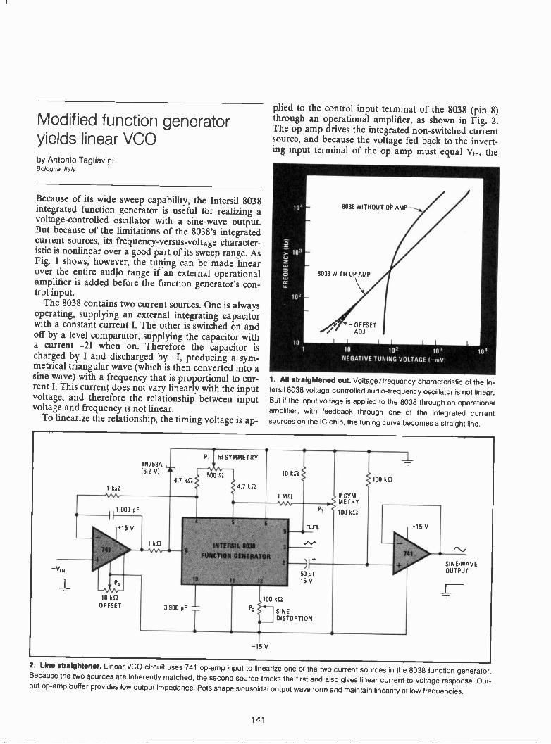
Modified function generatoryields linear VCOby Antonio TagliaviniBologna, Italy
Because of its wide sweep capability, the Intersil 8038integrated function generator is useful for realizing avoltage -controlled oscillator with a sine -wave output.But because of the limitations of the 8038's integratedcurrent sources, its frequency -versus -voltage character-istic is nonlinear over a good part of its sweep range. AsFig. 1 shows, however, the tuning can be made linearover the entire audio range if an external operationalamplifier is added before the function generator's con-trol input.
The 8038 contains two current sources. One is alwaysoperating, supplying an external integrating capacitorwith a constant current I. The other is switched on andoff by a level comparator, supplying the capacitor witha current -21 when on. Therefore the capacitor ischarged b' I and discharged by -I, producing a sym-metrical tnangular wave (which is then converted into asine wave) with a frequency that is proportional to cur-rent I. This current does not vary linearly with the inputvoltage, and therefore the relationship between inputvoltage and frequency is not linear.
To linearize the relationship, the timing voltage is ap-
plied to the control input terminal of the 8038 (pin 8)through an operational amplifier, as shown in Fig. 2.The op amp drives the integrated non -switched currentsource, and because the voltage fed back to the invert-ing input terminal of the op amp must equal Yin, the
10 10' 103
NEGATIVE TUNING VOLTAGE I mV)
1. Alt straightened out. Voltage/frequency characteristic of the In-tersil 8038 voltage -controlled audio -frequency oscillator is not linear.But if the input voltage is applied to the 8038 through an operationalamplifier, with feedback through one of the Integrated currentsources on the IC chip, the tuning curve becomes a straight line.
N
1
1 ki2
hi SYMMETRY1N753A16.2 VI A'
4.7 kSt
11,11:102_
+15 V
P4
10 kStOFFSET
1 Id/ INTERSIL 8038
FUNCTION GENERATOR
100
-15 V
SINEDISTORTION
If SYM-METRY
100 kSl
100k&2
1\d
SINE -WAVEOUTPUT
2. Line straightener. Linear VCO circuit uses 741 op -amp input to linearize one of the two current sources in the 8038 function generator.Because the two sources are inherently matched, the second source tracks the first and also gives linear current -to -voltage resporise. Out-put op -amp buffer provides low output impedance. Pots shape sinusoidal output wave form and maintain linearity at low frequencies.
141

current supplied by this source varies directly with Vin.The two integrated current generators in the 8038 areinherently matched, so the switched source tracks thenon -switched one and therefore is also linearized. Theswitched source drives a current inverter/doubler thatprovides the current -21.
The 1N753A zener diode protects the control input ofthe function generator Ic against voltages more positivethan + 0.6 volt and more negative than -6.2 v. The out-put operational amplifier is merely a buffer, and may be
omitted if low output impedance is not required.Three potentiometers permit shaping of the output
waveform. First, at a high frequency, P1 is adjusted toobtain a symmetrical wave shape (square wave frompin 9). Then P2 is set for best sinusoidal output. FinallyP3 is trimmed for good symmetry at the low -frequencyend of the tuning curve. The offset adjustment, P4, is
then adjusted to provide tuning linearity.With component values shown, the vco covers the
entire audio range (20 to 20,000 hertz).
Converter lets processordrive teletypewriterby Richard C. PascoStanford University, Stanford, Calif.
An inexpensive circuit can replace a lengthy softwareroutine at the interface between a teletypewriter and al-most any microprocessor [Electronics, July 25, 1974, p.96]. But only six integrated circuits are needed in an im-proved version that employs the standard 8 -bit ASCII
code, and only five Ics in the modification that pro-cesses the Baudot code.
This parallel -to -serial converter has many appli-cations. It will change the parallel output of a keyboardinto a serial format for transmission by telephone via a
modem, and it will interface the output of any parallel -output device with a teletypewriter for printing.
The converter's operation is easily followed with theaid of the accompanying circuit diagram. Initially theconverter is in the READY mode-that is, the BUSY flip-flop is cleared. This keeps the 16 -bit shift register in theLOAD mode and the cycle counter reset. The output ofthe shift register is held high because the parallel loadinput of its last stage is connected to Vcc.
Upon a negative -going transmission of the STROBEline, the BUSY flip-flop is set. This puts the shift registerinto the SHIFT mode, locking -in the data present at itsinputs, and removes the reset from the cycle counter.
On the first negative -going transition of the clock af-ter this strobe, the cycle counter enters state 1, andsimultaneously the shift register shifts a logic zero to itsoutput. This logic zero is the START signal.
On the next nine clocks, the shift register's outputconsists of 8 data bits and a high corresponding to the
TOMICROPROCESSOR
Vcc
ASCII DATA FROMMICROPROCESSOR
BUSY
(OR)
READY
STROBE
-L -
Vcc
Vcc
Vcc
220 Hz
AlA2A3A4A5A6
AB
SIABCREFGH
SHIFT REGISTER74185
57473
GLK CLR
READY
CLOCK
CLOCK
Vcc
A8COEFGHSHIFT REG STER
74185
+12 V
TO TELETYPEWRITER(60-mA CURRENT LOOP)
2N2222
CLE COUNTER3483
NC
Serial feed. Data from microprocessor, parallel -fed into shift register, is fed out serially to teletypewriter for printout. The STROBE and BUSY
signals synchronize the circuit with the processor. Ten characters per second are transmitted in standard 8 -bit ASCII code, but circuit is eas-
ily modified for Baudot code. This hardware eliminates a software routine for interfacing device to teletypewriter; parts cost less than $5.
142
STOP pulse. Meanwhile the cycle counter passes to states2 through 10.
The next clock puts the cycle counter into state 11,but the gate detects this and clears the BUSY flip-flop.This in turn raises the READY line, resets the cycle coun-ter, and puts the shift register back into the LOAD mode.Thus, the transition from state 10 to the READY modeproceeds asynchronously within a few nanoseconds.During this transition the shift -register output remainshigh because a logic 1 is loaded from the Vcc line.
Transmission at 10 characters per second results if anew character is provided within one clock period (9.09
ms) of this READY indication. Even if a new character isreceived immediately, however, the output will remainat 1 and transmission will not begin until the next clock.This insures a minimum stop pulse duration of twoclock periods. If no character is received, the converterwill wait in the READY mode indefinitely.
The following modifications adapt the circuit to theBaudot code. Delete the left-hand 74165, and connectthe SI and A inputs of the right-hand 74165 to VccThen replace the 7410 gate with a 7404 inverter drivenoff the 7493's D output (the A output now connects onlyto Bm; B and C outputs are left with no connection). p
Complementary JFETS formbimode oscillatorby Gregory HodowanecNewark, N.J.
A complementary pair of junction field-effect transistorscan be interconnected to form a negative -resistancetwo -terminal device, which makes a simple oscillator. Inmonolithic form this configuration is called a lambdadiode [Electronics, June 26, p. 105] and is available witha wide range of characteristics. If two discrete JFETs areconnected to make the diode, they do not have to bematched, but can be chosen to provide various values ofpeak current and negative -resistance -voltage range.Figure 1 shows current as a function of voltage for acombination consisting of an n -channel 2N3819 and ap -channel 2N5460.
The JFET "diode" can be made to oscillate at fre-quencies ranging from audio to vhf. All that is requiredis to connect the diode in series with an inductance -ca-pacitance tank circuit and supply a bias voltage in thenegative -resistance region. Figure 2 shows a simple bi-mode oscillator circuit capable of oscillating at both
iP
VP
0 2 4 6
VOLTAGF. IV)
Vv
8 10
1. Negative resistance. Current -voltage characteristics are shownfor a "diode" consisting of the arrangement of the two comple-mentary JFETS shown in Fig. 2. For any terminal voltage between2.5 V and 8 V, the combination has a negative resistance.
audio and radio frequencies simultaneously. Oscillationis at approximately the natural resonances of each tankcircuit. The radio -frequency tank, consisting of a 2-mi-crohenry choke shunted by a trimmer capacitor, can betuned over a wide range centered near 20 megahertz.The audio section uses the 500 -ohm winding of a mini-ature audio output transformer and a 0.05-microfaradceramic capacitor for oscillation at approximately 440hertz. The audio section cleanly Amplitude -modulatesthe rf section, as demonstrated by reception of the radi-ated signal on a communications receiver. Power outputis in the order of 25 milliwatts and the signal has arange of several hundred feet with no antenna on theoscillator. The range can be extended to several thou-sand feet with a short length of antenna, so a form ofthis oscillator can be adapted to radio -control appplica-tions.
This circuit can be used as a simple signal source formany experimental purposes. The audio section can beeliminated or shorted out if an unmodulated signal isdesired. The circuit can also be adapted to any designrequiring a low-level signal source. Variable frequencycontrol can be incorporated at either or both frequencylevels.
1=1
3819.CHANNEL)
CATHODE
ANODE
2N5460(p -CHANNEL)
rf TANK2µH
Jr3 - 25 pF
0.05 µF
6V
ANTENNA
af TANK
500 -OHMWINDINGOF AUDIOTRANS-FORMER
2. Bimode oscillator. JFET-combination "diode" and two tank circuits can oscillate at audio frequency and radio frequency simultaneously. Resultant signal is rf modulated by af; either componentcan be varied for communications or control applications.
143
IC timers controldc -dc convertersby P. R. K. ChettyIndian Scientific Satellite Project, Bangalore, India
An integrated -circuit timer such as the MC1455 can beused as the control element in a simple dc -to -dc conver-ter regulator. Shown below are a current step-up con-verter regulator and a polarity -reversing voltage step-upconverter regulator. Both are regulated to within 0.5%for load currents of 300 milliamperes, and have a rippleof less than 5 mA.
In these circuits the MC1455 operates as an astablemultivibrator, turning the pass transistor on and off tokeep the output -filter capacitor charged to the desiredoutput voltage. Overvoltage is prevented by a feedbackarrangement that turns off the multivibrator when thecapacitor voltage reaches a predetermined level.
The astable -mode connection of the timer causes thevoltage across capacitor C1 to oscillate between Vcc/3
and 2 Vcc/3 at a frequency of approximately1.44/(R1 + R2)Ci-about 1.3 kilohertz. The maximumoperating voltage of the timer is 16 volts, but here itsVcc is clamped at 8.2 v by zener diode Dz1. The inputvoltage therefore can have any value within the ratingsof the pass transistor and the filter capacitor.
Figure 1 shows the current step-up converter regu-lator. When the output of the control timer is high, tran-sistor Q2 is turned on and therefore pass transistor Q3 is
turned on. Collector current from Q3 flows through in-ductor L into the load and the filter capacitor. When theoutput of the timer goes low, the transistors turn off.
Diode D commutates the current flow flowing throughthe inductor when Q3 switches off. If there were nofeedback circuit, the output voltage would depend uponthe input voltage and the duty cycle.
The feedback circuit consists of R4, zener diode DZ2,
transistor Qi, and R3, Whenever the output voltage ex-ceeds (Vz2 + VBE1), Qi turns on and drives the reset ter-minal of the 1455 low. The transistors Q2 and Q3 there-fore stay off, allowing the output voltage to decrease.Thus the output voltage V0t is maintained approxi-mately equal to (Vz1 + VeE1).
The performance of the circuit in Fig. I is as follows:
VIN = 15 V
021
1N756A(8.2 VI
R3
10 k2
a,2N2222
R4
0221N756A(8.2 VI
4.7 kS2
C,
I0.1 pF
153470 12R7
270 0
R8
12012
A64.7 kit
HEAT SINK
032N4903
4e2N2222
1N5804X
VOUT V27 + VBE1
-- 8.4 V
1 mH
C
56 NF
25 V
AL.
VIN = 15 V
0Z1
1N756A(8.2 VI
a,
0z7
1N967(18 V)
R4
4.7 kS2
HEAT SINK
03
2N4903
Vour - -(VZ2 VBE1)= -19.4 V
ON1N5804
I L
1 mH-4
C
+ 400 pF35 V
1. Converted and regulated. Dc -to -dcconverter includes IC timer for regulation.The MC1455, connected as free -runningmultivibrator, switches 03 on and off. If out-
put gets too high, feedback circuit drivestimer reset low to hold switch off. Regulationis less than 0.5% at 300 mA, and ripple isless than 5 mA. Output voltage is lower thaninput voltage, so current can be stepped up.
2. Polarity reversed. Positions of inductor,commutating diode, and feedback elementsare changed here for negative output volt-age. This circuit arrangement can step upmagnitude of either voltage or current; com-ponents chosen here provide voltage step-up. Regulation is same as before.
144

Input voltage, yinOutput voltage, VoutLoad current, lout
= 15v= 8.4 v= 300 mA
Ripple, Ir (for lout = 300 mA) = 5 mALoad regulation (for Vu, = 15 v and Iout = 0-300mA) equals or is less than 0.5%Line regulation (for Vi = 15-25 v and lout = 300mA) equals or is less than 2.5%
The polarity -reversing circuit of Fig. 2 differs fromFig. I in the arrangement of L, C, D, and the feedbackelements. When Q3 switches off, the commutating cur-rent in L charges C to produce an output voltage that isnegative with respect to ground. This voltage is applied
to the anode of Dz2 through limiting resistor R4. When-ever the output is more negative than -(Vz2 + \Tam),the timer reset goes low, allowing the voltage across thecapacitor to become less negative. The output voltage ofthis circuit is therefore maintained at approximately-(Vz2 + VBEi). This circuit can provide an output volt-age equal to, less than, or greater than the input voltage.
The performance of the circuit in Fig. 2 is as follows:Input voltage, Vi = + 15 vOutput voltage, Vout = -19.4 vLoad current, Iout = 300 mA
Ripple and regulation are the same as in the earlier ex-ample.
111
Discriminator displaysfirst of four responsesby John S. FrenchWestern Electric Co., Inc., Sunnyvale, Calif.
A first -response discriminator, which turns on a light in-dicating the first switch to close and simultaneouslylocks out the other switches, can be useful in sports,games, behaviorial learning studies, and experiments inphysical science. The circuit shown here indicates whichof four switches closes first. It uses three low -drainc-mos integrated circuits and a 9 -volt radio battery.
When the push -to -close switches Si through S4 areopen, inputs D1 through D4 to the 4042 quad latch arelow. Therefore outputs Qi through Q4 are low, and Qithrough 04 are high. These four high inputs to NAND
gate G1 make Gi low and G2 high. The high outputfrom G2 is applied to the clock input of the latch; withthe clock thus enabled, the outputs of the latch can fol-low the inputs.
If switch Si is closed, D1 goes high and therefore Qigoes high, allowing light -emitting diode LEDs to light.Simultaneously, Qi goes low, sending G1 high but 02and the clock input of the latch low. The clock low locksthe latch so that D2, D3, and D4 no longer control Q2,Q3, and Q4. As a result, even if S2, S3, or S4 is closed, thecorresponding LED does not light.
The circuit is reset by momentary closing of the resetswitch to set G2 and clock high. If Si through S4 areopen, Qi through Q4 go low for the next trial.
Expansion of this circuit to handle N inputs isstraightforward. Only two NAND gates are required, butone of them must have N inputs.
4
4
CD4042AELATCH
7
D, a,
2 n2
a,
04
POLARCLOCK ITY
1
+9 V a R3 R2
ALL 1 MO,
04
2
3
10
11
CD4049AE
1k3 ---L-t>0--V\A"--141---
1 kS25 '---4))0*--14-0
9
15
+9 V
2 3 4 5 CD4012AE
14
+9 V
G,
10 119
11
14
1kS2 14
C>012
5 +9V
LED3
+9 V
+9 V
0 0
RESET
L E 4
Who's on first? The first switch to close lights up its associated LED, and blocks all other LEDs from lighting if their switches are closed. Circuit can distinguish first -closed switch for time differences as small as 0.05 microsecond. Cost of parts for entire circuit is under $10.
145

Delay line in shift registerspeeds m -sequence generationby J.T. HarveyAmalgamated Wireless (Australasia) Ltd., North Ryde, Australia
The clock rate of a shift -register generator of maximal -length pulse sequences is significantly increased when adelay line replaces one or more of the register's stages.High-speed m -sequences, as maximal -length pulse se-quences are called, are needed for testing data links, forgenerating repeatable pseudo -noise, and in spread -spectrum techniques [Electronics, May 29, p. 127].
Repetitive sequences of pulses can be generated byconnecting the output of a shift register back to the in-put in some way, setting in some initial condition that isnot all zeroes, and turning on the clock. In this situation,the length of the repeating pulse sequence that emergesfrom the register depends upon the feedback arrange-ment and perhaps upon the initial condition-if the reg-ister has N stages, the sequence may repeat after onlytwo, N, or some other number of pulses.
However, the m -sequence is independent of the start-ing condition. This follows from two facts. First, itslength is 2N - 1 pulses (the all -zero condition never ap-pears in the register). Second, its generation involves ev-ery possible combination of 1 s and Os in the shift regis-ter except for the all -zero combination.
A typical m -sequence generator is shown in Fig. 1.The feedback signal in the four -stage device is obtainedby taking the exclusive-oR (x0R) of the outputs fromthe last and next -to -last flip-flop stages. The resultingsequence repeats after (24 - 1) bits, i.e., 15 bits. It goes1, 1, 0, 0, 0, 1, 0, 0, 1, 1, 0, 1, 0, 1, 1, and then repeats.Various feedback combinations must be used to achievethe maximum -length pulse sequence from registers withvarious numbers of stages, but it is of interest to note
1. Maximizes. Four -stage shift register with feedback arrangementcycles through all possible states except the all -zero condition, pro-ducing an output sequence of 24 - 1 pulses. This is the maximum -
length sequence (m -sequence) from a four -stage register. Speed of
the m -sequence is limited by the propagation delay in the XOR gate.
that generators having 2, 3, 4, 6, 7, or 15 stages can op-erate by feeding back the XOR of the outputs from thelast and next -to -last stages.
The limit to high-speed operation of this device oc-curs when the interval between clock pulses is less thanthe combined effective propagation delay in a shift -reg-ister stage and the XOR gate. For a given family of logic,the propagation time of the XOR is typically slightly lessthan that of a shift -register stage. Thus, the clock rate atwhich an m -sequence generator can operate is typically0.5 to 0.7 of the rate at which the shift register can oper-ate alone.
Provided that operation is required over a limitedrange of clock frequency (most are operated at a fixedclock rate), then the first stage of the shift register canbe removed and a delay line substituted. This arrange-ment is shown in Fig. 2. The optimum delay is the inter-val between clock pulses less the exclusive-oR-gatepropagation delay. The gate and delay line thus simu-late a delay -free gate and one shift -register -stage delay.The maximum frequency of operation is then the max-imum shifting rate of the flip-flops.
To demonstrate this idea, some experiments wereconducted with MECL III logic, for which 270 -mega-hertz flip-flop clock rate and 2.7 -nanosecond gate pro-pagation time worst -case figures are claimed. A pair ofMC1670L D -type flip-flops were connected in a ringcounter, which was observed to operate to 310 wiz. Thesame shift -register was used in a two -stage m -sequencegenerator with the addition of an MC 1672L XOR gate,one section of which was used as an output buffer. Atthis point, the maximum clock rate was found to beonly 215 MHz. Then this generator was converted to athree -stage device by the addition of a 20 -cm length of50 -ohm coaxial cable, and satisfactory operation wasobserved in the range from 220 to 310 MHz, giving aspeed improvement of up to 44%.
The susceptibility of the circuit to noise will be great-est near these speed limits. When a 90 -cm length ofcable was used, four -stage operation was observed in
2. Faster. In modified m -sequence generator a delay line simulatesone stage of the shift register, so the output pulse sequence is the
same as for the circuit of Fig. 1. The delay line is designed so it, plusthe XOR gate, offers the same propagation delay as one registerstage, permitting a 44% increase in clock rate for the m -sequence.
146
the range from 245 to 310 MHz, and a 220 -cm lengthgave six -stage operation (63 -bit sequence) at fre-quencies from 265 to 310 MHz. Similarly, 260 cm of co-axial cable yielded a seven -stage 127 -bit sequence forclocks from 275 to 310 MHz.
For a given number of stages, an increase in the ex-
ternal delay decreases the upper and lower clocks inroughly the same ratio, while an increase in the numberof simulated stages decreases the range in the clock rate.At least one shift -register stage must be used in front ofthe first feedback tap to eliminate the possibility ofspurious oscillation.
Memory, peripherals sharemicroprocessor address rangeby James A. KuzdrallCando, N H
Designers find that the direct addressing mode of theM6800 microprocessor and similar devices cannot bebeaten for convenience and efficiency. This mode allowsthe user to directly address the lowest 256 bytes in themachine-the bytes in locations 0 through 255.
Instructions that use the mode consist of one byte todesignate the operation to be performed, plus a secondbyte to designate the address of the operand. By con-trast, other addressing modes have to supply one bit foreach of the 16 lines of the memory bus and therefore re-quire a two -byte address for the operand. Thus the di-rect -addressing mode saves one byte, or 33% of pro-gram memory space, in each instruction.
Usually the designer sets aside a portion of the RAMfor the easily accessed locations 0-255. However, it isalso convenient to assign some of these locations to theperipheral -interface adapter chips that interface the mi-croprocessor to peripheral equipment. The reason isthat, in applications requiring a large amount of datainput and output, the addresses of the PIA chips may beas active as the RAM addresses.
The circuit arrangement shown in the accompanyingdiagram allows the direct addressing range of memorylocations to be used for both random-access memoryand peripheral interface adaptors with a minimum ofhardware. It provides control for RAM in locations0-239, PIAS in locations 240-255, and ROM in locations1,024-4,095. Although the decoding is not complete be-cause address lines A8, A9, Al2-A15 are not fully de-coded, the decoding does prevent two devices frombeing active on the data bus simultaneously.
In the circuit, decoding an address to reach RAM or aPIA requires only two integrated circuits-a 74LS10triple NAND gate and a 74LS139 dual decoder.
Gate Ulf; enables the decoder when valid memory -address data is present and the data is stable (ct.2 fromclock U10 is high). Then address lines A10 and An of thecentral processing unit are decoded to make one of the2Y outputs low. Decoder outputs 2Y1, 2Y2, and 2Y3
each select a 1 -kilobyte section of ROM, i.e. Rom -1,Rom -2, or Rom -3. If both A10 and An are low, however,so that 2Y0 is low, the RAM and interface adapters areenabled. RAM -1, U4, is selected if the address is below128 (A7 low). U5 is enabled for addresses between 128and 255 (A7 high), but inhibited by gate U1A for ad-dresses 240-255.
To activate the interface adapters (U6 -U9) for theseunused addresses, the inhibit signal is inverted by Uic.The decoder outputs 1Y0 -1Y3 of U2 provide the finalselection among the interface adapters. The decodingmeets all worst -case timing and loading requirements.
The table shows the contents of the microprocessoraddress locations for this circuit arrangement. The se-lection of devices addressed is shown only as an ex-ample. For instance, more RAM can easily be added inmemory locations 256-511 using the enable inputs ofthe MCM6810L- I devices. Unneeded ROM chips, RAM
CONTENTS
Startingaddress
OF MICROPROCESSOR
Finishingaddress
Chip
ADDRESS LOCATIONS
Contents
0 127 U4 RAM -1 Random-access memory
128 239 U5 RAM -2 Random-access memory
240 U6 PIA -1 Data register A
241 - U6 PIA -1 Data register B
242 - U6 PIA -1 Control register A
243 U6 PIA -1 Control register B
244 U7 PIA -2 Data register A
245 U7 PIA -2 Data register B
246 U7 PIA -2 Control register A
247 U7 PIA -2 Control register B
248 U8 PIA -3 Data register A
249 U8 PIA -3 Data register B
250 U8 PIA -3 Control register A
251 U8 PIA -3 Control register B
252 U9 PIA -4 Data register A
253 U9 PIA -4 Data register B
254 Ug PIA -4 Control register A
255 Ug PIA -4 Control register B
1024 2047 U,1 ROM -1 Read-only memory, program
2048 3071 U12 ROM -2 Read-only memory, program
3072 4087 U13 ROM -3 Read-only memory, program
4088 4095 U,3 ROM -3 Restart and interrupt vectors
147

Us
MA -3
chips, and PIA chips can be deleted, of course.When using the configuration as shown, the pro-
gramer should initialize the stack pointer to location239 and locate the restart vector and interrupt vectors inthe last addresses of Rom -3 (U13).
U7
PERIPHERAL INTERFACE
ADAPTER -2
U3 - U10: MOTOROLAOR EQUIVALENT
U11 U13: INTEL 1-K X 8 -BITPROGRAMABLE ROMOR EQUIVALENT
usMC6828 MA -1
M 11
U13
ROM -3
U5
RANDOM-ACCESS MEMORY -21,374.
11374LS10
MCM68101-1
18 8101t.7,'
RAM -1
+5 V
1112
READ-ONLY MEMORY -2
r
U1, 2708
ROM -1
)- )- N N esi 1.4
02
74LS139 DECODER< Om<NNN
1/374LS10
tr, .10, In NCOaaa a° a .1 1 1'4 ?r
U3 MC6800
CENTRAL PROCESSING UNIT
1.110
MC NAOSCILLATOR/
CLOCKDRIVER
*1
02
02
Versatile. This circuit arrangement allows both random-access memory and peripheral interface adapters to be addressed in direct -address-ing -mode locations of M6800 microprocessor. This is convenient in operations with lots of data input and output. Logic gates enable the de-
coder for valid stable addresses and enable or disable the RAM and PIA sections. Lines A2 and Al are decoded for final selection of PIA.
148
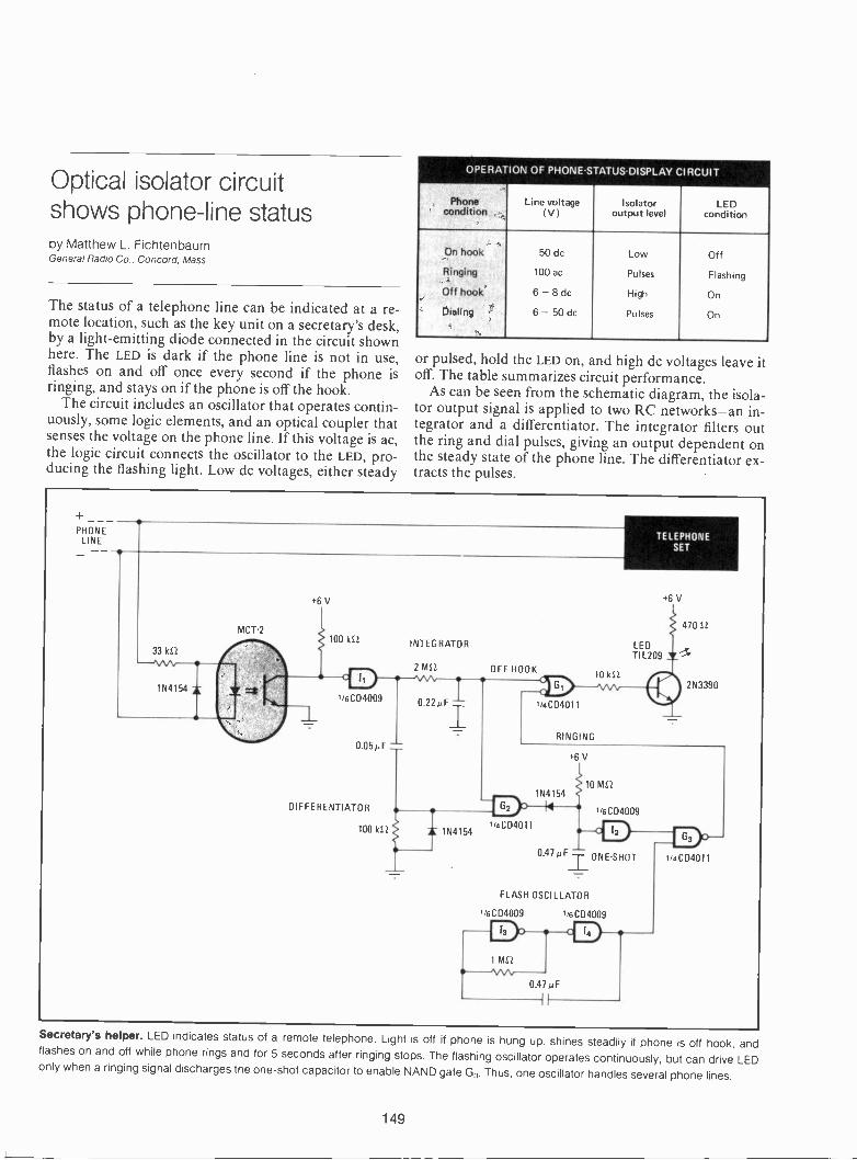
Optical isolator circuitshows phone -line statusby Matthew L. FichtenbaumGeneral Radio Co., Concord, Mass.
The status of a telephone line can be indicated at a re-mote location, such as the key unit on a secretary's desk,by a light -emitting diode connected in the circuit shownhere. The LED is dark if the phone line is not in use,flashes on and off once every second if the phone isringing, and stays on if the phone is off the hook.
The circuit includes an oscillator that operates contin-uously, some logic elements, and an optical coupler thatsenses the voltage on the phone line. If this voltage is ac,the logic circuit connects the oscillator to the LED, pro-ducing the flashing light. Low dc voltages, either steady
OPERATION
Phonecondition
OF PHONE -STATUS
Line voltageIV)
-DISPLAY CIRCUIT
Isolatoroutput level
LEDcondition
On hook
Ringing
Off hook
Dialing
50 dc
100 ac
6 - 8 dc
6 - 50 dc
Low
Pulses
High
Pulses
Off
Flashing
On
On
or pulsed, hold the LED on, and high dc voltages leave itoff. The table summarizes circuit performance.
As can be seen from the schematic diagram, the isola-tor output signal is applied to two RC networks-an in-tegrator and a differentiator. The integrator filters outthe ring and dial pulses, giving an output dependent onthe steady state of the phone line. The differentiator ex-tracts the pulses.
PHONELINE
33 kS2
MCT 2
+6 V
100 1(12
1 6004009
0 05pF
DIE FERENTIATOR
100 kl2
INTEGRATOR
2 MS2 OFF HOOK
0 22p F
1 40040111N4154
10 k12
4004011
RINGING
LEDTIL209
T ONE SHOT
FLASH OSCILLATOR
'6004009 1/6004009
1 MS2
0.47pE
+6 V
470 52
2N3390
1 / 4 C04011
Secretary's helper. LED indicates status of a remote telephone. Light is off if phone is hung up, shines steadily if phone is off hook, andflashes on and off while phone rings and for 5 seconds after ringing stops. The flashing oscillator operates continuously, but can drive LEDonly when a ringing signal discharges the one-shot capacitor to enable NAND gate G3. Thus, one oscillator handles several phone lines.
149

When the phone is on the hook, so that inverter II haslow input and high output, G1 is deactivated and can-not turn the transistor or LED on.
When the phone rings, the high dc from II and thehigh output from the differentiator combine to activate
allowing the one-shot capacitor to discharge and en-able G3. Thus the output from the flash oscillator is ap-plied to G1, flashing the LED. Flashing continues duringthe slow charge -up of the 0.47-microfarad one-shot ca-pacitor between rings and after ringing stops.
When the phone is off the hook, II has high input andlow output, so GI is able to turn on the transistor andlet the LED light. The momentary high -voltage pulsesthat occur during dialing are suppressed by the integra-tor, so G2 is not enabled.
The 100-v ac ringing signal might apply excessive re-verse voltage to the light -emitting diode in the opticalcoupler. Therefore, the coupler input is shunted by aprotecting 1N4154 diode.
Because the flash oscillator operates continuously, itcan be connected to the NAND gates G3 associated witha number of different phone lines and LEDs. In the au-thor's office, one oscillator is used for 10 phones.
This circuit uses ordinary c-mos ICs and operatesfrom a noncritical supply voltage between 5 and 10volts. The ac adapter from a pocket calculator is a con-venient source. A single power supply can handle all ofthe phone lines.
The signals that are developed at the integrator anddifferentiator outputs can be used for other purposesthan lighting a LED. Other areas of application includeplaying a recorded message when a phone rings, or run-ning a timer while a phone is in use.
This circuit does not draw appreciable current fromthe phone line, feed back to the line, or reference anyvoltages to the line because the coupling is optical.Nonetheless, the telephone company should be con-sulted before the circuit is installed. CI
Microprocessor convertspot position to digitsby John M. SchuleinAeronutronic Ford Corp.. Palo Alto. Calif.
A few bytes of program in an 8008/8080 micro-processor, plus a 555 integrated -circuit timer, can con-vert the position of a potentiometer into a digital value.The arrangement is both economical and convenientwhen the position data is an input to a system alreadyusing the microprocessor, such as an industrial controlsystem or a video game.
As the figure shows, a strobe pulse from the micro-processor' triggers a 555 connected as a one-shot multi -vibrator. The output from the 555 stays high for a pe-riod of time that is proportional to the resistance of thepot. To measure this time period, the processor incre-ments an internal register for as long as its input (D7)from the 555 remains high.
When data on the pot position is required, the micro-processor program calls up the POTPOS subroutine,which uses four flags, the accumulator, and the B regis-ter. In this subroutine, as the table shows, the processor:
1. Sets register B to 0.2. Triggers the 555.3. Increments register B.4. Inputs the status of the 555 to bit D7 of the ac-
cumulator.5. Sets a sign flag minus if status is high.6. Jumps back to step 3 if flag is minus.7. Returns to main program if flag is not minus.
Upon return to the main program, register B contains anumber that measures the 555 output pulse durationand hence is a digital representation of the pot position.
STATUS TOMICROPROCESSOR(D7)
TRIGGER FROMMICROPROCESSOR 0`(OUTPUT STROBE)
PROGRAM SUBROUTINE
POTPOS: MVI B, 0
OUT TRIGGER
CONT: INR B
IN STATUS
ANA A
JM CONT
RET
(SETS SIGN FLAG)
NOTE: Register B contains the pot position on exit.
Where is the pot? Potentiometer position is digitized by one-shotmu(tivibrator and subroutine for the 8008/8080 microprocessors.When program calls subroutine, processor triggers one-shot andmeasures output pulse duration (which is proportional to resistanceof pot). Register B stores this value for use in computation of nextstep in a TV game, process control, etc.
When the hardware and software are used on an 8008system with a 2.5 -microsecond clock, the B register dig-ital output varies from 2 to 65 Hex, i.e., has 100 differ-ent values, as the potentiometer is varied across itsrange. The values of the pot and the timing capacitorcan be modified to suit the speed of the processor andthe desired range of the digitized output. El
150
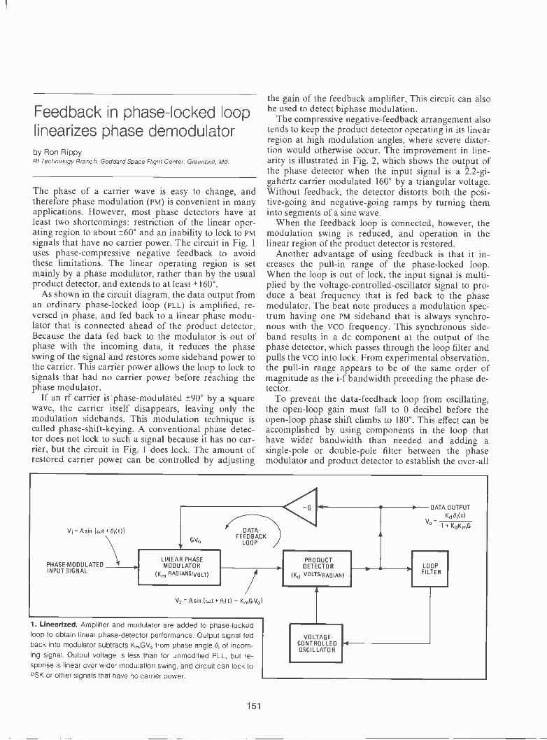
Feedback in phase -locked looplinearizes phase demodulatorby Ron RippyRI Technology Branch, Goddard Space Flight Center, Greenbelt, Md.
The phase of a carrier wave is easy to change, andtherefore phase modulation (PM) is convenient in manyapplications. However, most phase detectors have atleast two shortcomings: restriction of the linear oper-ating region to about ±-60° and an inability to lock to PMsignals that have no carrier power. The circuit in Fig. 1
uses phase -compressive negative feedback to avoidthese limitations. The linear operating region is setmainly by a phase modulator, rather than by the usualproduct detector, and extends to at least ± 160°.
As shown in the circuit diagram, the data output froman ordinary phase -locked loop (PLL) is amplified, re-versed in phase, and fed back to a linear phase modu-lator that is connected ahead of the product detector.Because the data fed back to the modulator is out ofphase with the incoming data, it reduces the phaseswing of the signal and restores some sideband power tothe carrier. This carrier power allows the loop to lock tosignals that had no carrier power before reaching thephase modulator.
If an rf carrier is phase -modulated ±90° by a squarewave, the carrier itself disappears, leaving only themodulation sidebands. This modulation technique iscalled phase -shift -keying. A conventional phase detec-tor does not lock to such a signal because it has no car-rier, but the circuit in Fig. 1 does lock. The amount ofrestored carrier power can be controlled by adjusting
the gain of the feedback amplifier., This circuit can alsobe used to detect biphase modulation.
The compressive negative -feedback arrangement alsotends to keep the product detector operating in its linearregion at high modulation angles, where severe distor-tion would otherwise occur. The improvement in line-arity is illustrated in Fig. 2, which shows the output ofthe phase detector when the input signal is a 2.2-gi-gahertz carrier modulated 160° by a triangular voltage.Without feedback, the detector distorts both the posi-tive -going and negative -going ramps by turning theminto segments of a sine wave.
When the feedback loop is connected, however, themodulation swing is reduced, and operation in thelinear region of the product detector is restored.
Another advantage of using feedback is that it in-creases the pull -in range of the phase -locked loop.When the loop is out of lock, the input signal is multi-plied by the voltage -controlled -oscillator signal to pro-duce a beat frequency that is fed back to the phasemodulator. The beat note produces a modulation spec-trum having one PM sideband that is always synchro-nous with the vco frequency. This synchronous side -band results in a dc component at the output of thephase detector, which passes through the loop filter andpulls the vco into lock. From experimental observation,the pull -in range appears to be of the same order ofmagnitude as the i-f bandwidth preceding the phase de-tector.
To prevent the data -feedback loop from oscillating,the open -loop gain must fall to 0 decibel before theopen -loop phase shift climbs to 180°. This effect can beaccomplished by using components in the loop thathave wider bandwidth than needed and adding asingle -pole or double -pole filter between the phasemodulator and product detector to establish the over-all
Vi = A sin [wt +0(01
PHASE MODULATEDINPUT SIGNAL
-0\4,
LINEAR PHASEMODULATOR
RADIANS/VOLT)
DATA -FEEDBACK
LOOP
V2 = A sin kat + (3,(t) - KmGVo)
1. Linearized. Amplifier and modulator are added to phase -lockedloop to obtain linear phase -detector performance. Output signal fedback into modulator subtracts K,GN/c, from phase angle Oi of incom-ing signal. Output voltage is less than for unmodified PLL, but re-sponse is linear over wider modu.ation swing, and circuit can lock toPSK or other signals that have no carrier power.
PRODUCTDETECTOR
(Kd VOLTS/RADIAN)
DATA OUTPUT!QO(t)
V° KdKrnG
VOLTAGE -CONTROLLEDOSCILLATOR
LOOPFILTER
151

2. What you see is what you get. Effect of data -feedback loop onlinearity is shown in scope photo. Top trace shows triangular voltagethat modulates incoming 2.2-GHz carrier. Lower traces show de-tected angle without feedback (curved) and with feedback (linear).
data -loop bandwidth. If any sharp filtering is needed, itshould be done ahead of the phase modulator. Then thedata -loop bandwidth can be left rather wide to ensure aflat frequency response without degrading the phase -detection performance in the presence of noise.
Figure 3 shows the linear phase modulator that wasused to implement the circuit for the test in Fig. 2. Thismodulator is useful at vhf and higher frequencies. (Asimilar modulator with a 3 -dB hybrid in place of the cir-culator has been used at frequencies as low as 500 ki-
= A sin (wt+0;
0V
10 V
G V)
CIRCULATORTRAK 1410 1340
3. Modulator. The linear phase modulator that is part of Fig. 1 can
be realized at vhf and higher frequencies by use of a circulator and avariable reactance. Reflected signal in port 2 changes phase as volt-
age on back-to-back varactors changes.
lohertz.) The carrier enters port 1 of the circulator andtravels to port 2, which is terminated in an LC combina-tion that is voltage -tuned by two varactor diodes. Be-cause this termination is purely reactive, all of theenergy at port 2 is reflected to the rf-output port.
The angle of the reflected carrier varies with the mod-ulating signal applied to the diodes. One modulator sec-tion of this type will produce about ±90° of linear mod-ulation. Two. sections were cascaded to produce the±160° phase shift in Fig. 2.
PROV converts binary codeto drive 1 1/2 -digit displayby V.R. GodboleNorth Electric Co., Gabon, Ohio
In providing visual readouts for test circuits, inspectionequipment, error indicators, and the like, it is often nec-essary to go from a machine -generated 4 -bit binarycode to a 11/2 -digit display of the numbers 0 to 15. Thisprocess is usually performed in two steps, but a pro-gramable read-only memory can handle it in one.
In the usual approach, the first step is to convert thebinary code into a BCD code by any one of the severalavailable techniques. The second step is to use standardBCD seven -segment decoder/driver integrated circuitsto drive the popular seven -segment visual readouts. ThePROM, however, can be programed to accept the binaryinput signals and generate the proper outputs to drivethe display directly.
This use of a PROM has several advantages. Conver-sion and driving are done in one step, thus providing di-rect interface to the visual display. Blanking and lamp -test can be included at no extra cost. Space is conserved,and cost is competitive with other approaches.
Binary coding of the numbers from 0 to 15 requires
+5V0
MAN -727 -SEGMENTDISPLAYS
12)
16
Y1
B10
A Y2 w.32 x 8
B Y3PROM82
12 4
C Y4B4
1374188
Y5ORB8
E N8223 Y6LAMP TEST
INHIBIT5 7
G Y7
Y8
a a
If bi If0
bi
dCl
ledcI
abcdefg abcde g
180 S2(81
Here's how. PROM drives seven -segment display to show decimalvalue of 4 -bit input signal. This compact interface is convenient inmicroprocessor circuits, which often have spare PROM capacity. A32 -by -8 -bit PROM can provide the drive signals for numbers 0through 15 and also accommodate lamp -test and inhibit commands.Applications include test -number indication in small test instruments
and display of settings on binary -output touch switches.
152
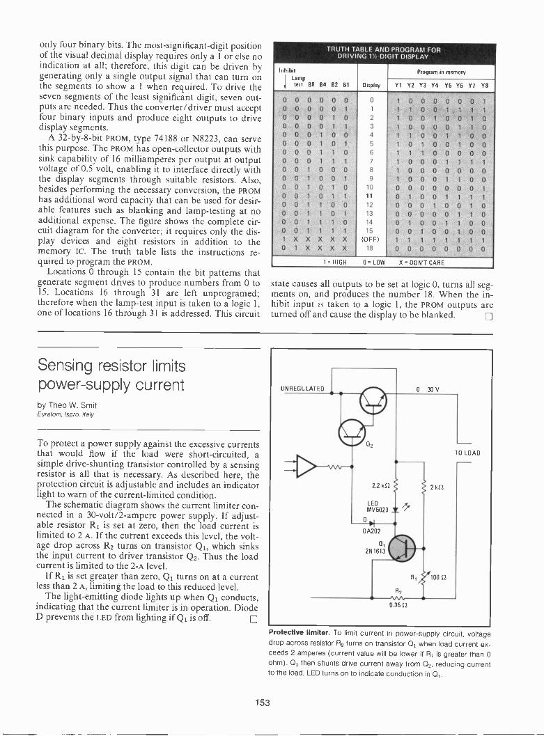
only four binary bits. The most -significant -digit positionof the visual decimal display requires only a 1 or else noindication at all; therefore, this digit can be driven bygenerating only a single output signal that can turn onthe segments to show a I when required. To drive theseven segments of the least significant digit, seven out-puts are needed. Thus the converter/driver must acceptfour binary inputs and produce eight outputs to drivedisplay segments.
A 32 -by -8 -bit PROM, type 74188 or N8223, can servethis purpose. The PROM has open -collector outputs withsink capability of 16 milliamperes per output at outputvoltage of 0.5 volt, enabling it to interface directly withthe display segments through suitable resistors. Also,besides performing the necessary conversion, the PROMhas additional word capacity that can be used for desir-able features such as blanking and lamp -testing at noadditional expense. The figure shows the complete cir-cuit diagram for the converter; it requires only the dis-play devices and eight resistors in addition to thememory ic. The truth table lists the instructions re-quired to program the PROM.
Locations 0 through 15 contain the bit patterns thatgenerate segment drives to produce numbers from 0 to15. Locations 16 through 31 are left unprogramed;therefore when the lamp -test input is taken to a logic 1,one of locations 16 through 31 is addressed. This circuit
TRUTH TABLE AND PROGRAM FORDRIVING 1% DIGIT DISPLAY
InhibitLamp
test B8 B4 82 81 Display
Program in memory
Y1 Y2 Y3 Y4 Y5 Y6 Y7 Y8
0 0 0 0 0 0 0 0 0 0 0 0 00 0 0 0 0 1 0 00 0 0 0 0 2 0 0 0 0 00 0 0 0 3 0 0 0 0 00 0 0 0 0 4 0 0 0 00 0 0 0 5 0 0 0 0 00 0 0 0 6 0 0 0 0 00 0 0 7 0 0 0
0 0 0 0 0 8 0 0 0 0 0 0 00 0 0 0 9 0 0 0 0 00 0 0 0 10 0 0 0 0 0 0 00 0 0 11 0 0 0
0 0 0 0 12 0 0 0 0 0 0
0 0 0 13 0 0 0 0 0 0
0 0 0 14 0 0 0 0 0
0 0 15 0 0 0 0 0 0
(OFF)0 18 0 0 0 0 0 0 0 0
1 = HIGH 0 = LOW X = DON'T CARE
state causes all outputs to be set at logic 0, turns all seg-ments on, and produces the number 18. When the in-hibit input is taken to a logic 1, the PROM outputs areturned off and cause the display to be blanked.
Sensing resistor limitspower -supply currentby Theo W. SmitEuratom, Ispro, Italy
To protect a power supply against the excessive currentsthat would flow if the load were short-circuited, asimple drive -shunting transistor controlled by a sensingresistor is all that is necessary. As described here, theprotection circuit is adjustable and includes an indicatorlight to warn of the current -limited condition.
The schematic diagram shows the current limiter con-nected in a 30-volt/2-ampere power supply. If adjust-able resistor R1 is set at zero, then the load current islimited to 2 A. If the current exceeds this level, the volt-age drop across R2 turns on transistor Qi, which sinksthe input current to driver transistor Q2. Thus the loadcurrent is limited to the 2-A level.
If R1 is set greater than zero, Qi turns on at a currentless than 2 A, limiting the load to this reduced level.
The light -emitting diode lights up when Qi conducts,indicating that the current limiter is in operation. DiodeD prevents the LED from lighting if Qi is off.
UNREGULATED 0 30 V
o.0 LOAD
2.2 4(S!
LEDMV5023
0A202
D,
2N1613
R2
210.0
100 S.1.
0.35 S2
Protective limiter. To limit current in power -supply circuit, voltagedrop across resistor A2 turns on transistor 01 when load current ex-ceeds 2 amperes (current value will be lower if IR1 is greater than 0ohm). 01 then shunts drive current away from Q2, reducing currentto the load. LED turns on to indicate conduction in Q.
153

Scope display of eight signalshelps debug sequential logicby Matthew L. FichtenbaumGeneral Radio Co., Concord, Mass.
When debugging sequential logic, an engineer mayhave to observe several signals simultaneously. Logicalstates and the times that they change are of primary im-portance in the visual display; the exact values of volt-age levels and the duration of rise times and fall timesare of lesser importance.
Two, four, or eight digital signals can be displayed onone of the two channels of a Tektronix 454 or similar
dual -trace oscilloscope, as demonstrated in the photo-graphs on the next page. The other channel may thenbe used for triggering or for observation of a ninth sig-nal. The eight signals are treated as logic levels and aregated by a digital multiplexer. Although this proceduredoes not preserve voltage levels and wave shapes, itdoes achieve maximum speed with simple circuitry.
The circuit for displaying the signals on the scope isillustrated in Fig. I. The 7493 divide -by -16 counter (U3)is incremented after each scope sweep. The countersteps through the eight inputs sequentially, and the ex-tra stage compensates for the use of every other sweepin the "alternate" display mode. The counter's highestthree bits select an input signal via digital multiplexerU 1, which is a 74S151 TTL Schottky type. At the sametime, the CD4051 c-mos analog multiplexer U2 picks adc voltage off a resistor chain. This voltage is summed
DIGITAL -SIGNALINPUTS
2
3
4
5
6
7
+5 V
0.22µF
I
16
DIGITAL MULTIPLEXER
+5 V ANALOG MULTIPLEXER
+5 V
0.22µF
120 S2(9)
16
+5 V
200 St
+5 V
2 pF
0.001 µF = 100S2
560 E213)
Si
S2
TO SCOPECHANNEL -2INPUT
500 E2
SEPARATION
11
+5 V
10
FROM SWEEPQ GATE A OF
SCOPEi)
200 St
14
COUNTER
1. Multi -trace adapter. Two, four, or eight digital input signals time-share the channel -2 trace of a dual -trace oscilloscope by means of thiscircuit. The digital multiplexer selects individual digital inputs in cyclic succession, and the analog multiplexer separates their wave forms ver-tically; sweep counter drives multiplexers. Switches S1 and S2 permit display of only two or four digital wave forms, instead of eight.
154
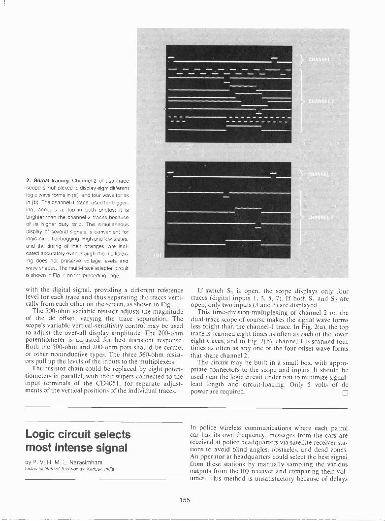
2. Signal tracing. Channel 2 of dual -tracescope is multiplexed to display eight differentlogic wave forms in (a) and four wave formsin (b). The channel -1 trace, used for trigger-ing, appears at top in both photos; it is
brighter than the channel -2 traces becauseof its higher duty ratio. This simultaneousdisplay of several signals is convenient forlogic -circuit debugging. High and low states,and the timing of their changes, are indi-cated accurately even though the multiplex-ing does not preserve voltage levels andwave shapes. The multi -trace adapter circuitis shown in Fig. 1 on the preceding page.
with the digital signal, providing a different referencelevel for each trace and thus separating the traces verti-cally from each other on the screen, as shown in Fig. 1.
The 500 -ohm variable resistor adjusts the magnitudeof the dc offset, varying the trace separation. Thescope's variable vertical -sensitivity control may be usedto adjust the over-all display amplitude. The 200 -ohmpotentiometer is adjusted for best transient response.Both the 500 -ohm and 200 -ohm pots should be cermetor other noninductive types. The three 560 -ohm resist-ors pull up the levels of the inputs to the multiplexers.
The resistor chain could be replaced by eight poten-tiometers in parallel, with their wipers connected to theinput terminals of the CD4051, for separate adjust-ments of the vertical positions of the individual traces.
If switch S1 is open, the scope displays only fourtraces (digital inputs 1, 3, 5, 7). If both SI and S., areopen, only two inputs (3 and 7) are displayed.
This time -division -multiplexing of channel 2 on thedual -trace scope of course makes the signal wave formsless bright than the channel -1 trace. In Fig. 2(a), the toptrace is scanned eight times as often as each of the lowereight traces, and in Fig. 2(b), channel 1 is scanned fourtimes as often as any one of the four offset wave formsthat share channel 2.
The circuit may be built in a small box, with appro-priate connectors to the scope and inputs. It should beused near the logic circuit under test to minimize signal-lead length and circuit -loading. Only 5 volts of dcpower are required.
Logic circuit selectsmost intense signalby P. V. H. M. L. NarasimhamIndian Institute of Technology, Kanpur, India
In police wireless communications where each patrolcar has its own frequency, messages from the cars arereceived at police headquarters via satellite receiver sta-tions to avoid blind angles, obstacles, and dead zones.An operator at headquarters could select the best signalfrom these stations by manually sampling the variousoutputs from the HQ receiver and comparing their vol-umes. This method is unsatisfactory because of delays
155
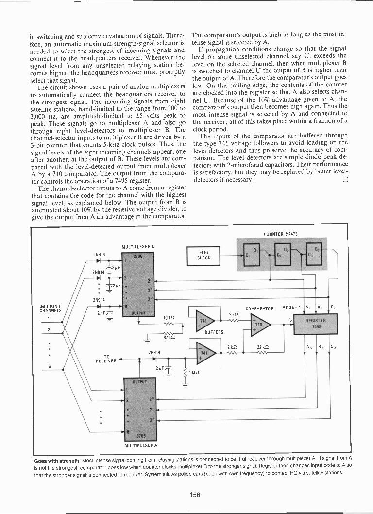
in switching and subjective evaluation of signals. There-fore, an automatic maximum -strength -signal selector isneeded to select the strongest of incoming signals andconnect it to the headquarters receiver. Whenever thesignal level from any unselected relaying station be-comes higher, the headquarters receiver must promptlyselect that signal.
The circuit shown uses a pair of analog multiplexersto automatically connect the headquarters receiver tothe strongest signal. The incoming signals from eightsatellite stations, band -limited to the range from 300 to3,000 Hz, are amplitude -limited to ±5 volts peak topeak. These signals go to multiplexer A and also gothrough eight level -detectors to multiplexer B. Thechannel -selector inputs to multiplexer B are driven by a3 -bit counter that counts 5 -kHz clock pulses. Thus, thesignal levels of the eight incoming channels appear, oneafter another, at the output of B. These levels are com-pared with the level -detected output from multiplexerA by a 710 comparator. The output from the compara-tor controls the operation of a 7495 register.
The channel -selector inputs to A come from a registerthat contains the code for the channel with the highestsignal level, as explained below. The output from B isattenuated about 10% by the resistive voltage divider, togive the output from A an advantage in the comparator.
The comparator's output is high as long as the most in-tense signal is selected by A.
If propagation conditions change so that the signallevel on some unselected channel, say U, exceeds thelevel on the selected channel, then when multiplexer Bis switched to channel U the output of B is higher thanthe output of A. Therefore the comparator's output goeslow. On this trailing edge, the contents of the counterare clocked into the register so that A also selects chan-nel U. Because of the 10% advantage given to A, thecomparator's output then becomes high again. Thus themost intense signal is selected by A and connected tothe receiver; all of this takes place within a fraction of aclock period.
The inputs of the comparator are buffered throughthe type 741 voltage followers to avoid loading on thelevel detectors and thus preserve the accuracy of com-parison. The level detectors are simple diode peak de-tectors with 2-microfarad capacitors. Their performanceis satisfactory, but they may be replaced by better level -detectors if necessary.
INCOMINGCHANNELS
1
2N914
01
2N914 2111
T.T.2µF
2N914
1_2µFl.
MULTIPLEXER B
37051
2
8
OUTPUT
2°
21
22
5 -kHz
CLOCK
aCl
COUNTER '0473
a,C3
10 k52
MA.
171\'--(11
741
BUFFERS
2 kC2
2 kS-2
COMPARATOR
710
22 kS2
MODE = 1 A
REGISTER
7495
2N914TO
741
RECEIVER
1 MI?.
OUTPUT
20
21
2
3705
MULTIPLEXER A
Ao B 0 co
Goes with strength. Most intense signal coming from relaying stations is connected to central receiver through multiplexer A. If signal from A
is not the strongest, comparator goes low when counter clocks multiplexer B to the stronger signal. Register then changes input code to A so
that the stronger signal is connected to receiver. System allows police cars (each with own frequency) to contact HQ via satellite stations.
156
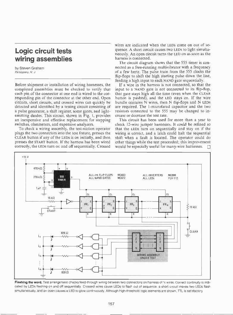
Logic circuit testswiring assembliesby Steven GrahamParsippany, N. J.
Before shipment or installation of wiring harnesses, thecompleted assemblies must be checked to verify thateach pin of the connector at one end is wired to the cor-responding pin of the connector at the other end. Opencircuits, short circuits, and crossed wires can quickly bedetected and identified by a testing circuit consisting ofa pulse generator, a shift register, some gates, and light -emitting diodes. This circuit, shown in Fig. 1, providesan inexpensive and effective replacement for steppingswitches, ohmmeters, and expensive analyzers.
To check a wiring assembly, the test -station operatorplugs the two connectors into the test fixture, presses theCLEAR button if any of the LEDs is on initially, and thenpresses the START button. If the harness has been wiredcorrectly, the LEDs turn on and off sequentially. Crossed
wires are indicated when the LEDs come on out of se-quence. A short circuit causes two LEDs to light simulta-neously. An open circuit turns the LED on as soon as theharness is connected.
The circuit diagram shows that the 555 timer is con-nected as a free -running multivibrator with a frequencyof a few hertz. The pulse train from the 555 clocks theflip-flops to shift the high starting pulse down the line,feeding a high input to each NAND gate sequentially.
If a wire in the harness is not connected, so that theinput to a NAND gate is not connected to its flip-flop,that gate stays high all the time (even when the CLEARbutton is pushed), and the LED stays on. If the wirebundle contains N wires, then N flip-flops and N LEDs
are required. The 1-microfarad capacitor and the tworesistors connected to the 555 may be changed to in-crease or decrease the test rate.
This circuit has been used for more than a year tocheck 12 -wire jumper harnesses. It could be refined sothat the LEDs turn on sequentially and stay on if thewiring is correct, and a latch could halt the sequentialshift when a fault is located. The operator could doother things while the test proceeded; this improvementwould be especially useful for many -wire harnesses.
+15 V
470 k1-2
270 kE2 555TIMER
ALL J K FLIP-FLOPS MC663 ALL INVERTERS MC680ALL NAND GATES MC672 ALL LEDs FLV-112
1 µ F
-:- CL
.____CL CL CL
15 kitJ J Q
.......J at1A.A, 1> n-+-
FF1 FF2
--ip-FF3
-J 0
FFN
K ti K O K 5 K§ 15 kt2
_START.R R
FI CLEAR
820 St1 1Lt -Hit-AAA-O.< on_2 2
--7
3
4 s
3. . .
L2 . . .4..__$.-L ---14-NAA----0-ca. WIRING ASSEMBLY
UNDER TEST
Lry 40-14-,\AN--0if 820 12
-4
Flashing the word. Test arrangement checks feed -through wiring between two connectors on harness of N wires. Correct continuity is indi-cated by LEDs flashing on and off sequentially. Crossed wires cause LEDs to flash out of sequence, a short circuit makes two LEDs flashsimultaneously, and an open causes a LED to glow continuously. Although high -threshold -logic elements are shown, TTL is satisfactory.
157

Controllable current sourceeliminates matched resistorsby James A. StankoState Univesity of New York, Stony Brook, N.Y.
A bipolar constant -current source that has a groundedvoltage source and a grounded load is usually limited inaccuracy and internal impedance by the degree ofmatching of two or more resistors. For the circuit below,however, no matched resistors are required; linearityand internal impedance are determined solely by theoperational amplifier gain, offset, and power supply re-jection ratio. This circuit takes advantage of the fact
+15 V
POWERSUPPLY COM
-15 V
VIN
27 kn
RI
3 k52 R2
R3
1REF
741
2.7 kS2
R4
1k52
RL
Uncritical. Load current produced by this circuit depends on inputvoltage, not load resistance. Circuit does not require matched resis-tors for accurate control of current, but power supply must float.
that the op amp's power supply can usually be floated.To understand the operation of the circuit, remember
that no current to speak of flows into the input termi-nals of the op amp under feedback conditions, and novoltage difference exists across the terminals. Thus, theop amp drives the common terminal of the power sup-ply to the voltage level established at the inverting in-put. This voltage appears across the reference resistorR4. It is set to a suitably low value by input attenuatorR1 and R2 to avoid thermally induced errors caused bypower dissipated in the reference resistor. The values ofR1 and R2 are chosen to provide a convenient scale fac-tor. The reference current thus established is exactlyequal to the current flowing in the load, and thereforethe load current is
IL = -Iref = R4 R1 + R2
The value of load current does not depend upon thevalue of load resistance and can be controlled by thevalue of Vin.
The minus sign in the expression for load current in-dicates the degenerative feedback action of the circuit.If IL increases, the extra voltage drop through R4 drivesthe noninverting input of the op amp lower and thusdecreases the output.
Resistor R3 is made equal to the parallel combinationof R1 and R2 to minimize any error caused by inputbias current. For the values shown in the figure, inputvoltages up to ± 10 volts produce current outputs up to±10 milliamperes.
This circuit has been used for over a year to supplycurrent to electromagnets. In this application it isboosted by an emitter follower for greater output cur-rent and more voltage compliance. 0
Vin R2
Graduated -scale generatorcalibrates data displayby Ken E. AndersonIBME University of Toronto, Canada
Scope and chart displays may require reference sig-nals to indicate timing or counting scales. The circuitshown here is added to the display portion of a real-time digital data correlator at a cost of $3 or $4 to pro-vide a graduated scale below the correlation display ona two -channel scope. Although it lacks the precision of acursor, the continuous scale offers greater versatility andspeed of operation. It also references the display datawhen stored on hard copy.
The photographs in Fig. 1 show two scales that can be
generated to aid the observer in determining the pulsecount or time at which a wave form rises or falls. In thelower trace of Fig. 1(a), every fifth clock pulse is indi-cated, and in Fig. 1(b), every second clock pulse is indi-cated. The upper trace in each photo shows.a wave formthat goes high at count 20, low at 40, high again at 70,low again at 90, and so forth. These counts can be readeasily and accurately from the reference scales.
As shown in Fig. 2, the scale generator is remarkablysimple. For two decades of unique graduations, twodecade counters (7490) and one package of open -collec-tor AND gates (7409) are required. These gates switch acrude voltage -divider digital -to -analog converter, gen-erating the various pulse heights. Gate A in Fig. 2 ANDSthe system clock with the basic scale unit-five in Fig.2(a) or two in Fig. 2(b)-enabling the voltage -divideroutput to rise. Low gates B, C, or D (or combinations)clamp the output to appropriate levels as determined byR1, R2, R3, and R4. As higher -order counters progres-
158
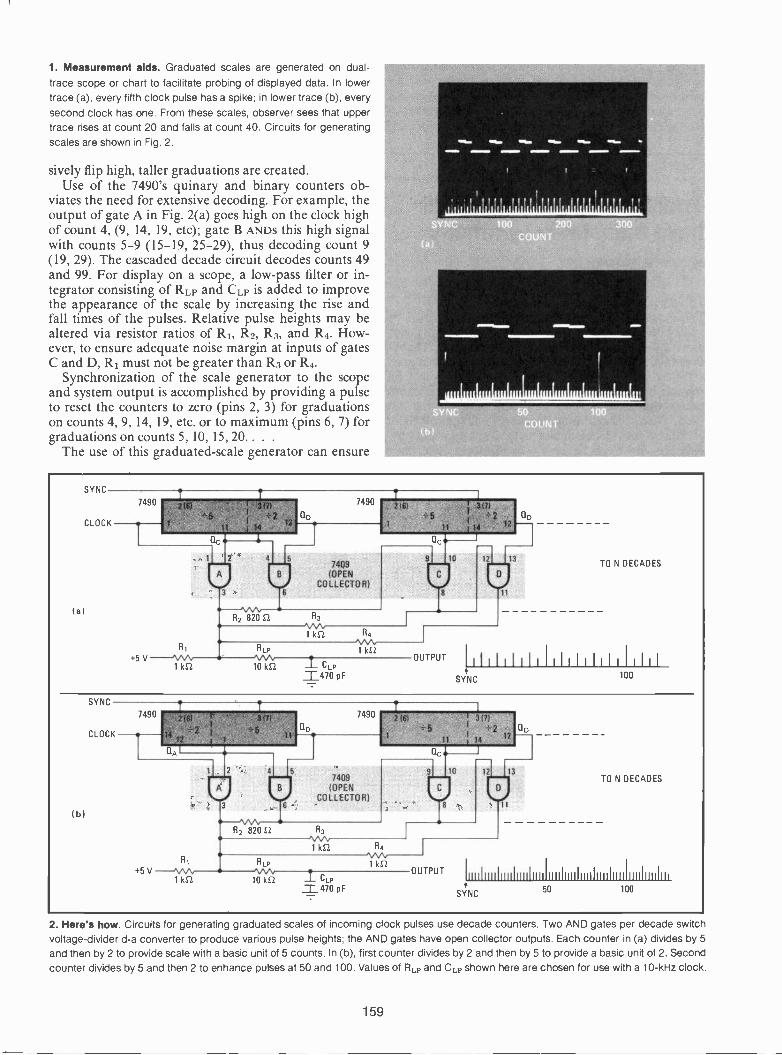
1. Measurement aids. Graduated scales are generated on dual -trace scope or chart to facilitate probing of displayed data. In lowertrace (a), every fifth clock pulse has a spike; in lower trace (b), every
second Clock has one. From these scales, observer sees that uppertrace rises at count 20 and falls at count 40. Circuits for generatingscales are shown in Fig. 2.
sively flip high, taller graduations are created.Use of the 7490's quinary and binary counters ob-
viates the need for extensive decoding. For example, theoutput of gate A in Fig. 2(a) goes high on the clock highof count 4, (9, 14, 19, etc); gate B ANDS this high signalwith counts 5-9 (15-19, 25-29), thus decoding count 9(19, 29). The cascaded decade circuit decodes counts 49and 99. For display on a scope, a low-pass filter or in-tegrator consisting of RLp and CLp is added to improvethe appearance of the scale by increasing the rise andfall times of the pulses. Relative pulse heights may bealtered via resistor ratios of R1, R2, R3, and R4. How-ever, to ensure adequate noise margin at inputs of gatesC and D, R1 must not be greater than R3 or R4.
Synchronization of the scale generator to the scopeand system output is accomplished by providing a pulseto reset the counters to zero (pins 2, 3) for graduationson counts 4, 9, 14, 19, etc. or to maximum (pins 6, 7) forgraduations on counts 5, 10, 15, 20. . . .
The use of this graduated -scale generator can ensure
' ' I
SYNC
CLOCK
(a)
SYNC
CLOCK
(b)
1 2
R2 820 SZA,
1 k52
RLP
1 kS2+5 V
7490
R4
1k1-2
10 kS0
2 4 5
CLP
470 pF
7409(OPEN
COLLECTOR)
R2 820 11 N3
'w\.1k12
R1RLP
+5 V
R4
"V\A,1k5-2
1 kSZ 10 kS1 CLPM470 pF
9 10 12 13
11
TO N DECADES
OUTPUT 1
1 1 1 1 1 1 1 1 1 1 1 1 1 1 1 1 1 1 1 1 I 1
SYNC 100
up
12 13TO N DECADES
OUTPUT111111111111111111111111111d111111111111111111111111111111111
SYNC 50 100
2. Here's how. Circuits for generating graduated scales of incoming clock pulses use decade counters. Two AND gates per decade switchvoltage -divider d -a converter to produce various pulse heights; the AND gates have open collector outputs. Each counter in (a) divides by 5and then by 2 to provide scale with a basic unit of 5 counts. In (b), first counter divides by 2 and then by 5 to provide a basic unit of 2. Secondcounter divides by 5 and then 2 to enhance pulses at 50 and 100. Values of R. and Cup shown here are chosen for use with a 10 -kHz clock.
159
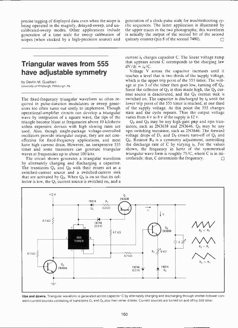
precise tagging of displayed data even when the scope isbeing operated in the magnify, delayed -sweep, and un-calibrated-sweep modes. Other applications includegeneration of a time scale for sweep calibration ofscopes (when clocked by a high -precision source) and
generation of a clock -pulse scale for troubleshooting cy-clic sequences. The latter application is illustrated bythe upper traces in the two photographs; this waveformis actually the output of the second bit of the secondquinary counter (pin 8 of the second 7490).
Triangular waves from 555have adjustable symmetryby Devlin M. GualtieriUniversity of Pittsburgh, Pittsburgh, Pa.
The fixed -frequency triangular waveform so often re-quired in pulse -duration modulators or sweep gener-ators too often turns out costly to implement. Thoughoperational -amplifier circuits can develop a triangularwave by integration of a square wave, the tips of thetriangle become blunt at frequencies above 10 kilohertzunless expensive devices with high slewing rates areused. Also, though single -package voltage -controlledoscillators provide triangular output, they are not cost-effective for fixed -frequency applications, and mosthave high current drain. However, an inexpensive 555timer and some transistors can generate triangularwaves at frequencies up to about 100 kHz.
The circuit shown generates a triangular waveformby alternately charging and discharging a capacitor.The transistors Qi and Q2 with their zeners act as aswitched -current source and a switched -current sinkthat are activated by Q3. When Q3 is on so that its col-lector is low, the Qi current source is switched on, and a
current it charges capacitor C. The linear voltage rampthat appears across C corresponds to the charging lawdV/dt = i1/C.
Voltage V across the capacitor increases until itreaches a level that is two thirds of the supply voltage,which is the upper trip point of the 555 timer. The volt-age at pin 3 of the timer then goes low, turning off Q3.Since the collector of Q3 is thus made high, the Qi cur-rent source is deactivated, and the Q2 current sink isswitched on. The capacitor is discharged by i2 until thelower trip point of the 555 timer is reached, at one thirdof the supply voltage. At this point the 555 changesstate and the cycle repeats. Thus the output voltagevaries from 4 v to 8 v if the supply is 12 v.
Qi and Q2 may be any high -gain pop and npn tran-sistors, such as 2N3638 and 2N3646. Q3 may be anynpn switching transistor, such as 2N3646. The forwardvoltage drops of D1 and D2 ensure turn-off of Qi andQ2. Resistor R2 is a symmetry adjustment, controllingthe discharge rate of C by varying i2. For the valuesshown, the frequency in hertz of the symmetricaltriangular wave form is roughly 75/C, where C is in mi-crofarads; thus, C determines the frequency. 9
4.7 0.1
+12 V
1N914 R1
4.7 kt2
D, 2.2 kS2
a,2N3638
555TIMER
1N746(3.3 V)
4.7 kS7.
03
2N3646
4.7 kSZ
1N746(3.3 V) rt
C12
2N3646
5k$2
1N914
02
Ups and downs. Triangular waveform is generated across capacitor C by alternately charging and discharging through emitter -follower constant-current sources consisting of transistors Qi and Q2 plus their zener diodes. Current sources are turned on and off by 555 timer.
160
Inverting dc -to -dc convertersrequire no inductorsby Craig Scott and R.M. StittBurr -Brown Research Corp., Tucson, Ariz.
Many systems require a modest negative power sourcewhere only a positive power supply is available. Such anegative voltage can be produced by an inverting dc -to -
dc converter installed right where it is needed. This ar-rangement is especially convenient in systems where thedc power is supplied remotely because only two wiresneed to be run to the point of use, instead of three. Theinverting dc -to -dc converter described here requires noexpensive transformers or inductors. Noise spikes asso-
ciated with switching inductive loads are therefore elim-inated.
To understand the operation of the circuit, considerfirst the -5-volt converter shown in Fig. 1. Resistor R1,capacitor C1, and two inverters form a free -running100 -kilohertz oscillator. The remaining four inverters inthe hex -inverter package form a power driver. On thepositive swing at the output of the power driver, C2 ischarged through diode D1 and transistor Qi (assumingthat Qi is on). When the output of the power driverdrops back to zero, D1 reverse -biases and D2 forward -biases, so charge is transferred to C3.
As the cycle repeats, C3 is charged to a negative volt-age that approaches the positive -output swing minusthe diode drops, power -driver drop, and the drop acrossQi. Qi is held on by R2 until the base -drive current isshunted away by the breakdown of Dz1. This occurswhen the negative output voltage exceeds the break -
EACH INVERTER IS1/6 OF A 740901
OSCILLATOR
Cl
220 pF
D
1N914
a,2N3904
C2
1µF
+15 V
14
74C901
1N914
1N5232(5.6 V)
C3
-5-VOUTPUT
-5 3
-5.1
-4 9
-4.7
LINE REGULATIONAT low. = 15 mA
10 12 14 16
VOLTAGE IN (VI-5.2
-5.00
o-4.8
70
50
30
10 641111110 5 10 15 20 25 30 35
CURRENT OUT (mA)
MENEM11111111111111
IILOAD REGULATIONAT VIN = 15 V II
MEMO=5 10 15 20 25 30 35
CURRENT OUT (mA)
RIPPLE VS LOADAT VIN = 15 V
1111,1111
1. Converts and Inverts. Dc -to -dc converter provides inverted regulated output of -5 volts without use of transformer or inductor. Instead, itputs negative potential on C3 by discharge of C2 during off -cycle of oscillator. Performance curves show data for typical units.
161

EACH INVERTER IS1/6 OF A 74C901
OSCILLATOR
Cl
220 pF
D
1N914
2N3904
C2
1µF
1N914
+15 V
R2
10 kS2
+15 V
14
74C901
1N914
1N5246(16 V)
7
1N914
-15-VOUTPUT
C5
1µF
15
LINE REGULATIONAT louT = 5 mA
10 12 14
VOLTAGE IN (V)16
-15.2
I LI I15 1
15.0
0
35
AT Viry = 15 VRIPPLE VS LOAD
LOAD REGULATIONAT ViN = 15 V
25
15
5 FIA10 5 10
CURRENT OUT (mA)
5 10
CURRENT OUT (11A)15
15
2. More volts. Addition of voltage -multiplier stage to circuit in Fig. 1 allows it to deliver a regulated output of -15 V. These inverting -converter
circuits are convenient for producing negative voltages at locations remote from the main positive power source
down voltage rating of Dz1, less the VBE of Q. Thus,the output voltage is regulated at \Tout = -(Vzi - VBE).
With the output loaded, the negative output voltageof this circuit evidently cannot exceed that of the posi-tive power -supply input in size. It is possible, however,to modify the circuit so that it produces a negative volt-age equal to or larger than the input voltage. By addinga voltage -multiplier stage to the circuit of Fig. 1, for in-stance, the maximum possible output voltage can bedoubled.
Such a circuit is shown in Fig. 2, in which C4 ischarged through D3 on the positive swing of the power -
output stage. However, now C4 is charged from the neg-ative voltage that appears at the negative terminal ofC3. The voltage across C4 then approaches twice the in-put voltage, minus the drops. This voltage is transferredto the output capacitor as before. The negative -outputvoltage can therefore approach twice the input voltage,less the drops. [I]
Photocoupler provides agcfor audio communicationsby Richard K. DickeyCalifornia Polytechnic State University, San Luis Obispo, Calif.
In all communications systems that have speech input,some form of automatic gain control is desirable tomaintain the optimum signal level despite wide vari-ations in the amplitude of the input level. To eliminatefluctuations caused by varying transmission efficiency,agc is also desirable at the receiving terminal.
A good agc system should introduce no amplitude orfrequency distortion and should have a fast attack and a
162

1. Agc amplifier. Photoresistor in optical coupler provides feedbackpath for operational amplifier circuit in (a); output signal drives LEDto reduce photoresistance and thus reduce gain. Transfer character-istics are shown in (b); 0 dBm is taken as 0.775 volt rms. The lowerlimitation on agc is shown by the curved portion of the characteristicat low input levels. Gain approaches unity at high input levels.
moderately slow decay. The circuit of Fig. 1(a), whichhas all these features, can reduce an input variation inexcess of 50 decibels to an output variation of only 16dB. This circuit uses a 741 operational amplifier con-nected in the noninverting mode. The gain of this con-figuration is 1 + RF/105, where RF is the feedbackresistance (in ohms). The feedback resistor is the photo-resistor of a CLM-6000 optical coupler.
Unlike the more common phototransistor couplers,the CLM-6000 has a photoconductive cell; op -amp out-put voltage in excess of the forward drop of the cou-pler's light -emitting diode (about 1.4 v) decreases thephotocell resistance. Therefore the 741 operates as alinear amplifier with a gain that is controlled by its ownoutput. The characteristics of the photoresistor includea quiCk drop in resistance when illuminated and a slowrecovery of resistance after darkness begins. The com-pression characteristics of the agc amplifier are shownin Fig. 1(b).
The 1N914 diode that shunts the LED completes the
OPTIONALTTL-LOGICCONTROL
(a)
1162 1N914
OUTPUT
I b)
-10
+20
+10
EVA=0
-40 -30 -20 -10 0 +10 +20
INPUT (dBm)
2. Wider range. Inverting connection of op amp (a) provides greateragc; transfer characteristics (b) show that 50 -dB variation of inputsignal produces only 12.6 -dB variation at output. The input imped-ance is less than for noninverting connection used in Fig. 1, and aconstant low driving impedance is required. Optional portion of cir-cuit shown in color allows a TTL signal to turn off output.
circuit for the negative phase of the ac signals, so thatthe 0.05-µF capacitor can discharge. The 10-megohmshunt across the photoresistor is necessary to preventloss of dc feedback and consequent output saturation inthe absence of signal. If output saturation were allowedto occur, the system would lock up, and no ac signalcould appear at the output.
For a wider dynamic range, the inverting -mode oper-ational amplifier circuit of Fig. 2(a) can be used; the in-put impedance is finite (100 kilohms), and a constantlow driving impedance is required. For large input sig-nals, the gain of this circuit goes below 1, so the circuitbecomes an attenuator.
An additional feature of this configuration is that theoutput may be effectively switched off by a transistor -
transistor -logic signal applied to the LED as shown.When the TFL signal is high, the LED emits so muchlight that the photoresistor conducts strongly and forcesthe gain to zero. When the TTL signal is low (less than0.8 v), the circuit operates normally.
163

Inductive proximity detectoruses little powerby Matthew L. FichtenbaumGeneral Radio Co., Concord, Mass.
A contactless limit switch and a tachometer pickup aretwo possible applications for the inductive proximitydetector described here. This detector changes its outputlevel from high (9 volts) to low (0 v) whenever a con-ducting object is close by. It uses less power than aphotocell pickup and is immune to environmental dustand dirt.
The sensing element is an unshielded high -Q induc-tor coil wound on a ferrite core. When a metallic objectis brought close to the inductor, eddy currents that areinduced in the metal absorb energy from the rf field ofthe coil and thus reduce its Q.
The active elements in the detector circuit are four ofthe C-MOS MOSFET5 in a CD4007A package, and two1N3604 diodes are included. FET Qi and its associated
components, together with the inductor, constitute anoscillator that operates at about 100 kilohertz. The twodiodes develop a dc voltage proportional to the peak -to -peak value of the oscillator signal. This voltage is ap-plied to a Schmitt trigger composed ic- Q2, Q, and Q4
and holds this circuit in the "on" state.A conductive object near the coil absorbs energy
from the magnetic field of the coil, so that the oscillatoramplitude drops. The rectified voltage therefore drops,and the Schmitt trigger turns off. The variable resistoradjusts the oscillator's operating level and hence its sen-sitivity to metal objects.
The inductor used in this circuit consists of 150 turnsof #34 enameled wire inside half of a Ferroxcube 1811-PL00-3B7 pot core set, as shown in the figure. The in-ductance is approximately 2 millihenries. The circuitcan detect the presence of metal objects at distances upto a centimeter from the open end of the coil.
This circuit draws about 250 microamperes at 9 v. Itmay be used to drive c-mos logic directly or to drive abuffer that in turn drives TTL.
150 -TURN COIL
INDUCTORDETAILS
HALF OFFERROXCUBE1811 -PLO 0-3B7
CORE SET
Qi -(14 PART OF CD4007 PACKAGECIRCLED NUMBERS ARE CD4007 PINSCONNECT PIN 14 TO VDD
VDD(+9 VI
ID-- OUTPUTiz (NORMALLY
HIGH; GOESLOW TOINDICATEMETALOBJECT)
Detects metal. Proximity detector consists of modified Colpitts oscillator, amplitude detector, and Schmitt trigger. Ou-put signal is normally
high; but when oscillator coil is loaded by presence of metal object, amplitude decreases and output from Schmitt trigger goes low. Detail
drawing shows construction of the oscillator coil in a proximity detector that serves as the noncontacting pickup for a tachometer.
164

Low -distortion oscillatoruses state -variable filterby Walter G. JungForest Hill, Md.
The state -variable filter, which in any case excels as aflexible active -filter design block, can also be made tooscillate with only a little additional circuit complexity.With high-performance quad op amps now readilyavailable, a single integrated circuit makes a ultra -low-distortion sine -wave oscillator with a output frequencyof up to 5 kilohertz and three output phases for drivingservo or instrumentation systems.
The schematic diagram shows the circuit of the os-cillator. Operational amplifiers A1, A2, and A3 comprisethe state -variable filter, with its normal negative feed-back path via R4; positive feedback to sustain oscilla-
tion is provided by R6. The oscillation frequency isgiven by:
f = 1/27 RC
where R is the value of equal resistors R5 and R7 and Cis the value of equal capacitors C1 and C2. For the cir-cuit shown, f is 1 kilohertz.
As in other sine -wave oscillators, the positive andnegative feedback paths must be carefully balanced toattain-and sustain-low-distortion operation. The bal-ance is achieved by use of some type of automatic gaincontrol; in this circuit the mechanism is the variablechannel resistance of field-effect transistor Qi.
The agc circuit in itself comprises an active loop thatserves several important purposes. The integrator A4 fil-ters and smoothes the rectified output to provide a dccontrol voltage for the gate of Qi. Low ripple on thiscontrol voltage is necessary to prevent modulation dis-tortion on the output. The high dc gain of the integratorautomatically adjusts the loop to the required dc biasfor Qi in spite of parameter variations, thus eliminating
R2
A/VN.,10 kS1
C3I 10 pF
R6
82 k11
113 10 kIL
Al
470 E2
2N4861
'VVV10 kF2
R5
16 kSt
C1 R7
16 IcS1 0.041F
A2
C2
0.01µF
A3
-160°C
-90°
0°
C4
A4 ARE SECTIONS OFRAYTHEON 4136 OP AMPOR EQUIVALENT
R8
33 kS2
g 150 ks-2
1N914
-15 V
(REFERENCE)
1N914
+15 V
COM
-15 V
+µF1
OUTPUTS
TO PIN 11 OF OP AMP
1µF
TO PIN 7 OF OP AMP
State -variable oscillator. Addition of regenerative feedback via Re changes state -variable filter into sine -wave oscillator with three phases ofoutput. Filter uses three of the amplifiers in a quad op amp IC; the fourth amplifier is part of agc loop that ensures ultra -low distortion.
165

the necessity for device selection. The output voltage isregulated to a value that causes the average current inR8 to be equal to that in R9. Thus R9 and the -15-v sup-ply serve as a reference, and the agc loop tracks this ref-erence to maintain the output peak voltage at about 10v.
Resistors R10 and R11 provide a local feedback patharound Qi, to reduce distortion drastically below thestraightforward connection. The high values of feed-back resistance (100 kilohms) in relation to Qi's "on"resistance (nominally 100 ohms) prevent undesirable in-teraction of the ac and dc signals.
In operation, the total harmonic distortion at the A
output is on the order of 0.02%, and distortion in the Band C outputs is considerably less because of the low-pass filtering in the A2 and A3 integrator circuits. Alloutputs appear at the same level, with the phase rela-tions shown.
The prototype of this circuit uses a Raytheon 4136quad op amp, which has a 3 -megahertz bandwidth. TheHarris 4741, with similar ac characteristics, is anothersuitable unit. The Motorola 3403 and National 348,both 1 -MHz devices, provide ultra -low -distortion per-formance at frequencies up to 2 kHz. The main asset ofa quad device for this circuit is its cost-effectiveness-theentire circuit can be built for $10 or less.
Two ICs make low-costvideo -distribution ampby M. J. SalvatiSony Corp. of America, Long Island City, N. Y
For less than $25 in parts, a video distribution amplifiercan be constructed with all the features of commercialmodels selling for over $300. The circuit shown in Fig. 1takes the 1 -volt peak -to -peak output of a standard videosignal generator or TV camera and provides four ormore independent outputs that each deliver 1-v pk-pkvideo into 75 -ohm loads. Two input connectors aremounted in parallel because the 50-kilohm impedanceis high enough to permit "loop -through" connection, inwhich a second distribution amplifier is paralleled withthe first by means of the second connector. If not used
for loop -through, the second connector should be termi-nated with 75 ohms. The frequency response of the unitis flat from dc to 4 megahertz.
The video distribution amplifier circuit in Fig. 1 usesa National LM318 high-speed operational amplifierand a National LH0002CN current driver in a feedbackloop. The resulting output impedance is so low that theoutput approximates a zero -impedance voltage source,so loads connected to the output resistors have no effecton each other. The 75 -ohm output resistors provide theproper drive -source impedance for coaxial cable, short-circuit protection for the LH0002CN, and increased iso-lation between loads.
The only adjustment required is the frequency -re-sponse compensation capacitor. This trimmer is set toprovide the same output amplitude with a 1 -MHz sine -wave input as is obtained with a 10 -kilohertz sine waveinput.
The 6.8-microfarad bypass capacitors should be tan-talum electrolytics and should be installed close to the
0.05µF+6.2V
6.8µF
4_ OUTPUTS
INPUT 75 E2 1%
16V470 E2
75 E2 1%W\,
LM318 LH0002CN
0.05µF =6.8µF 75 E2 1%
+
51 kE2 16 V0.05µF
2 kS2 1% -6.2 V 75 S2 1%
2 ki2 1%
,w15-20 pF
FREQUENCYCOMPENSATION
1. Video distribution amplifier. Signal from TV camera or video signal generator is amplified to provide 1 v peak -to -peak at each of fouroutputs matched to 75 -ohm loads. Second input connector can be used for "loop -through" connection of a second distribution amplifier orfor a terminating resistor. Frequency -compensation adjustment balances stray capacitances, providing flat response from dc to 4 MHz.
166
2. Power supply. Compact supply uses zener-diode regulation toprovide ±6.2 volts required for video distribution amplifier. Thispower supply and the amplifier shown in Fig. 1 are capable of drivingmore outputs than the four shown.
3. All packed up and ready to go. Amplifier -and -power -supply unitfor 4 -way distribution of video signals is packaged in metal box. a artscost for complete assembly is less than $25.
LH0002CN pins. The 0.05-µF bypass capacitors shouldbe disk ceramics installed as close to the LM318 pins aspossible. The 75 -ohm and 2-kilohm precision resistorsmust be noninductive types, such as metal film or car-bon film.
The outstanding feature of this design is the low costof the ics implementing it. Although the slewing abilityof the LM318 is insufficient to handle reliably a 2-v pk-pk output swing at 4 MHz, the amplitude of the highest -frequency component (color burst) in a standard com-
posite video signal is only a small percentage of theoverall amplitude, so the LM318 can easily handle astandard video signal.
The power supply recommended for use with thisamplifier is shown in Fig. 2. Fig. 3 shows the completevideo distribution amplifier and power supply unitpackaged in a metal box. El
Four -bit a -d converterneeds no clockby Craig J. HartleyBaylor College of Medicine, Houston, Texas
Many analog circuits utilize digitally controlled solid-state switches or multiplexers to adjust filter roll -off,amplifier gain, and the like; and in many such cases theadjustable parameter is itself a function of some analogvoltage. As it happens, the 3 -bit or 4 -bit analog -to -dig-ital converter required in such applications can be builtfrom only three parts-a 5 -volt supply and two quadcomparators.
Other a -d converter designs generally include a coun-ter, a clock, a d -a converter, a comparator, and other as-sociated digital circuitry. In the design described here,however, the elements of one quad are used as com-parators, while the elements in the other quad serve as
buffers. The four outputs can drive TTL loads directly.In operation the state of each output bit is deter-
mined in sequence, starting with the most significantbit. The reference voltage for each bit is determined bya resistor network at the inverting input of each com-parator. The resistors are connected in a 1, 1/2,
1/4 . . . sequence to 1/2 Vref and the outputs of each ofthe more significant bits. The reference voltage for bit A(MsB) is always 1/2 Vref. For bit B the reference voltage is
Vref if bit A (MK) is low, or 'A Vref if bit A is high.The reference for bit C is 1/2, 3/8, 5/8, or 7/8 Vref, dependingon the states of bits A and B. The reference for bit D,the least significant bit, is 1/16, 3/16, . . . 15/16 Vref.To eliminate unwanted output switching on input noise,hysteresis of about 0.02 volt is provided at each refer-ence input by the 20-, 10-, 4.7-, and 2.2-megohm feed-back resistors.
The full-scale input voltage is Vref, which in this cir-cuit is approximately 3.5 v. (The 50-kilohm potentiome-ter scales down higher input voltages.) The two diodesset Vref at about 1.5 v below the 5-v supply to satisfy themaximum input conditions of the National LM339
167

ANALOGINPUTVOLTAGE
50 kS2
2.21(12
2.2 kS2
VREF -3.5 V
100 kS2
VREF /2
100 kEr
100 kS2*
100 ksr
5
100 kI2
50 kS2'
100 kS2*
25 kS2*
B
100 kS2*
COMPARATORS
2.2 kE2
20 MS2
10 MS2
2.2 kS2
4.7 MS2
2.2 kS2
2.2 MS2
NVV
1N914
9
2 2 kS2
2.2 kS2
14
BUFFERS
+5 V
MSB
LSB
DIGITALOUTPUTWORD
IC -1, IC -2 LM339N QUAD COMPARATORS *1% PRECISIO 4 RESISTORS
Four -bit a -d converter. This conversion circuit uses negative feedback to match the digital output word to the analog input voltage one bit ata time. It distinguishes 16 voltage levels between 0 and 3.5 V. This converter does not require a clock, a d -a converter, or digital signals foroperation, which makes it convenient for driving a digitally controlled switch in a system where all other elements are analog.
comparators and also to make the output voltage com-patible with TTL. The output voltage is approximately0.14 v (low) or 3.5 v (high). Because the comparator -buffer pairs are complementary (one is off while theother is on), the current through the diodes is nearlyconstant, making Viet independent of the output states.Total supply current is about 8 milliamperes.
The digital outputs track the analog input with aworst -case acquisition time equal to the sum of the
propagation delays of each comparator. This sumranges from 1 microsecond up to 5µs for the 339 com-parator, depending on the rate of change of the input. Afaster comparator would shorten the acquisition timesignificantly. Accuracy is controlled by tne matching ofthe resistors indicated by an asterisk in the figure.
Compatibility with other logic forms can be achievedby adjusting the supply voltage, \Tref, and the load re-sistors on each comparator.
168

)r stores.rtes
Jcessing, a video signal oftenfor longer than the few seconds
rectifiers. But a rectifier thatof a video signal for up to fourom two operational amplifiersling the cost and complexity of
ple-and-hold circuit.in Fig. 1, the CA3100 op ampal (between 0 and 6 volts) to thearad plastic capacitor. The out--1 amplified error signal used tostorage capacitor.
ut sections are conventional. Aiplifier, the CA3130, with thend low input bias current, acts.ietween the capacitor and the-kilohm resistor lowers the out -very high level of the 3130.
circuit is the unusual method.nto and out of the capacitor..er uses a series diode for thisliode has a reverse leakage cur-
rent that is unpredictable, temperature -dependent, andoften on the order of several nanoamperes. To avoidthis leakage, the circuit shown uses the base -collectorjunction of a pnp transistor to transfer charge. The cur-rent is injected into the emitter, with the base connectedto the output of the buffer amplifier. As a result, thebase -collector voltage is close to zero, and collectorleakage current is small.
An npn transistor is added to allow the capacitor tobe discharged. Normally, this transistor does not con-duct because its base -emitter junction is shorted by theswitch. Thus, when the switch is closed, the output volt-age (which is equal to the voltage across the capacitor)is determined by the most positive level applied to theinput terminal. When the switch is open, the outputvoltage tracks the input signal (Fig. 2).
Holding performance of the circuit is quite good. If a3-v signal is applied and removed, the output decaysless than 10 millivolts in 10 minutes. This implies thatthe total leakage current into the capacitor is less than10 picoamperes.
A drawback is the low slew rate. The minimum slewrate is set by the 10-kilohm resistors, the 0.47-p.F capaci-tor, and the difference between the maximum outputvoltage of the CA3100 and the maximum signal volt-age. With a 6-v input signal, the slew rate is about 850v/s.
Several variations on the circuit are possible. Theswitch could be replaced by an electronically controlleddevice, such as a relay or a CD4016 complementary -metal -oxide -semiconductor transfer gate. This change
2N4062
RESETSWITCH
OUTPUT
1. Stores maximum level. Peak detector circuit accepts analog input signals of 0 to 6 V in amplitude, provides output level that is maximum.
value of input. Use of pnp transistor for rectification minimizes charge leakage from capacitor, so peak level can be held for several minutes.
Switch and npn transistor allow circuit to be reset. While reset switch is open, output signal follows input signal. If the reset switch is relocatedto short the emitter to the base on the pnp transistor, the circuit is a minimum level detector, storing the lowest level of the input signal.
169
RESET SWITCH RESET SWITCHCLOSED OPEN
2. Holding the peak. Output from circuit of Fig. 1 is the highest levelthat has been applied to the input since switch was closed. If switch
is opened, output slews down to input level, and then follows input.Circuit was developed for determining dynamic range of low -band-width scanning signal from an electron microscope, but is useful forany peak rectifier that requires low decay rate.
would allow electronic control of the reset function.If the switch is moved to the emitter of the npn tran-
sistor, the circuit stores the lowest level of the input sig-nal. If switches are placed in both locations, the circuitcan function in four modes: tracking (both switchesopen), positive peak detector, minimum level detector,and holding (both switches closed).
By using both a positive peak detector and a mini-mum level detector in a circuit, maximum and mini-mum voltage levels can be stored for such purposes assetting the gains of variable -gain amplifiers, or storingthe levels of transient peaks in a signal.
Mark/space modulatordrives acoustic couplerby Jack D. DennonComputerphone Systems, Renton, Wash.
When data must be transmitted over a voice channel,the circuitry used to translate the logic lows and highsinto audio -frequency signals usually includes fre-quency -trimming potentiometers. But precise enoughmark and space audio signals can be obtained from acircuit that uses only standard resistor and capacitorvalues, provided the supply voltage is well -regulated.
The circuit shown translates serial logic -level datainto audio -frequency analog frequency -shift -keyed sig-nals for transmission by telephone, radio, or other voicechannels. The modulation function, including provisionfor a logic -level data input and an active -low enable -carrier input, is implemented with a single comple-mentary-mos 74CO2 quad NOR gate. The output buffer,which consists of gates 3 and 4 of the integrated circuit,has four n -channel transistors paralleled to ground fordriving an 8 -ohm speaker. The speaker provides acous-tic coupling to a telephone handset.
Logic low at the data input turns off transistor Qi andturns on transistor Q2. With Q2 on, C2 is switched intothe circuit. The frequency of the audio oscillator, madefrom gates 1 and 2 of the integrated circuit, is propor-tional to 1/RC where C = Ci + C2. Switching C2 intothe circuit causes the output frequency to shift fromK/RC1 to K/R(Ci + C2) where K is a constant. Withthe component values shown, K/RC1 = 1,269 hertz,and K/R(Ci + C2) = 1,052 Hz. These frequencies havebeen found to be sufficiently close to the specified 1,270-Hz mark frequency and 1,070 -Hz space frequency for re-liable transmission at a data rate of 110 bits per secondto a Bell 103 dataset.
The circuit draws about 30 milliamperes from a regu-lated 12 -volt supply. With appropriate changes in thevalues of components R, C1, and C2, supply voltagesfrom 6 to 15 v can be used.
The enable -carrier input to the modulator is drivenfrom a companion receiver circuit to complete the"handshake" sequence at the beginning of a data call;that is, the local receiver asserts the active -low enable
+12 V
1 kS2
ENABLE CARRIERLOGIC LEVELFROM LOCALRECEIVER
1 kS2
10 kS2
74CO2
0.047µF
0015µF
2N2222
INPUT OUTPUTLOGIC FREQUENCY
H 1270 HzL 1070 Hz
2
al2N2222
I 8 OHMSPEAKER
100 12
FSK OUTPUT
10 ki2.
+12 V
LOGIC -LEVEL
4.7 kS2 INPUT
FSK modulator. C-MOS quad NOR gate is audio -signal generatorand output driver/buffer for transmitting data over voice channel byfrequency -shift -keyed audio signals. The logic -level enable -carrierinput must be taken low for the modulator to operate; this input isdriven by the local receiver and is used to properly sequence the ini-tial exchange of signals called "handshaking." The enable carriershould be taken low about half a second after the dataset at theother end of the line answers the call with its 2,225 -Hz marking tone.
170
carrier shortly after it first hears the 2,225 -Hz markingtone coming from the dataset at the other end of thephone line.
Bell 103 line protocol calls for frequency -division -multiplexed simultaneous two-way transmission. Themodem originating the call sends 1,270 -Hz mark and1,070 -Hz space frequencies and receives 2,225 -Hz mark
and 2,025 -Hz space frequencies from the answeringdataset. At the beginning of the call, the answeringdataset immediately places its 2,225 -Hz mark signal onthe line. On a long-distance call, this tone should beallowed to reside alone on the line for at least 400 milli-seconds to disable any one -way -at -a -time devices (echosuppressors) on the telephone trunk lines.
Common -gate, common -basecircuits shift voltage levelsby Peter J. BungeAtomic Energy of Canada Ltd Chalk River. Ontario
The voltage -shifting interface needed between in-compatible logic systems can be quite straightforward-just a field-effect transistor in a common -gate circuit ora bipolar transistor in a common -base circuit. Both cir-cuits are fast, uncomplicated, and economical in bothparts cost and power drain.
The common -gate FET circuit shown in Fig. 1 cancouple the active outputs from any logic family to avoltage level higher than the Vic of the logic-an im-possibility with pullup resistor interfacing or comple-mentary -metal -oxide -semiconductor buffer (4009, 4010)interfacing. It uses much less power than open -collectortransistor -transistor -logic interfacing, especially when
+10 V
INPUT OUTPUT
INPUT
+5 V
470 07407 2N3640
OPEN -COLLECTORTTL
18 pF
4010 -I H- 2N3640
C-MOSBUFFER
4.7 kS2
OUTPUT
560
-10 V
OUTPUT
5.6 k0
-10 V
only one signal is involved, and it is much faster thansome commercial level shifters (e.g. 100 nanosecondsversus 900 ns for the Solitron CM410AE). For the2N4393 FET shown, the input range is 3 to 40 voltswhile the output range is 0 to 40 v (determined by thepinch -off and breakdown voltages of the device.)
The common -gate circuit provides only positive out-put voltages. A typical application is in interfacing ann-mos random-access memory, which has 0-v and 3-voutput levels, to c-mos circuitry. Interfacing is neces-sary in this case because the 3-v level is just at the oper-ating threshold of c-mos when it is operating from a 5-vsupply.
Common -base transistor circuits are used to interfacepositive voltage levels to negative -referenced logic. Fig-ure 2 shows arrangements for translating 0-v or +5-vTTL or c-mos levels to -10 v or -5 v. These methods aresimple, require little power, and can be used with eitheractive outputs or open -collector outputs, as shown.
1. Level translator. A field-ef-fect transistor in the common -gate configuration can provideoutput voltages that are higherthan the supply voltage of thedriving logic. Here the FETvoltage -shifter accepts input
levels of 0 or 3 V and deliversoutputs of 0 or 10 V. The fasttransitions and short delays
that are demonstrated in theoscilloscope photo areachieved by minimizing the
load capacitance.
2. Signal polarity Inversion.Common -base level translatorinterfaces positive voltages tonegative -referenced logic. Cir-cuits here accept levels of 0 or
5 V and deliver outputs of -10or -5 V. Waveforms shown arefor circuit driven by open -col-lector TTL. Speed is sacrificedto conserve power in the cir-cuit driven by a C-MOS buffer.The 18-pF speed-up capacitorcharges input capacitance oftransistor.
171

Dual -555 -timer circuitrestarts microprocessorby James R. BainterMotorola Semiconductor Products, Phoenix, Ariz.
If noise on one of its bus lines garbles an instruction se-quence, a microprocessor system will operate in-correctly-unless monitored by a timing circuit such asthe one described here. When the circuit detects agarble, it generates a restart signal that causes the mi-croprocessor to start its program all over again. The cir-cuit also generates the power -on starting signal for thesystem.
Take the case of the M6800 microprocessor, whichemploys instructions composed of three 8 -bit binarynumbers, or bytes. The first byte is the operation code-describing the task to be accomplished-and the secondand third bytes, if required, contain either data or ad-dress information. Now, suppose the hexadecimal num-ber 20FE is to be loaded into the index register of the
M6800. The instruction in machine code (hex represen-tation) is cE,20,FE, and the three bytes reside in threeconsecutive memory locations. If noise from one of thedata, address, or control buses were to make the proces-sor skip the CE, the next byte, 20, woLld be interpretedas the operation code for "branch always," and then thebyte FE would cause the processor to branch always onitself-in effect locking itself up in a locp with no exit.
One way of restoring proper operation is to restartthe system by pulling down the restart pin. In the caseof the MC6800, this means driving Fin 40 of its low-
voltage condition-a job done by the circuit in Fig. 1.The circuit is implemented with an MC3456 dual -
555 -type timer. Timing portion T1 and timing networksR1, C1 and R2, C2 generate a 400 -ms restart signal whenpower is applied. During normal program execution asignal lead applies a periodic pulse to T2. In Fig. 1 thispulse comes from CB2, the number 2 control lead fromsection B of a peripheral interface adapter. But if theprocessor goes off into never-never land or gets stuck ina loop with no exit, timer T2 causes T1 to generate a re-start signal.
The circuit operates as follows Assume pin 5, the out-put of Tl, is in the logic 0 (low-level) state. The pulses
+5 V
RI
1 MS2
0.33µFCl
1
C6
0.01 µF
+5 V
R3
100 ki2
100 SZ
Vcc+5 V
6
'/eMC14572
a2 to kS2
2N3903
+5 V
1/6 MC14572
C4
I
100 pF
100 kS2
9 PE RIPHE.INTERFACEADAPTER
M6820
1. Generates a fresh start. Dual -timer circuit applies starting pulse to microprocessor and also restarts it if noise bursts or other troublescause it to get off program or stuck in a loop. Improper operation is indicated by absence of timing pulse to T2 from a adapter program.
172
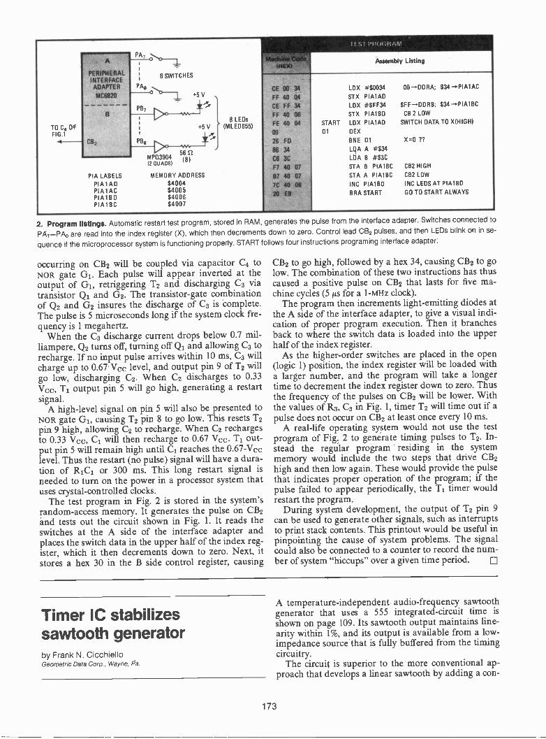
PAA
(HEXAssembly Listing
PERIPHERAL
1
,-,
,
INTERFACE I
8 SWITCHES
ADAPTER PAD CE 00 34 LOX #$0034 00 -+DDRA; $34 -,PIA1ACMC6820 +5 V ,
pg7x.'
FF 40 04CE FF 34
STX PIAIADLDX #$FF34 $FF--.DDRB; $34-.P1A18C
B FF 40 06 STX PIAI BD CB 2 LOW8 LEDs
TO C4 OF i +5 V (MLED655) FE 40 04 START LOX PIAIAD SWITCH DATA TO X(HIGH)
FIG.1 I .. 09 DI DEX
CB2 ,F10A26
FD BNE 131 X=0 ??I56 S2
86 34 LGA A #$34MP03904 (8)(2 QUADS)
C6 3C LbA B #$3CF7 40 07 STA B PIA1BC CB2 HIGH
PIA LABELS MEMORY ADDRESS 87 40 07 STA A PIA1BC CB2 LOW
PIA1AD $4004 7C 40 06 INC PIAIBD INC LEDS AT PIAIBDPIAIAC $4005PIA18D $4006 20 EB BRA START GO TO START ALWAYS
PIAIBC $4007
2. Program listings. Automatic restart test program, stored in RAM, generates the pulse from the interface adapter. Switches connected to
PA7-PAD are read into the index register (X), which then decrements down to zero. Control lead CB2 pulses, and then LEDs blink on in se-
quence if the microprocessor system is functioning properly. START follows four instructions programing interface adapter:
occurring on CB2 will be coupled via capacitor C4 toNOR gate G1. Each pulse will appear inverted at theoutput of G1, retriggering T2 and discharging C3 viatransistor Qi and G2. The transistor -gate combinationof Q2 and G2 insures the discharge of C3 is 'complete.The pulse is 5 microseconds long if the system clock fre-quency is 1 megahertz.
When the C3 discharge current drops below 0.7 mil-liampere, Q2 turns off, turning off Qi and allowing C3 torecharge. If no input pulse arrives within 10 ms, C3 willcharge up to 0.67 Vcc level, and output pin 9go low, discharging C2. When C2 discharges to 0.33Vcc, T1 output pin 5 will go high, generating a restartsignal.
A high-level signal on pin 5 will also be presented toNOR gate G1, causing T2 pin 8 to go low. This resets T2pin 9 high, allowing C2 to recharge. When C2 rechargesto 0.33 Vcc, C1 will then recharge to 0.67 Vcc. T1 out-put pin 5 will remain high until C1 reaches the 0.67-Vcclevel. Thus the restart (no pulse) signal will have a dura-tion of R1C1 or 300 ms. This long restart signal isneeded to turn on the power in a processor system thatuses crystal -controlled clocks.
The test program in Fig. 2 is stored in the system'srandom-access memory. It generates the pulse on CB2and tests out the circuit shown in Fig. 1. It reads theswitches at the A side of the interface adapter andplaces the switch data in the upper half of the index reg-ister, which it then decrements down to zero. Next, itstores a hex 30 in the B side control register, causing
CB2 to go high, followed by a hex 34, causing CB2 to golow. The combination of these two instructions has thuscaused a positive pulse on CB2 that lasts for five ma-chine cycles (5 lus for a 1-1v1Hz clock).
The program then increments light -emitting diodes atthe A side of the interface adapter, to give a visual indi-cation of proper program execution. Then it branchesback to where the switch data is loaded into the upperhalf of the index register.
As the higher -order switches are placed in the open
a larger number, and the program will take a longertime to decrement the index register down to zero. Thusthe frequency of the pulses on CB2 will be lower. Withthe values of R3, C3 in Fig. 1, timer T2 will time out if apulse does not occur on CB2 at least once every 10 ms.
A real -life operating system would not use the testprogram of Fig. 2 to generate timing pulses to T2. In-stead the regular program residing in the systemmemory would include the two steps that drive CB2high and then low again. These would provide the pulsethat indicates proper operation of the program; if thepulse failed to appear periodically, the T1 timer wouldrestart the program.
During system development, the output of T2 pin 9can be used to generate other signals, such as interruptsto print stack contents. This printout would be useful inpinpointing the cause of system problems. The signalcould also be connected to a counter to record the num-ber of system "hiccups" over a given time period. 111
Timer IC stabilizessawtooth generatorby Frank N. CicchielloGeometric Data Corp., Wayne,
A temperature -independent audio -frequency sawtoothgenerator that uses a 555 integrated -circuit time isshown on page 109. Its sawtooth output maintains line-arity within 1%, and its output is available from a low -impedance source that is fully buffered from the timingcircuitry.
The circuit is superior to the more conventional ap-proach that develops a linear sawtooth by adding a con -
173
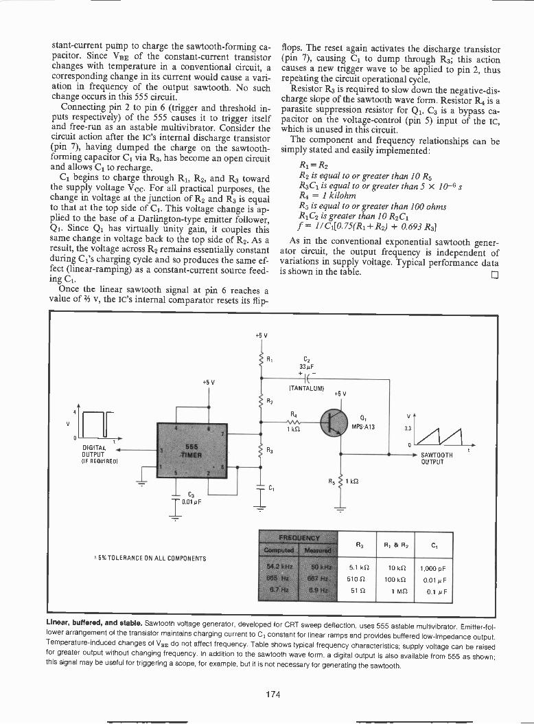
stant-current pump to charge the sawtooth-forming ca-pacitor. Since VBE of the constant -current transistorchanges with temperature in a conventional circuit, acorresponding change in its current would cause a vari-ation in frequency of the output sawtooth. No suchchange occurs in this 555 circuit.
Connecting pin 2 to pin 6 (trigger and threshold in-puts respectively) of the 555 causes it to trigger itselfand free -run as an astable multivibrator. Consider thecircuit action after the ic's internal discharge transistor(pin 7), having dumped the charge on the sawtooth-forming capacitor C1 via R3, has become an open circuitand allows C1 to recharge.
C1 begins to charge through R1, R2, and R3 towardthe supply voltage Vcc. For all practical purposes, thechange in voltage at the junction of R2 and R3 is equalto that at the top side of C1. This voltage change is ap-plied to the base of a Darlington -type emitter follower,Qi. Since Qi has virtually unity gain, it couples thissame change in voltage back to the top side of R2. As aresult, the voltage across R2 remains essentially constantduring C1's charging cycle and so produces the same ef-fect (linear -ramping) as a constant -current source feed-ing Ci.
Once the linear sawtooth signal at pin 6 reaches avalue of 3 v, the IC's internal comparator resets its flip-
flops. The reset again activates the discharge transistor(pin 7), causing C1 to dump through R3; this actioncauses a new trigger wave to be applied to pin 2, thusrepeating the circuit operational cycle.
Resistor R3 is required to slow down the negative -dis-charge slope of the sawtooth wave form. Resistor R4 is aparasite suppression resistor for Q1. C3 is a bypass ca-pacitor on the voltage -control (pin 5) input of the lc,which is unused in this circuit.
The component and frequency relationships can besimply stated and easily implemented:
R1=R2R2 is equal to or greater than 10 R5R3C1 is equal to or greater than 5 x 10⁻⁶ sR4 = 1 kilohmR5 is equal to or greater than 100 ohmsR1C2 is greater than 10 R2C1f = 1/ C1[0.75(R1+ R2) + 0.693 R3]
As in the conventional exponential sawtooth gener-ator circuit, the output frequency is independent ofvariations in supply voltage. Typical performance datais shown in the table.
V
4
0
+5 V
DIGITALOUTPUTOF REQUIRED)
±5% TOLERANCE ON ALL COMPONENTS
+5 V
SAWTOOTHOUTPUT
FREQUENCYRI & R2 C1
ComputedR3
Measured
54.2 kHz
665 Hz
50 kH 5.1 k11
667 H 510 11
51 11
10 kft
100 kS1
1 MS2
1,000 pF
0.01 i./ F
0.1 µF
Linear, buffered, and stable. Sawtooth voltage generator, developed for CRT sweep deflection, uses 555 astable multivibrator. Emitter -fol-lower arrangement of the transistor maintains charging current to C1 constant for linear ramps and provides buffered low -impedance output.Temperature -induced changes of VBE do not affect frequency. Table shows typical frequency characteristics; supply voltage can be raisedfor greater output without changing frequency. In addition to the sawtooth wave form, a digital output is also available from 555 as shown;this signal may be useful for triggering a scope, for example, but it isnot necessary for generating the sawtooth.
174
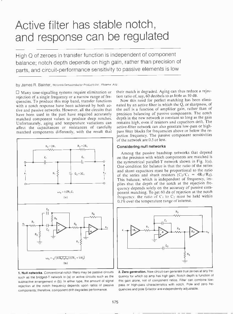
Active filter has stable notch,and response can be regulated
High Q of zeroes in transfer function is independent of component
balance; notch depth depends on high gain, rather than precision of
parts, and circuit -performance sensitivity to passive elements is low
by James R. Bainter, Motorola Semiconductor Products Inc., Phoenix, Ariz.
111 Many tone -signalling systems require elimination orrejection of a single frequency or a narrow range of fre-quencies. To produce this stop band, transfer functionswith a notch response have been achieved by both ac-tive and passive networks. However, all the circuits thathave been used in the past have required accuratelymatched component values to produce deep notches.Unfortunately, aging and temperature variations canaffect the capacitances or resistances of carefullymatched components differently, with the result that
R2 = 2R, R2 = 2R,
Cl C1
1e, R C2 = 2Ci
I
wN = 1/213,C,
(a)
C4
R1
-IR5
R6
R8 -C3 PIIOIII'
R
-:-R
-11°.e0
L'iN = v/(1/R5C3C4)(1/R, + 1/R2)
(b)
1. Null networks. Conventional notch filters may be passive circuitssuch as the bridged -T network in (a) or active circuits such as thesubtractive arrangement in (b). In either type, the amount of signalrejection at the notch frequency depends upon ratios of passivecomponents; therefore, component drift degrades performance.
their match is degraded. Aging can thus reduce a rejec-tion ratio of, say, 60 decibels to as little as 10 dB.
Now this need for perfect matching has been elimi-nated by an active filter in which the Q, or sharpness, ofthe null is a function of amplifier gain, rather than ofprecision balancing of passive components. The notchdepth in the new network is constant so long as the gainremains high, even if resistors and capacitors drift. Theactive -filter network can also generate low-pass or high-pass filter blocks for frequencies above or below the re-jection frequency. The passive component sensitivitiesof the network are 0.5 or less.
Considering null networks
Among the passive bandstop networks that dependon the precision with which components are matched isthe symmetrical parallel -T network shown in Fig. 1(a).One condition for balance is that the ratio of the seriesand shunt capacitors must be proportional to the ratioof the series and shunt resistors (C2/Ci = 4R1/R2).This balance, which is independent of frequency, im-plies that the depth of the notch at the rejection fre-quency depends solely on the accuracy of passive com-ponent matching. To get 60 dB of rejection at the notchfrequency. the ratio of C1 to C2 must be held within0.1% over the temperature range of interest.
2. Zero generation. New circuit can generate true zeroes at any fre-quency for which op amp has high gain. Notch depth is function of
this gain alone, not of component ratios. Filter can combine low-pass or high-pass characteristics with notch. Pole and zero fre-
quencies and pole 0 -factor are independently adjustable.
175

LOW-PASSR1 = 10 Ic..2R3 = 200 kS2fp =440 Hzfz = 1,967 Hzlap N/V
R4=50kf2R5 = 5.82 kS2C1 = 820 pFC2 = 0.0162 µFK1 = 1K2 = 1
HIGH-PASSR1 = 200 kS2R3 = 10 knfp = 1,967 Hzfz =440 HzQp = 10
3. Characteristics. Interchanging RI and R3 changes filter responsefrom low-pass to high-pass. If R1 is equal to R3, filter has symmetricalnotch characteristiC. Quality factor 09, which is measure of how fastthe response returns from the notch to its passband characteristic,depends on values of resistances and capacitances.
RI = 15.9 kS2R3= 15.9 kS2R4 = 159 1(1.2
= 1,000 pFC2 = 0.01 pFK1 = 1
K2 = 1
fN = 1,000 Hz
4. Adjustable. Response of unity-gain notch filter is varied by vary-ing R5 to change Qp value. Notch frequency is 1 kHz.
Other null networks have active circuits that subtractone signal from another to produce a notch at the de-sired rejection frequency. As an example, Fig. 1(b)shows a multiple -feedback bandpass active filter con-nected to a summing amplifier. At the node of R6 andR7, the input signal is subtracted from the output of thefilter section. The final transfer function ise. R8 s2+s(i/C3R5+ i/C4R5 - R7/C4R1R6)+ (01.12e5)=
R7 S2 + RON/ Qp 4.)N2
where WN is 27r times the notch frequency, and Qp deter-mines notch width. To produce a deep notch with this
circuit, the middle term in the numerator of the equa-tion must be zero. That is,
R5/R1 = (R6/R7)(/ + C4/C3)
This expression shows that the amount of rejection atthe notch frequency depends upon three ratios of pas-sive components. Therefore, to maintain good notchdepth, these ratios must be accurately set and main-tained over the range of operating temperature.Other bandpass filters, such as the state variable or
biquad, may also be used; but they also require balanc-ing of components, because the filter sections do not in-herently generate transfer zeroes.
Generating transfer zeroes
The general form for the transfer function of an ac-tive filter is
e. s2 + (coz/ Qz)s + (0.2-(s) -e, s2 + (top/ Qp)s + (,),2
where co, and cap are the radian frequencies for thezeroes and poles, and Qz and Qp are the correspondingquality factors. For infinite Qz, the coefficient of s in thenumerator would be zero;- this fact suggests that a cir-cuit with a large gain factor in the denominator of thiss -coefficient must have high Qz. Such a circuit is shownin Fig. 2. The coefficient of s in the numerator of itstransfer function is
coz/Qz = (1/ Ri+1/R3)/Ci(l+A)(1)
where co 2 is the constant term in the numerator,AK1/R1R4CiC2(1 +A). The value of Qz is thereforegiven by the expression
Qz = [KiCiA(A + 1)/ RiR4C2]1/2R1R3/ (Ri + R3) (2)If the gain of the operational amplifier, A, is large (onthe order of 104), Qz is greater than 200 For such highvalues of A, the transfer function of the circuit in Fig. 2is effectively
= K2 s2+[K1/(RIR4C1C2)]n r (3)e, s- + is( 1.4 + n.5)/1%.-2/v4n5/1 iv2/
Since this equation has no s term in the numerator, thetransmission function has a deep notch at the frequencygiven by
,oz2 =(4)RiR4CiC2
The notch frequency may shift if component valuesdrift, but the depth of the notch will not be materiallyaffected by such drift.
Calculating circuit performanceEquation (3) shows that the zero and pole fre-quencies, and Qp, for the circuit in Fig. 2 are given byEqs. (4) and
K2cop2 -R3R4 Cl C2
QP
[K2c2 R4R5R3R4C1 R4 + R5
(5)
(6)
176

2 Ki R3=K2 R1 (7)
The
eo
gain of the circuit in Fig. 2 at zero frequency is
KiR3ei
(8)R1
and at infinite frequency is
et,
-e, = K2 (9)
Thus, K1, K2 and R3/ R I can be used to set the transfergain below and above the zero frequency wz.
Equations (7), (8), and (9) show how to select compo-nent values so that the circuit will function as a low-pass, high-pass, or notch filter: if Ki = K2 = 1, R3 greater than R1 gives a low-pass filter R3 equal to R1 gives a notch filter R3 less than R1 gives a high-pass filterFigure 3 shows the result of interchanging Ri and R3 toconvert the filter section from low-pass to high-pass.
Resistor R5 can be used to adjust Qp without affectingthe zero or pole frequencies; in fact, the circuit can bedesigned without R5. If R5 is omitted, Qp is
[ K2R4C211/2Qpi Rs = cx) R3C1
Resistor R5 can then be added to lower the total Qp ifthe application requires that the Qp be adjustable; toget a given value of Qp, R5 should be
(10)
R5 - (11)(/ / Qd(K2C2/R3R4C1P2 - 1/R4
When R5 is included in the circuit its value should beof similar to that of R4; otherwise, the output of the opamp may saturate at the notch frequency. It is goodpractice to let R5 = R4 when using R5 in the design.This value of R5 results in low sensitivity of Qp to R4, asshown below.
The source that drives one of these filter sectionsshould have a low resistance. The source resistance hasno effect on the notch frequency, but it does affect theoverall gain, wp, and Qp.
The equations defining the component values may befurther simplified for notch filters, in which Ri = R3 andtherefore wz = wp = WN, where wN2 = 1/RIR4C1C2 isthe square of the notch frequency. Two sets of notch -fil-ter equations that are useful to the designers are givenin Table 1. One set of equations applies for the casewhere R4 is equal to R5, and the other set applies whenR5 is infinite; Ki = K2 = 1 is assumed throughout.
Comparison of Eqs. 14 and 17 shows that the compo-nent value spread is reduced by a factor of four if R5 isset to infinity; but the flexibility in adjusting Qp is lost.
-To design a filter for a given WN, an appropriate Qp ischosen, and C1 is made equal to C2 at some fraction-of-a-microfarad value that yields convenient resistor sizes.
Figure 4 shows the response of a unity -gain notchsection where fN is 1,000 Hz and Qp is varied over therange from 0.6 to 10 by varying R5.
In applications where it is required to notch out a sig-nificant bandwidth, as in the band -rejection filter for a
-10
-20
-30
-40200 1.000
FREQUENCY (Hz)
apt = 5.31npz = 2.19
= 2.16
(:),4 = 5.32
4,00a
5. Stopband. Four cascaded notch sections with different rejectioflfrequencies and different Op values produce a bandstop filter.
TABLE 1NOTCH -FILTER EQUATIONS
(FOR K1 = K2 = 11
FOR R4 = R5
1
FOR R5 =
1
-(12) (15)R1 - R3 -2CON ODC1
R1 = R3WN Qp
2 Qp(13)
Qp(16)R4 = R5 =
WN C2R4 -
WN C2
C2 R1
-C1 4 -R4(14)
C22
R1-Ra
(17)
COMPONENT
R1 R3
TABLESENSITIVITIES
R4
2(FOR CIRCUIT
R5
OF
C1
FIG.
C2
2)
K1 K2
-1/2 -1/2 -1/2 -1/2 1/2 III-1/2 -1/2 II. -1/2 -1/2 III 1/2
1/21- R4/R5 1
1/2 1/2 8 1/22(1+ R5/134) 1+ R5/R4
-1/2 1/2 1/2 1/2 111 1/2
Touch-Tone telephone receiver, individual notch sec-tions can be cascaded. Figure 5 shows the response offour cascaded notch sections for such an application;the notch frequencies are 697, 770, 862, and 941 Hz. Thefrequencies from 700 to 1,000 Hz are rejected by 25 dB.And since resistor R4 is common to both wz and wp, thenotch frequency is adjusted by trimming R4.
The sensitivities of the singularities and of Qp to frac-tional changes of passive -component values are shownin Table 2. For R5 = R4 or for R5 equal infinity, all sen-sitivities are 1/2 or less, resulting in active filter sectionsthat are stable with respect to component drift.
177

14D


