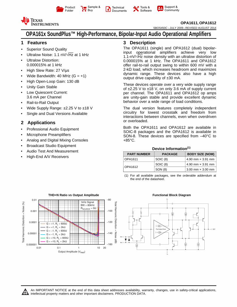
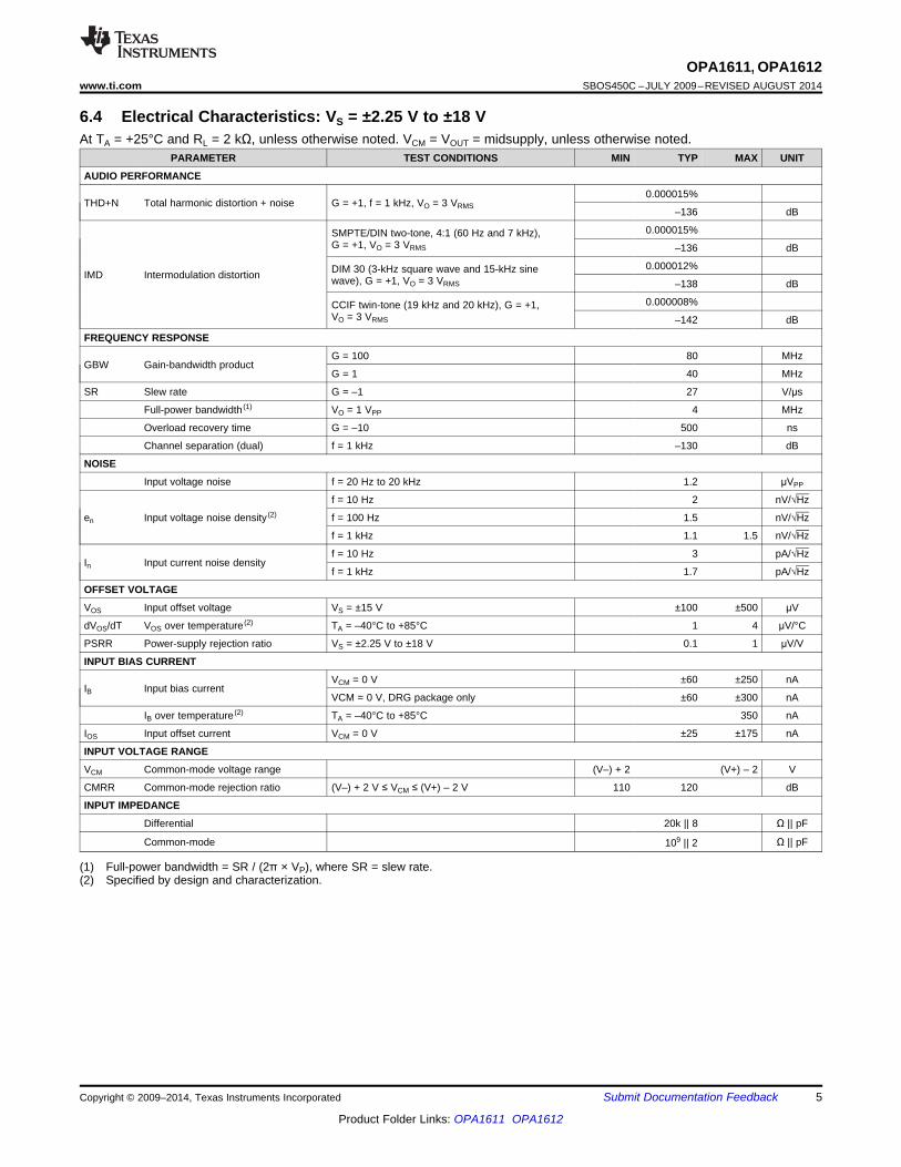
Pre-Output Driver OUT V- V+ IN- IN+ 0.01 0.001 0.0001 0.00001 0.000001 Total Harmonic Distortion + Noise (%) - - - - - 80 100 120 140 160 Total Harmonic Distortion + Noise (dB) 0.01 0.1 1 10 20 Output Amplitude (V ) RMS 1kHz Signal BW = 80kHz R = 0 SOURCE W G = +1, R = 600W L G = +1, R = 2k G = 1, R = 600 L L W - W G = 1, R = 2k G = +10, R = 600 G = +10, R = 2k - W W W L L L Product Folder Sample & Buy Technical Documents Tools & Software Support & Community OPA1611, OPA1612 SBOS450C – JULY 2009 – REVISED AUGUST 2014 OPA161x SoundPlus™ High-Performance, Bipolar-Input Audio Operational Amplifiers 1 Features 3 Description The OPA1611 (single) and OPA1612 (dual) bipolar- 1• Superior Sound Quality input operational amplifiers achieve very low • Ultralow Noise: 1.1 nV/√Hz at 1 kHz 1.1-nV/√Hz noise density with an ultralow distortion of • Ultralow Distortion: 0.000015% at 1 kHz. The OPA1611 and OPA1612 0.000015% at 1 kHz offer rail-to-rail output swing to within 600 mV with a 2-kΩ load, which increases headroom and maximizes • High Slew Rate: 27 V/μs dynamic range. These devices also have a high • Wide Bandwidth: 40 MHz (G = +1) output drive capability of ±30 mA. • High Open-Loop Gain: 130 dB These devices operate over a very wide supply range • Unity Gain Stable of ±2.25 V to ±18 V, on only 3.6 mA of supply current • Low Quiescent Current: per channel. The OPA1611 and OPA1612 op amps 3.6 mA per Channel are unity-gain stable and provide excellent dynamic behavior over a wide range of load conditions. • Rail-to-Rail Output • Wide Supply Range: ±2.25 V to ±18 V The dual version features completely independent circuitry for lowest crosstalk and freedom from • Single and Dual Versions Available interactions between channels, even when overdriven or overloaded. 2 Applications Both the OPA1611 and OPA1612 are available in • Professional Audio Equipment SOIC-8 packages and the OPA1612 is available in • Microphone Preamplifiers SON-8. These devices are specified from –40°C to • Analog and Digital Mixing Consoles +85°C. • Broadcast Studio Equipment Device Information (1) • Audio Test And Measurement PART NUMBER PACKAGE BODY SIZE (NOM) • High-End A/V Receivers OPA1611 SOIC (8) 4.90 mm × 3.91 mm SOIC (8) 4.90 mm × 3.91 mm OPA1612 SON (8) 3.00 mm × 3.00 mm (1) For all available packages, see the orderable addendum at the end of the datasheet. space space THD+N Ratio vs Output Amplitude Functional Block Diagram 1 An IMPORTANT NOTICE at the end of this data sheet addresses availability, warranty, changes, use in safety-critical applications, intellectual property matters and other important disclaimers. PRODUCTION DATA.
Transcript
Pre-Output Driver OUT
V-
V+
IN-
IN+
0.01
0.001
0.0001
0.00001
0.000001
Tota
l H
arm
on
ic D
isto
rtio
n +
No
ise
(%
)
-
-
-
-
-
80
100
120
140
160
Tota
l Ha
rmo
nic
Dis
tortio
n +
No
ise
(dB
)
0.01 0.1 1 10 20
Output Amplitude (V )RMS
1kHz Signal
BW = 80kHz
R = 0SOURCE W
G = +1, R = 600WL
G = +1, R = 2k
G = 1, R = 600L
L
W
- W
G = 1, R = 2k
G = +10, R = 600
G = +10, R = 2k
- W
W
W
L
L
L
Product
Folder
Sample &Buy
Technical
Documents
Tools &
Software
Support &Community
OPA1611, OPA1612SBOS450C –JULY 2009–REVISED AUGUST 2014
OPA161x SoundPlus™ High-Performance, Bipolar-Input Audio Operational Amplifiers1 Features 3 Description
The OPA1611 (single) and OPA1612 (dual) bipolar-1• Superior Sound Quality
input operational amplifiers achieve very low• Ultralow Noise: 1.1 nV/√Hz at 1 kHz 1.1-nV/√Hz noise density with an ultralow distortion of• Ultralow Distortion: 0.000015% at 1 kHz. The OPA1611 and OPA1612
0.000015% at 1 kHz offer rail-to-rail output swing to within 600 mV with a2-kΩ load, which increases headroom and maximizes• High Slew Rate: 27 V/μsdynamic range. These devices also have a high• Wide Bandwidth: 40 MHz (G = +1) output drive capability of ±30 mA.
• High Open-Loop Gain: 130 dBThese devices operate over a very wide supply range• Unity Gain Stable of ±2.25 V to ±18 V, on only 3.6 mA of supply current
• Low Quiescent Current: per channel. The OPA1611 and OPA1612 op amps3.6 mA per Channel are unity-gain stable and provide excellent dynamic
behavior over a wide range of load conditions.• Rail-to-Rail Output• Wide Supply Range: ±2.25 V to ±18 V The dual version features completely independent
circuitry for lowest crosstalk and freedom from• Single and Dual Versions Availableinteractions between channels, even when overdrivenor overloaded.2 ApplicationsBoth the OPA1611 and OPA1612 are available in• Professional Audio Equipment SOIC-8 packages and the OPA1612 is available in
• Microphone Preamplifiers SON-8. These devices are specified from –40°C to• Analog and Digital Mixing Consoles +85°C.• Broadcast Studio Equipment
Device Information(1)• Audio Test And Measurement
PART NUMBER PACKAGE BODY SIZE (NOM)• High-End A/V Receivers
OPA1611 SOIC (8) 4.90 mm × 3.91 mmSOIC (8) 4.90 mm × 3.91 mm
OPA1612SON (8) 3.00 mm × 3.00 mm
(1) For all available packages, see the orderable addendum atthe end of the datasheet.
space
spaceTHD+N Ratio vs Output Amplitude Functional Block Diagram
1
An IMPORTANT NOTICE at the end of this data sheet addresses availability, warranty, changes, use in safety-critical applications,intellectual property matters and other important disclaimers. PRODUCTION DATA.
11 Device and Documentation Support ................. 216.4 Electrical Characteristics: VS = ±2.25 V to ±18 V .... 511.1 Documentation Support ........................................ 216.5 Typical Characteristics .............................................. 711.2 Related Links ........................................................ 217 Detailed Description ............................................ 1211.3 Trademarks ........................................................... 217.1 Overview ................................................................. 1211.4 Electrostatic Discharge Caution............................ 217.2 Functional Block Diagram ....................................... 1211.5 Glossary ................................................................ 217.3 Feature Description................................................. 12
12 Mechanical, Packaging, and Orderable8 Application and Implementation ........................ 15 Information ........................................................... 21
4 Revision History
Changes from Revision B (July 2011) to Revision C Page
• Changed format to meet latest data sheet standards; added new sections, and moved existing sections........................... 1• Added SON-8 (DRG) package to data sheet ......................................................................................................................... 1• Changed SO to SOIC throughout document to match industry standard term...................................................................... 1• Added front-page curve .......................................................................................................................................................... 1• Added title to block diagram ................................................................................................................................................... 1• Deleted Package Information table; see package option addendum..................................................................................... 3
Changes from Revision A (August 2009) to Revision B Page
• Revised Features list items .................................................................................................................................................... 1• Updated front-page figure....................................................................................................................................................... 1• Added max specification for input voltage noise density at f = 1kHz .................................................................................... 5• Corrected typo in footnote 1 for Electrical Characteristics ..................................................................................................... 5• Revised Figure 4 .................................................................................................................................................................... 7• Updated Figure 7.................................................................................................................................................................... 7• Changed Figure 9 .................................................................................................................................................................. 7• Revised Figure 11 .................................................................................................................................................................. 7• Corrected typo in Figure 15.................................................................................................................................................... 8• Updated Figure 29................................................................................................................................................................ 12• Revised fourth paragraph of Electrincal Overstress section ................................................................................................ 13• Revised table in Figure 34.................................................................................................................................................... 17
OPA1611, OPA1612www.ti.com SBOS450C –JULY 2009–REVISED AUGUST 2014
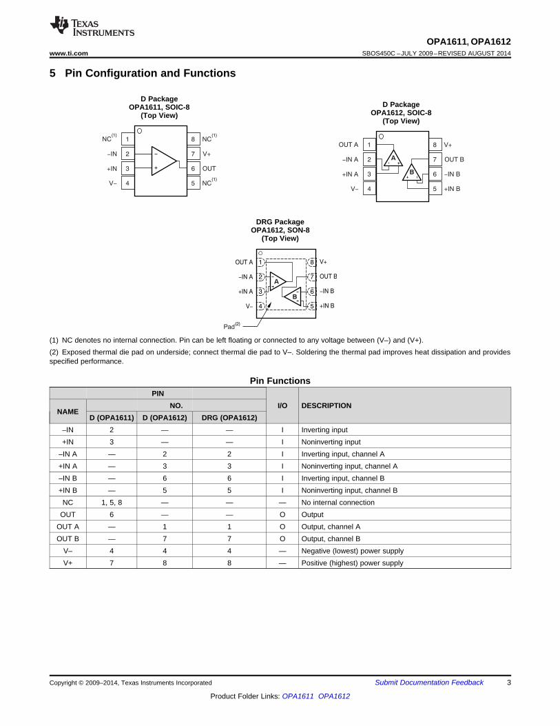
5 Pin Configuration and Functions
D PackageD PackageOPA1611, SOIC-8
OPA1612, SOIC-8(Top View)(Top View)
DRG PackageOPA1612, SON-8
(Top View)
(1) NC denotes no internal connection. Pin can be left floating or connected to any voltage between (V–) and (V+).(2) Exposed thermal die pad on underside; connect thermal die pad to V–. Soldering the thermal pad improves heat dissipation and providesspecified performance.
Pin FunctionsPIN
NO. I/O DESCRIPTIONNAME
D (OPA1611) D (OPA1612) DRG (OPA1612)–IN 2 — — I Inverting input+IN 3 — — I Noninverting input
–IN A — 2 2 I Inverting input, channel A+IN A — 3 3 I Noninverting input, channel A–IN B — 6 6 I Inverting input, channel B+IN B — 5 5 I Noninverting input, channel BNC 1, 5, 8 — — — No internal connection
OUT 6 — — O OutputOUT A — 1 1 O Output, channel AOUT B — 7 7 O Output, channel B
V– 4 4 4 — Negative (lowest) power supplyV+ 7 8 8 — Positive (highest) power supply
OPA1611, OPA1612SBOS450C –JULY 2009–REVISED AUGUST 2014 www.ti.com
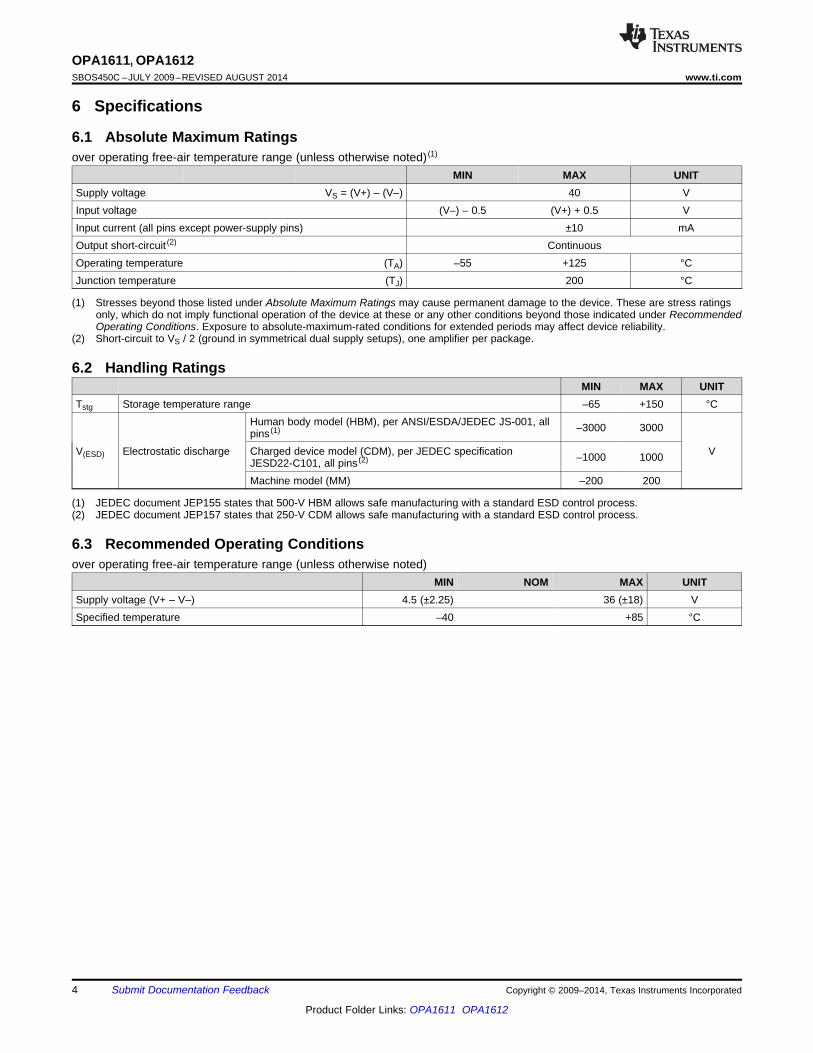
6 Specifications
6.1 Absolute Maximum Ratingsover operating free-air temperature range (unless otherwise noted) (1)
MIN MAX UNITSupply voltage VS = (V+) – (V–) 40 VInput voltage (V–) – 0.5 (V+) + 0.5 VInput current (all pins except power-supply pins) ±10 mAOutput short-circuit (2) ContinuousOperating temperature (TA) –55 +125 °CJunction temperature (TJ) 200 °C
(1) Stresses beyond those listed under Absolute Maximum Ratings may cause permanent damage to the device. These are stress ratingsonly, which do not imply functional operation of the device at these or any other conditions beyond those indicated under RecommendedOperating Conditions. Exposure to absolute-maximum-rated conditions for extended periods may affect device reliability.
(2) Short-circuit to VS / 2 (ground in symmetrical dual supply setups), one amplifier per package.
6.2 Handling RatingsMIN MAX UNIT
Tstg Storage temperature range –65 +150 °CHuman body model (HBM), per ANSI/ESDA/JEDEC JS-001, all –3000 3000pins (1)
V(ESD) Electrostatic discharge Charged device model (CDM), per JEDEC specification V–1000 1000JESD22-C101, all pins (2)
Machine model (MM) –200 200
(1) JEDEC document JEP155 states that 500-V HBM allows safe manufacturing with a standard ESD control process.(2) JEDEC document JEP157 states that 250-V CDM allows safe manufacturing with a standard ESD control process.
6.3 Recommended Operating Conditionsover operating free-air temperature range (unless otherwise noted)
MIN NOM MAX UNITSupply voltage (V+ – V–) 4.5 (±2.25) 36 (±18) VSpecified temperature –40 +85 °C
OPA1611, OPA1612SBOS450C –JULY 2009–REVISED AUGUST 2014 www.ti.com
Electrical Characteristics: VS = ±2.25 V to ±18 V (continued)At TA = +25°C and RL = 2 kΩ, unless otherwise noted. VCM = VOUT = midsupply, unless otherwise noted.
PARAMETER TEST CONDITIONS MIN TYP MAX UNIT
OPEN-LOOP GAIN
(V–) + 0.2 V ≤ VO ≤ (V+) – 0.2 V, RL = 10 kΩ 114 130 dBAOL Open-loop voltage gain
(V–) + 0.6 V ≤ VO ≤ (V+) – 0.6 V, RL = 2 kΩ 110 114 dB
OUTPUT
RL = 10 kΩ, AOL ≥ 114 dB (V–) + 0.2 (V+) – 0.2 VVOUT Voltage output
RL = 2 kΩ, AOL ≥ 110 dB (V–) + 0.6 (V+) – 0.6 V
IOUT Output current See Figure 27 mA
ZO Open-loop output impedance See Figure 28 Ω
+55 mAISC Short-circuit current
–62 mA
CLOAD Capacitive load drive See Typical Characteristics pF
POWER SUPPLY
VS Specified voltage ±2.25 ±18 V
IQ Quiescent current (per channel) IOUT = 0 A 3.6 4.5 mA
IQ over Temperature (3) TA = –40°C to +85°C 5.5 mA
OPA1611, OPA1612SBOS450C –JULY 2009–REVISED AUGUST 2014 www.ti.com
7 Detailed Description
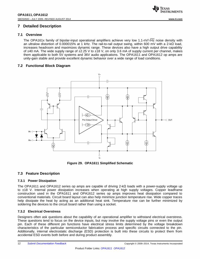
7.1 OverviewThe OPA161x family of bipolar-input operational amplifiers achieve very low 1.1-nV/√Hz noise density withan ultralow distortion of 0.000015% at 1 kHz. The rail-to-rail output swing, within 600 mV with a 2-kΩ load,increases headroom and maximizes dynamic range. These devices also have a high output drive capabilityof ±40 mA. The wide supply range of ±2.25 V to ±18 V, on only 3.6 mA of supply current per channel, makesthem applicable to both 5V systems and 36V audio applications. The OPA1611 and OPA1612 op amps areunity-gain stable and provide excellent dynamic behavior over a wide range of load conditions.
7.2 Functional Block Diagram
Figure 29. OPA1611 Simplified Schematic
7.3 Feature Description
7.3.1 Power DissipationThe OPA1611 and OPA1612 series op amps are capable of driving 2-kΩ loads with a power-supply voltage upto ±18 V. Internal power dissipation increases when operating at high supply voltages. Copper leadframeconstruction used in the OPA1611 and OPA1612 series op amps improves heat dissipation compared toconventional materials. Circuit board layout can also help minimize junction temperature rise. Wide copper traceshelp dissipate the heat by acting as an additional heat sink. Temperature rise can be further minimized bysoldering the devices to the circuit board rather than using a socket.
7.3.2 Electrical OverstressDesigners often ask questions about the capability of an operational amplifier to withstand electrical overstress.These questions tend to focus on the device inputs, but may involve the supply voltage pins or even the outputpin. Each of these different pin functions have electrical stress limits determined by the voltage breakdowncharacteristics of the particular semiconductor fabrication process and specific circuits connected to the pin.Additionally, internal electrostatic discharge (ESD) protection is built into these circuits to protect them fromaccidental ESD events both before and during product assembly.
OPA1611, OPA1612www.ti.com SBOS450C –JULY 2009–REVISED AUGUST 2014
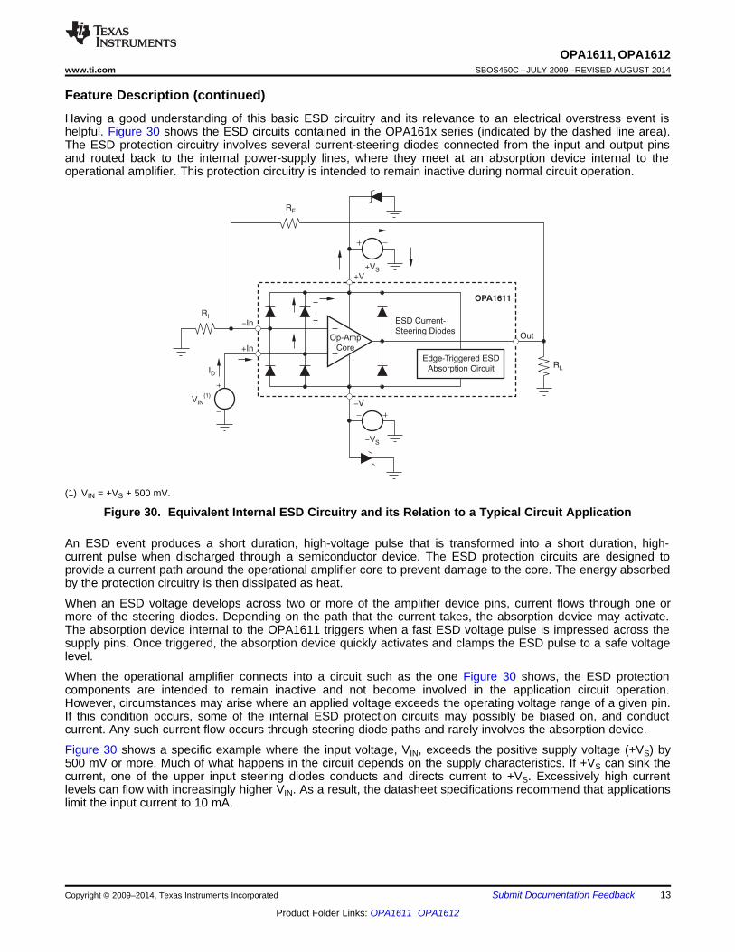
Feature Description (continued)Having a good understanding of this basic ESD circuitry and its relevance to an electrical overstress event ishelpful. Figure 30 shows the ESD circuits contained in the OPA161x series (indicated by the dashed line area).The ESD protection circuitry involves several current-steering diodes connected from the input and output pinsand routed back to the internal power-supply lines, where they meet at an absorption device internal to theoperational amplifier. This protection circuitry is intended to remain inactive during normal circuit operation.
(1) VIN = +VS + 500 mV.
Figure 30. Equivalent Internal ESD Circuitry and its Relation to a Typical Circuit Application
An ESD event produces a short duration, high-voltage pulse that is transformed into a short duration, high-current pulse when discharged through a semiconductor device. The ESD protection circuits are designed toprovide a current path around the operational amplifier core to prevent damage to the core. The energy absorbedby the protection circuitry is then dissipated as heat.
When an ESD voltage develops across two or more of the amplifier device pins, current flows through one ormore of the steering diodes. Depending on the path that the current takes, the absorption device may activate.The absorption device internal to the OPA1611 triggers when a fast ESD voltage pulse is impressed across thesupply pins. Once triggered, the absorption device quickly activates and clamps the ESD pulse to a safe voltagelevel.
When the operational amplifier connects into a circuit such as the one Figure 30 shows, the ESD protectioncomponents are intended to remain inactive and not become involved in the application circuit operation.However, circumstances may arise where an applied voltage exceeds the operating voltage range of a given pin.If this condition occurs, some of the internal ESD protection circuits may possibly be biased on, and conductcurrent. Any such current flow occurs through steering diode paths and rarely involves the absorption device.
Figure 30 shows a specific example where the input voltage, VIN, exceeds the positive supply voltage (+VS) by500 mV or more. Much of what happens in the circuit depends on the supply characteristics. If +VS can sink thecurrent, one of the upper input steering diodes conducts and directs current to +VS. Excessively high currentlevels can flow with increasingly higher VIN. As a result, the datasheet specifications recommend that applicationslimit the input current to 10 mA.
OPA1611, OPA1612SBOS450C –JULY 2009–REVISED AUGUST 2014 www.ti.com
Feature Description (continued)If the supply is not capable of sinking the current, VIN may begin sourcing current to the operational amplifier, andthen take over as the source of positive supply voltage. The danger in this case is that the voltage can rise tolevels that exceed the operational amplifier absolute maximum ratings. In extreme but rare cases, the absorptiondevice triggers on while +VS and –VS are applied. If this event happens, a direct current path is establishedbetween the +VS and –VS supplies. The power dissipation of the absorption device is quickly exceeded, and theextreme internal heating destroys the operational amplifier.
Another common question involves what happens to the amplifier if an input signal is applied to the input whilethe power supplies +VS or –VS are at 0 V. Again, the result depends on the supply characteristic while at 0 V, orat a level below the input signal amplitude. If the supplies appear as high impedance, then the operationalamplifier supply current may be supplied by the input source via the current steering diodes. This state is not anormal bias condition; the amplifier most likely does not operate normally. If the supplies are low impedance,then the current through the steering diodes can become quite high. The current level depends on the ability ofthe input source to deliver current, and any resistance in the input path.
If there is an uncertainty about the ability of the supply to absorb this current, external zener diodes may beadded to the supply pins; see Figure 30. The zener voltage must be selected such that the diode does not turnon during normal operation. However, the zener diode voltage must be low enough so that the zener diodeconducts if the supply pin begins to rise above the safe operating supply voltage level.
7.3.3 Operating VoltageThe OPA161x series op amps operate from ±2.25-V to ±18-V supplies while maintaining excellent performance.The OPA161x series can operate with as little as +4.5 V between the supplies and with up to +36 V between thesupplies. However, some applications do not require equal positive and negative output voltage swing. With theOPA161x series, power-supply voltages do not need to be equal. For example, the positive supply could be setto +25 V with the negative supply at –5 V.
In all cases, the common-mode voltage must be maintained within the specified range. In addition, keyparameters are assured over the specified temperature range of TA = –40°C to +85°C. Parameters that vary withoperating voltage or temperature are shown in the Typical Characteristics.
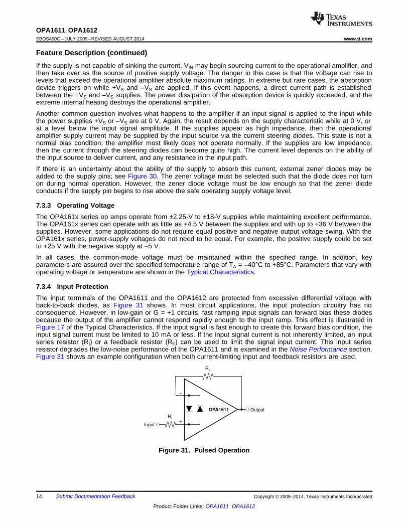
7.3.4 Input ProtectionThe input terminals of the OPA1611 and the OPA1612 are protected from excessive differential voltage withback-to-back diodes, as Figure 31 shows. In most circuit applications, the input protection circuitry has noconsequence. However, in low-gain or G = +1 circuits, fast ramping input signals can forward bias these diodesbecause the output of the amplifier cannot respond rapidly enough to the input ramp. This effect is illustrated inFigure 17 of the Typical Characteristics. If the input signal is fast enough to create this forward bias condition, theinput signal current must be limited to 10 mA or less. If the input signal current is not inherently limited, an inputseries resistor (RI) or a feedback resistor (RF) can be used to limit the signal input current. This input seriesresistor degrades the low-noise performance of the OPA1611 and is examined in the Noise Performance section.Figure 31 shows an example configuration when both current-limiting input and feedback resistors are used.
OPA1611, OPA1612www.ti.com SBOS450C –JULY 2009–REVISED AUGUST 2014
8 Application and Implementation
8.1 Application InformationThe OPA1611 and OPA1612 are unity-gain stable, precision op amps with very low noise; these devices are alsofree from output phase reversal. Applications with noisy or high-impedance power supplies require decouplingcapacitors close to the device power-supply pins. In most cases, 0.1-μF capacitors are adequate.
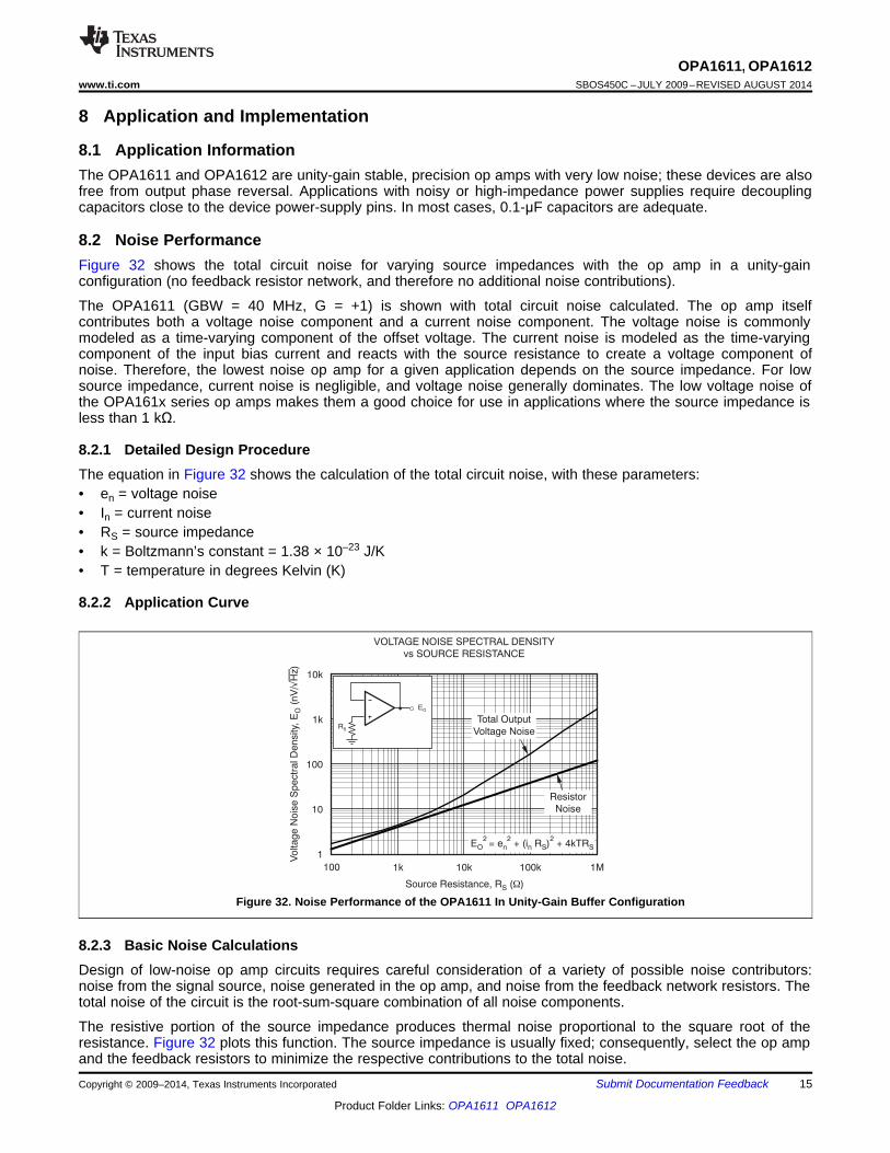
8.2 Noise PerformanceFigure 32 shows the total circuit noise for varying source impedances with the op amp in a unity-gainconfiguration (no feedback resistor network, and therefore no additional noise contributions).
The OPA1611 (GBW = 40 MHz, G = +1) is shown with total circuit noise calculated. The op amp itselfcontributes both a voltage noise component and a current noise component. The voltage noise is commonlymodeled as a time-varying component of the offset voltage. The current noise is modeled as the time-varyingcomponent of the input bias current and reacts with the source resistance to create a voltage component ofnoise. Therefore, the lowest noise op amp for a given application depends on the source impedance. For lowsource impedance, current noise is negligible, and voltage noise generally dominates. The low voltage noise ofthe OPA161x series op amps makes them a good choice for use in applications where the source impedance isless than 1 kΩ.
8.2.1 Detailed Design ProcedureThe equation in Figure 32 shows the calculation of the total circuit noise, with these parameters:• en = voltage noise• In = current noise• RS = source impedance• k = Boltzmann’s constant = 1.38 × 10⁻²³ J/K• T = temperature in degrees Kelvin (K)
8.2.2 Application Curve
Figure 32. Noise Performance of the OPA1611 In Unity-Gain Buffer Configuration
8.2.3 Basic Noise CalculationsDesign of low-noise op amp circuits requires careful consideration of a variety of possible noise contributors:noise from the signal source, noise generated in the op amp, and noise from the feedback network resistors. Thetotal noise of the circuit is the root-sum-square combination of all noise components.
The resistive portion of the source impedance produces thermal noise proportional to the square root of theresistance. Figure 32 plots this function. The source impedance is usually fixed; consequently, select the op ampand the feedback resistors to minimize the respective contributions to the total noise.
OPA1611, OPA1612SBOS450C –JULY 2009–REVISED AUGUST 2014 www.ti.com
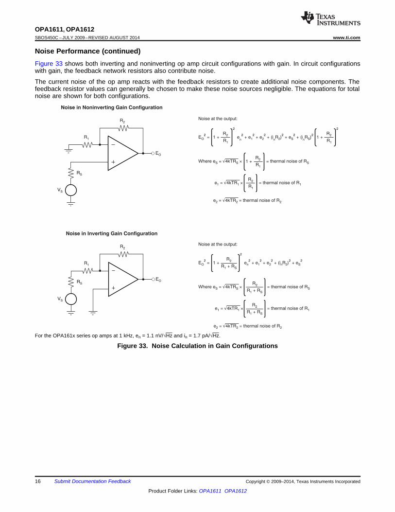
Noise Performance (continued)Figure 33 shows both inverting and noninverting op amp circuit configurations with gain. In circuit configurationswith gain, the feedback network resistors also contribute noise.
The current noise of the op amp reacts with the feedback resistors to create additional noise components. Thefeedback resistor values can generally be chosen to make these noise sources negligible. The equations for totalnoise are shown for both configurations.
For the OPA161x series op amps at 1 kHz, en = 1.1 nV/√Hz and in = 1.7 pA/√Hz.
Figure 33. Noise Calculation in Gain Configurations
OPA1611, OPA1612www.ti.com SBOS450C –JULY 2009–REVISED AUGUST 2014
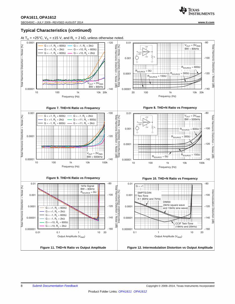
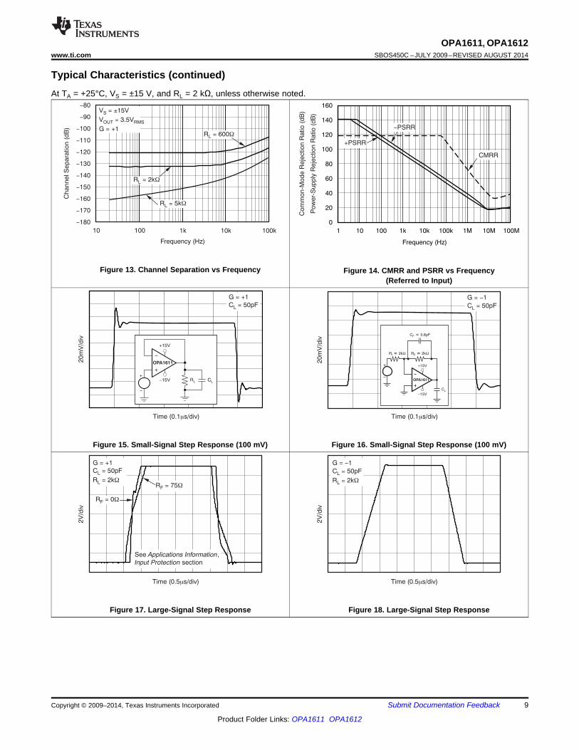
8.3 Total Harmonic Distortion MeasurementsThe OPA161x series op amps have excellent distortion characteristics. THD + noise is below 0.00008% (G = +1,VO = 3 VRMS, BW = 80 kHz) throughout the audio frequency range, 20 Hz to 20 kHz, with a 2-kΩ load (seeFigure 7 for characteristic performance).
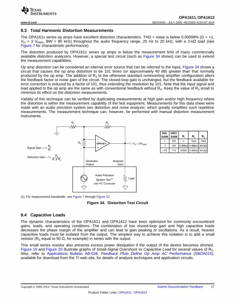
The distortion produced by OPA1611 series op amps is below the measurement limit of many commerciallyavailable distortion analyzers. However, a special test circuit (such as Figure 34 shows) can be used to extendthe measurement capabilities.
Op amp distortion can be considered an internal error source that can be referred to the input. Figure 34 shows acircuit that causes the op amp distortion to be 101 times (or approximately 40 dB) greater than that normallyproduced by the op amp. The addition of R3 to the otherwise standard noninverting amplifier configuration altersthe feedback factor or noise gain of the circuit. The closed-loop gain is unchanged, but the feedback available forerror correction is reduced by a factor of 101, thus extending the resolution by 101. Note that the input signal andload applied to the op amp are the same as with conventional feedback without R3. Keep the value of R3 small tominimize its effect on the distortion measurements.
Validity of this technique can be verified by duplicating measurements at high gain and/or high frequency wherethe distortion is within the measurement capability of the test equipment. Measurements for this data sheet weremade with an audio precision system two distortion and noise analyzer, which greatly simplifies such repetitivemeasurements. The measurement technique can, however, be performed with manual distortion measurementinstruments.
(1) For measurement bandwidth, see Figure 7 through Figure 12.
Figure 34. Distortion Test Circuit
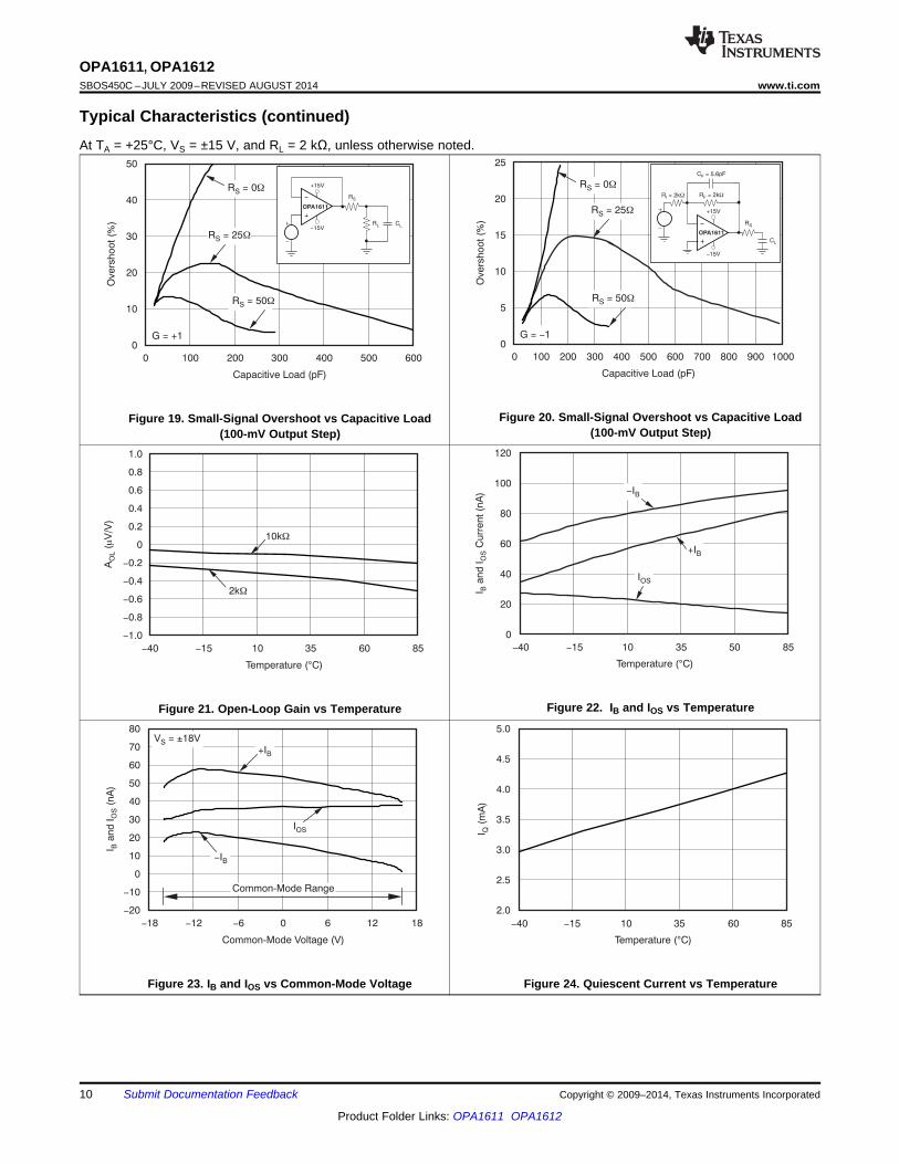
8.4 Capacitive LoadsThe dynamic characteristics of the OPA1611 and OPA1612 have been optimized for commonly encounteredgains, loads, and operating conditions. The combination of low closed-loop gain and high capacitive loadsdecreases the phase margin of the amplifier and can lead to gain peaking or oscillations. As a result, heaviercapacitive loads must be isolated from the output. The simplest way to achieve this isolation is to add a smallresistor (RS equal to 50 Ω, for example) in series with the output.
This small series resistor also prevents excess power dissipation if the output of the device becomes shorted.Figure 19 and Figure 20 illustrate graphs of Small-Signal Overshoot vs Capacitive Load for several values of RS.Also, refer to Applications Bulletin AB-028, Feedback Plots Define Op Amp AC Performance (SBOA015),available for download from the TI web site, for details of analysis techniques and application circuits.
OPA1611, OPA1612SBOS450C –JULY 2009–REVISED AUGUST 2014 www.ti.com
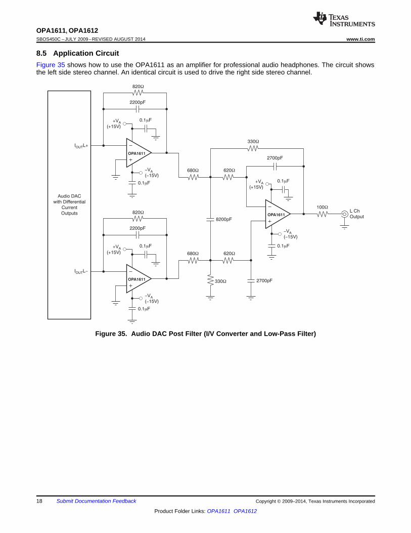
8.5 Application CircuitFigure 35 shows how to use the OPA1611 as an amplifier for professional audio headphones. The circuit showsthe left side stereo channel. An identical circuit is used to drive the right side stereo channel.
Figure 35. Audio DAC Post Filter (I/V Converter and Low-Pass Filter)
OPA1611, OPA1612www.ti.com SBOS450C –JULY 2009–REVISED AUGUST 2014
9 Power-Supply RecommendationsThe OPA161x is specified for operation from 4.5 V to 36 V (±2.25 V to ±18 V); many specifications apply from–40°C to +85°C. Parameters that can exhibit significant variance with regard to operating voltage or temperatureare presented in the Typical Characteristics section.
CAUTIONSupply voltages larger than 40 V can permanently damage the device; see theAbsolute Maximum Ratings.
Place 0.1-μF bypass capacitors close to the power-supply pins to reduce errors coupling in from noisy or high-impedance power supplies. For more detailed information on bypass capacitor placement, refer to the TypicalCharacteristics section.
dual-supplyoperation Ground (GND) plane on another layer
VOUT
VIN
GND
Run the input tracesas far away fromthe supply lines
as possible
Use low-ESR, ceramic bypass capacitor
RF
RG
RIN
Place components close to device and to each other to reduce
parasitic errors
+VINVOUT
RIN
RG
RF
(Schematic Representation)
OPA1611, OPA1612SBOS450C –JULY 2009–REVISED AUGUST 2014 www.ti.com
10 Layout
10.1 Layout GuidelinesFor best operational performance of the device, use good printed circuit board (PCB) layout practices, including:• Noise can propagate into analog circuitry through the power pins of the circuit as a whole and the op amp
itself. Bypass capacitors are used to reduce the coupled noise by providing low-impedance power sourceslocal to the analog circuitry.– Connect low-ESR, 0.1-µF ceramic bypass capacitors between each supply pin and ground, placed as
close to the device as possible. A single bypass capacitor from V+ to ground is applicable for single-supply applications.
• Separate grounding for analog and digital portions of the circuitry is one of the simplest and most-effectivemethods of noise suppression. One or more layers on multilayer PCBs are usually devoted to ground planes.A ground plane helps distribute heat and reduces EMI noise pickup. Make sure to physically separate digitaland analog grounds while paying attention to the flow of the ground current. For more detailed information,refer to the application report Circuit Board Layout Techniques (SLOA089).
• In order to reduce parasitic coupling, run the input traces as far away from the supply or output traces aspossible. If these traces cannot be keep them separate, crossing the sensitive trace perpendicular asopposed to in parallel with the noisy trace is the preferred method.
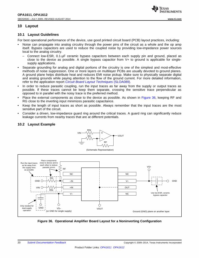
• Place the external components as close to the device as possible. As shown in Figure 36, keeping RF andRG close to the inverting input minimizes parasitic capacitance.
• Keep the length of input traces as short as possible. Always remember that the input traces are the mostsensitive part of the circuit.
• Consider a driven, low-impedance guard ring around the critical traces. A guard ring can significantly reduceleakage currents from nearby traces that are at different potentials.
10.2 Layout Example
Figure 36. Operational Amplifier Board Layout for a Noninverting Configuration
OPA1611, OPA1612www.ti.com SBOS450C –JULY 2009–REVISED AUGUST 2014
11 Device and Documentation Support
11.1 Documentation Support
11.1.1 Related DocumentationFor related documentation see the following:• Feedback Plots Define Op Amp AC Performance , SBOA015• Circuit Board Layout Techniques, SLOA089
11.2 Related LinksThe table below lists quick access links. Categories include technical documents, support and communityresources, tools and software, and quick access to sample or buy.
Table 1. Related LinksTECHNICAL TOOLS & SUPPORT &PARTS PRODUCT FOLDER SAMPLE & BUY DOCUMENTS SOFTWARE COMMUNITY
OPA1611 Click here Click here Click here Click here Click hereOPA1612 Click here Click here Click here Click here Click here
11.3 TrademarksSoundPlus is a trademark of Texas Instruments, Inc.All other trademarks are the property of their respective owners.
11.4 Electrostatic Discharge CautionThese devices have limited built-in ESD protection. The leads should be shorted together or the device placed in conductive foamduring storage or handling to prevent electrostatic damage to the MOS gates.
11.5 GlossarySLYZ022 — TI Glossary.
This glossary lists and explains terms, acronyms, and definitions.
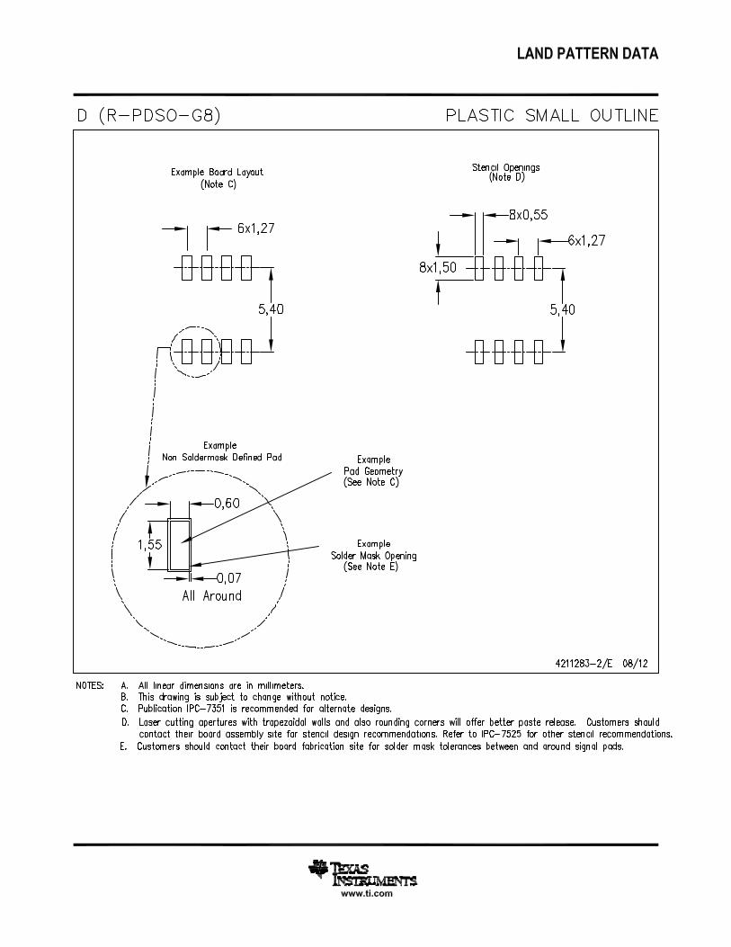
12 Mechanical, Packaging, and Orderable InformationThe following pages include mechanical, packaging, and orderable information. This information is the mostcurrent data available for the designated devices. This data is subject to change without notice and revision ofthis document. For browser-based versions of this data sheet, refer to the left-hand navigation.
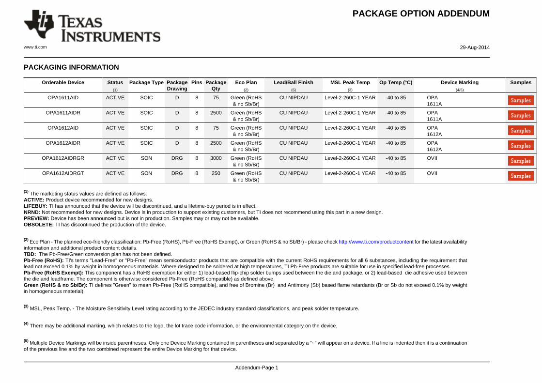
OPA1611AID ACTIVE SOIC D 8 75 Green (RoHS& no Sb/Br)
CU NIPDAU Level-2-260C-1 YEAR -40 to 85 OPA1611A
OPA1611AIDR ACTIVE SOIC D 8 2500 Green (RoHS& no Sb/Br)
CU NIPDAU Level-2-260C-1 YEAR -40 to 85 OPA1611A
OPA1612AID ACTIVE SOIC D 8 75 Green (RoHS& no Sb/Br)
CU NIPDAU Level-2-260C-1 YEAR -40 to 85 OPA1612A
OPA1612AIDR ACTIVE SOIC D 8 2500 Green (RoHS& no Sb/Br)
CU NIPDAU Level-2-260C-1 YEAR -40 to 85 OPA1612A
OPA1612AIDRGR ACTIVE SON DRG 8 3000 Green (RoHS& no Sb/Br)
CU NIPDAU Level-2-260C-1 YEAR -40 to 85 OVII
OPA1612AIDRGT ACTIVE SON DRG 8 250 Green (RoHS& no Sb/Br)
CU NIPDAU Level-2-260C-1 YEAR -40 to 85 OVII
(1) The marketing status values are defined as follows:ACTIVE: Product device recommended for new designs.LIFEBUY: TI has announced that the device will be discontinued, and a lifetime-buy period is in effect.NRND: Not recommended for new designs. Device is in production to support existing customers, but TI does not recommend using this part in a new design.PREVIEW: Device has been announced but is not in production. Samples may or may not be available.OBSOLETE: TI has discontinued the production of the device.
(2) Eco Plan - The planned eco-friendly classification: Pb-Free (RoHS), Pb-Free (RoHS Exempt), or Green (RoHS & no Sb/Br) - please check http://www.ti.com/productcontent for the latest availabilityinformation and additional product content details.TBD: The Pb-Free/Green conversion plan has not been defined.Pb-Free (RoHS): TI's terms "Lead-Free" or "Pb-Free" mean semiconductor products that are compatible with the current RoHS requirements for all 6 substances, including the requirement thatlead not exceed 0.1% by weight in homogeneous materials. Where designed to be soldered at high temperatures, TI Pb-Free products are suitable for use in specified lead-free processes.Pb-Free (RoHS Exempt): This component has a RoHS exemption for either 1) lead-based flip-chip solder bumps used between the die and package, or 2) lead-based die adhesive used betweenthe die and leadframe. The component is otherwise considered Pb-Free (RoHS compatible) as defined above.Green (RoHS & no Sb/Br): TI defines "Green" to mean Pb-Free (RoHS compatible), and free of Bromine (Br) and Antimony (Sb) based flame retardants (Br or Sb do not exceed 0.1% by weightin homogeneous material)
(3) MSL, Peak Temp. - The Moisture Sensitivity Level rating according to the JEDEC industry standard classifications, and peak solder temperature.
(4) There may be additional marking, which relates to the logo, the lot trace code information, or the environmental category on the device.
(5) Multiple Device Markings will be inside parentheses. Only one Device Marking contained in parentheses and separated by a "~" will appear on a device. If a line is indented then it is a continuationof the previous line and the two combined represent the entire Device Marking for that device.
(6) Lead/Ball Finish - Orderable Devices may have multiple material finish options. Finish options are separated by a vertical ruled line. Lead/Ball Finish values may wrap to two lines if the finishvalue exceeds the maximum column width.
Important Information and Disclaimer:The information provided on this page represents TI's knowledge and belief as of the date that it is provided. TI bases its knowledge and belief on informationprovided by third parties, and makes no representation or warranty as to the accuracy of such information. Efforts are underway to better integrate information from third parties. TI has taken andcontinues to take reasonable steps to provide representative and accurate information but may not have conducted destructive testing or chemical analysis on incoming materials and chemicals.TI and TI suppliers consider certain information to be proprietary, and thus CAS numbers and other limited information may not be available for release.
In no event shall TI's liability arising out of such information exceed the total purchase price of the TI part(s) at issue in this document sold by TI to Customer on an annual basis.
IMPORTANT NOTICETexas Instruments Incorporated and its subsidiaries (TI) reserve the right to make corrections, enhancements, improvements and otherchanges to its semiconductor products and services per JESD46, latest issue, and to discontinue any product or service per JESD48, latestissue. Buyers should obtain the latest relevant information before placing orders and should verify that such information is current andcomplete. All semiconductor products (also referred to herein as “components”) are sold subject to TI’s terms and conditions of salesupplied at the time of order acknowledgment.TI warrants performance of its components to the specifications applicable at the time of sale, in accordance with the warranty in TI’s termsand conditions of sale of semiconductor products. Testing and other quality control techniques are used to the extent TI deems necessaryto support this warranty. Except where mandated by applicable law, testing of all parameters of each component is not necessarilyperformed.TI assumes no liability for applications assistance or the design of Buyers’ products. Buyers are responsible for their products andapplications using TI components. To minimize the risks associated with Buyers’ products and applications, Buyers should provideadequate design and operating safeguards.TI does not warrant or represent that any license, either express or implied, is granted under any patent right, copyright, mask work right, orother intellectual property right relating to any combination, machine, or process in which TI components or services are used. Informationpublished by TI regarding third-party products or services does not constitute a license to use such products or services or a warranty orendorsement thereof. Use of such information may require a license from a third party under the patents or other intellectual property of thethird party, or a license from TI under the patents or other intellectual property of TI.Reproduction of significant portions of TI information in TI data books or data sheets is permissible only if reproduction is without alterationand is accompanied by all associated warranties, conditions, limitations, and notices. TI is not responsible or liable for such altereddocumentation. Information of third parties may be subject to additional restrictions.Resale of TI components or services with statements different from or beyond the parameters stated by TI for that component or servicevoids all express and any implied warranties for the associated TI component or service and is an unfair and deceptive business practice.TI is not responsible or liable for any such statements.Buyer acknowledges and agrees that it is solely responsible for compliance with all legal, regulatory and safety-related requirementsconcerning its products, and any use of TI components in its applications, notwithstanding any applications-related information or supportthat may be provided by TI. Buyer represents and agrees that it has all the necessary expertise to create and implement safeguards whichanticipate dangerous consequences of failures, monitor failures and their consequences, lessen the likelihood of failures that might causeharm and take appropriate remedial actions. Buyer will fully indemnify TI and its representatives against any damages arising out of the useof any TI components in safety-critical applications.In some cases, TI components may be promoted specifically to facilitate safety-related applications. With such components, TI’s goal is tohelp enable customers to design and create their own end-product solutions that meet applicable functional safety standards andrequirements. Nonetheless, such components are subject to these terms.No TI components are authorized for use in FDA Class III (or similar life-critical medical equipment) unless authorized officers of the partieshave executed a special agreement specifically governing such use.Only those TI components which TI has specifically designated as military grade or “enhanced plastic” are designed and intended for use inmilitary/aerospace applications or environments. Buyer acknowledges and agrees that any military or aerospace use of TI componentswhich have not been so designated is solely at the Buyer's risk, and that Buyer is solely responsible for compliance with all legal andregulatory requirements in connection with such use.TI has specifically designated certain components as meeting ISO/TS16949 requirements, mainly for automotive use. In any case of use ofnon-designated products, TI will not be responsible for any failure to meet ISO/TS16949.Products ApplicationsAudio www.ti.com/audio Automotive and Transportation www.ti.com/automotiveAmplifiers amplifier.ti.com Communications and Telecom www.ti.com/communicationsData Converters dataconverter.ti.com Computers and Peripherals www.ti.com/computersDLP® Products www.dlp.com Consumer Electronics www.ti.com/consumer-appsDSP dsp.ti.com Energy and Lighting www.ti.com/energyClocks and Timers www.ti.com/clocks Industrial www.ti.com/industrialInterface interface.ti.com Medical www.ti.com/medicalLogic logic.ti.com Security www.ti.com/securityPower Mgmt power.ti.com Space, Avionics and Defense www.ti.com/space-avionics-defenseMicrocontrollers microcontroller.ti.com Video and Imaging www.ti.com/videoRFID www.ti-rfid.comOMAP Applications Processors www.ti.com/omap TI E2E Community e2e.ti.comWireless Connectivity www.ti.com/wirelessconnectivity