1. INTRODUCTIONElectromagnetic wave scattering by surface grooves and slitshas been treated numerically by various methods includingthe finite element method [1,2], the finite-difference time-domain [3–6], the method of moments [7,8], and the Fouriermodal method, also called rigorous coupled-wave analysis ormode-matching method [9–15]. This paper describes a source-model technique (SMT) [16] solution for this class of pro-blems. The SMT is a mesh-free, integral-equation method thatis simple to implement and applicable to arbitrary geometricalshapes. It is closely related to a number of other methods: theGeneralized Multipole Technique [17], the Method of AuxiliarySources [18,19], the Method of Fictitious Sources [20,21], andthe Method of Fundamental Solutions [22]. Although the SMThas been extensively applied to a wide range of scattering pro-blems [23–30], it has not been applied to analyze scattering bysurface grooves and slits.
This paper presents an SMT-based approach to solve scat-tering by surface grooves and slits. A similar SMT-based ap-proach has recently proven its usefulness in the context ofdefects in photonic crystals [29]. The idea is to treat thegrooves and slits as perturbations in the structure and usea superposition of the solution of the unperturbed problem,and local corrections in the groove/slit region. In this manner,the solution is obtained in a much faster way than solving theoriginal problem. It also facilitates fast analysis of a largenumber of different perturbations for a given (unperturbed)geometry.
The proposed solution is applied to problems of groovesand slits in otherwise planar or periodic, perfectly conductingmetal as well as dielectric surfaces. In the planar surfacescase, the solution of the unperturbed problem is knownanalytically. In the periodic surfaces case, the solution of theunperturbed problem is obtained numerically using anefficient SMT solution that employs periodic sources [24].Grooves and slits of various shapes, both smooth ones as wellas ones with edges, empty or filled with dielectric material,
can be analyzed. In the context of groove problems, the focusis on the scattered field, while in the context of slit problems,the focus is mainly on the field transmitted by the slit. Thislatter problem has received a lot of attention recently, parti-cularly in studies of enhanced transmission through subwave-length slits [4–6,12–14,31,32].
This paper is organized as follows. The SMT is described inSection 2. The formulation for the two representative casesbeing analyzed, namely, that of a dielectric-filled rectangulargroove in a planar perfectly conducting metal surface and thatof a slit in corrugated perfectly conducting metal screen, isgiven in Section 3. Numerical results for these two casesare presented in Section 4. Finally, a summary and conclu-sions are given in Section 5.
2. SOURCE-MODEL TECHNIQUEIn the SMT, the scattered fields in each of the homogenousregions of the problem space are approximated by a superpo-sition of fields of fictitious current sources located outsidethat region. Each fictitious current source is assumed to radi-ate in an unbounded region with the same material propertiesas the region that produces the fields. In this way, the approx-imate field in each region automatically satisfies Maxwell’sequations. What we do next, is adjust the amplitudes of thesefictitious sources for the continuity condition (in some mini-mum error sense) at a discrete set of matching points (MPs)across the interfaces between the various regions. A sche-matic example of a two-dimensional scattering problem invol-ving two different dielectric regions that are assumed to beinfinite in the z direction is shown in Fig. 1. If the polarizationof the incident wave is TE (i.e., the electric field is in the zdirection, transverse to the plane of incidence), filamentaryelectric sources are used. If the polarization of the incidentwave is TM (i.e., the magnetic field is in the z direction, trans-verse to the plane of incidence), filamentary magnetic sourcesare used. Naturally, the electromagnetic field produced by
502 J. Opt. Soc. Am. A / Vol. 28, No. 4 / April 2011 K. Trotskovsky and Y. Leviatan
each of these filamentary sources, when radiating in a homo-geneous unbounded medium, can be derived analytically.
3. FORMULATIONAs mentioned in Section 1, the proposed solution method canbe applied to both scattering by a groove and transmissionthrough slit problems. For each type of problem, the unper-turbed surface can be planar (for which the solution is knownanalytically) or periodic (for which the solution can be foundnumerically). In addition, both empty or dielectric-filledgrooves and slits can be treated. Clearly, we will not presentthe formulation for each of the possible cases; rather, we willconcentrate on two representative cases, that of a dielectric-filled rectangular groove in a planar perfectly conductingmetal surface and that of a slit in a corrugated perfectly con-ducting metal screen.
A. Dielectric-Filled Rectangular Grooves in a PlanarPerfectly Conducting Metal SurfaceThe geometry of a dielectric-filled rectangular groove in a pla-nar perfectly conducting metal (PEC) surface is shown inFig. 2. In this case, two sets of fictitious sources are used.The first set, denoted by SpI , is assumed to produce the per-turbation to the fields in region I caused by the dielectric-filledgroove. The second set, denoted by SpII, is assumed to producethe total fields in the dielectric-filled groove in region II.
The total electromagnetic fields in regions I and II are
EI ¼ Einc þ Es0I þ Es;p
I ðSpI Þ; HI ¼ Hinc þHs0I þHs;p
I ðSpI Þ;EII ¼ Es;p
II ðSpIIÞ; HII ¼ Hs;pII ðSp
IIÞ:ð1Þ
Here, the subscript stands for the relevant region where thefields are evaluated; Einc;Hinc denotes the incident electricand magnetic fields; Es0
I ;Hs0I denotes the scattered electric
and magnetic fields in region I in the case of the auxiliary(unperturbed) problem; Es;p
I ðSpI Þ;Hs;pI ðSpI Þ denotes the pertur-
bation to the electric and magnetic fields in region I, as pro-duced by the sources SpI ; and EII ¼ Es;p
II ðSpIIÞ, HII ¼ Hs;pII ðSpIIÞ
denotes the total electric and magnetic fields in region II,as produced by the sources SpII. The boundary and continuityconditions are
n̂×ðEinc þ Es0I þ Es;p
I ðSpI ÞÞ ¼ 0 on A;
n̂ × Es;pII ðSpIIÞ ¼ 0 on B;
n̂ × ðEinc þ Es0I þ Es;p
I ðSpI ÞÞ ¼ n̂ × Es;pII ðSp
IIÞ on C;
n̂ × ðHinc þHs0I þHs;p
I ðSpI ÞÞ ¼ n̂ ×Hs;pII ðSpIIÞ on C: ð2Þ
In the SMT solution, these conditions are imposed, eitherstrictly or in a least squares error sense, at a finite set ofMPs. Clearly, one should ensure that these conditions are alsosatisfied to a specified degree of accuracy, both between theMPs on A, B, and C, as well as outside the MP region on A. Toquantify this accuracy, we define the boundary conditionerrors ΔEbc on A and B, and the continuity condition errorsΔEcc and ΔHcc on C as
ΔEbcj n̂×ðEinc þ Es0
I þ Es;pI ðSpI ÞÞj
jEincj on A;
ΔEbc ¼j n̂×Es;p
II ðSpIIÞjjEincj on B;
ΔEcc ¼j n̂×ðEinc þ Es0
I þ Es;pI ðSpI Þ − Es;p
II ðSpIIÞÞj����12 n̂ × ðEinc þ Es0
I þ Es;pI ðSpI Þ þ Es;p
II ðSpIIÞÞ����
on C;
ΔHcc ¼j n̂×ðHinc þHs0
I þHs;pI ðSpI Þ �Hs;p
II ðSpIIÞÞj����12 n̂ × ðHinc þHs0
I þHs;pI ðSpI Þ þHs;p
II ðSpIIÞÞ����
on C:
ð3Þ
Fig. 1. Scheme of a two-dimensional scattering problem involving two dielectric regions. (a) Original problem. (b) Equivalence for region I, withthe scattered filed being produced by fictitious filamentary sources located in region II. (c) Equivalence for region II, with the total field beingproduced by fictitious filamentary sources located in region I.
Fig. 2. (Color online) Scattering by a dielectric-filled rectangulargroove in a planar perfectly conducting metal surface. (a) Geometryof the original (perturbed) problem. (b) Geometry of the auxiliary (un-perturbed) problem of scattering by a planar perfectly conductingmetal surface. (c) Sources producing the fields that simulate the per-turbation to the fields in region I, caused by the dielectric-filledgrooves and the corresponding MPs. (d) Sources producing the fieldsthat simulate the total fields in region II, and the corresponding MPs.Here, A designates the interface between region I and the PEC, B des-ignates the interface between region II and the PEC, and C designatesthe interface between regions I and region II.
K. Trotskovsky and Y. Leviatan Vol. 28, No. 4 / April 2011 / J. Opt. Soc. Am. A 503
When choosing the number of sources and MPs and theirlocations, the goal is to attain the required degree of accuracy,using as few sources and MPs as possible. In the problem un-der consideration, there are two characteristically differenttypes of regions: planar boundary surfaces and edges.
Near planar boundary surfaces, the sources are placed withspacing ds;s between them, and at a constant distance ds;mp
from the surface. Numerical studies have shown that the ratiods;mp=ds;s should be of the order of 1–2. Clearly, if ds;mp ≪ ds;s,the error between the MPs might be large, whereas ifds;mp ≫ ds;s, the field produced by the sources will no longerbe able to accurately span rapid field variations on the sur-face. The spacing between the sources located far away fromthe region of the groove, is chosen to be ds;s ¼ λ=3. This isbecause three sources per wavelength are sufficient for span-ning fields scattered by a planar infinite surface illuminated bya plane wave. However, in the vicinity of the groove, morethan three sources per wavelength are naturally required.Thus, the density of the sources is gradually increased aswe approach the region of the groove, reaching a densityas high as 50 per wavelength near the groove edges.
Another noteworthy issue is the extent of the region withinthe sources and MPs are placed. Clearly, this extent will de-termine the region where the error is guaranteed to be small.In regards to the error outside this region, because the effectof the groove on the scattered fields is localized, this error canbe made small enough to conform to a desired level by gra-dually increasing that region.
A different approach to the choice of source and MP loca-tions should be exercised near edges, where the field may ex-hibit singular behavior. A scheme of the layout of the sourcesand MPs near an edge is shown in Fig. 3. In a similar way to[25], three structural arrangements of sources are used:straight-line sources that are facing the planar surfaces (likethe ones described earlier); tapered-curve sources that are lo-cated on a curve and gradually approaching the intersectingplanar surfaces forming the edge; and edge sources that arelocated on straight lines stretching between the innermosttapered-curve sources and the edge, with the distance be-tween them decreasing as a geometric series.
When choosing the number of MPs in the SMT, one gener-ally has two options. The first is choosing an equal number ofMPs and sources. In this case, the boundary/continuity condi-tion error is zero at the MPs. Clearly, the fidelity of the solu-tion is affected by the extent of the error between the MPs.The second, which is computationally more costly but oftenpreferable, is choosing a larger number of MPs than sources,
and finding the source’s values by a Least Squares method.With this choice of more MPs than sources, there will be nopoints with zero boundary/continuity condition error, but thepeak error throughout will be lower than with the choice ofequal number of MPs and sources. However, pursuing a leastsquares solution in cases involving edges, when the excitationis TM, is not a good option. In this case, the singularity of thetangential electric field near the edge, leads inevitably to alarge boundary condition error near the edge. Now, if therewere more MPs than sources, this large error would not beconfined to the region near the edge, but rather averaged tothe whole surface, and render the solution inaccurate. Hence,while both aforementioned options are suitable when the ex-citation of the rectangular groove is TE, if the excitation is TM,it is necessary to use an equal number of MPs and sources.
Another point to be considered is the number of sources(and the corresponding number of MPs) needed for spanningthe fields in dielectric regions compared to that in vacuum.The number of sources in the case of dielectric regions is de-termined by the wavelength in the dielectric and would ordi-narily be larger by ε1=2r than that in the case of vacuum (εrbeing the dielectric constant of the region). As to the choiceof the sources (and corresponding MPs) near the interface be-tween two different dielectric media, this is naturally dictatedby the wavelength in the denser material. For example, in thecase of Fig. 2, there will be more sources, not only in the set SpIIspanning the fields in the dielectric region, but also in the setSpI located near the groove interface and spanning the fields inregion I, just above the groove.
B. Slit in a Corrugated Perfectly ConductingMetal ScreenThe geometry of a slit in a corrugated perfectly conductingmetal screen excited by a plane wave is shown in Fig. 4(a).The pertinent auxiliary (unperturbed) problem of a periodicperfectly conducting metal surface excited by a plane waveis shown in Fig. 4(b). First, we tackle the periodic problem.An efficient SMT solution of this problem, for the case ofTE polarization, was presented by Boag and Leviatan [24].We adopted this solution, and in a straightforward manner,also extended it to encompass the case of TM polarization.The solution idea is to use periodic current sources S0I , ex-press their fields as a sum of an infinite series of Floquetmodes, and reduce the problem to a consideration of the fieldswithin a unit cell of the periodic structure [see Fig. 4(c)].Moreover, to render the convergence of the series of Floquetmodes representing the fields of the periodic sources muchfaster, strips of currents, with smooth current distribution,rather than filamentary currents, were used. After solvingthe unperturbed problem for the complex amplitudes of thesources simulating the unperturbed fields in region I, we pro-ceed to the perturbed problem. To simulate the actual fields inregion I, we used, alongside the already determined periodicsources S0I , a set of filamentary current sources SpI , of yet to bedetermined complex amplitudes [see Fig. 4(d)]. The set ofsources SpI , is assumed to produce the perturbation to theknown periodic fields in region I caused by the slit. To simu-late the fields in region II, another set of filamentary currentsources SpII, of yet to be determined complex amplitudes isused [see Fig. 4(e)]. The set of sources SpII is assumed to pro-duce the total fields in region II.Fig. 3. (Color online) Sources and MPs near an edge.
504 J. Opt. Soc. Am. A / Vol. 28, No. 4 / April 2011 K. Trotskovsky and Y. Leviatan
The total electromagnetic fields in regions I and II are
EI ¼ Einc þ Es0I þ Es;p
I ðSpI Þ; HI ¼ Hinc þHs0
I þHs;pI ðSpI Þ;
EII ¼ Es;pII ðSpIIÞ; HII ¼ Hs;p
II ðSpIIÞ:ð4Þ
Here, the subscript stands for the relevant region where thefield are evaluated; Einc;Hinc denotes the incident electric andmagnetic fields; Es0
I ;Hs0I denotes the scattered electric and
magnetic fields in region I in the case of the auxiliary (unper-turbed) periodic problem; Es;p
I ðSpI Þ;Hs;pI ðSpI Þ denotes the
perturbation to the electric and magnetic fields in region I,as produced by the sources SpI ; and EII ¼ Es;p
II ðSpIIÞ;HII ¼Hs;p
II ðSpIIÞ denotes the total electric and magnetic field in regionII, as produced by the sources SpII. The boundary and continu-ity conditions are
n̂×ðEinc þ Es0I þ Es;p
I ðSpI ÞÞ ¼ 0 on A;
n̂ × Es;pII ðSpIIÞ ¼ 0 on B;
n̂ × ðEinc þ Es0I þ Es;p
I ðSpI ÞÞ ¼ n̂ × Es;pII ðSp
IIÞ on C;
n̂ × ðHinc þHs0I þHs;p
I ðSpI ÞÞ ¼ n̂ ×Hs;pII ðSpIIÞ on C: ð5Þ
As discussed in Subsection 3.A, these conditions are im-posed in the SMT solution, either strictly or in a least squareserror sense at a finite set of MPs. The accuracy is measured interms of boundary and continuity condition error defined inan analogous manner to (3). In regards to the choice of thenumber of sources and MPs, as well as their locations, we
can proceed along the same lines of the SMT solution tothe groove problem described in Subsection 3.A. Handlingedges can also be done in much the same way as in the groovecase. Finally, regarding the extent of the sources and MPs, thisshould be increased, like in the groove case, until the error ismade small enough to conform to a desired level of accuracy.
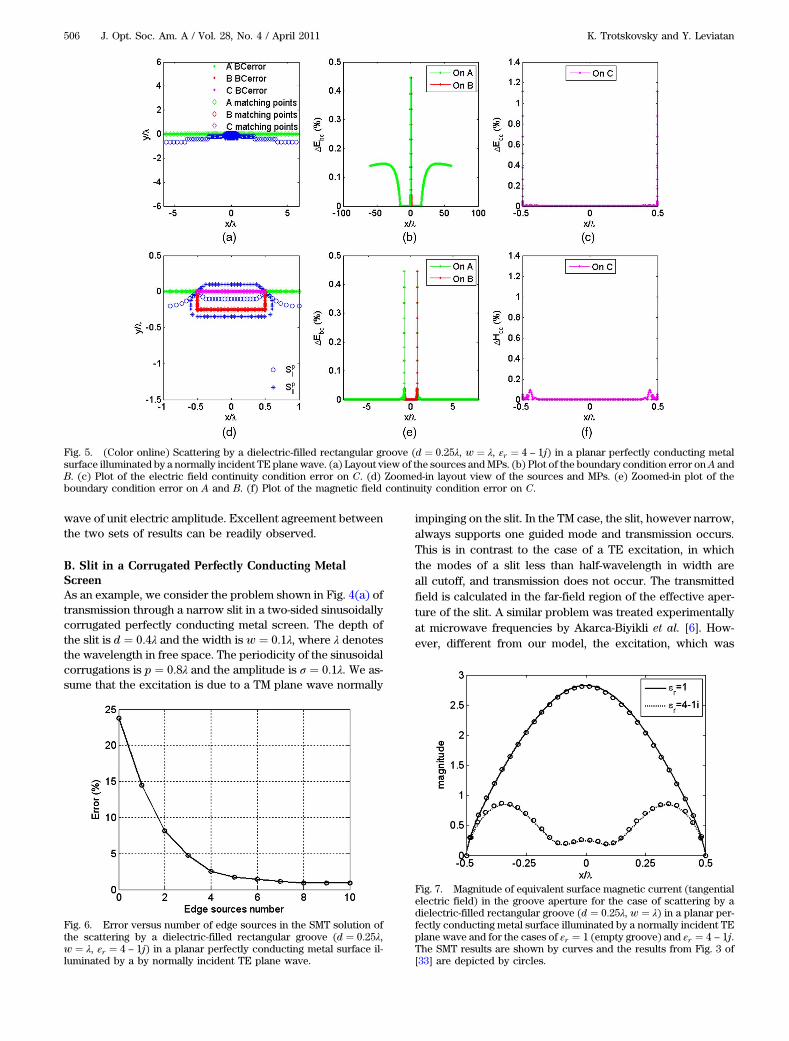
4. NUMERICAL RESULTSA. Dielectric-Filled Rectangular Grooves in a PlanarPerfectly Conducting Metal SurfaceAs an example, we consider the problem of scattering by adielectric-filled groove that was solved by Jin and Volakis[33] using a combined FEM and integral method. The depthof the groove is d ¼ 0:25λ and the width is w ¼ λ, where λ de-notes the wavelength in free space. The groove is filled withmaterial of relative dielectric constant εr ¼ 4 − 1j. The excita-tion is due to an incident TE plane wave (TM in the notation of[33]) normally impinging on the groove.
In the SMT solution, the sources and MPs were placed inthe region jxj ≤ 15w ¼ 15λ. The extent of the region of thesources and MPs was sufficient to render the error outsidethe region as satisfactorily small. The layout of the sourcesand MPs used in the solution is shown in Fig. 5, along withplots of the boundary condition error on A and B and the con-tinuity condition errors of C. To obtain these results, we usedan equal number of sources and MPs and distributed them inaccordance with the guidelines suggested in Subsection 3.A. Ifds;s ¼ 0:1λ and ds;mp ¼ 2ds;s ¼ 0:2λ, we had 217 sources be-sides the edge sources. We also took an additional sevensources per straight line, near each of the two edges. Becausethere are four straight lines associated with each edge, two forthe sources belonged to the set SpI and two for the sourcesbelonged to the set SpII. There are additional 8 × 7 ¼ 56 edgesources, and the total number of sources we used amountedto 273. The boundary and continuity condition errors in theregion jxj ≤ 15w ¼ 15λ are tested at a finer set of points, con-sisting of 10 points between each pair of adjacent MPs. Theboundary and condition error in the region jxj ≥ 15w ¼ 15λis tested at a set with similar density. As seen in Fig. 5(b),the error throughout the region jxj ≤ 15w ¼ 15λ is very small,except near the two edges. The error in the region jxj ≥ 15w ¼15λ is a bit larger, but still less than 0.15%.
To check the convergence of the solution with the changein the number of sources, we kept the 217 sources besides theedge sources intact and gradually increased the number ofedge sources. The decrease in the maximal boundary/continu-ity condition error of the electric and magnetic fields on A, B,and C, when the number of sources per straight line increases,is shown in Fig. 6. Notice again that increasing the indicatednumber of sources per straight line by one, implies increasingthe total number of sources by eight. This is because there arefour straight lines, two for the sources belonging to the set SpIand two for the sources belonging to the set SpII, associatedwith each one of the two edges.
A comparison between the results obtained by the pro-posed SMT solution and the results obtained by Jin and Vola-kis [33] for both the case of εr ¼ 1 (empty groove) and thecase of εr ¼ 4 − 1j is shown in Fig. 7. The plots depict the mag-nitude of the equivalent surface magnetic current (tangentialelectric field) in the groove aperture for an incident plane
Fig. 4. (Color online) Transmission through a slit in a perfectlyconducting corrugated metal screen. (a) Geometry of the original(perturbed) problem. (b) Geometry of the auxiliary (unperturbed)problem of scattering by a periodically corrugated perfectly conduct-ing metal surface. (c) Sources producing the fields that simulate thefields in region I in the unperturbed case, and the corresponding MPs.(d) Sources producing the fields that simulate the perturbation to thefields in region I caused by the slit, and the corresponding MPs.(e) Sources producing the fields that simulate the actual fields in re-gion II, and the corresponding MPs. Here, A designates the interfacebetween region I and the PEC, B designates the interface betweenregion II and the PEC, and C designates the interface between regionI and region II.
K. Trotskovsky and Y. Leviatan Vol. 28, No. 4 / April 2011 / J. Opt. Soc. Am. A 505
wave of unit electric amplitude. Excellent agreement betweenthe two sets of results can be readily observed.
B. Slit in a Corrugated Perfectly Conducting MetalScreenAs an example, we consider the problem shown in Fig. 4(a) oftransmission through a narrow slit in a two-sided sinusoidallycorrugated perfectly conducting metal screen. The depth ofthe slit is d ¼ 0:4λ and the width is w ¼ 0:1λ, where λ denotesthe wavelength in free space. The periodicity of the sinusoidalcorrugations is p ¼ 0:8λ and the amplitude is σ ¼ 0:1λ. We as-sume that the excitation is due to a TM plane wave normally
impinging on the slit. In the TM case, the slit, however narrow,always supports one guided mode and transmission occurs.This is in contrast to the case of a TE excitation, in whichthe modes of a slit less than half-wavelength in width areall cutoff, and transmission does not occur. The transmittedfield is calculated in the far-field region of the effective aper-ture of the slit. A similar problem was treated experimentallyat microwave frequencies by Akarca-Biyikli et al. [6]. How-ever, different from our model, the excitation, which was
Fig. 5. (Color online) Scattering by a dielectric-filled rectangular groove (d ¼ 0:25λ, w ¼ λ, εr ¼ 4 − 1j) in a planar perfectly conducting metalsurface illuminated by a normally incident TE plane wave. (a) Layout view of the sources andMPs. (b) Plot of the boundary condition error onA andB. (c) Plot of the electric field continuity condition error on C. (d) Zoomed-in layout view of the sources and MPs. (e) Zoomed-in plot of theboundary condition error on A and B. (f) Plot of the magnetic field continuity condition error on C.
Fig. 6. Error versus number of edge sources in the SMT solution ofthe scattering by a dielectric-filled rectangular groove (d ¼ 0:25λ,w ¼ λ, εr ¼ 4 − 1j) in a planar perfectly conducting metal surface il-luminated by a by normally incident TE plane wave.
Fig. 7. Magnitude of equivalent surface magnetic current (tangentialelectric field) in the groove aperture for the case of scattering by adielectric-filled rectangular groove (d ¼ 0:25λ, w ¼ λ) in a planar per-fectly conducting metal surface illuminated by a normally incident TEplane wave and for the cases of εr ¼ 1 (empty groove) and εr ¼ 4 − 1j.The SMT results are shown by curves and the results from Fig. 3 of[33] are depicted by circles.
506 J. Opt. Soc. Am. A / Vol. 28, No. 4 / April 2011 K. Trotskovsky and Y. Leviatan
due to a horn antenna located at some finite distance from thefront side of the corrugated screen, was not a plane wave.Also, in their case, the transmitted field, that was measuredby another horn antenna located at some finite distance fromthe back side of the corrugated screen, was not in the far-fieldregion of the effective aperture of the slit.
The layout of the sources and MPs used in the solution isshown in Fig. 8, along with plots of the boundary conditionerror on A and B and the continuity condition errors on C.To obtain these results, we used an equal number of sourcesand MPs, and distributed them in accord with the guidelinessuggested in Subsection 3.B. The total number of sourcesamounts to 309 for region I and 338 for region II. As explainedearlier in the text, choosing an equal number of sources andMPs is essential here, because the excitation is TM. In a waysimilar to the groove case, the boundary and continuity con-dition errors are tested at a finer set of points both betweenthe considered MPs as well as way beyond the outermost MPs.Further examination of Fig. 8 reveals that the boundary/continuity condition errors are satisfactorily low, except, asexpected, near the edges at ðx; yÞ ¼ ð�w=2; 0Þ and ðx; yÞ ¼ð�w=2;−dÞ, where the electric field is singular. The regionthat the sources and MPs were placed, stretched out over10 periods of corrugations (10p ¼ 8λ) from each side ofthe slit.
Like in the case of the rectangular groove in a planar sur-face considered earlier, the extent of the region within thesources and MPs are placed, readily determine the regionwhere the error is guaranteed to be small. Hence, in our solu-tion, we increased the extent of this region and checkedthat the boundary conditions are indeed fulfilled to a better
accuracy and that the results for the transmitted fields haveconverged. Regarding the boundary condition error outsideand away from the source and MPs region, this error maynot always diminish like it did in the previously analyzedgroove case. This is because a slit surrounded by perfectlyconducting periodic corrugations may give rise to a surfacewave that propagates to infinity without being attenuated.The existence of such surface waves is manifested by a con-stant boundary condition error. This constant boundary con-dition error is proportional to the amplitude of the excitedsurface wave, but it has a small, if any, effect on the calculatedvalues of the transmitted fields. The results shown here are forthe smallest region of sources and MPs that still yielded accu-rate transmitted field.
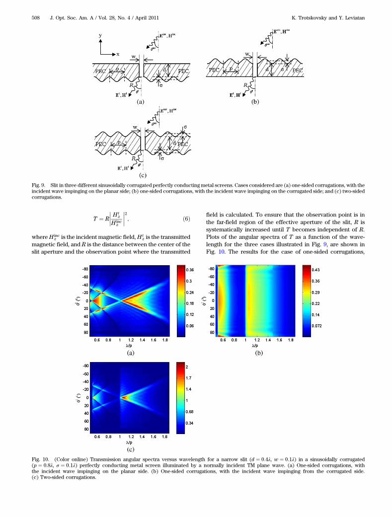
To demonstrate the beaming phenomenon, we solved theslit problem for three different sinusoidally corrugated per-fectly conducting metal screens. The three cases consideredare shown in Fig. 9. The geometrical dimensions in the threecases are identical, being as in the case of Fig. 8, d ¼ 0:4λ,w ¼ 0:1λ, p ¼ 0:8λ, and σ ¼ 0:1λ. In the case of the one-sidedcorrugations, with the incident wave impinging on the planarside [shown in Fig. 9(a)], the unperturbed surface is planar,and the solution of the unperturbed problem is known analy-tically. In the case of the one-sided corrugations, with the in-cident wave impinging on the corrugated side [Fig. 9(b)], andin the case of the two-sided corrugations [Fig. 9(c)], the un-perturbed surface is periodic, and the solution of the unper-turbed problem is obtained numerically using an efficient SMTsolution that employs periodic sources [24].
To quantify the transmission through the aperture, wedefine a transmission coefficient T given by
Fig. 8. (Color online) Transmission through a narrow slit (d ¼ 0:4λ, w ¼ 0:1λ) in a two-sided sinusoidally corrugated perfectly conducting metalscreen (p ¼ 0:8λ, σ ¼ 0:1λ) illuminated by a normally incident TM plane wave. (a) Layout view of the sources and MPs. (b) Plot of the boundarycondition error on A and B. (c) Plot of the electric field continuity condition error on C. (d) Zoomed-in layout view of the sources and MPs.(e) Zoomed-in plot of the boundary condition error on A and B.(f) Plot of the magnetic field continuity condition error on C.
K. Trotskovsky and Y. Leviatan Vol. 28, No. 4 / April 2011 / J. Opt. Soc. Am. A 507
T ¼ R
����
Htz
H incz
����
2; ð6Þ
whereH incz is the incident magnetic field,Ht
z is the transmittedmagnetic field, and R is the distance between the center of theslit aperture and the observation point where the transmitted
field is calculated. To ensure that the observation point is inthe far-field region of the effective aperture of the slit, R issystematically increased until T becomes independent of R.Plots of the angular spectra of T as a function of the wave-length for the three cases illustrated in Fig. 9, are shown inFig. 10. The results for the case of one-sided corrugations,
Fig. 9. Slit in three different sinusoidally corrugated perfectly conductingmetal screens. Cases considered are (a) one-sided corrugations, with theincident wave impinging on the planar side; (b) one-sided corrugations, with the incident wave impinging on the corrugated side; and (c) two-sidedcorrugations.
Fig. 10. (Color online) Transmission angular spectra versus wavelength for a narrow slit (d ¼ 0:4λ, w ¼ 0:1λ) in a sinusoidally corrugated(p ¼ 0:8λ, σ ¼ 0:1λ) perfectly conducting metal screen illuminated by a normally incident TM plane wave. (a) One-sided corrugations, withthe incident wave impinging on the planar side. (b) One-sided corrugations, with the incident wave impinging from the corrugated side.(c) Two-sided corrugations.
508 J. Opt. Soc. Am. A / Vol. 28, No. 4 / April 2011 K. Trotskovsky and Y. Leviatan
with the incident wave impinging on the planar side[Fig. 10(a)], demonstrate that enhanced transmission indeedoccurs at angles θtm satisfying
sin θtm ¼ mλp
� kSPk0
; ð7Þ
where m ∈ N, k0 is the wave number of free space, and kSP ¼kSPðk0Þ is the wave number of the spoof surface plasmon ex-cited on the transmission side, which, to a good approxima-tion, is given by kSP ≅ k0. Similar results, albeit for rectangularand not sinusoidal corrugations, were obtained in [13,14]. Inthe case of one-sided corrugation, with the incident wave im-pinging on the corrugated side [Fig. 10(b)] as expected, nospoof surface plasmon is excited on the transmission side,thus no angular dependence of the transmission exists. Butbecause the incidence is normal for wavelengths satisfying
0 ¼ mλp
� kSPk0
; ð8Þ
a spoof surface plasmon is excited on the input side, leading tohigher power concentration from the input side into the slit,and thus to increased transmission. For two-sided corruga-tions [Fig. 10(c)], we see similar beaming angles behaviorto Fig. 10(a) (similar geometrical dimensions of the outputcorrugations) with additional enhancement due to the inputcorrugations.
5. SUMMARYWe have presented a computational approach, based on theSMT, to analyze scattering by groove and slit perturbationsin otherwise planar or periodic perfectly conducting metalas well as dielectric surfaces. The formulations for two repre-sentative scattering problems, namely, that of a dielectric-filled rectangular groove in a planar perfectly conductingmetal surface and that of a slit in a corrugated perfectly con-ducting metal screen, have been outlined. A source layoutsuitable for expanding the fields near the edges has been pro-posed. The solutions were validated both by checking intern-ally that the required boundary and continuity conditions arefulfilled to a satisfactory degree, and by comparing the resultsobtained with published experimental and numerical data.The proposed computational approach can be readily appliedto study the characteristics of the scattering by different de-fects in planar and periodic surfaces, which may occur, forexample, during the fabrication process. It can also be readilyapplied to an analysis of enhancement and directivity in thecontext of transmission through subwavelength slits of var-ious shapes in planar and periodic surfaces, a problem whichhas received a lot of attention recently.
REFERENCES1. B. Alavikia and O. M. Ramahi, “Finite-element solution of the
problem of scattering from cavities in metallic screens usingthe surface integral equation as a boundary constraint,” J.Opt. Soc. Am. A 26, 1915–1925 (2009).
2. O. T. Janssen, H. P. Urbach, and G. W. ’t Hooft, “On the phase ofplasmons excited by slits in a metal film,” Opt. Express 14,11823–11832 (2006).
3. Y. Xie, A. Zakharian, J. Moloney, and M. Mansuripur, “Trans-mission of light through slit apertures in metallic films,” Opt.Express 12, 6106 6121 (2004).
4. D. A. Thomas and H. P. Hughes, “Enhanced optical transmissionthrough a subwavelength 1D aperture,” Solid State Commun.129, 519–524 (2004).
5. L. Yu, D. Lin, Y. Chen, Y. Chang, K. Huang, J. Liaw, J. Yeh, J. Liu,C. Yeh, and C. Lee, “Physical origin of directional beamingemitted from a subwavelength slit,” Phys. Rev. B 71, 41405(2005).
6. S. S. Akarca-Biyikli, I. Bulu, and E. Ozbay, “Resonant excitationof surface plasmons in one-dimensional metallic grating struc-tures at microwave frequencies,” J. Opt. A Pure Appl. Opt. 7,S159–S164 (2005).
7. Y. Shifman and Y. Leviatan, “Scattering by a groove in a conduct-ing plane-a PO-MoM hybrid formulation and wavelet analysis,”IEEE Trans. Antennas Propag. 49, 1807–1811 (2001).
8. Y. Tretiakov and G. W. Pan, “Coifman wavelets in electromag-netic wave scattering by a groove in conducting plane,” Prog.Electromagn. Res. PIER. 45, 1–20 (2004).
9. J. Bravo-Abad, L. Martín-Moreno, and F. García-Vidal, “Trans-mission properties of a single metallic slit: from the subwave-length regime to the geometrical-optics limit,” Phys. Rev. E69 (2004).
10. Y. Takakura, “Optical resonance in a narrow slit in a thickmetallic screen,” Phys. Rev. Lett. 86, 5601–5603 (2001).
11. S. H. Kang, H. J. Eom, and T. J. Park, “TM scattering from a slit ina thick conducting screen: revisited,” IEEE Trans. MicrowaveTheory Tech. 41, 895–899 (1993).
12. F. García-Vidal, L. Martín-Moreno, and J. B. Pendry, “Surfaceswith holes in them: new plasmonic metamaterials,” J. Opt. APure Appl. Opt. 7, S97–S101 (2005).
13. Y. Liu, H. Shi, C. Wang, C. Du, and X. Luo, “Multiple directionalbeaming effect of metallic subwavelength slit surrounded byperiodically corrugated grooves,” Opt. Express 16, 4487–4493(2008).
14. L. Martín-Moreno, F. García-Vidal, H. J. Lezec, A. Degiron, andT. W. Ebbesen, “Theory of highly directional emission from asingle subwavelength aperture surrounded by surface corruga-tions,” Phys. Rev. Lett. 90, 167401 (2003).
15. M. A. Basha, S. K. Chaudhuri, S. Safavi-Naeini, and H. J. Eom,“Rigorous formulation for electromagnetic plane-wave scatter-ing from a general-shaped groove in a perfectly conductingplane: reply to comment,” J. Opt. Soc. Am. A 25, 1167–1168(2008).
16. Y. Leviatan and A. Boag, “Generalized formulations for electro-magnetic scattering from perfectly conducting and homoge-neous material bodies-theory and numerical solution,” IEEETrans. Antennas Propag. 36, 1722–1734 (1988).
17. C. Hafner, The Generalized Multipole Technique for Computa-
tional Electromagnetics (Artech, 1990).18. D. I. Kaklamani and H. T. Anastassiu, “Aspects of the method of
19. O. M. Bucci, G. D’Elia, and M. Santojanni, “Non-redundantimplementation of method of auxiliary sources for smooth 2Dgeometries,” Electron. Lett. 41, 1203–1205 (2005).
20. G. Tayeb and S. Enoch, “Combined fictitious-sources-scattering-matrix method,” J. Opt. Soc. Am. A 21, 1417–1423(2004).
21. D. Maystre, M. Saillard, and G. Tayeb, “Special methods of wavediffraction,” in Scattering: Scattering and Inverse Scattering in
Pure and Applied Science, E. R. Pike and P. C. Sabatier, eds.(Academic, 2001), Chap. 1.5.6.
22. G. Fairweather and A. Karageorghis, “The method of fundamen-tal solutions for elliptic boundary value problems,” Adv. Com-put. Math. 9, 69–95 (1998).
23. Y. Leviatan, A. Boag, and A. Boag, “Analysis of TE scatteringfrom dielectric cylinders using a multifilament magnetic currentmodel,” IEEE Trans. Antennas Propag. 36, 1026–1031 (1988).
24. A. Boag and Y. Leviatan, “Analysis of two-dimensional electro-magnetic scattering from nonplanar periodic surfaces using astrip current model,” IEEE Trans. Antennas Propag. 37,1437–1446 (1989).
25. S. Eisler and Y. Leviatan, “Analysis of electromagnetic scatteringfrom metallic and penetrable cylinders with edges using a multi-filament current model,” IEE Proc. H: Microwaves, AntennasPropag. 136, 431–438 (1989).
K. Trotskovsky and Y. Leviatan Vol. 28, No. 4 / April 2011 / J. Opt. Soc. Am. A 509
26. E. Erez and Y. Leviatan, “Current-model analysis of electromag-netic scattering from objects containing a variety of length-scales,” J. Opt. Soc. Am. A 11, 1500–1504 (1994).
27. Y. Leviatan, Z. Baharav, and E. Heyman, “Analysis of electro-magnetic scattering using arrays of fictitious sources,” IEEETrans. Antennas Propag. 43, 1091–1098 (1995).
28. A. Ludwig and Y. Leviatan, “Analysis of band-gap character-istics of two-dimensional periodic structures using the source-model technique,” J. Opt. Soc. Am. A 20, 1553–1562(2003).
29. A. Ludwig and Y. Leviatan, “Analysis of arbitrary defects inphotonic crystals by use of the source-model technique,” J.Opt. Soc. Am. A 21, 1334–1343 (2004).
30. A. Ludwig and Y. Leviatan, “Time-domain analysis of band-gapcharacteristics of two-dimensional periodic structures by use ofa source-model technique,” J. Opt. Soc. Am. A 25, 437–451(2008).
31. T. Thio, K. M. Pellerin, R. A. Linke, H. J. Lezec, andT. W. Ebbesen, “Enhanced light transmission through a singlesubwavelength aperture,” Opt. Lett. 26, 1972–1974 (2001).
32. H. J. Lezec, A. Degiron, E. Devaux, R. A. Linke, L. Martin-Moreno, F. J. Garcia-Vidal, and T. W. Ebbesen, “Beaming lightfrom a subwavelength aperture,” Science 297, 820–822 (2002).
33. J. Jin and J. L. Volakis, “TM scattering by an inhomogeneouslyfilled aperture in a thick conducting plane,” IEE Proc. H: Micro-waves, Antennas Propag. 137, 153–159 (1990).
510 J. Opt. Soc. Am. A / Vol. 28, No. 4 / April 2011 K. Trotskovsky and Y. Leviatan