48
www.macom.com Product Selection Guide Space & High-Reliability

www.macom.com
Product Selection Guide
Space & High-Reliability
Space_HiRel brochure_051316_final_Space_HiRel brochure_040316 5/22/16 1:44 PM Page 1

MACOM continues to build upon our legacy of providing
high-reliability semiconductor products to the Aerospace and
Defense industry by adding to our product portfolio and capabilities
with high-reliability semiconductors for the military, defense,
satellite and aerospace industries. Products include rectifiers,
switching diodes, Zener diodes, temperature compensated Zeners,
current regulators, transient voltage suppressors, silicon controlled
rectifiers, small signal and power transistors, JANHC and JANKC
qualified chips.
MACOM also offers customer-specific design capabilities.
Environmental screening is available on most products. Additionally,
we have expertise in replacement designs for obsolete or discontinued
products. Our applications engineering support team is responsive,
flexible, innovative, and ready to help you with your next project.
Additional product information can be found on our website at
www.macom.com. Contact our worldwide sales offices, authorized
representatives, and industry-leading distributors to request samples,
test boards, and application support. All contacts are listed on our
website at: http://www.macom.com/contact
Partners from RF to Light
Copyright © 2016, MACOM Technology Solutions Inc. All Rights Reserved. This Product Selection Guide is provided by MACOM as a service to its customers andmay be used for informational purposes only by the customer. MACOM assumes no responsibility for errors or omissions in the Guide. MACOM and its affiliatesreserve the right to change any specification, designs, models and other information contained herein without notice. MACOM makes no commitment to update the information and shall have no responsibility whatsoever for conflicts, incompatibilities, or other difficulties arising from future changes to its documentation, products,specifications and product descriptions.
The products listed herein are subject to US Export Controls set forth by the Arms Export Control Act and the Export Administration Act.
Space_HiRel brochure_051316_final_Space_HiRel brochure_040316 5/22/16 1:44 PM Page 2
Contents
1
Space & Hi-Rel.......................4-15> General Purpose Gain Block Hybrid Amplifiers > Low Noise Hybrid Amplifiers> Mixers> Switches: SPDT> Power Dividers > Rad Hard Transistor Chips> Zener Diodes: 1N6309 to 1N6349> Switching Diodes
Quality & Reliability.................16-23> MIL-PRF-38534 Element Evaluation for Passive Products> MIL-PRF-38534 Element Evaluation for Semiconductor Die> MIL-PRE-19500 100% Environmental Screening Semiconductor Packaged Diodes> MIL-PRF-19500 Group B Conformance Inspection> MIL-PRF-19500 Group C Conformance Inspection (all levels)> MIL-PRF-38534 100% Environmental Screening Hybrid Devices & MMICs> MIL-PRF-38534 Group B Performance Inspection> MIL-PRF-38534 Group C Performance Inspection (all levels)> MIL-PRF-38534 Group D Performance Inspection> MIL-STD-750 Test Methods
Diodes for Hi-RelApplications ............................24-38> Zener Diodes: 1N4099-1 to 1N4627-1> Zener Diodes: 1N746A-1 to 759A-1, 1N4307A-1 to 1N4372A-1> Zener Diodes: 1N957B-1 to 1N986B-1> Low Noise Zener Diodes: 1N5518B-1 to 1N5546B-1> TC Zener Diodes: 1N4565-1 to 1N4584-1> TC Zener Diodes: 1N821-1 to 1N 829-1
Diodes for Hi-RelApplications (continued) ...........24-38> Switching Diodes: 1N3600, 1N4150-1> Switching Diodes: 1N914, 1N4148-1> Switching Diodes: 1N6638 t0 1N6643> Switching Diodes: 1N6638US to 1N6643US> Switching Diodes: 1N4531> Switching Diodes: 1N4454-1> Current Regulator Diodes: 1N5283-1 to 1N5314-1, 1N7041-1 to 1N7055-1> Zener Diode Chip Series: CD5518B to CD5546B> Zener Diode Chip Series: CD4614 to CD4627 to CD5546B> Zener Diode Chip Series: CD5518B to CD5546B> Zener Diode Chip Series: CD746A to CD759A CD4370A to CD4372A> Zener Diode Chip Series: CD957B to CD986B> TC Zener Diode Chip Series: CD4565 to CD4584A> Ultrafast Rectifier Diode Chips: CD5802, CD5804 & CD5806> Ultrafast Rectifier Diode Chips: CD5807, CD5809 & CD5811> Silicon Switching Diode Chips: CD914, CD4148, CD4531, CD6642 & CD4454> Silicon Switching Diode Chips: CD3600, CD4150, CD4153 & CD6640
Transistors for Hi-RelApplications ............................39-40> NPN Transistors > NPN Rad Hard Small Signal Transistors> PNP Transistors> Silicon Controlled Rectifiers
Diode Packaging ......................41-42
Transistor Packaging ...............43-45
Space & High-Reliability
Space_HiRel brochure_051316_final_Space_HiRel brochure_040316 5/22/16 1:44 PM Page 3
A Spectrum of Aerospace and Defense Solutions
Discrete components, MMICs, and integrated modules
MACOM continues to build upon our legacy of providing high-reliability semiconductor productsto the Aerospace and Defense industry by adding to our product portfolio and capabilities. MACOM’s standard line of RF and microwave components provides solutions to meet the requirements commonly found on airborne applications, high MTBF ground-based equipment, and space applications.
From our DLA-Certified and US Trusted Foundry in Lowell, Massachusetts, to our QML-Certified facility inLawrence, Massachusetts—where QPL JAN, JANTX, JANTXV, and JANS standard products are produced—we continue to improve our ability to provide the highest quality aerospace and defense products. The Lawrence facility is also an environmental test center of excellence, as they continue to expand their list of DLA Lab Suitability tests and inspections.
When program screening requirements call for more than MACOM’s standard catalog screening, customscreening programs can be created by adding screening options or by generating a program specific sequence.
MACOM’s Space & High-Reliability Evolution
Watkins Johnson Company/Stellex Microwave Systems/Tyco Electronics/Anzac/RHG/Phoenix Microwave/Metelics/Micrometrics/Hi-Rel Components & MACOM
1960s
> Pioneered production of TWT’s for Pioneer, Voyager, and DSCS satellites
1970s
> First solid state flight qualified production amplifiers and mixers
1980s / 1990s / through today
> Participated in more than 85 programs (USA & International) > Provided hundreds of space qualified solid state space component models
High-Reliability Catalog Screened Products
> 40+ year history of proven Hi-Rel manufacturing processes supportingboth thin film & solder circuit assemblies
> Same proven manufacturing processes as used in equivalent component designsfor custom military and space programs
> Long established cost effective standardized screening programs for catalog productsavailable in a variety of hermetically sealed metal package styles
> Available for screening: hybrid amplifiers, hybrid mixers, switches, diodes> MACOM has an extensive “in-house” environmental screening capability> US Screening Lab to perform specific environmental test requirements> Working to expand our partner network> Custom environmental screening plans available for hermetically-sealed, packaged
products (MIL-PRF-19500, MIL-PRF-38534, MIL-DTL- 28837B, MIL-STD-202, etc)
Please contact your local sales representative to discuss any environmental screening options
2
Space & High-Reliability
Space_HiRel brochure_051316_final_Space_HiRel brochure_040316 5/22/16 1:44 PM Page 4

Manufacturing & Screening Flow ChartCustomer Specific High-Reliability Programs
Group D Test
Transistor Wafer QQualification Test Lot
Kit Parts, Traceability, & Documentation
Assembly Assembly & QQuality Assurance Process Controls
100% Preseal Electrical Test
100% Non-Destruct Bond Pull
100% Production Internal Visual
100% Quality Assurance Internal Visual
Customer Source Inspection
Seal & Print
Stabilization Bake
Temperature Cycle
Constant Acceleration
Fine & Gross Leak Seal Tests
PND Test
Radiographic Inspection
Pre Burn-In Electrical Test
Burn-In
Final Electrical & Group A Test with QQuality Assurance Monitor
Delta Evaluations
External Visual
PDA Evaluation
Group B & C Tests
Final QQuality Assurance Inspection
Customer Source Inspection
Ship Hardware with Data Packet
Product Screening Programs
> Standard catalog environmental screening plans> Customer specific environmental screening plans
Standard Requirements Supported
> ESA / ESCC Specifications> MIL-PRF-38534 Performance/
General Specification for Hybrid Microcircuits> MIL-PRF-38535 Performance/
General Specification for Integrated Circuits> MIL-PRF-19500 General Specification
for Semiconductor Devices> MIL-DTL-28837 General Specification
for Radio Frequency Mixer Stages> MIL-STD-883 Test Methods> MIL-STD-750 Test Methods> MIL-STD-202 Test Methods> Customer Source Control Drawings
Internal &ScreeningPartners
AdditionalScreeningLabs
3
Space_HiRel brochure_051316_final_Space_HiRel brochure_040316 5/22/16 1:44 PM Page 5

Space & Hi-Rel
SMPA511 10 500 12.7 40 SMT
EA54 5 250 27 16 TO-5
A75-2 5 250 21 19 TO-8
CA181 10 250 16.5 35 Connectorized-SMA
SMA181 10 250 16.5 35 SMT
A181 10 250 16.5 35 TO-8
CA79 5 300 14 38 Connectorized-SMA
A79 5 300 14 38 TO-8
SMA79 5 300 14 38 SMT
A56 5 400 26 27 TO-8
EA2 5 400 13.5 21 TO-5
SMA87 10 400 14 33 SMT
A87 10 400 14 33 TO-8
CA87 10 400 14 33 Connectorized-SMA
AMC-151-SMA 5 500 12 36 Connectorized-SMA
SMRA89 5 500 26.5 35 SMT
SMA74-2 5 500 26 10 SMT
A5 5 500 14.8 22 TO-8
EA54-2 5 500 29.5 20 TO-5
A74-2 5 500 26 10 TO-8
A72 5 500 15 26 TO-8
SMA72 5 500 15 26 SMT
A77 5 500 16.5 30 TO-8
A88 5 500 18.7 30 TO-8
SMA77 5 500 16.5 30 SMT
SMA88 5 500 18.7 30 SMT
RA89 5 500 26.5 35 TO-8
A5-5 5 500 15.5 21 TO-8
A54 5 500 15.5 21 TO-8
CA77 5 500 16.5 30 Connectorized-SMA
CRA89 5 500 26.5 35 Connectorized-SMA
SMA54 5 500 15.5 21 SMT
AMC-146-SMA 10 500 21 35 Connectorized-SMA
MAAM-007502-SPA512 10 500 18 40 SMTO-8
PA511 10 500 12.7 40 TO-8
A57 10 500 14.7 28 TO-8
SMA57 10 500 14.7 28 SMT
SMA513 10 500 20 30 SMT
A55 10 500 14.7 24 TO-8
RA89-1 10 500 30 36 TO-8
SMRA89-1 10 500 30 36 SMT
PA512 10 500 18 40 TO-8
CRA89-1 10 500 30 36 Connectorized-SMA
A513 10 500 20 30 TO-8
MAAM-007502-CPA512 10 500 18 40 Connectorized-SMA
MAAM-008200-000A83 10 500 30 10 TO-8
SMA77-1 5 600 16 30 SMT
A77-1 5 600 16 30 TO-8
CA77-1 5 600 16 30 Connectorized-SMA
A5-6 6 600 15.5 21 TO-8
SMA5-6 6 600 16 21 SMT
A59-1 10 700 10.5 36 TO-8
SMA59-1 10 700 10.5 36 SMT
Part Min Frequency Max Frequency Gain OIP3 Number (MHz) (MHz) (dB) (dBm) Package
General Purpose Gain Block Hybrid Amplifiers
4
Space_HiRel brochure_051316_final_Space_HiRel brochure_040316 5/22/16 1:44 PM Page 6

Space & Hi-Rel
A89 50 800 22 30 TO-8
SMA89 100 800 22 30 SMT
AMC-184-SMA 5 1000 20 20 Connectorized-SMA
A11-2 5 1000 16 10 TO-8
AMC-180-SMA 5 1000 9.7 28 Connectorized-SMA
AMC-145-SMA 10 1000 10.7 32 Connectorized-SMA
AM-177-PIN 10 1000 12 35 TO-8
CA17 10 1000 12 27 Connectorized-SMA
CA1021 10 1000 26 26 Connectorized-SMA
CRA69 10 1000 25 34 Connectorized-SMA
CRA66 10 1000 37 30 Connectorized-SMA
CA66-1 10 1000 27.5 28 Connectorized-SMA
SMA1021 10 1000 26 26 SMT
RA66 10 1000 37 30 TO-8
SMRA69 10 1000 25 34 SMT
SMA17 10 1000 12 27 SMT
A17 10 1000 12 27 TO-8
A66-1 10 1000 27.5 28 TO-8
SMA66-1 10 1000 27.5 28 SMT
RA69 10 1000 25 34 TO-8
A19-1 10 1000 11.5 35 TO-8
SMA19-110 10 1000 11.5 35 SMT
CA19-1 10 1000 11.5 35 Connectorized-SMA
A1021 10 1000 26 26 TO-8
SMRA66 10 1000 37 30 SMT
AMC-155-SMA 300 1000 12.3 30 Connectorized-SMA
CA66 10 1200 23.5 28 Connectorized-SMA
CA64 10 1200 26 20 Connectorized-SMA
SMA66 10 1200 23.5 28 SMT
SMA64 10 1200 26 20 SMT
A64 10 1200 26 20 TO-8
A66 10 1200 23.5 28 TO-8
CA24 5 1500 10 21 TO-8
A24 5 1500 20 21 TO-8
SMA24 5 1500 20 21 SMT
A27 5 1500 8.5 28 TO-8
SMA27 5 1500 8.5 28 SMT
SMA28 10 1500 11 29 SMT
CA26 10 1500 20.5 27 Connectorized-SMA
SMA29-1 10 1500 9 32 SMT
A26 10 1500 20.5 27 TO-8
A28 10 1500 11 29 TO-8
A29-1 10 1500 9 32 TO-8
SMA26 10 1500 20.5 27 SMT
CA28 10 1500 11 29 Connectorized-SMA
CA29-1 10 1500 9 32 Connectorized-SMA
A38 10 2000 9.5 30 TO-8
CA38 10 2000 9.5 30 Connectorized-SMA
SMA39 10 2000 7.5 34 SMT
SMA35 10 2000 10 21 SMT
A39 10 2000 7.5 34 TO-8
SMA38 10 2000 9.5 30 SMT
Part Min Frequency Max Frequency Gain OIP3 Number (MHz) (MHz) (dB) (dBm) Package
General Purpose Gain Block Hybrid Amplifiers (continued)
5
Space_HiRel brochure_051316_final_Space_HiRel brochure_040316 5/22/16 1:44 PM Page 7

Space & Hi-Rel
SMPA511 10 500 12.7 40 SMT
SMA37 10 2000 10 28 SMT
A37 10 2000 10 28 TO-8
A35 10 2000 10 21 TO-8
CA35 10 2000 10 21 Connectorized-SMA
CRA36 100 2000 24 22 Connectorized-SMA
SMA36 100 2000 16.5 23 SMT
RA36 100 2000 24 22 TO-8
A34 100 2000 16 18 TO-8
A36 100 2000 16.5 23 TO-8
SMRA36 100 2000 24 22 SMT
SMA34 100 2000 16 18 SMT
SMPA2010 200 2000 10 33 SMT
CA36-1 100 2300 16.2 23 Connectorized-SMA
A36-1 100 2300 16.2 23 TO-8
SMA36-1 100 2300 16.2 23 SMT
A33-1 2 2400 9 19 TO-8
SMA33-1 2 2400 9 19 SMT
A35-1 2 2400 9 23 TO-8
CA33-1 2 2400 9 19 Connectorized-SMA
SMA35-1 2 2400 9 23 SMT
CA3010 0 2500 9.5 35 Connectorized-SMA
MAAM-007947-CA3602 100 2600 15 30 Connectorized-SMA
A36-2 100 2600 15 30 TO-8
SMA36-2 100 2600 15 30 SMT
PA38-2 200 2600 8.5 33 TO-8
SMPA38-2 200 2600 8.5 33 SMT
A43 100 3200 11.5 21 TO-8
SMA43 100 3200 11.5 21 SMT
CPA48 1000 4000 16 34 Connectorized-SMA
RA46 0 4000 25.5 30 TO-8
SMPA48 1000 4000 16 34 SMT
PA48 1000 4000 16 34 TO-8
SMRA46 1000 4000 25.5 30 SMT
SMRA62 2000 6000 16 28 SMT
RA62 2000 6000 16 28 TO-8
AM42-0040 5900 6400 30 42 R380/CR15
AM42-0039 5900 7100 33 45 CR-15
AM42-0007 14000 14500 22 41 R380/CR15
AM42-0002 14000 14500 22 39 R380/CR15
Part Min Frequency Max Frequency Gain OIP3 Number (MHz) (MHz) (dB) (dBm) Package
AMC-162-SMA 10 100 12.5 1.5 30 Connectorized-SMA
AMS-162-PIN 10 100 12.5 1.5 30 SF-1
AM-162-PIN 10 100 12.5 1.1 32 TO-8
A101 5 100 17 3 36 TO-8
SMA101 5 100 17 3 36 SMT
Part Min Freq Max Freq Gain Noise Figure OIP3 Number (MHz) (MHz) (dB) (mA) (dBm) Package
Low Noise Hybrid Amplifiers
General Purpose Gain Block Hybrid Amplifiers (continued)
6
Space_HiRel brochure_051316_final_Space_HiRel brochure_040316 5/22/16 1:44 PM Page 8

Space & Hi-Rel
MAAM-007844-0CA801 10 200 27.3 2 28 Connectorized-SMA
A80-1 10 200 27.3 2 28 TO-8
SMA80-1 10 200 27.3 2 28 SMT
A71 5 200 18 2.1 10 TO-8
AMC-119-SMA 30 250 8 2.5 35 Connectorized-SMA
A82-1 20 250 19 2.8 26 TO-8
SMA82-1 20 250 19 2.8 26 SMT
CA82 20 250 25 2.8 31 Connectorized-SMA
SMA82 20 250 25 2.8 31 SMT
SMA81-1 20 250 25 2.5 27 SMT
SMA81 20 250 24.5 2.6 28 SMTO-8
A81-1 20 250 25 2.5 27 TO-8
A70-3 20 250 8 2.8 40 TO-8
A82 20 250 25 2.8 31 TO-8
A81 20 250 25.5 3 28 TO-8
SMA70-1 10 250 8 1.8 28 SMT
CA83-1 10 250 35.5 2.5 9 Connectorized-SMA
SMA70 10 250 8 1.6 24 SMT
A70-1 10 250 8 1.8 28 TO-8
CA231 10 250 26 1.7 22 Connectorized-SMA
A231 10 250 26 1.7 22 TO-8
A70 10 250 8 1.6 24 TO-8
SMA83-1 10 250 35.5 2.5 9 SMT
SMA231 10 250 26 1.7 22 SMT
CA70-2 10 250 8 2.2 38 Connectorized-SMA
A70-2 10 250 8 2.2 38 TO-8
A83-1 10 250 35.5 2.5 9 TO-8
A74-1 5 250 31 4.5 21 TO-8
SMA70-3 15 300 8 2.8 40 SMTO-8
SMA87-2 10 300 16 2.9 24 SMT
A87-2 10 300 16 2.9 24 TO-8
SMA70-2 10 300 8 2.2 38 SMTO-8
CA78 5 300 14 3.5 35 Connectorized-SMA
A78 5 300 14 3.5 35 TO-8
SMA78 5 300 14 3.5 35 SMT
PAW1027 35 350 38.5 3.7 43 SOT115J
CA87-1 10 400 16 3.4 31 Connectorized-SMA
SMA411 10 400 15.8 3 24 SMT
SMA87-1 10 400 16 3.4 31 SMT
A87-1 10 400 16 3.4 31 TO-8
A411 10 400 15.8 3 24 TO-8
MAAM-008199-000A51 10 400 15 2.7 10 TO-8
EA1 5 400 14 4.3 13 TO-5
PAW1027-1 35 500 38 4.2 43 SOT115J
CA81-2 20 500 24.5 3 28 Connectorized-SMA
SMA81-2 20 500 24.5 3 28 SMT
A80 20 500 29 2.3 27 TO-8
A81-2 20 500 24.5 3 28 TO-8
A81-3 20 500 17 4 20 TO-8
CA511 10 500 17 3.4 33 Connectorized-SMA
CA531 10 500 31.7 2 14 Connectorized-SMA
CA180 10 500 16.5 3.4 33 Connectorized-SMA
Part Min Freq Max Freq Gain Noise Figure OIP3 Number (MHz) (MHz) (dB) (mA) (dBm) Package
Low Noise Hybrid Amplifiers (continued)
7
Space_HiRel brochure_051316_final_Space_HiRel brochure_040316 5/22/16 1:44 PM Page 9

Space & Hi-Rel
SMA75-3 10 500 20.5 1.7 16 SMT
A75-3 10 500 20.5 1.7 16 TO-8
SMA531 10 500 31.7 2 14 SMT
A531 10 500 31.7 2 14 TO-8
A180 10 500 16.5 3.4 33 TO-8
A511 10 500 17 3.4 33 TO-8
A53 10 500 15 3 16 TO-8
MAAM-008317-CA7503 10 500 20.5 1.7 16 Connectorized-SMA
SMA180 10 500 16.5 3.4 33 SMT
SMA53 10 500 15 3 16 SMT
MAAM-007272-SMA514 5 500 28 4 32 SMTO-8
CA180 10 500 16.5 3.4 33 Connectorized-SMA
MAAM-007272-0CA515 5 500 27.5 3.5 33 Connectorized-SMA
CA74 5 500 30 3 20 Connectorized-SMA
AMC-147-SMA 5 500 17 3.4 33 Connectorized-SMA
AMC-143-SMA 5 500 15.8 2.5 20 Connectorized-SMA
AM-131-PIN 5 500 11.5 4 34 TO-8
AMC-123-SMA 5 500 10 5.5 30 Connectorized-SMA
MAAM-007272-SMA515 5 500 27.5 3.5 33 SMTO-8
A515 5 500 27.5 3.5 33 TO-8
CA75 5 500 21 2.1 21 Connectorized-SMA
CA76 5 500 28 3 28 Connectorized-SMA
A76 5 500 28 3 28 TO-8
SMA59 5 500 11.5 4.3 36 SMT
SMA75 5 500 21 2.1 21 SMT
SMA74 5 500 30 3 20 SMT
SMA58 5 500 11.5 4 34 SMT
EA53-2 5 500 19 3.6 24 TO-5
A74 5 500 30 3 20 TO-8
SMA73 5 500 32 3.5 15 SMT
A58 5 500 11.5 4 34 TO-8
SMA1 5 500 16 2.4 11 SMT
A1 5 500 16 2.4 11 TO-8
A73 5 500 32 3.5 15 TO-8
A75 5 500 21 2.1 21 TO-8
SMA76 5 500 28 3 28 SMT
SMA76-1 5 500 27.5 3 26 SMT
A59 5 500 11.5 4.3 36 TO-8
A76-1 5 500 27.5 3 26 TO-8
A514 5 500 28 4 32 TO-8
MAAM-007272-0CA514 5 500 28 4 32 Connectorized-SMA
SMA80 10 550 29 2.3 27 SMTO-8
AM-160-PIN 100 600 28.2 1.6 30 FP-9
SMA67-1 10 600 15 3.7 30 SMT
CA67-1 10 600 15 3.7 30 Connectorized-SMA
A67-1 10 600 15 3.7 30 TO-8
A611 5 700 15 3.2 24 TO-8
SMA611 5 700 15 3.2 24 SMT
A67 10 800 14 4 30 TO-8
SMA67 10 800 14 4 30 SMT
CA66-3 10 1000 26 3 13 Connectorized-SMA
Part Min Freq Max Freq Gain Noise Figure OIP3 Number (MHz) (MHz) (dB) (mA) (dBm) Package
Low Noise Hybrid Amplifiers (continued)
8
Space_HiRel brochure_051316_final_Space_HiRel brochure_040316 5/22/16 1:44 PM Page 10

Space & Hi-Rel
SMA66-3 10 1000 26 3 13 SMT
SMA1031 10 1000 28.5 2.7 22 SMT
A12 10 1000 16 2.8 22 TO-8
A66-3 10 1000 26 3 13 TO-8
A1031 10 1000 28.5 2.7 22 TO-8
A18-1 10 1000 14.7 3.8 30 TO-8
CA18-1 10 1000 14.7 3.8 30 Connectorized-SMA
SMA12 10 1000 16 2.8 22 SMT
SMA18-1 10 1000 14.7 3.8 30 SM
AMC-176-SMA 5 1000 13.2 4 27 Connectorized-SMA
A11 5 1000 14.7 3.1 10 TO-8
SMA11-2 5 1000 16 2.5 10 SMT
A63 5 1000 16 3 15 TO-8
AMC-182-SMA 5 1000 28.2 3.5 20 Connectorized-SMA
SMA63 5 1000 16 3 15 SMT
CA1212 100 1200 14 1.8 29 Connectorized-SMA
A1212 100 1200 14 1.8 29 TO-8
SMA1212 100 1200 14 1.8 29 SMT
MAAM-008198-SMA162 10 1200 13 3.5 18 SMTO-8
SMA1211 10 1200 14 2.8 20 SMT
CA12 10 1200 14 2.8 20 Connectorized-SMA
A1211 10 1200 14 2.8 20 TO-8
MAAM-008198-0CA162 10 1200 13 3.5 18 Connectorized-SMA
SMA21-1 5 1200 15.5 2.4 11 SMT
A21-1 5 1200 15.5 2.4 11 TO-8
CA28-2 10 1500 14 3.5 24 Connectorized-SMA
A28-2 10 1500 14 3.5 24 TO-8
SMA28-2 10 1500 14 3.5 24 SMT
A25-1 2 1500 13.5 3 22 TO-8
CA25-1 2 1500 13.5 3 22 Connectorized-SMA
SMA25-1 2 1500 13.5 3 22 SMT
AM-153-PIN 300 1800 12.4 2.5 17 TO-8
PA38 200 2000 10 4 34 TO-8
CPA38 200 2000 10 4 34 Connectorized-SMA
SMPA38 200 2000 10 4 34 SMT
CA32 100 2000 13 2.1 32 Connectorized-SMA
SMA32 100 2000 13 2.1 32 SMT
SMA32-1 100 2000 11.5 2.5 25 SMT
A32-1 100 2000 11.5 2.5 25 TO-8
A32 100 2000 13 2.1 32 TO-8
CA32-1 100 2000 11.5 2.5 25 Connectorized-SMA
A31-1 10 2000 11.5 3.5 9 TO-8
A33 10 2000 9.5 4.5 15 TO-8
SMA31-1 10 2000 11.5 3.5 9 SMT
MAAM-007501-0A2002 20 2700 11.5 2.5 40 TO-8
MAAM-007501-CA2002 20 2700 11.5 2.5 40 Connectorized-SMA
MAAM-007501-SA2002 20 2700 11.5 2.5 40 SMTO-8
CA4011 1000 4000 15.5 2 29 Connectorized-SMA
CA45-1 1000 4000 17.5 4 26 Connectorized-SMA
SMA45 1000 4000 17.5 4 29 SMT
CA45 1000 4000 17.5 4 29 Connectorized-SMA
Part Min Freq Max Freq Gain Noise Figure OIP3 Number (MHz) (MHz) (dB) (mA) (dBm) Package
Low Noise Hybrid Amplifiers (continued)
9
Space_HiRel brochure_051316_final_Space_HiRel brochure_040316 5/22/16 1:44 PM Page 11

SMA66-3 10 1000 26 3 13 SMT
A45-1 1000 4000 17.5 4 26 TO-8
SMA4012 1000 4000 18 3.5 26 SMT
A4012 1000 4000 18 3.5 26 TO-8
A4011 1000 4000 15.5 2 29 TO-8
SMA45-1 1000 4000 17.5 4 26 SMT
A45 1000 4000 17.5 4 29 TO-8
SMA4011 1000 4000 15.5 2 29 SMT
A61 2000 6000 7.5 3.2 25 TO-8
A6011 2000 6000 14.8 1.5 30 TO-8
SMA61 C2000 6000 7.5 3.2 25 SMT
CA6011 2000 6000 14.8 1.5 30 Connectorized-SMA
SMA6011 1500 6000 14.8 1.5 30 SMTO-8
Part Min Freq Max Freq Gain Noise Figure OIP3 Number (MHz) (MHz) (dB) (mA) (dBm) Package
Space & Hi-Rel
M6D-50 0.05 200 0 200 Relay Header
MAC-50-PIN 0.2 200 0 200 TO-5
MDS-222-PIN 0.2 200 0.2 200 SF-1
SM6D 0.05 200 0 200 SMT
M6E-50 5 500 0 500 Relay Header
M9BC 0.5 500 0 500 Relay Header
MAC-51-PIN 5 500 0 500 TO-5
MD-108-PIN 5 500 0 500 RH-3
MD-161-PIN 1 500 0 500 FP-2
MDS-223-PIN 10 500 10 500 SF-1
SM6V 0.4 500 0 500 SMT
M1H 180 620 0 200 SMA
M6EH 5 750 0 500 Relay Header
SM6EH 5 750 0 500 SMT
M2E 10 1000 0 600 TO-8
M2EC 10 1000 0 600 SMA
SM2E 10 1000 0 600 SMT
M2AC 10 1500 0 800 SMA
M4A 10 1500 0 1000 Flatpack-SMT
M9H 10 1500 0 600 TO-8
M9HC 10 1500 0 600 SMA
MD-148-PIN 10 1500 10 1500 FP-2
MD-149-PIN 10 1500 10 1500 FP-2
MD-149-PINN 102 1500 102 1500 FPO2
MD-160-PIN 1 1500 1 1000 RH-3
MDS-148-PIN 10 1500 10 1500 SF-1
MDS-149-PIN 10 1500 10 1500 SF-1
MDS-158-PIN 5 1500 — — SF-1
SM4A 10 1500 0 1000 SMT
SM4B 10 1500 0 1000 SMT
M2B 10 1600 0 800 TO-8
M2BC 10 1600 0 800 SMA
M2TC 10 2400 1 1000 SMA
SM4G 800 2400 0 1500 SMT
Part Min Freq RF/RO Max Freq RF/RO Min Freq IF Max Freq Number (MHz) (MHz) (MHz) (MHz) Package
MixersMixers
Low Noise Hybrid Amplifiers (continued)
10
Space_HiRel brochure_051316_final_Space_HiRel brochure_040316 5/22/16 1:44 PM Page 12

Space & Hi-Rel
MD-123-PIN 10 3000 10 3000 FP-2
M4TH 1 3400 1 2000 Flatpack-SMT
M8T 1 3400 1 2000 TO-8
M8TC 1 3400 1 2000 SMA
M8TH 1 3400 1 2000 TO-8
M8THC 1 3400 1 2000 SMA
SM4T 1 3400 1 2000 SMT
SM4T17 1 3400 1 2000 SMT
SM4TH 1 3400 1 2000 SMT
M2G 800 3500 0 1500 TO-8
M2GC 800 3500 0 1500 SMA
MD-169-PIN 1 3500 1 3500 FP-2
MD-189-PIN 1 3500 1 3500 FP-2
MDC-169-SMA 1 3500 1 3500 C-7
MDS-169-PIN 1 3500 5 1500 SF-1
MDS-189-PIN 1 3500 1 3500 SF-1
MD-179-PIN 1 4000 5 1500 FP-2
MDC-179-SMA 1 4000 5 1500 C-7
M8H-3 3700 4200 0 2000 TO-8
SM5T 50 5000 50 3000 SMT
SM5T17 50 5000 50 3000 SMT
SM5TH 50 5000 50 3000 SMT
M63C 2500 5500 0 1500 SMA
MZ6310C 250 5500 0 1500 SMA
M8H-7 2400 6000 0 2000 TO-8
M8HC-7 2400 6000 0 2000 SMA
MDC-162-SMA 1000 7000 10 2000 C-2
MY63 2500 7000 0 15000 Versapac
MY63C 2500 7000 0 15000 SMA
M63H 2500 7500 0 1500 Minpac
M63HC 2500 7500 0 1500 SMA
MY63H 2500 7500 0 1500 Versapac
MY63HC 2500 7500 0 1500 SMA
M76H 4500 8500 0 2000 Minpac
M76HC 4500 8500 0 2000 SMA
MY76H 4500 8500 0 2000 Versapac
MY76HC 4500 8500 0 2000 SMA
M76 4500 9500 0 2000 Minpac
M76C 4500 9500 0 2000 SMA
MY76 4500 9500 0 2000 Versapac
MY76C 4500 9500 0 2000 SMA
MY84 1800 10000 0 1000 Versapac
MY84C 1800 10000 0 1000 SMA
M77C 8000 12500 0 2500 SMA
MY77 8000 12500 0 2500 Versapac
M14A 6000 14000 0 2000 SMA
MY77C 8000 12500 0 2500 SMA
M67C 9000 15000 0 2500 SMA
M50A 2000 18000 2000 18000 Minpac
M50AC 2000 18000 2000 18000 SMA
M74 7000 18000 0 3000 Minpac
M74C 7000 18000 0 3000 SMA
Part Min Freq RF/RO Max Freq RF/RO Min Freq IF Max Freq Number (MHz) (MHz) (MHz) (MHz) Package
Mixers (continued)
11
Space_HiRel brochure_051316_final_Space_HiRel brochure_040316 5/22/16 1:44 PM Page 13

Space & Hi-Rel
M8H-3 3700 4200 0 2000 TO-8
SM5T 50 5000 50 3000 SMT
SM5T17 50 5000 50 3000 SMT
SM5TH 50 5000 50 3000 SMT
M63C 2500 5500 0 1500 SMA
MZ6310C 250 5500 0 1500 SMA
M8H-7 2400 6000 0 2000 TO-8
M8HC-7 2400 6000 0 2000 SMA
MDC-162-SMA 1000 7000 10 2000 C-2
MY63 2500 7000 0 15000 Versapac
MY63C 2500 7000 0 15000 SMA
M63H 2500 7500 0 1500 Minpac
M63HC 2500 7500 0 1500 SMA
MY63H 2500 7500 0 1500 Versapac
MY63HC 2500 7500 0 1500 SMA
M76H 4500 8500 0 2000 Minpac
M76HC 4500 8500 0 2000 SMA
MY76H 4500 8500 0 2000 Versapac
MY76HC 4500 8500 0 2000 SMA
M76 4500 9500 0 2000 Minpac
M76C 4500 9500 0 2000 SMA
MY76 4500 9500 0 2000 Versapac
MY76C 4500 9500 0 2000 SMA
MY84 1800 10000 0 1000 Versapac
MY84C 1800 10000 0 1000 SMA
M77C 8000 12500 0 2500 SMA
MY77 8000 12500 0 2500 Versapac
M14A 6000 14000 0 2000 SMA
MY77C 8000 12500 0 2500 SMA
M67C 9000 15000 0 2500 SMA
M50A 2000 18000 2000 18000 Minpac
M50AC 2000 18000 2000 18000 SMA
M74 7000 18000 0 3000 Minpac
M74C 7000 18000 0 3000 SMA
M79C 5000 18000 0 3000 SMA
M79H 5000 18000 0 3000 Minpac
M79HC 5000 18000 0 3000 SMA
M80C 4000 18000 0 3000 SMA
M83 1000 18000 30 5000 Minpac
M83C 1000 18000 30 5000 SMA
M85 2000 18000 0 1000 Minpac
M85C 2000 18000 0 1000 SMA
M86C 3500 18000 0 3000 SMA
M88C 2000 18000 1000 8000 SMA
M88H 2000 18000 2000 8000 Minpac
M88HC 2000 18000 2000 8000 SMA
M89C 1000 18000 1000 8000 SMA
M93C 2000 18000 30 4000 SMA
MY82 2000 18000 30 5000 Versapac
MY82C 2000 18000 30 5000 SMA
MY83H 2 18000 30 5000 Versapac
MY83HC 2 18000 30 5000 SMA
Part Min Freq RF/RO Max Freq RF/RO Min Freq IF Max Freq Number (MHz) (MHz) (MHz) (MHz) Package
Mixers (continued)
12
Space_HiRel brochure_051316_final_Space_HiRel brochure_040316 5/22/16 1:44 PM Page 14

Space & Hi-Rel
MY85 2000 18000 0 1000 Versapac
MY85C 2000 18000 0 1000 SMA
MY88 2000 18000 1000 8000 Versapac
MY88C 2000 18000 1000 8000 SMA
MY88HC 1000 18000 1000 8000 SMA
MY89 2000 18000 2000 8000 Versapac
MY89C 2000 18000 2000 8000 SMA
MY93 2000 18000 30 4000 Versapac
MY93C 2000 18000 30 4000 SMA
MZ7407 6000 18000 0 3000 Versapac
MZ7407C 6000 18000 0 3000 SMA
MZ7410 6000 18000 0 3000 Versapac
MZ7410C 6000 18000 0 3000 SMA
MZ7420 6000 18000 0 3000 Versapac
MZ7420C 6000 18000 0 3000 SMA
MZ8810C 2000 18000 1000 8000 SMA
MZ8813 2000 18000 1000 8000 Versapac
MZ9310 2000 18000 30 5000 Versapac
MZ9310C 2000 18000 30 5000 SMA
MZ9313 2000 18000 30 5000 Versapac
MZ9313C 2000 18000 30 5000 SMA
M87C 500 19000 30 5000 SMA
MY87 500 19000 30 5000 Versapac
MY87C 500 19000 30 5000 SMA
M51C 2000 24000 1000 15000 SMA
M52C 2000 24000 100 5000 SMA
MY51 2000 24000 1000 15000 Versapac
MY51C 2000 24000 1000 15000 SMA
MY52 2000 24000 100 5000 Versapac
MY52C 2000 24000 100 5000 SMA
M50C 2000 26000 1000 15000 SMA
M53C 2000 26000 100 6000 SMA
MY50 2000 26000 1000 15000 Versapac
MY50A 2000 26000 1000 12000 Versapac
MY50AC 2000 26000 1000 12000 SMA
MY50C 2000 26000 1000 15000 SMA
MZ5010 2000 26000 1 15000 Versapac
MZ5010C 2000 26000 1 15000 SMA
Part Min Freq RF/RO Max Freq RF/RO Min Freq IF Max Freq Number (MHz) (MHz) (MHz) (MHz) Package
SW-313-PIN 50 3000 0.8 52 46 CR-2
SW-226-PIN 0 4000 1 48 46 CR-2
SW-227-PIN 0 4000 1 50 46 CR-2
SW-228-PIN 0 4000 0.7 42 46 CR-2
Part Min Freq Max Freq Insertion Loss Isolation Input IP3 Number (MHz) (MHz) (dB) (dB) (dBm) Package
Mixers (continued)
Switches: SPDT
13
Space_HiRel brochure_051316_final_Space_HiRel brochure_040316 5/22/16 1:44 PM Page 15

M3H-50-PIN 1 100 3 0.2 1 30 30 TO-5
DS-310-PIN 0 300 4 0.2 4 25 30 FP-5
M3V-50-PIN 50 300 3 0.2 2 25 30 TO-5
DS-113-PIN 0 400 2 0.2 1 25 30 FP-2
DSS-113-PIN 0 400 2 0.2 1 25 30 SF-1
DS-318-PIN 5 500 2 0.2 1 18 30 RH-1
DS-109-PIN 10 500 2 0.2 1 25 30 FP-2
DSS-333-PIN 10 500 2 0.2 2 25 30 SF-1
DS-319-PIN 10 500 2 0.2 1 25 30 TO-8
DS-112-PIN 10 500 3 0.2 2 25 30 TO-5
DS-328-PIN 3 700 3 0.3 3 20 30 TO-8
DSS-327-PIN 5 1000 2 0.2 3 20 30 FP-2
DSS-333-PIN 5 1000 2 0.2 3 20 30 FP-2
DS-323-PIN 25 1000 3 0.4 4 24 30 FP-3
DS-324-PIN 25 1000 4 0.3 6 20 30 FP-5
DS-331-PIN 750 1500 2 0.2 6 10 30 TO-8
DS-313-PIN 10 2000 2 0.3 4 23 24 FP-2
DSS-313-PIN 10 2000 2 0.3 4 23 24 SF-1
DS-332-PIN 1000 2000 2 0.2 6 10 30 TO-8
Part Min Freq Max Freq Channels Amplitude Phase Balance Isolation Max InputNumber (MHz) (MHz) (#) Balance (dB) (°) (dB) Power (dBm) Package
Space & Hi-Rel
VCEO(SUS) VCBO I C (max) hFE @ IC /VCE COBO
Type Slash Sheet (V) (V) (amps) (min/max@A/V) (pF)
JANKCDR2N2221A 255 50 75 0.8 40/120 @ .15/10 8 250
JANKCCR2N2222A 255 50 75 0.8 100/300 @ .15/10 8 250
JANKCCR2N4150 394 70 100 10 40/20 @ 5/5 350 15
JANKCE2N5152* 544 80 100 2 30/90 @ 2.5/5 250 60
JANKCE2N5154* 544 80 100 2 70/200 @ 2.5/5 250 70
JANKCD2N5151* 545 80 100 2 30/90 @ 2.5/5 250 70
JANKCD2N5153* 545 80 100 2 70/200 @ 2.5/5 250 70
JANKCCR2N3700 255 80 140 1 100/300 @ .15/10 12 100
JANKCE2N5339* 560 100 100 5 60/40 @ 2/2 250 30
JANKCDR2N6193 561 100 100 5 60/40 @ 2/2 300 30
*Chips qualified to M, D, P, L, and R RAD levelsAll chips are also available in JANHC quality level
fT(MHz)
Working Peak Average Max Reverse Max Reverse Max Forward Max Forward Max CapacitancePart Reverse Rectified Leakage Current Leakage Current Voltage Voltage CapacitanceNumber Voltage Forward Current @ VRWM@25°C @ VRWM@100°C @0.1A (pk) @1.0A (pk) 5 V dc F≤ 1 MHz VRWM IO IR1 IR2 VF1 VF2 CT (V) (A) (mA) (mA) (V) (V) (pF)
Power Dividers
Rad Hard Transistor Chips
CD5817-19 Schottky Chips
CD5817 20 1 0.10 5 0.360 0.600 110
CD5818 30 1 0.10 5 0.360 0.600 110
CD5819 40 1 0.10 5 0.360 0.600 110
JANHC, JANKC1N5817 20 1 0.07 5 0.320 0.450 110
JANHC, JANKC1N5819 45 1 0.05 5 0.340 0.490 70
14
Space_HiRel brochure_051316_final_Space_HiRel brochure_040316 5/22/16 1:44 PM Page 16

Space & Hi-Rel
1N3595 125 150 500 4 1.0 0.92 1.0 3.0 8.0 3.0
1N3595US 125 150 500 4 1.0 0.92 1.0 3.0 8.0 3.0
1N3595A 125 150 500 4 1.0 0.92 2.0 3.0 8.0 3.0
IFSM IFSM VF1 (max) VF2 (max) IR1 IR2 C trr (max) VRWM IO tp=1s tp=1 us IF=200 mA dc IF=100 mA dc VR=125V VR=125V, VR=0, IF=10 mA,Type 150°C f=1 MHz VR=35 V (V) (mA) (A) (V) (V) (nA) (V) (uA) (pF) (us)
Nominal Zener Voltage Zener Test Max Zener Reverse Voltage Max Reverse Max Noise Density Max ZenerType VZ@IZ (Note 2) Current IZT Impedance ZZT@IzT VR Current IR1@V2 ND@250 uA Current, IZM (V) (mA) (ohms) (V) (uA) uV/√HZ
1N6309, 1N6309US 2.4 20 30 1.0 100 1 177
1N6310, 1N6310US 2.7 20 30 1.0 60 1 157
1N6311, 1N6311US 3.0 20 29 1.0 30 1 141
1N6312, 1N6312US 3.3 20 27 1.0 5 1 128
1N6313, 1N6313US 3.6 20 25 1.0 3 1 117
1N6314, 1N6314US 3.9 20 23 1.0 2 1 108
1N6315, 1N6315US 4.3 20 20 1.0 2 1 99
1N6316, 1N6316US 4.7 20 17 1.5 5 1 90
1N6317, 1N6317US 5.1 20 14 2.0 5 1 83
1N6318, 1N6318US 5.6 20 8 2.5 5 2 76
1N6319, 1N6319US 6.2 20 3 3.5 5 5 68
1N6320, 1N6320US 6.8 20 3 4.0 2 5 63
1N6321, 1N6321US 7.5 20 4 5.0 2 5 57
1N6322, 1N6322US 8.2 20 5 6.0 1 20 52
1N6323, 1N6323US 9.1 20 6 7.0 1 40 47
1N6324, 1N63240US 10 20 6 8.0 1 80 43
1N6325, 1N6325US 11 20 7 8.5 1 100 39
1N6326, 1N6326US 12 20 7 9.0 1 100 35
1N6327, 1N6327US 13 9.5 8 9.9 0.05 100 33
1N6328, 1N6328US 15 8.5 10 11.0 0.05 100 28
1N6329, 1N6329US 16 7.8 12 12.0 0.05 100 27
1N6330, 1N6330US 18 7.0 14 14.0 0.05 100 24
1N6331, 1N6331US 20 6.2 18 15.0 0.05 100 21
1N6332, 1N6332US 22 5.6 20 17.0 0.05 100 19
1N6333, 1N6333US 24 5.2 24 18.0 0.05 100 18
1N6334, 1N6334US 27 4.6 27 21.0 0.05 100 16
1N6335, 1N6335US 30 4.2 32 23.0 0.05 100 14
1N6336, 1N6336US 33 3.8 40 25.0 0.05 100 13
1N6337, 1N6337US 36 3.4 50 27.0 0.05 100 12
1N6338, 1N6338US 39 3.2 55 30.0 0.05 100 11
1N6339, 1N6339US 43 3.0 65 33.0 0.05 80 9.9
1N6340, 1N6340US 47 2.7 75 36.0 0.05 80 9
1N6341, 1N6341US 51 2.5 85 39.0 0.05 80 8.3
1N6342, 1N6342US 56 2.2 100 43.0 0.05 80 7.6
1N6343, 1N6343US 68 2.0 125 47.0 0.05 80 6.8
1N6344, 1N6344US 75 1.8 155 52.0 0.05 80 6.3
1N6345, 1N6345US 82 1.7 180 56.0 0.05 80 5.7
1N6346, 1N6346US 91 1.5 220 62.0 0.05 80 5.2
1N6347, 1N63470US 100 1.4 270 69.0 0.05 80 4.7
1N6348, 1N6348US 110 1.3 340 76.0 0.05 80 4.3
1N6349, 1N6349US 120 1.1 500 84.0 0.05 80 3.9
Zener Diodes: 1N6309 to 1N6349, available in JAN, JANTX, JANTXV, and JANS per MIL-PRF-19500/533
Switching Diodes
15
Electrical specifications at TA = 250°C (unless otherwise noted)Note 1: Standard voltage tolerance is +/- 5%. Tighter tolerances are availble. C suffix denotes +/- 2%; D suffix denotes +/- 1%
Space_HiRel brochure_051316_final_Space_HiRel brochure_040316 5/22/16 1:44 PM Page 17

MACOM Technology Solutions is committed to quality through interactions between engineering, manufacturing, and quality assurance groups at design, development, manufacture, test, and environmental screening levels for all MACOM products.
MACOM is firmly committed to producing and providing the highest level of qualityproducts free of defects and deviations. Our primary goal is to achieve consistently high standards and customer satisfaction based on internal and customer expectations and requirements by:
> Documenting procedures and specifications used in the manufacturing, testing, and environmentalscreening of all MACOM products
> Calibrating equipment with standards traceable to National Institute of Standards and Technology (NIST)> Assuring all incoming materials conform to documented specifications> Verifying process controls at fabrication, manufacturing, and test levels> Performing environmental screening and conformance inspection up to and including space level
per MIL-PRF-19500, MIL-PRF-38534, MIL-PRF-38535, and/or customer specific requirements
Element Evaluation, Environmental Screening, and Conformance Inspection
> MACOM provides standard high-reliability test programs for our semiconductor and thin filmproducts. Element evaluations are performed in accordance with MIL-PRF-38534 Class H and Class K levels for passive components and semiconductor die. Environmental Screening and Conformance Inspection are performed in accordance with MIL-PRF-19500 JAN, JANTX, JANTXV, and JANS requirements and/or per customer specified requirements.
> MMIC and Hybrid products use the standard process flows for class H and K devices> Table 1 and Table 2 represent MACOM standard element evaluation, environmental screening, and
conformance inspection testing. Certain process steps may be omitted or modified due to device performance restraints, packaging, or screening levels.
Please note that the tables are provided for reference. Actual CI and PI flow can be modified to meet mission requirements. MACOM reserves the right to modify these flows as appropriate.
All MACOM environmental test flows are based on the appropriate MIL-PRF for the product. Only ourLawrence facitily has QLP product and those products are produced and sold to separate slash sheets.
MACOM’s Lowell and Lawrence, Massachusetts facilities are ISO9001:2008 registered. A copy of our ISO certificates are available upon request.
Quality & Reliability
MACOM’s Commitment to Quality
Engineering, manufacturing, and quality assurance partnerships at all levels
16
Space_HiRel brochure_051316_final_Space_HiRel brochure_040316 5/22/16 1:44 PM Page 18

Quality & Reliability
ClassProcess Conditions Comments
K H
Table 1: MIL-PRF-38534 Element Evaluation for Passive Products
1 Subgroup 1
2 X X Die Electrical Rs (resistors), Vr, Cj (capacitors) 100% electrical, remove rejects
3 Subgroup 2
4 X X Die Visual MIL-STD-883, Meth 2032 100% visual inspection, remove rejects
5 Subgroup 3
6 X — Temperature Cycling MIL-STD-883, Meth 1010, Cond C 10 cycles, t+10 minutes minTa=-65∞°C to +150∞°C
7 X — Constant Acceration MIL-STD-883, Meth 2001, Cond D 20,000Gs, Y1 direction
8 X — Aging (capacitors only) MIL-STD-883, Meth 1015, Cond A t=240 hrs min, Ta=+125∞°C, Vr=_____V
9 X X Visual Inspection MIL-STD-883, Meth 2017
10 X X End-point Electricals Rs (resistors), Vr, Ir, Ct (capacitors) Read & record
11 Subgroup 4
12 X X Bond Strength MIL-STD-883 .001” Au wire or equivalentMeth 2011 Bond Strength=3G min 10 (0) wires or 20 (1) wires
Step
ClassProcess Conditions Comments
K H
Table 2: MIL-PRF-38534 Element Evaluation for Semiconductor Die
1 Subgroup 1
2 X X Die Electrical Per catalog data sheet/device 100% electricalspecification
3 Subgroup 2
4 X X Die Visual MIL-STD-883, Meth 2010 100% visual inspection
5 Subgroup 3
6 X X Internal Visual MIL-STD-883,Meth 2010 orMIL-STD-750, Meth 2072 or 2073
7 Subgroup 4
8 X Temperature Cycling MIL-STD-883, Meth 1010, Cond C 10 Cycles, t= 10 minutes min, Ta= -65°Cto +150°C
9 X X Constant Acceleration MIL-STD-883, Meth 2001, Cond D 20,000 g Y1 direction
10 X X Pre Burn-In Electrical Go/No Go
11 X HTRB MIL-STD-883, Meth 1015, Cond A t= 240 hrs min, Ta= +125°C, Vr= ____ V
12 X X Post Burn-In Electrical Go/No Go
13 X Steady State Life MIL-STD-883, Meth 1005, Cond B t= 1000 hrs min, Ta= +125°C, Vr= V or (when conditions provided) If= mA
14 X X Final Electricals — Read & Record
15 Subgroup 5
16 X X Bond Strength MIL-STD-883, Meth 2011 10 (0) wires or 20 (1) wires
17 Subgroup 6
18 X SEM MIL-STD-883, Meth 2018 orMIL-STD-750, Meth 2077
Step
17
Space_HiRel brochure_051316_final_Space_HiRel brochure_040316 5/22/16 1:44 PM Page 19
Step Process Conditions Comments JANS JANTXV JANTX
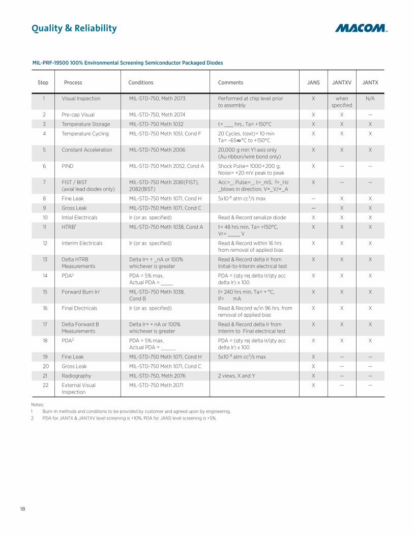
MIL-PRF-19500 100% Environmental Screening Semiconductor Packaged Diodes
1 Visual Inspection MIL-STD-750, Meth 2073 Performed at chip level prior X when N/Ato assembly specified
2 Pre-cap Visual MIL-STD-750, Meth 2074 X X —
3 Temperature Storage MIL-STD-750 Meth 1032 t= ___ hrs., Ta= +150°C X X X
4 Temperature Cycling MIL-STD-750 Meth 1051, Cond F 20 Cycles, t(ext)= 10 min X X XTa= -65∞°C to +150°C
5 Constant Acceleration MIL-STD-750 Meth 2006 20,000 g min Y1 axis only X X X(Au ribbon/wire bond only)
6 PIND MIL-STD-750 Meth 2052, Cond A Shock Pulse= 1000+200 g, X — —Noise= +20 mV peak to peak
7 FIST / BIST MIL-STD-750 Meth 2081(FIST), Acc=_, Pulse=_, t=_mS, f=_Hz X — —(axial lead diodes only) 2082(BIST) _blows in direction, V=_V,I=_A
8 Fine Leak MIL-STD-750 Meth 1071, Cond H 5x10⁻⁸ atm cc3/s max — X X
9 Gross Leak MIL-STD-750 Meth 1071, Cond C — X X
10 Intial Electricals Ir (or as specified) Read & Record serialize diode X X X
11 HTRB1 MIL-STD-750 Meth 1038, Cond A t= 48 hrs min, Ta= +150°C, X X XVr= ____ V
12 Interim Electricals Ir (or as specified) Read & Record within 16 hrs X X Xfrom removal of applied bias
13 Delta HTRB Delta Ir= + _nA or 100% Read & Record delta Ir from X X XMeasurements whichever is greater Initial-to-Interim electrical test
14 PDA2 PDA = 5% max, PDA = (qty rej delta Ir/qty acc X X XActual PDA = ____ delta Ir) x 100
15 Forward Burn In1 MIL-STD-750 Meth 1038, t= 240 hrs min, Ta= + °C, X X XCond B If= mA
16 Final Electricals Ir (or as specified) Read & Record w/in 96 hrs. from X X Xremoval of applied bias
17 Delta Forward B Delta Ir= + nA or 100% Read & Record delta Ir from X X XMeasurements whichever is greater Interim to Final electrical test
18 PDA2 PDA = 5% max, PDA = (qty rej delta Ir/qty acc X X XActual PDA = _____ delta Ir) x 100
19 Fine Leak MIL-STD-750 Meth 1071, Cond H 5x10⁻⁸ atm cc3/s max X — —
20 Gross Leak MIL-STD-750 Meth 1071, Cond C X — —
21 Radiography MIL-STD-750, Meth 2076 2 views, X and Y X — —
22 External Visual MIL-STD-750 Meth 2071 X — —Inspection
Quality & Reliability
Notes:1 Burn-In methods and conditions to be provided by customer and agreed upon by engineering.2 PDA for JANTX & JANTXV level screening is +10%; PDA for JANS level screening is +5%.
18
Space_HiRel brochure_051316_final_Space_HiRel brochure_040316 5/22/16 1:44 PM Page 20

Quality & Reliability
19
Group B Inspection Sample Size 1, 2 Conditions Comments JANS JANTXV JANTX
MIL-PRF-19500 Group B Conformance Inspection
Subgroup 14 Electrical rejects may be used
Physical Dimensions 22 (8) MIL-STD-750 Meth 2066 Specified case outline dimensions X — —
Subgroup 24 Electrical rejects may be used
Solderability 15 (6) leads MIL-STD-750 Meth 2026 Leads from a minimum of X X X3 devices shall be tested
Resistance to Solvents 15 (6) MIL-STD-750 Meth 1022 X X X
Subgroup 34
Temperature Cycling 22 (6) MIL-STD-750 Meth 1051, 45 Cycles including screening, X X XCond F text = 10 min Ta= -65°C to
+150°C (JANS 100 cycles)
Thermal Shock 22 (6) MIL-STD-750 Meth 1056, 10 cycles (JANS 25 cycles) X X XCond B (glass axial lead only)
Surge 22 (6) Only when specified X X X
Fine Leak 22(6) MIL-STD-750, Meth 1071, 5x10⁻⁸ atm cc3/s max X X XCond H
Gross Leak 22 (6) MIL-STD-750 Meth 1071, X X XCond C
Electrical Tests3 22 (6) Read & Record X X X
Intermittent 22 (12) MIL-STD-750 Meth 1037, Submit to 6000 cycles to satisfy — X XOperating Life 2000 cycles Group C Subgroup 6 requirement
Electrical Tests3 22 (12) Read & Record — X X
De-cap Internal Visual 6 (6) MIL-STD-750 Meth 2075 Decap devices X X X
Bond Strength 22 (12) wires or MIL-STD-750 Meth 2037 Use for die shear X X X1 (6) devices
SEM 22 (12) MIL-STD-750, METH 2077 When specified X X X
Die Shear 11 (6) MIL-STD-750, METH 2017 Use bond pull samples X — —
Subgroup 44
Intermittent 22 (12) MIL-STD-750 Meth 1037, Submit to 6000 cycles to satisfy X — —Operating Life 2000 cycles Group C Subgroup 6 requirement
Electrical Tests 22 (12) Read & Record satisfy X — —with Group C Subgroup 6
Subgroup 54
Accelerated Steady 22 (12) MIL-STD-750, Meth 1027 t= 96 hrs., Ta= +275°C Vr= V(pk), X — —State Life *Schottky= Tj max, 240 hrs. lo= mA, f= Hz
Electrical Tests3 22 (12) Read & Record X — —
Subgroup 64
Thermal Resistance 22 (8) MIL-STD-750 Meth 408 Read & Record X X X(Meth 3101 option JANS)
High Temp Life 22 (12) MIL-STD-750 Meth 1032 t= 340 hrs, Ta= T STG(MAX) N/A X X(Non-operating)
Electrical Tests3 22 (12) Read & Record N/A X X
Notes:1 Small lot sample size defined in parentheses ( ). Inspection lot quantity shall not exceed 2,500 pcs for JANTX & JANTXV
Group A small lot sampling; inspection lot quantity shall not exceed 1,000 pcs for JANS Group A small lot sampling.Group B small lot sampling: inspection lot quantity shall not exceed 1,000 pcs for JANS Group B small lot sampling.
2 Electrical test parameters shall be defined by product type and specific requirements; test limits at temperature may vary from those published in this catalog.3 Endpoint electrical tests parameters shall be defined by product type and specific requirements. 4 Test sequence may differ according to JAN screening level.
Space_HiRel brochure_051316_final_Space_HiRel brochure_040316 5/22/16 1:44 PM Page 21

Quality & Reliability
20
Notes:
1 Small lot sample size defined in parentheses ( ). Inspection lot quantity shall not exceed 2,500 pcs for JANTX & JANTXV Group A small lot sampling;inspection lot quantity shall not exceed 1,000 pcs for JANS Group A small lot sampling.
2 Electrical test parameters shall be defined by product type and specific requirements; test limits at temperature may vary from those publishedin this catalog.
Group C Inspection Sample Size 1, 2 Conditions Comments
MIL-PRF-19500 Group C Conformance Inspection (all levels)
Subgroup 1
Physical Dimensions 15 (6) MIL-STD-750, Meth 2066
Subgroup 2
Thermal Shock 22 (6) MIL-STD-750 Meth 1056, Cond A Glass axial lead only
Terminal Strength 22 (6) MIL-STD-750 Meth 2036, Cond E Leaded packages only, w=___oz.; t=___sec
Fine Leak 22 (6) MIL-STD-750 Meth 1071, Cond H 5x10⁻⁸ atm cc3/s max
Gross Leak 22 (6) MIL-STD-750 Meth 1071, Cond C
Moisture Resistance 22 (6) MIL-STD-750, Meth 1021 Omit initial conditioning
End-point Electricals2 22 (6) Read & Record
Subgroup 3
Shock 22 (6) MIL-STD-750 Meth 2016 Non-operating,1500G, 0.5ms, 5 blows X1, Y1, Z1
Variable Frequency 22 (6) MIL-STD-750 Meth 2056
Acceleration 22 (6) MIL-STD-750 Meth 2006 1 minute min, 20K g X1, Y1, Z1
End-point Electricals2 22 (6) Read & Record
Subgroup 4
Salt Atmosphere 15 (6) MIL-STD-750, Meth 1041 Electrical rejects may be used
Subgroup 5
Thermal Resistance 15 (6) MIL-STD-750, Meth 4081 Read & Record
Subgroup 6
Intermittent Operating Life 22 (12) MIL-STD-750, Meth 1037 Units from Group B-2000 cycle test may be used6000 cycles to complete the 6000 cycles
End-point Electricals2 22 (12) Read & Record
Bond Strength 11 wires MIL-STD-750 Meth 2037 Only when Group B units continue to satisfy Group Crequirement, Read & Record
Subgroup 7
Internal Water Vapor 3 MIL-STD-750, Meth 1018 3 devices c= 0 or 5 devices c= 1
Space_HiRel brochure_051316_final_Space_HiRel brochure_040316 5/22/16 1:44 PM Page 22

Quality & Reliability
Step Process MIL-STD-883 Test Method Comments K H
MIL-PRF-38534 100% Environmental Screening Hybrid Devices & MMICs
1 Non Destruct Bond Pull 2023 X —
2 Internal Visual 017 X X
3 Temperature Cycling 1051 Cond. C; 10 Cycles X X
4 Constant Acceleration 2001 Cond B; Y1 Only X X
5 PIND 2020 Cond A X Optional
6 Pre Burn-In Electrical Test In accordance with device specification Read & Record, serialize X X
7 Burn-In 1015 X —
10 Interim Electricals In accordance with device specification Read & Record X —
11 Burn-In 1015 X X
12 Final Electricals In accordance with device specification Read & Record X X
13 Fine Leak 1014 X X
14 Gross Leak 1014 X X
15 Radiography 2012 2 views, X and Y X —
16 External Visual Inspection 2009 X X
Group B Inspection Sample Size 1, 2 MIL-STD-883 Test Method Comments
MIL-PRF-38534 Group B Performance Inspection
Subgroup 1 2 (0)
Physical Dimensions 2016
Subgroup 3 3 (0)
Resistance to Solvents 2015
Subgroup 4 1 (0)
Internal Visual and Mechanical 2014
Subgroup 5 2 (0)
Bond Strength 2011 Condition C; 100 cycles
Subgroup 6 2 (0)
Die Shear Strength 2019
Subgroup 7 1 (0)
Solderability 2003 Solder Temperature +245° C + 5°C
Subgroup 8 5 (0)
Fine Leak 1014 Class H only
Gross Leak 1014 Class H only
Notes:1 Burn-In methods and conditions to be provided by MACOM. If provided by customer, MACOM reserves the right to review and approve conditions.2 PDA for Class H is 10% or 1 device. Class K is 2% or 1 device.
Notes:1 Small lot sample size with defects allowed provided in parentheses ( ).2. Electrical test parameters shall be defined by product type and specific requirements; test limits at temperature may vary from those published in this catalog.
21
Space_HiRel brochure_051316_final_Space_HiRel brochure_040316 5/22/16 1:44 PM Page 23

Quality & Reliability
Notes:1 Small lot sample size with defects allowed provided in parentheses ( ).2 Electrical test parameters shall be defined by product type and specific requirements; test limits at temperature may vary from those published in this catalog.
Group C Inspection Sample Size 1, 2 MIL-STD-883 Test Method Comments
MIL-PRF-38534 Group C Performance Inspection (all levels)
Subgroup 1 5 (0)
Resistance to Soldering Heat 2036
External Visual 2009
PIND 2020 Condition A
Temperature Cycle 1010 Condition C; 100 cycles
Mechanical shock 2002 B, Y1 direction
Constant Acceleration 2001 5000 g, Y1 direction
Random Vibration 2026 Condition A
Fine Leak 1014
Gross Leak 1014
PIND 2020 A, 1 pass
Visual Examination 1010 Omit initial conditioning
End-point Electricals2 Read & Record
Subgroup 2 5 (0)
Steady State Life Test 1005 1,000 hours at +125°C or equivalent
End-point Electricals2 Read & Record
Subgroup 3 3 (0) or 5(1)
Internal Water Vapor 1018
Subgroup 4 2 (0
Internal Visual 2017
Wire Bond Strength 2011
Element Shear 2019 or 2027
Subgroup 5 3 (0
End-point Electricals2 Group A-1
ESDS 3015
End-point Electricals2 Group A-1
Group D Inspection Sample Size 1, 2 MIL-STD-883 Test Method Comments
MIL-PRF-38534 Group D Performance Inspection
Subgroup 1
Thermal Shock 5 (0) 2016 Condition C
Stabilization Bake 5 (0) 1008 +150°C, 1 hour
Lead Integrity 1 (0) 2004
Fine Leak 5 (0) 1014 Condition A or B
Gross Leak 5 (0) 1014 Condition C or D
Subgroup 3
Salt Atmosphere 5 (0) 1009 Condition A
Subgroup 4
Metal Package Isolation 3 (0) 1003 600 V dc, 100 nA maximum22
Space_HiRel brochure_051316_final_Space_HiRel brochure_040316 5/22/16 1:44 PM Page 24

Quality & Reliability
1016 Insulation Resistance
1020 ESD Test Method
1021 Moisture Resistance
1022 Resistance to Solvents
1026 Steady-State Operation Life
1027 Steady-State Operation Life (sample plan)
1031 High Temperature Life Non-Operating
1032 High Temperature Life (non-operating)
1033 A, B Reverse Voltage Leakage Stability
1037 Intermittent Operation Life
1038 A, B HTRB Burn-In & Power Burn-In
1039 A, B HTRB Power Burn-In
1040 A, B Burn-In (Thyristors Controlled Rectifiers) / Blocking Voltage Test
1041 Salt Atmosphere
1048 Blocking Life
1051 A, F, G Temp Cycling (Air-to-Air) and LN2
1054 Potted Environment Stress Test
1055 Monitored Mission
1056 A, B, D Thermal Shock
1057 B Glass Cracking
1071 A, B, E, G1 Hermetic Seal
1081 Dielectric Withstanding Voltage
2005 Axial Lead Tensile Test
2006 A thru E Constant Acceleration
2017 A Die Attach Integrity (Die Shear)
2026 Solderability
2031 A, B Resistance to Soldering Heat
2036 A, E Terminal Strength
2037 D Bond Strength (Destructive Bond Pull Test)
2038 Surface Mount End Cap Bond Integrity
2052 A PIND Test
2066 Physical Dimensions
2068 Visual Inspection for NonTransparent Devices
2071 Visual and Mechanical Inspection
2072 Internal Visual Inspection (Pre-Cap)
2073 Chip and Die Visual Inspection
2074 Internal Visual Inspection
2075 Decap Internal Visual Design Verification
2078 Internal Visual For Wire Bonded Diodesand Rectifiers
2101SB DPA Procedures for Diodes(Scribe and Break only)
3001 Breakdown Voltage, Collector to Base
3011 Breakdown Voltage, Collector to Emitter
3036 Collector to Base Cutoff Current
3041 Collector to Emitter Cutoff Current
3051 Safe Operating Area
3053 Safe Operating Area (Switching)
3061 Emitter to Base Cutoff Current
3066 Base Emitter Voltage (saturated or nonsaturated)
3071 Saturation Voltage and Resistance
3076 Forward-Current Transfer Ratio
3100 Junction Temperature Measurement
3101 Thermal Impedance Testing of Diodes
3131 Thermal Impedance Testing of Transistors
3181 Thermal Resistance for Thyristors
3201 Small-Signal, Short-Circuit Input Impedance
3206 Small-Signal, Short-Circuit Forward-Current Transfer Ratio
3211 Small-Signal, Short-Circuit Reverse-Voltage Transfer Ratio
3216 Small-Signal, Open-Circuit Output Admittance
3236 Cobo Measurement
3240 Cibo Measurement
3246 Noise Figure
3251 A, B Pulse Response Measurement
3306 Frequency Response
3401 Breakdown Voltage, Gate-to-Source
3403 Gate-to-Source Voltage or Current
3405 Drain-to-Source On-State Voltage
3407 Breakdown Voltage, Drain-to-Source
3411 Gate Reverse Current
3413 Drain Current
3421 Static Drain-to-Source On-State Resistance
3423 Small-Signal, Drain-to-Source On-State Resistance
4001 Capacitance
4011 Forward Voltage
4016 Reverse Current Leakage
4021 Breakdown Voltage (Diodes)
4022 BreakdownVoltage (Voltage Regulators Diodes)and Voltage-Reference
4023 A, B Scope Display
4026 Forward Recovery, Voltage and Time
4031 A, B Reverse Recovery TRR
4051 Small-Signal Reverse Breakdown Impedance
4065 Peak Reverse Power Test
4066 A1, A2, B Test Procedure Surge Current
4071 Temperature Coefficient of Breakdown Voltage
4081 Thermal Resistance of Diodes(Forward Voltage, Switching Method)
4201 Holding Current
4206 Forward Blocking Current
4211 Reverse Blocking Current
4219 Reverse Gate Current
4221 Gate-Trigger Voltage
4226 Forward On Voltage
Test Test Method Condition MIL-STD-750 Method Title
Test Test Method Condition MIL-STD-750 Method Title
Macom is qualified to perform the following MIL-STD-750 test methods
23
Space_HiRel brochure_051316_final_Space_HiRel brochure_040316 5/22/16 1:44 PM Page 25

Diodes for Hi-Rel Applications
Part Number1
Nominal Zener2
Voltage, VZ
(V)
Zener Test Current, IZT
(µA)
Max Zener3 Impedance, ZZT
(Ohms)
Max ReverseCurrent, IR @ VR
(µ
Max Noise Density, ND @ IZT
(µV / √ Hz)
Max ZenerDC Current, IZM
(mA)
1N4614-1, 1N4614UR-1 1.8 250 1200 7.5 1 1 120
1N4615-1, 1N4615UR-1 2 250 1250 5 1 1 110
1N4616-1, 1N4616UR-1 2.2 250 1300 4 1 1 100
1N4617-1, 1N4617UR-1 2.4 250 1400 2 1 1 95
1N4618-1, 1N4618UR-1 2.7 250 1500 1 1 1 90
1N4619-1, 1N4619UR-1 3 250 1600 0.8 1 1 87
1N4620-1, 1N4620UR-1 3.3 250 1650 7.5 1.5 1 85
1N4621-1, 1N4621UR-1 3.6 250 1700 7.5 2 1 83
1N4622-1, 1N4622UR-1 3.9 250 1650 5 2 1 80
1N4623-1, 1N4623UR-1 4.3 250 1600 4 2 1 77
1N4624-1, 1N4624UR-1 4.7 250 1550 10 2 1 75
1N4625-1, 1N4625UR-1 5.1 250 1500 10 3 2 70
1N4626-1, 1N4626UR-1 5.6 250 1400 10 4 4 65
1N4627-1, 1N4627UR-1 6.2 250 1200 10 5 5 61
1N4099-1, 1N4099UR-1 6.8 250 200 10 5.17 40 56
1N4100-1, 1N4100UR-1 7.5 250 200 10 5.7 40 51
1N4101-1, 1N4101UR-1 8.2 250 200 1 6.24 40 46
1N4102-1, 1N4102UR-1 8.7 250 200 1 6.61 40 44
1N4103-1, 1N4103UR-1 9.1 250 200 1 6.92 40 42
1N4104-1, 1N4104UR-1 10 250 200 1 7.6 40 38
1N4105-1, 1N4105UR-1 11 250 200 0.05 8.44 40 35
1N4106-1, 1N4106UR-1 12 250 200 0.05 8.12 40 32
1N4107-1, 1N4107UR-1 13 250 200 0.05 9.857 40 29
1N4108-1, 1N4108UR-1 14 250 200 0.05 10.65 40 27
1N4109-1, 1N4109UR-1 15 250 100 0.05 11.4 40 25
1N4110-1, 1N4110UR-1 16 250 100 0.05 12.15 40 24
1N4111-1, 1N4111UR-1 17 250 100 0.05 12.92 40 22
1N4112-1, 1N4112UR-1 18 250 100 0.05 13.67 40 21
1N4113-1, 1N4113UR-1 19 250 150 0.05 14.44 40 20
1N4114-1, 1N4114UR-1 20 250 150 0.01 15.2 40 19
1N4115-1, 1N4115UR-1 22 250 150 0.01 16.72 40 17
1N4116-1, 1N4116UR-1 24 250 150 0.01 18.25 40 16
1N4117-1, 1N4117UR-1 25 250 150 0.01 19 40 15
1N4118-1, 1N4118UR-1 27 250 150 0.01 20.45 40 14
1N4119-1, 1N4119UR-1 29 250 200 0.01 21.28 40 14
1N4120-1, 1N4120UR-1 30 250 200 0.01 22.8 40 13
1N4121-1, 1N4121UR-1 33 250 200 0.01 25.08 40 12
1N4122-1, 1N4122UR-1 36 250 200 0.01 27.38 40 11
1N4123-1, 1N4123UR-1 39 250 200 0.01 29.65 40 9.8
1N4124-1, 1N4124UR-1 43 250 250 0.01 32.65 40 8.9
1N4125-1, 1N4125UR-1 47 250 250 0.01 35.75 40 8.1
1N4126-1, 1N4126UR-1 51 250 300 0.01 38.76 40 7.5
1N4127-1, 1N4127UR-1 56 250 300 0.01 42.6 40 6.7
1N4128-1, 1N4128UR-1 60 250 400 0.01 45.6 40 6.4
1N4129-1, 1N4129UR-1 62 250 500 0.01 47.1 40 6.1
1N4130-1, 1N4130UR-1 68 250 700 0.01 51.68 40 5.6
1N4131-1, 1N4131UR-1 75 250 700 0.01 57 40 5.1
1N4132-1, 1N4132UR-1 82 250 800 0.01 62.32 40 4.6
N
Density,
ZenerD
Zener Diodes: 1N4099-1 to 1N4627-1, available in JAN, JANTX, JANTXV and JANS per/435
(table continued on page 25)
24
Space_HiRel brochure_051316_final_Space_HiRel brochure_040316 5/22/16 1:44 PM Page 26

25
Diodes for Hi-Rel Applications
Density,
N
Part Number1
Nominal Zener2
Voltage, VZ
(V)
Zener Test Current, IZT
(µA)
Max Zener3 Impedance, ZZT
(Ohms)
Max ReverseCurrent, IR @ VR
(µ
Max Noise Density, ND @ IZT
(µV / √ Hz)
Max ZenerDC Current, IZM
(mA)
1N4133-1, 1N4133UR-1 87 250 1000 0.01 66.12 40 4.4
1N4134-1, 1N4134UR-1 91 250 1200 0.01 69.16 40 4.2
1N4135-1, 1N4135UR-1 100 250 1500 0.01 76 40 3
Electrical specifications @ TA = +25°C (unless otherwise specified).
Note 1: The JEDEC type numbers shown have a ±5% tolerance on nominal Zener voltage. The su!x C is used to identify ±2%: and su!x D is used to identify ±1%.Note 2: Zener voltage is measured with the device junction in thermal equilibrium at an ambient temperature of 25°C + 3°C.Note 3: Zener impedance is derived by superimposing on IZT A 60 Hz rms a.c. current equal to 10% of IZT.
Zener Diodes: 1N4099-1 to 1N4627-1, available in JAN, JANTX, JANTXV and JANS per/435 (continued)
Zener Diodes: 1N746A-1 to 1N759A-1; 1N4307A-1 to 1N4372A-1, available in JAN, JANTX, JANTXV per /127
Part Number1
VZ @ (V)
Zener Test Current IZT
(mA)
Max Zener3 Impedance
(Ohms)Max Reverse Current, IR @ VR
(µMax Zener Current, IZM
(V)
1N4370A-1, 1N4370AUR-1 2.4 20 30 100 1 155
1N4371A-1, 1N4371AUR-1 2.7 20 30 60 1 140
1N4372A -1, 1N4372AUR-1 3 20 29 30 1 125
1N746A-1, 1N746AUR-1 3.3 20 28 5 1 120
1N747A-1, 1N747AUR-1 3.6 20 24 3 1 110
1N748A-1, 1N748AUR-1 3.9 20 23 2 1 100
1N749A-1, 1N749AUR-1 4.3 20 22 2 1 90
1N750A-1, 1N750AUR-1 4.7 20 19 5 1.5 85
1N751A-1, 1N751AUR-1 5.1 20 17 5 2 75
1N752A-1, 1N752AUR-1 5.6 20 11 5 2.5 70
1N753A-1, 1N753AUR-1 6.2 20 7 5 3.5 65
1N754A,-1, 1N754AUR-1 6.8 20 5 2 4 60
1N755A-1, 1N755AUR-1 7.5 20 6 2 5 55
1N756A-1, 1N756AUR-1 8.2 20 8 1 6 50
1N757A-1, 1N757AUR-1 9.1 20 10 1 7 45
1N758A-1, 1N758AUR-1 10 20 17 1 8 40
1N759A-1, 1N759AUR-1 12 20 30 1 9 35
Electrical specifications @ TA = +25°C (unless otherwise specified).
Note 1: Zener voltage tolerance on “A” sux is ±5%. No sux denotes ±10% tolerance, “C” sux denotes ±2% tolerance and “D” sux denotes ±1% tolerance.Note 2: Zener voltage is measured with the device junction in thermal equilibrium at an ambient temperature of 25°C + 3°C.Note 3: Zener impedance is derived by superimposing on IZT A 60 Hz rms a.c. current equal to 10% of IZT.
Th
Nominal Zener2 VoltageI ZT Z ZT @ I ZT
Space_HiRel brochure_051316_final_Space_HiRel brochure_040316 5/22/16 1:44 PM Page 27

Diodes for Hi-Rel Applications
26
Part Number1
Nominal Zener2
Voltage, VZ
(V)
Zener Test Current, IZT
(mA)
Max Zener3 Impedance
ZZT @ IZT
(Ohms)
Max Zener3
Knee Impedance ZZT @ IZT
Max DC Zener Current, IZM
(mA)
Max SurgeCurrent, IZSM
(mA)
Max Reverse Leakage, TA = 25°C, IR @ VR
Max TemperatureCoe!cientαVZ (%/°C)(Ohms) (mA) (µA) (V)
1N957B-1 6.8 18.5 4.5 700 1 55 300 150 5.2 0.05
1N958B-1 7.5 16.5 5.5 700 0.5 50 275 75 5.7 0.058
1N959B-1 8.2 15 6.5 700 0.5 45 250 50 6.2 0.065
1N960B-1 9.1 14 7.5 700 0.5 41 225 25 6.9 0.068
1N961B-1 10 12.5 8.5 700 0.25 38 200 10 7.6 0.075
1N962B-1 11 11.5 9.5 700 0.25 35 590 1 8.4 0.073
1N963B-1 12 10.5 11.5 700 0.25 32 540 1 9.1 0.076
1N964B-1 13 9.5 13 700 0.25 30 500 0.5 9.9 0.079
1N965B-1 15 8.5 16 700 0.25 26 433 0.5 11 0.082
1N966B-1 16 7.8 17 700 0.25 25 406 0.5 12 0.083
1N967B-1 18 7 21 750 0.25 21 361 0.5 14 0.085
1N968B-1 20 6.2 25 750 0.25 19 325 0.5 15 0.086
1N969B-1 22 5.6 29 750 0.25 17 295 0.5 17 0.087
1N970B-1 24 5.2 33 750 0.25 16 271 0.5 18 0.088
1N971B-1 27 4.6 41 750 0.25 14 240 0.5 21 0.09
1N972B-1 30 4.2 49 1000 0.25 13 216 0.5 23 0.091
1N973B-1 33 3.8 58 1000 0.25 12 197 0.5 25 0.092
1N974B-1 36 3.4 70 1000 0.25 11 180 0.5 27 0.093
1N975B-1 39 3.2 80 1000 0.25 9.1 166 0.5 30 0.094
1N976B-1 43 3 93 1000 0.25 8.8 151 0.5 33 0.095
1N977B-1 47 2.7 105 1500 0.25 7.9 138 0.5 36 0.095
1N978B-1 51 2.5 125 1500 0.25 7.4 127 0.5 39 0.096
1N979B-1 56 2.2 150 2000 0.25 6.9 116 0.5 43 0.096
1N980B-1 62 2 185 2000 0.25 6 105 0.5 47 0.097
1N981B-1 68 1.8 230 2000 0.25 5.5 95 0.5 52 0.097
1N982B-1 75 1.7 270 2000 0.25 5.1 86 0.5 56 0.098
1N983B-1 82 1.5 330 3000 0.25 4.6 79 0.5 62 0.098
1N984B-1 91 1.4 400 3000 0.25 4.2 71 0.5 69 0.099
1N985B-1 100 1.3 500 3000 0.25 3.7 65 0.5 76 0.11
1N986B-1 110 1.1 750 4000 0.25 3.3 59 0.5 84 0.11
Electrical specifications @ TA = +25°C (unless otherwise specified).
Note 1: The JEDEC type numbers shown (B Sux) have a ±5% tolerance on nominal Zener voltage. The sux A is used to identify ±10% tolerance; sux C is used to identify ±2%: and sux D is used to identify ±1%; no sux indicates ±20%.
Note 2: Zener voltage is measured with the device junction in thermal equilibrium at an ambient temperature of 25°C + 3°C.Note 3: Zener impedance is derived by superimposing on IZT A 60 Hz rms a.c. current equal to 10% of IZT.
Zener Diodes: 1N957B-1 to 1N986B-1, available in JAN, JANTX, JANTXV per /117
Space_HiRel brochure_051316_final_Space_HiRel brochure_040316 5/22/16 1:44 PM Page 28

27
Diodes for Hi-Rel Applications
Low Noise Zener Diodes: 1N5518B-1 to 1N5546B-1, available in JAN, JANTX and JANTXV per/437
Part Number1
Nominal Zener2
Voltage, VZ @ IZT
(V)
Zener Test Current, IZT
(mA)
Max Zener3 Impedance
B, C, D Su!x ZZT @ IZT
(Ohms)
Max ReverseCurrent, IRVR = Volts
Max ZenerDC Current,
IZM
(mA)
Max ReverseCurrent, IR @
VR
(µA) (V)
Max Noise Density, ND
@ IZT
(µV / √ Hz)Low VZ
Current, IZL(µA dc)(NON &
A- Su!x)(B- C-
D- Su!x)
1N5518B-1, 1N5518BUR-1 3.3 20 26 5 0.9 1 115 0.5 0.9 2
1N5519B-1, 1N5519BUR-1 3.6 20 24 3 0.9 1 105 0.5 0.9 2
1N5520B-1, 1N5520BUR-1 3.9 20 22 1 0.9 1 98 0.5 0.85 2
1N5521B-1, 1N5521BUR-1 4.3 20 18 3 1 1.5 88 0.5 0.75 2
1N5522B -1, 1N5522BUR-1 4.7 10 22 2 1.5 2 81 0.5 0.6 1
1N5523B-1, 1N5523BUR-1 5.1 5 26 2 2 2.5 75 0.5 0.65 0.25
1N5524B-1, 1N5524BUR-1 5.6 3 30 2 3 3.5 68 1 0.3 0.25
1N5525B-1, 1N5525BUR-1 6.2 1 30 1 4.5 5 61 1 0.2 0.01
1N5526B-1, 1N5526BUR-1 6.8 1 30 1 5.5 6.2 56 1 0.1 0.01
1N5527B -1, 1N5527BUR-1 7.5 1 35 0.5 6 6.8 51 2 0.05 0.01
1N5528B-1, 1N5528BUR-1 8.2 1 40 0.5 6.5 7.5 46 4 0.05 0.01
1N5529B-1, 1N5529BUR-1 9.1 1 45 0.1 7 8.2 42 4 0.05 0.01
1N5530B-1, 1N5530BUR-1 10 1 60 0.05 8 9.1 38 4 0.1 0.01
1N5531B-1, 1N5531BUR-1 11 1 80 0.05 9 9.9 35 5 0.2 0.01
1N5532B-1, 1N5532BUR-1 12 1 90 0.05 9.5 0.8 32 10 0.2 0.01
1N5533B-1, 1N5533BUR-1 13 1 90 0.01 10.5 11.7 29 15 0.2 0.01
1N5534B-1, 1N5534BUR-1 14 1 100 0.01 11.5 12.6 27 20 0.2 0.01
1N5535B-1, 1N5535BUR-1 15 1 100 0.01 12.5 13.5 25 20 0.2 0.01
1N5536B-1, 1N5536BUR-1 16 1 100 0.01 13 14.4 24 20 0.2 0.01
1N5537B-1, 1N5537BUR-1 17 1 100 0.01 14 15.3 22 20 0.2 0.01
1N5538B-1, 1N5538BUR-1 18 1 100 0.01 15 16.2 21 20 0.2 0.01
1N5539B-1, 1N5539BUR-1 19 1 100 0.01 16 17.1 20 20 0.2 0.01
1N5540B-1, 1N5540BUR-1 20 1 100 0.01 17 18 19 20 0.2 0.01
1N5541B-1, 1N5541BUR-1 22 1 100 0.01 18 19.8 17 20 0.25 0.01
1N5542B-1, 1N5542BUR-1 24 1 100 0.01 20 21.6 16 20 0.3 0.01
1N5543B-1, 1N5543BUR-1 25 1 100 0.01 21 22.4 15 20 0.35 0.01
1N5544B-1, 1N5544BUR-1 28 1 100 0.01 23 25.2 14 20 0.4 0.01
1N5545B-1, 1N5545BUR-1 30 1 100 0.01 24 27 13 20 0.45 0.01
1N5546B-1, 1N5546BUR-1 33 1 100 0.01 28 29.7 12 20 0.5 0.01
Electrical specifications @ TA = +25°C (unless otherwise specified).
Note 1: No su!x type numbers are ±20% with guaranteed limits for only VZ, lR, and VF. Units with “A” su!x are ±10% with guaranteed limits for VZ, lR, and VF. Units with guaranteed limits for all six parameters are indicated by a “B” su!x for ±5.0% units, “C” su!x for ±2.0% and “D” su!x for ±1.0%.
Note 2: Zener voltage is measured with the device junction in thermal equilibrium at an ambient temperature of 25°C + 3°C.Note 3: Zener impedance is derived by superimposing on IZT A 60 Hz rms a.c. current equal to 10% of IZT.
Density,
Space_HiRel brochure_051316_final_Space_HiRel brochure_040316 5/22/16 1:44 PM Page 29

28
TC Zener Diodes: 1N4565-1 to 1N4584-1, available in JAN, JANTX, JANTXV and JANS per /452
Diodes for Hi-Rel Applications
Part Number1Zener Test Current, IZT
(mA)
Eective TemperatureCoecient
(% / °C)
Voltage TemperatureStability (∆VZT)1
(mV)Temperature Range
(°C)
Maximum DynamicZener Impedance2
(Ohms)
1N4565-1, 1N4565UR-1 0.5 0.01 48 0 to +75°C 200
1N4565A-1, 1N4565AUR-1 0.5 0.01 100 -55 to +100°C 200
1N4566-1, 1N4566UR-1 0.5 0.005 24 0 to +75°C 200
1N4566A-1, 1N4566AUR-1 0.5 0.005 50 -55 to +100°C 200
1N4567-1, 1N4567UR-1 0.5 0.002 10 0 to +75°C 200
1N4567A-1, 1N4567AUR-1 0.5 0.002 20 -55 to +100°C 200
1N4568-1, 1N4568UR-1 0.5 0.001 5 0 to +75°C 200
1N4568A-1, 1N4568AUR-1 0.5 0.001 10 -55 to +100°C 200
1N4569-1, 1N4569UR-1 0.5 0.0005 2.5 0 to +75°C 200
1N4569A-1, 1N4569AUR-1 0.5 0.0005 5 -55 to +100°C 200
1N4570-1, 1N4570UR-1 1 0.01 48 0 to +75°C 100
1N4570A-1, 1N4570AUR-1 1 0.01 100 -55 to +100°C 100
1N4571-1, 1N4571UR-1 1 0.005 24 0 to +75°C 100
1N4571A-1, 1N4571AUR-1 1 0.005 50 -55 to +100°C 100
1N4572-1, 1N4572UR-1 1 0.002 10 0 to +75°C 100
1N4572A-1, 1N4572AUR-1 1 0.002 20 -55 to +100°C 100
1N4573-1, 1N4573UR-1 1 0.001 5 0 to +75°C 100
1N4573A-1, 1N4573AUR-1 1 0.001 10 -55 to +100°C 100
1N4574-1, 1N4574UR-1 1 0.0005 2.5 0 to +75°C 100
1N4574A-1, 1N4574AUR-1 1 0.0005 5 -55 to + 100°C 100
1N4575-1, 1N4575UR-1 2 0.01 48 0 to +75°C 50
1N4575A-1, 1N4575AUR 2 0.01 100 -55 to +100°C 50
1N4576, 1N4576UR 2 0.005 24 0 to +75°C 50
1N4576A, 1N4576AUR-1 2 0.005 50 -55 to +100°C 50
1N4577-1, 1N4577UR-1 2 0.002 10 0 to +75°C 50
1N4577A-1, 1N4577AUR-1 2 0.002 20 -55 to +100°C 50
1N4578-1, 1N4578UR-1 2 0.001 5 0 to + 75°C 50
1N4578A-1, 1N4578AUR-1 2 0.001 10 -55 to +100°C 50
1N4579-1, 1N4579UR-1 2 0.0005 2.5 0 to +75°C 50
1N4579A-1, 1N4579AUR-1 2 0.0005 5 -55 to +100°C 50
1N4580-1, 1N4580UR-1 4 0.01 48 0 to +75°C 25
1N4580A-1, 1N4580AUR-1 4 0.01 100 -55 to +100°C 25
1N4581-1, 1N4581UR-1 4 0.005 24 0 to +75°C 25
1N4581A-1, 1N4581AUR-1 4 0.005 50 -55 to +100°C 25
1N4582-1, 1N4582UR-1 4 0.002 10 0 to +75°C 25
1N4582A-1, 1N4582AUR-1 4 0.002 20 -55 to +100°C 25
1N4583-1, 1N4583UR-1 4 0.001 5 0 to +75°C 25
1N4583A-1, 1N4583AUR-1 4 0.001 10 -55 to +100°C 25
1N4584-1, 1N4584UR-1 4 0.0005 2.5 0 to +75°C 25
1N4584A-1, 1N4584AUR-1 4 0.0005 5 -55 to +100°C 25
Electrical specifications @ +25°C (unless otherwise specified).
Note 1: The maximum allowable change observed over the entire temperature range i.e., the diode voltage will not exceed the specified mV at any discrete temperature between the established limits, per JEDEC standard No. 5.
Note 2: Zener impedance is derived by superimposing on lZT A 60 Hz rms a.c. current equal to 10% of lZT.
Th
Space_HiRel brochure_051316_final_Space_HiRel brochure_040316 5/22/16 1:44 PM Page 30

29
Diodes for Hi-Rel Applications
TC Zener Diodes: 1N821-1 to 1N829-1, available in JAN, JANTX, JANTXV and JANS per /159
Th
Part NumberZener Test Current, IZT
(V)
Eective TemperatureCoecient
(mA)
Max Zener Impedance ZZT
1
(Ohms Ω)
Voltage TemperatureStability, ∆VZT
-55°C to + 100°C2
(mV)
Ecient Temperature Coecient
(% / °C)
1N821-1, 1N821UR-1 5.9 - 6.5 7.5 15 96 0.01
1N821A-1, 1N821AUR-1 5.9 - 6.5 7.5 10 96 0.01
1N822-1, 1N822UR-1 † 5.9 - 6.5 7.5 15 96 0.01
1N823-1, 1N823UR-1 5.9 - 6.5 7.5 15 48 0.005
1N823A-1, 1N823AUR-1 5.9 - 6.5 7.5 10 48 0.005
1N824-1, 1N824UR-1 † 5.9 - 6.5 7.5 15 48 0.005
1N825-1, 1N825UR-1 5.9 - 6.5 7.5 15 19 0.002
1N825A-1, 1N825AUR-1 5.9 - 6.5 7.5 10 19 0.002
1N826-1, 1N826UR-1 6.2 - 6.9 7.5 15 20 0.002
1N827-1, 1N827UR-1 5.9 - 6.5 7.5 15 9 0.001
1N827A-1, 1N827AUR-1 5.9 - 6.5 7.5 10 9 0.001
1N828-1, 1N828UR-1 6.2 - 6.9 7.5 15 10 0.001
1N829-1, 1N829UR-1 5.9 - 6.5 7.5 15 5 0.0005
1N829A-1, 1N829AUR-1 5.9 - 6.5 7.5 10 5 0.0005
† Double anode: electrical specifications apply under both bias polarities.
Electrical specifications @ +25°C (unless otherwise specified).
Note 1: Zener impedance is derived by superimposing on lZT A 60 Hz rms a.c. current equal to 10% of lZT.Note 2: The maximum allowable change observed over the entire temperature range i.e., the diode voltage will not exceed the specified mV at any discrete temperature
between the established limits, per JEDEC standard No. 5.
Space_HiRel brochure_051316_final_Space_HiRel brochure_040316 5/22/16 1:44 PM Page 31

30
Diodes for Hi-Rel Applications
Switching Diodes: 1N3600, 1N4150-1 available in JAN, JANTX and JANTXV per /231
Switching Diodes: 1N6638 to 1N6643, available in JAN, JANTX, JANTXV and JANS per /578 and /609
Part Number
(V) (V pk) (µA dc) (µA dc) (pF) (nA)(V dc min)
(V dc max)
(V dc min)
(V dc max)
(V dc min)
(V dc max)
(V dc min)
(V dc max)
(V dc min)
(V dc max)
1N3600 75 50 0.1 100 2.5 4.0 0.54 0.62 0.66 0.74 0.76 0.86 0.82 0.92 0.87 1.00
1N4150-1, 1N4150UR-1 75 50 0.1 100 2.5 4.0 0.54 0.62 0.66 0.74 0.76 0.86 0.82 0.92 0.87 1.00
Electrical specifications @ +25°C (unless otherwise specified).
V f4 I F
= 10
0 m
A dc
(p
ulse
d)
V BR I R
= 10
µA
V f3 I F
= 5
0 m
A dc
(p
ulse
d)
V f2 I F
= 10
mA
dc
V f1 I F
= 1
mA
dc
I R V R
= 5
0 Vd
c
T A
= 2
5°C
V RWM
I R2 V
R =
50
Vdc
T A
= 15
0°C
C I R
= 0
; f =
1 M
Hz
AC
sign
al =
50 m
V (p
-p)
t rr I R
= 10
- 10
0 m
A
I F
= 10
- 10
0 m
A
R L = 10
0 W
V f5
I F =
200
mA
dc
(p
ulse
d)
Part Number
(V) (V pk) (mA) (V dc) (V dc) (nsec) (nA) (µA) (µA) (µA) (pF) (pF)
1N914, 1N914UR 100 75 75 0.8 1.2 5 25 0.5 35 75 4 2.8
1N4148-1, 1N4148UR-1 100 75 200 0.8 1.2 5 35 0.5 35 75 4 2.8
Electrical specifications @ +25°C (unless otherwise specified).
Capa
citan
ce
@
0 V
V BR @
100
µA
I R3 V
R =
20
Vdc
T A
= 15
0°C
I R2 @
75
Vdc
I R1 @
20
Vdc
I OV RWM
V f1 I F
= 10
mA
V f2 I F
= 50
mA
t rr I R
= 10
mA
I F
= 10
mA
R L = 10
0 W
Capa
citan
ce
@
1.5
V
I R3 V
R =
20
Vdc
T A
= 15
0°C
V dc
Part Number
(V pk) (mA) (V pk)VFR
(V pk) (ns) (pF) (pF) (ns) (nA dc) (nA dc) (µA dc) (µA dc)(V dc min)
(V dc max)
(V dc max)
(mA pulsed)
1N6638 150 100 125 5 20 2.5 2 4.5 35 500 50 100 – 1.10.8
1.2–
20010
1N6639 100 10 75 5 10 2.5 – 4 – 100 – 90 – 1.2 1.3 500
1N6640 75 10 50 5 10 2.5 – 4 – 100 – 90 0.540.760.820.87
0.620.860.92
1
–––1.1
1 50 100 200
1N6641 75 10 50 5 10 3 – 5 – 100 – 90 – 1.1 1.2 200
1N6642 100 100 75 5 20 5 2.8 5 25 500 50 100 – 1 1.2
– 1.2
10 100
1N6643 75 100 50 5 20 5 2.8 6 50 500 75 100 – 1 1.2
– 1.4
10 100
Electrical specifications @ TA = +25°C (unless otherwise specified).
V F @ I F
I FV BR @
I R
I R4 V
R =
VRW
M
I R2 V
R =
20
V
T A =
150°
C
V R1 V
R =
VRW
M
V FR /
t rr @
I F
= 20
0 m
A
V RWM
C T1 V
R =
0.0
V
I R3 V
R =
20
V
T A =
150°
C
C T2 V
R =
1.5
Vt rr
I R =
10 m
A
I F =
10 m
A
V F2 @
I F
T A =
-55°
C
V dc
t
fr
Switching Diodes: 1N914, 1N4148-1 available in JAN, JANTX and JANTXV per /116
Space_HiRel brochure_051316_final_Space_HiRel brochure_040316 5/22/16 1:44 PM Page 32

31
Diodes for Hi-Rel Applications
Switching Diodes: 1N6638US to 1N6643US, available in JAN, JANTX, JANTXV and JANS per /578 and /609
Switching Diodes: 1N4454-1, available in JAN, JANTX and JANTXV per /144
Part Number
(V pk) (µA) (V pk)VFR
(V pk) (ns) (pF) (pF) (ns) (nA dc) (nA dc) (µA dc) ( (V dc min)
(V dc max)
(V dc max)
(mA pulsed)
1N6638U and US 150 100 125 5.0 20 2.5 2.0 4.5 35 500 50 100 – 1.10.8
1.2–
20010
101N6639U and US 100 10 75 5.0 10 2.5 – 4.0 – 100 – 90 – 1.2 1.3 500
1N6640U and US 75 10 50 5.0 10 2.5 – 4.0 – 100 – 90 0.540.760.820.87
0.620.860.921.0
–––1.1
1 50 100 200
1N6641U and US 75 10 50 5.0 10 3.0 – 5.0 – 100 – 90 – 1.1 1.2 200
1N6642U, US and UB 100 100 75 5.0 20 5.0 2.8 5.0 25 500 50 100 – 1.0 1.2
– 1.2
10 100
1N6643U and US 75 100 50 5.0 20 5.0 2.8 6.0 50 500 75 100 – 1.0 1.2
– 1.4
10 100
Electrical specifications @ TA = +25°C (unless otherwise specified).
V F @ I F
I FV BR @
I R
I R4 V
R =
VRW
M
I R2 V
R =
20
V T
A =
150°
C
V R1 V
R =
VRW
M
V FR /
t rr @
IF =
200
mA
V RWM
C T1 V R
= 0.0
V
I R3 V
R =
20
V T
A =
150°
C
C T2 V
R =
1.5
Vt rr
I R =
10 m
A I
F = 10
mA
V F2 @
I F T
A =
-55°
C
tfr
µA dc)
t
Part Number
Ambient Ambient V dc A max(°C) (IF mA)
(V dc) max (°C)
Ambient (°C) (IR µA)
(V dcmax)
(V dc max) (nsec) (nsec) (V pk) (pF) (pF)
1N4531-1 2525150-55
1010010
100
0.81.20.81.3
2525150150
20752075
0.0250.50035.075.0
25 100 100 25 5 20 5 4 2.8
V
V F V FR @
I F =
50
mA
t rr I R
= 10
mA
I F
= 10
mA
rec =
100
Ω
V BRI R T FR @
I F =
50
mA
Capa
citan
ce
@ 1.
5 V
Capa
citan
ce
@ 0
V
Part NumberVBR @ 5 µA
(V)VRWM
(V pk)IO
(mA)Vf1 IF = 10 mA Vf2 IF = 10 mA
(V dc)Trr
(nsec)IR1 @ 50 Vdc
(µA)
IR2 @ 75 Vdc TA = 150°C
(µA)
Capacitance@ 0 V(pF)
1N4454-1, 1N4454UR-1 75 50 200 0.8 0.7 4 0.1 100 20
Switching Diodes: 1N4531, available in JAN, JANTX and JANTXV per /116
Space_HiRel brochure_051316_final_Space_HiRel brochure_040316 5/22/16 1:44 PM Page 33

32
Diodes for Hi-Rel Applications
Current Regulator Diodes: 1N5283-1 to 1N5314-1; 1N7041-1 to 1N7055-1 available in JAN, JANTX, JANTXV and JANS per /463
Part Number
Regulator Current IP (mA) @ VS=25V
Max DynamicImpedance @ VS =
25VZS (M)1
Min Knee Impedance
@ VK = 6.0VZK (M)2
Max LimitingVoltage
@ IL = 0.8 lP (min)VL (V)
Peak OperatingVoltage
(V)Nominal Minimum Maximum
1N5283-1, 1N5283UR-1 0.22 0.198 0.242 25 2.75 1 100
1N5284-1, 1N5284UR-1 0.24 0.216 0.264 19 2.35 1 100
1N5285-1, 1N5285UR-1 0.27 0.243 0.297 14 1.95 1 100
1N5286-1, 1N5286UR-1 0.3 0.27 0.33 9 1.6 1 100
1N5287-1, 1N5287UR-1 0.33 0.297 0.363 8 1.35 1 100
1N5288-1, 1N5288UR-1 0.39 0.351 0.429 4.1 1 1.05 100
1N5289-1, 1N5289UR-1 0.043 0.387 0.473 3.3 0.87 1.05 100
1N5290-1, 1N5290UR-1 0.47 0.423 0.517 2.7 0.75 1.05 100
1N5291-1, 1N5291UR-1 0.56 0.504 0.616 1.9 0.56 1.1 100
1N5292-1, 1N5292UR-1 0.62 0.558 0.682 1.55 0.47 1.13 100
1N5293-1, 1N5293UR-1 0.68 0.612 0.748 1.35 0.4 1.15 100
1N5294-1, 1N5294UR-1 0.75 0.675 0.825 1.15 0.335 1.2 100
1N5295-1, 1N5295UR-1 0.82 0.738 0.902 1 0.29 1.25 100
1N5296-1, 1N5296UR-1 0.91 0.819 1.001 0.88 0.24 1.29 100
1N5297-1, 1N5297UR-1 1 0.9 1.1 0.8 0.205 1.35 100
1N5298-1, 1N5298UR-1 1.1 0.99 1.21 0.7 0.18 1.4 100
1N5299-1, 1N5299UR-1 1.2 1.08 1.32 0.64 0.155 1.45 100
1N5300-1, 1N5300UR-1 1.3 1.17 1.43 0.58 0.135 1.5 100
1N5301-1, 1N5301UR-1 1.4 1.26 1.54 0.54 0.115 1.55 100
1N5302-1, 1N5302UR-1 1.5 1.35 1.65 0.51 0.105 1.6 100
1N5303-1, 1N5303UR-1 1.6 1.44 1.76 0.475 0.092 1.65 100
1N5304-1, 1N5304UR-1 1.8 1.62 1.98 0.42 0.074 1.75 100
1N5305-1, 1N5305UR-1 2 1.8 2.2 0.395 0.061 1.85 100
1N5306-1, 1N5306UR-1 2.2 1.98 2.42 0.37 0.052 1.95 100
1N5307-1, 1N5307UR-1 2.4 2.16 2.54 0.345 0.044 2 100
1N5308-1, 1N5308UR-1 2.7 2.43 2.97 0.32 0.035 2.15 100
1N5309-1, 1N5309UR-1 3 2.7 3.3 0.3 0.029 2.25 100
1N5310-1, 1N5310UR-1 3.3 2.97 3.63 0.28 0.024 2.35 100
1N5311-1, 1N5311UR-1 3.6 3.24 3.96 0.265 0.02 2.5 100
1N5312-1, 1N5312UR-1 3.9 3.51 4.29 0.255 0.017 2.6 100
1N5313-1, 1N5313UR-1 4.3 3.87 4.73 0.245 0.014 2.75 100
1N5314-1, 1N5314UR-1 4.7 4.23 5.17 0.235 0.012 2.9 100
1N7048-1, 1N7048UR-1 5.1 4.59 5.61 100 4 3.67 80
1N7049-1, 1N7049UR-1 5.6 5.04 6.16 90 4 4.03 80
1N7050-1, 1N7050UR-1 6.2 5.58 6.82 80 3 4.46 70
1N7051-1, 1N7051UR-1 6.8 6.12 7.48 70 2 4.9 70
1N7052-1, 1N7052UR-1 7.5 6.75 8.25 50 1.5 5.4 60
1N7053-1, 1N7053UR-1 8.2 7.38 9.02 30 1.5 5.9 60
1N7054-1, 1N7054UR-1 9.1 8.19 10.01 20 1 6.55 50
1N7055-1, 1N7055UR-1 10 9 11.1 10 1 7.2 50
Electrical specifications @ +25°C (unless otherwise specified).
Note 1: ZS is derived by superimposing A 90 Hz RMS signal equal to 10% of VS on VSNote 2: ZK is derived by superimposing A 90 Hz RMS signal equal to 10% of VK on VK
Available In chip form.
S
Space_HiRel brochure_051316_final_Space_HiRel brochure_040316 5/22/16 1:44 PM Page 34

33
Diodes for Hi-Rel Applications
Zener Diode Chip Series: CD4099 to CD4135, available in JANHC and JANKC per /435
Ze
Ze
Part Number
Nominal Zener VoltageVZ @ IZT
1
(V)Zener Test Current, IZT
(µA)
Max Zener Impedance ZZT @ IZT
2
(Ohms)
Maximum Reverse Leakage Current, IR @ VR
(µA) (V)
CD4099 6.8 250 200 10 5.17
CD4100 7.5 250 200 10 5.7
CD4101 8.2 250 200 1 6.24
CD4102 8.7 250 200 1 6.61
CD4103 9.1 250 200 1 6.92
CD4104 10 250 200 1 7.6
CD4105 11 250 200 0.05 8.44
CD4106 12 250 200 0.05 9.12
CD4107 13 250 200 0.05 9.87
CD4108 14 250 200 0.05 10.65
CD4109 15 250 100 0.05 11.4
CD4110 16 250 100 0.05 12.15
CD4111 17 250 100 0.05 12.92
CD4112 18 250 100 0.05 13.67
CD4113 19 250 150 0.05 14.44
CD4114 20 250 150 0.01 15.2
CD4115 22 250 150 0.01 16.72
CD4116 24 250 150 0.01 18.25
CD4117 25 250 150 0.01 19
CD4118 27 250 150 0.01 20.46
CD4119 28 250 200 0.01 21.28
CD4120 30 250 200 0.01 22.8
CD4121 33 250 200 0.01 25.08
CD4122 36 250 200 0.01 27.38
CD4123 39 250 200 0.01 29.65
CD4124 43 250 250 0.01 32.56
CD4125 47 250 250 0.01 35.75
CD4126 51 250 300 0.01 38.76
CD4127 56 250 300 0.01 42.6
CD4128 60 250 400 0.01 45.6
CD4129 62 250 500 0.01 47.1
CD4130 68 250 700 0.01 51.68
CD4131 75 250 700 0.01 57
CD4132 82 250 800 0.01 62.32
CD4133 87 250 1000 0.01 66.12
CD4134 91 250 1200 0.01 69.16
CD4135 100 250 1500 0.01 76
Electrical specifications @ +25°C (unless otherwise specified).
Note 1: Zener voltage range equals nominal Zener voltage ± 5% for no sux types. Zener voltage is read using a pulse measurement, 10 milliseconds maximum. “C” sux = ± 2% and “D” sux = ± 1 %.
Note 2: Zener impedance is derived by superimposing on lZT a 60 Hz rms AC current equal to 10 % of IZT.
Space_HiRel brochure_051316_final_Space_HiRel brochure_040316 5/22/16 1:44 PM Page 35

34
Diodes for Hi-Rel Applications
Zener Diode Chip Series: CD4614 to CD4627, available in JANHC and JANKC per /435
Part Number
Nominal Zener VoltageVZ @ IZT
1
(V)Zener Test Current, IZT
(µA)
Max Zener Impedance ZZT @ IZT
2
(Ohms)Maximum Reverse Leakage Current, IR @ VR
(µA) (V)
CD4614 1.8 250 1200 7.5 1
CD4615 2 250 1250 5 1
CD4616 2.2 250 1300 4 1
CD4617 2.4 250 1400 2 1
CD4618 2.7 250 1500 1 1
CD4619 3 250 1600 0.8 1
CD4620 3.3 250 1650 7.5 1.5
CD4621 3.6 250 1700 7.5 2
CD4622 3.9 250 1650 5 2
CD4623 4.3 250 1600 4 2
CD4624 4.7 250 1550 10 3
CD4625 5.1 250 1500 10 3
CD4626 5.6 250 1400 10 4
CD4627 6.2 250 1200 10 5
Electrical specifications @ +25°C (unless otherwise specified).
Note 1: Zener voltage range equals nominal Zener voltage ± 5% for no sux types. Zener voltage is read using a pulse measurement, 10 milliseconds maximum. “C” sux = ± 2% and “D” sux = ± 1 %.
Note 2: Zener impedance is derived by superimposing on lZT a 60 Hz rms AC current equal to 10 % of IZT.
Ze
Ze
Ze
Part Number
Nominal Zener VoltageVZ @ IZT
1
(V)Zener Test Current, IZT
(mA)
Max Zener Impedance ZZT @ IZT
2
(Ohms)Maximum Reverse Leakage Current, IR @ VR
Max ZenerCurrent, IZM
(mA)(µA) (V)
CD4370A 2.4 20 30 100 1 155
CD4371A 2.7 20 30 75 1 140
CD4372A 3 20 29 50 1 125
CD746A 3.3 20 28 10 1 120
CD747A 3.6 20 24 5 1 110
CD748A 3.9 20 23 5 1 100
CD749A 4.3 20 22 2 1 90
CD750A 4.7 20 19 5 1.5 85
CD751A 5.1 20 17 5 2 75
CD752A 5.6 20 11 5 2.5 70
CD753A 6.2 20 7 5 3.5 85
CD754A 6.8 20 5 2 4 60
CD755A 7.5 20 6 2 5 55
CD756A 8.2 20 8 1 6 50
CD757A 9.1 20 10 1 7 45
CD758A 10 20 17 1 8 40
CD759A 12 20 30 1 9 35
Electrical specifications @ +25°C (unless otherwise specified).
Note 1: Zener voltage range equals nominal voltage ± 5% for “A” sux. No sux denotes ± 10%. “C” sux = ± 2% and “D” sux = ± 1%. Zener voltage is read using a pulse measurement, 10 milliseconds maximum.
Note 2: Zener impedance is derived by superimposing on lZT a 60 Hz rms a.c. current equal to 10 % of IZT.
Ze
Zener Diode Chip Series: CD746A to CD759A, CD4370A to CD4372A, available in JANHC and JANKC per /127
Space_HiRel brochure_051316_final_Space_HiRel brochure_040316 5/22/16 1:45 PM Page 36

35
Diodes for Hi-Rel Applications
Zener Diode Chip Series: CD5518B to CD5546B, available in JANHC and JANKC per /437
Part Number
Nominal Zener VoltageVZ @ IZT
1 (V)
Zener Test Current, IZT (mA dc)
Max ZenerImpedanceZZT @ IZT
2
(Ohms)
Max ReverseLeakage Current
IR(mA dc)
Max ReverseLeakage Current
VR (V)
VZ3
(V)
Low VZ Current,IZL
(mA dc)
CD5518B 3.3 20 26 5 1 0.9 2
CD5519B 3.6 20 24 3 1 0.9 2
CD5520B 3.9 20 22 1 1 0.9 2
CD5521B 4.3 20 18 3 1.5 0.75 2
CD5522B 4.7 10 22 2 2 0.6 1
CD5523B 5.1 5 26 2 2.5 0.65 0.25
CD5524B 5.6 3 30 2 3.5 0.3 0.25
CD55258 6.2 1 30 1 5 0.2 0.01
CD5526B 6.8 1 30 1 6.2 0.1 0.01
CD5527B 7.5 1 35 0.5 6.8 0.05 0.01
CD5528B 8.2 1 40 0.5 7.5 0.05 0.01
CD5529B 9.1 1 45 0.1 8.2 0.05 0.01
CD55308 10 1 60 0.05 9.1 0.1 0.01
CD5531B 11 1 80 0.05 9.9 0.2 0.01
CD5532B 12 1 90 0.05 10.8 0.2 0.01
CD5533B 13 0 90 0.01 11.7 0.2 0.01
CD5534B 14 1 100 0.01 12.6 0.2 0.01
CD5535B 15 1 100 0.01 13.5 0.2 0.01
CD5536B 16 1 100 0.01 14.4 0.2 0.01
CD5537B 17 1 100 0.01 15.3 0.2 0.01
CD5538B 18 1 100 0.01 16.2 0.2 0.01
CD5539B 19 1 100 0.01 17.1 0.2 0.01
CD5540B 20 1 100 0.01 18 0.2 0.01
CD5541B 22 1 100 0.01 19.8 0.25 0.01
CD5542B 24 1 100 0.01 21.6 0.3 0.01
CD5543B 25 1 100 0.01 22.4 0.35 0.01
CD5544B 28 1 100 0.01 25.2 0.4 0.01
CD5545B 30 1·0 100 0.01 27 0.45 0.01
CD5546B 33 1 100 0.01 29.7 0.5 0.01
Electrical specifications @ +25°C (unless otherwise specified).
Note 1: Su!x “B” voltage range equals nominal Zener voltage. ± 5%. Su!x “A” equals ± 10 %. “C” su!x = ± 2 % and “D” su!x= ± 1 %. No su!x equals ± 20 %. Zener voltage is read using a pulse measurement, 10 milliseconds maximum.
Note 2: Zener impedance is derived by superimposing on lZT a 60 Hz rms ac current equal to 10 % of IZT.Note 3: DVZ is the maximum di"erence between VZ-@ IZT and VZ at IZL measured with the device junction in thermal equilibnum at an ambient temperature of +25° ± 3°C.
RegulationFactor
Space_HiRel brochure_051316_final_Space_HiRel brochure_040316 5/22/16 1:45 PM Page 37

36
Diodes for Hi-Rel Applications
Zener Diode Chip Series: CD957B to CD986B, available in JANHC and JANKC per /117
Part Number
Nominal Zener Voltage, VZ
1
(V)
Zener Test Current, IZT
(mA)
Max Zener Impedance ZZT @ IZT
2
(Ohms)
Max Zener ImpedanceZZK @ IZK
2 Max DC ZenerCurrent, IZM
(mA)
Max Reverse Leakage Current, IR @ VR
(Ohms) (mA) (µA) (V)
CD957B 6.8 18.5 4.5 700 1 55 5 5.2
CD958B 7.5 16.5 5.5 700 0.5 50 5 5.7
CD959B 8.2 15 6.5 700 0.5 45 5 6.2
CD960B 9.1 14 7.5 700 0.5 41 5 6.9
CD961B 10 12.5 8.5 700 0.25 38 2 7.6
CD962B 11 11.5 9.5 700 0.25 32 1 8.4
CD963B 12 10.5 11.5 700 0.25 31 1 9.1
CD964B 13 9.5 13 700 0.25 28 0.5 9.9
CD965B 15 8.5 16 700 0.25 25 0.5 11
CD966B 16 7.8 17 700 0.25 24 0.5 12
CD967B 18 7 21 750 0.25 20 0.5 14
CD968B 20 6.2 25 750 0.25 18 0.5 15
CD969B 22 5.6 29 750 0.25 16 0.5 17
CD970B 24 5.2 33 750 0.25 15 0.5 18
CD971B 27 4.6 41 750 0.25 13 0.5 21
CD972B 30 4.2 49 1000 0.25 12 0.5 23
CD973B 33 3.8 58 1000 0.25 11 0.5 25
CD974B 36 3.4 70 1000 0.25 10 0.5 27
CD975B 39 3.2 90 1000 0.25 9.5 0.5 30
CD976B 43 3 93 1500 0.25 8.8 0.5 33
CD977B 47 2.7 105 1500 0.25 7.9 0.5 36
CD978B 51 2.5 125 1500 0.25 7.4 0.5 39
CD979B 56 2.2 150 2000 0.25 6.8 0.5 43
CD980B 62 2 185 2000 0.25 6 0.5 47
CD981B 68 1.8 230 2000 0.25 5.5 0.5 52
CD982B 75 1.7 270 2000 0.25 5 0.5 56
CD983B 82 1.5 330 3000 0 .25 4.6 0.5 62
CD984B 91 1.4 400 3000 0.25 4.1 0.5 69
CD985B 100 1.3 500 3000 0.25 3.7 0.5 76
CD986B 110 1.1 750 4000 0.25 3.3 0.5 84
Electrical specifications @ +25°C (unless otherwise specified).
Note 1: Zener voltage range equals nominal voltage ± 5% for “B” sux. “A” Sux denotes ± 10%. No sux denotes ± 20%. “C” sux = ± 2% and “D” sux = ± 1%. Zener voltage is read using a pulse measurement, 10 milliseconds maximum.
Note 2: Zener impedance is derived by superimposing on lZT a 60 Hz rms a.c. current equal to 10 % of IZT.
Th
Space_HiRel brochure_051316_final_Space_HiRel brochure_040316 5/22/16 1:45 PM Page 38

37
Diodes for Hi-Rel Applications
TC Zener Diode Chip Series: CD4565 to CD4584A, available in JANHC and JANKC per /452
Ze
Part NumberZener Test Current, IZT
(mA)
E!ective TemperatureCoe"cient
(% / °C)
Voltage TemperatureStability, ∆VZT Max
-55° to + 100°1 (Ohms)
Temperature Range (°C)
Max Zener Impedance, ZZT
2 (Ohms)
CD4565 0.5 0.01 48 0 to +75 °C 200
CD4565A 0.5 0.01 100 -55 to +100 °C 200
CD4566 0.5 0.005 24 0 to +75 °C 200
CD4566A 0.5 0.005 50 -55 to +100 °C 200
CD4567 0.5 0.002 10 0 to +75 °C 200
CD4567A 0.5 0.002 20 -55 to +100 °C 200
CD4568 0.5 0.001 5 0 to +75 °C 200
CD4568A 0.5 0.001 10 -55 to +100 °C 200
CD4569 0.5 0.0005 2.5 0 to +75 °C 200
CD4569A 0.5 0.0005 5 -55 to +100 °C 200
CD4570 1 0.01 48 0 to +75° C 100
CD4570A 1 0.01 100 -55 to +100 °C 100
CD4571 1 0.005 24 0 to +75°C 100
CD4571A 1 0.005 50 -55 to +100°C 100
CD4572 1 0.002 10 0 to +75°C 100
CD4572A 1 0.002 20 -55 to +100°C 100
CD4573 1 0.001 5 0 to +75 °C 100
CD4573A 1 0.001 10 -55 to +100 °C 100
CD4574 1 0.0005 2.5 0 to +75 °C 100
CD4574A 1 0.0005 5 -55 to +100 °C 100
CD4575 2 0.01 48 0 to +75°C 50
CD4575A 2 0.01 100 -55 to +100 °C 50
CD4576 2 0.005 24 0 to +75 °C 50
CD4576A 2 0.005 50 -55 to +100 °C 50
CD4577 2 0.002 10 0 to +75 °C 50
CD4577A 2 0.002 20 -55 to +100 °C 50
CD4578 2 0.001 5 0 to +75 °C 50
CD4578A 2 0.001 10 -55 to +100 °C 50
CD4579 2 0.0005 2.5 0 to +75 °C 50
CD4579A 2 0.0005 5 -55 to +100 °C 50
CD4580 4 0.01 48 0 to +75 °C 25
CD4580A 4 0.01 100 -55 to +100 °C 25
CD4581 4 0.005 24 0 to +75 °C 25
CD4581A 4 0.005 50 -55 to +100 °C 25
CD4582 4 0.002 10 0 to +75 °C 25
CD4582A 4 0.002 20 -55 to +100 °C 25
CD4583 4 0.001 5 0 to +75 °C 25
CD4583A 4 0.001 10 -55 to +100 °C 25
CD4584 4 0.0005 2.5 0 to +75° C 25
CD4584A 4 0.0005 5 -55 to +100 °C 25
Electrical specifications @ +25 °C (unless otherwise specified).
Note 1: The maximum allowable change observed over the entire temperature range, i.e., the diode voltage will not exceed the specialized mV at any discrete temperature between the established limits, per JEDEC standard No.5.
Note 2: Zener impedance is derived by superimposing on lZT a 60 Hz rms ac current equal to 10% of lZT.
Space_HiRel brochure_051316_final_Space_HiRel brochure_040316 5/22/16 1:45 PM Page 39

Diodes for Hi-Rel Applications
Ultrafast Rectifier Diode Chips: CD5802, CD5804 & CD5806, available in JANHC and JANKC per /477
Ultrafast Rectifier Diode Chips: CD5807, CD5809 & CD5811, available in JANHC and JANKC per /477
Silicon Switching Diode Chips: CD914, CD4148, CD4531, CD6642 & CD4454, available in JANHC and JANKC per /116 and /578
Part Number (V min) (V pk) (A) (ns) (pF) (V dc) (V dc) (V dc) (V dc) (µA dc) (µA dc) (V dc)
CD5802 50 60 25 25 25 0.875 0.975 0.800 1.075 1 175 2.2
CD5804 100 110 25 25 25 0.875 0.975 0.800 1.075 1 175 2.2
CD5806 150 160 25 25 25 0.875 0.975 0.800 1.075 1 175 2.2
Electrical specifications @ +25°C (unless otherwise specified).
I R @
VRW
M
Tc =
25°
C
V FRM
t r =
8 n
S,
IFM
= 2
50 m
A
V RVM
V BR I O TJ =
75°
CT rr
I F
= 0.
5 A,
I RM =
0.5
A,
I (
REC)
= 0
.05
AC j
(max
) @ V
R =
10.0
V
V FM1
I FM
= 1.
0 A,
T
P =
8.3
mS
(max
)V FM
2
I FM =
2.5
A,
T
P =
8.3
mS
(max
)
V FM3
I FM
= 1.
0 A,
T
A =
+12
5°C
V FM4
I FM
= 1.
0 A,
T
A =
-65°
C
I R2 @
VRW
M R
ated
TA =
125°
C
A T
Part Number (V min) (V pk) (A) (ns) (pF) (V dc) (V dc) (V dc) (V dc) (µA dc) (µA dc) (V dc)
CD5807 50 60 2.5 30 60 0.865 0.875 0.925 0.800 5 525 2.2
CD5809 100 110 2.5 30 60 0.865 0.875 0.925 0.800 5 525 2.2
CD5811 150 160 2.5 30 60 0.865 0.875 0.925 0.800 5 525 2.2
Electrical specifications @ +25°C (unless otherwise specified).
I R @
VRW
M T
c = 2
5°C
V FRM
t r =
8 n
S,
IFM
= 2
50 m
A
V RVM
V BR I O TJ =
75°
CT rr
I F
= 0.
5 A,
I RM =
0.5
A,
I (
REC)
= 0
.05
AC j (
max
) @ V
R =
10.0
V
V FM1
I FM
= 1.
0 A,
T
P =
8.3
mS
(max
)V FM
2
I FM =
2.5
A,
T
P =
8.3
mS
(max
)
V FM3
I FM
= 1.
0 A,
T
A =
+12
5°C
V FM4
I FM
= 1.
0 A,
T
A =
-65°
C
I R2 @
VRW
M R
ated
TA =
125°
C
A T
Part Number (V min) (V pk) (mA) (Vdc) (Vdc) (Vdc) (nsec) (nA) (µA @ V) (µA) (µA @ V) (pF) (pF)
CD914 100 75 75 0.8 1.2 N/A 5 25 0.5 @ 75 35 75 @ 75 4.0 2.8
CD4148CD4531CD6642
100 75 200 0.8 N/A 1.2 5 35 0.5 @ 75 35 75 @ 75 4.0 2.8
CD4454 75 50 200 1.0 N/A N/A 4 N/A 0.1 @ 50 N/A 100 @ 50 2.0 N/A
Electrical specifications @ +25°C (unless otherwise specified).
V BR @
100
mA
I R4 T A
= 15
0°C
I R1 @
20
Vdc
V RVM
I R3 @
20
Vdc
T A
= 15
0°C
Capa
cita
nce
@
0 V
V F1
I F =
10 m
AV F2
I F
= 50
mA
V F3
I F =
100
mA
Capa
cita
nce
@
1.5
V
I O T rr
I R2
A T
Part Number
VBR
IR = 10 µA*(V min)
VRVM
(V pk)
IR1
VR = 50 VdcTA = 150°C (µA Vdc)
IR2
VR = 50 VdcTA = 150°C (µA Vdc)
CapacitanceVR = 0; f = 1 MHz
ac signals = 50 mV (p-p) (pF)
trr
(nsec)
CD3600 75 50 0.1 100 2.5 4
CD4150CD6640
75 50 0.1 100 2.5 4
CD4153 75* 50 0.05 150 2 4
* @ 5 mA for CD4153
Electrical specifications @ +25°C (unless otherwise specified).
A T
Silicon Switching Diode Chips: CD3600, CD4150, CD4153 & CD6640. CD6640 available in JANHC and JANKC per /609
38
Space_HiRel brochure_051316_final_Space_HiRel brochure_040316 5/22/16 1:45 PM Page 40

39
Part Number Slash SheetVCEO
(sus) (V)
VCBO
(V)IC (max)
(Amps)C obo(pF)
fT (MHz) Package
2N3055 407 70 100 15 20/60 @ 4/4 700 0.8 TO-3
2N3418* 393 60 85 3 20/60 @ 1/2 150 26 TO-5 / TO-39
2N3419* 393 80 125 3 20/60 @ 1/2 150 26 TO-5 / TO-39
2N3420* 393 60 85 3 40/20 @ 1/2 150 26 TO-5 / TO-39
2N3421* 393 80 125 3 40/20 @ 1/2 150 26 TO-5 / TO-39
2N3715 408 60 80 10 30/120 @ 3/2 500 4 TO-3
2N3716 408 80 100 10 30/120 @ 3/2 500 4 TO-3
2N3766 518 60 80 4 40/160 @ .5/5 50 10 TO-66
2N3767 518 80 100 4 40/160 @ .5/5 50 10 TO-66
2N3879 526 75 120 7 20/80 @ 4/5 175 40 TO-66
2N3902 371 400 700 3.5 30/90 @ 1/5 250 2.5 TO-3
2N4150* 394 70 100 10 40/120 @ 5/5 350 15 TO-5 / TO-39 / U3
2N4237 581 40 50 1 30/150 @ .25/1 100 30 TO-39
2N4238 581 60 80 1 30/150 @ .25/1 100 30 TO-39
2N4239 581 80 100 1 30/150 @ .25/1 100 30 TO-39
2N5152*‡ 544 80 100 2 30/90 @ 2.5/5 250 60 TO-5 / TO-39
2N5154*‡ 544 80 100 2 70/200 @ 2.5/5 250 70 TO-5 / TO-39 / U3
2N5157 371 500 700 3.5 30/90 @ 1/5 250 2.5 TO-3
2N5339*‡ 560 100 100 5 60/240 @ 2/2 250 30 TO-5 / TO-39 / U3
2N5681 583 100 100 1 40/150 @ .25/2 50 30 TO-39
2N5682 583 120 120 1 40/150 @ .25/2 50 30 TO-39
2N6058 502 80 80 12 1K/18K @ 6/3 300 10 TO-3
2N6059 502 100 100 12 1K/18K @ 6/3 300 10 TO-3
2N6249 510 200 300 10 10/50 @ 10/3 500 2.5 TO-3
2N6250 510 275 375 10 8/50 @ 10/3 500 2.5 TO-3
2N6251 510 350 450 10 6/50 @ 10/3 500 2.5 TO-3
2N6283 504 80 80 20 1.25K/18K @ 10/3 350 8 TO-3
2N6284 504 100 100 20 1.25K/18K @ 10/3 350 8 TO-3
2N6300 539 60 60 8 750/18K @ 4/3 200 25 TO-66
2N6301 539 80 80 8 750/18K @ 4/3 200 25 TO-66
2N6383 523 40 40 10 1K/20K @ 5/3 200 20 TO-3
2N6384 523 60 60 10 1K/20K @ 5/3 200 20 TO-3
2N6385 523 80 80 10 1K/20K @ 5/3 200 20 TO-3
2N6674 537 300 450 15 8/20 @ 10/2 500 15 TO-3
2N6675 537 400 650 15 8/20 @ 10/2 500 15 TO-3
2N6676 538 300 450 15 8/20 @ 15/3 500 15 TO-3
2N6678 538 400 650 15 8/20 @ 15/3 500 15 TO-3
* Also available in JANS.‡ These parts are RAD Hard.
hFE @ IC / VCE
min/max@A/V
A T
Part Number Slash SheetVCEO
(sus) (V)
VCBO
(V)IC (max)
(Amps)hFE @ IC / VCE
min/max@A/VCobo(pF)
fT (MHz) Package
JANS2N2219 251 50 75 0.8 100/300 @ .15/10 8 250 TO-5 / TO-39
JANS2N2222A 255 50 75 0.8 100/300 @ .15/10 8 250 TO-18, UA, UB
JANS2N2484 376 60 60 0.05 250/800 @ .001/5 5 60 TO-18, UA, UB
JANS2N3019 391 80 140 1 100/300 @ .15/10 12 100 TO-5 / TO-39
JANS2N3700 391 80 140 1 100/300 @ .15/10 12 100 TO-18, UA, UB
Transistors for Hi-Rel Applications
NPN Transistors, available in JAN, JANTX, JANTXV and JANS and JANSR as noted
NPN Rad Hard Small Signal Transistors: available in JANTXV, JANS and JANSR
Space_HiRel brochure_051316_final_Space_HiRel brochure_040316 5/22/16 1:45 PM Page 41

Transistors for Hi-Rel Applications
Part Number Slash SheetVCEO
(sus) (V)
VCBO
(V)IC (max)
(Amps)hFE @ IC / VCE
min/max@A/VCobo
(pF)fT
(MHz) Package
2N3740* 441 60 60 4 30/120 @ 0.25/1 100 5 TO-66
2N3741* 441 80 80 4 30/120 @ 0.25/1 100 5 TO-66
2N3791 379 60 60 10 30/120 @ 3/2 500 4 TO-3
2N3792 379 80 80 10 30/120 @ 3/2 500 4 TO-3
2N3867* 350 40 40 3 40/200 @ 1.5/2 120 60 TO-5 / TO-39
2N3868* 350 60 60 3 30/150 @ 1.5/2 120 60 TO-5 / TO-39
2N4234 580 40 40 1 30/150 @ 0.25/1 100 30 TO-39
2N4235 580 60 60 1 30/150 @ 0.25/1 100 30 TO-39
2N4236 580 80 80 1 30/150 @ 0.25/1 100 30 TO-39
2N5151* 545 80 100 2 30/90 @ 2.5/5 250 60 TO-5 / TO-39
2N5153* 545 80 100 2 70/200 @ 2.5/5 250 70 TO-5 / TO-39 / U3
2N5679 582 100 100 1 40/150 @ 0.25/2 50 30 TO-39
2N5680 582 120 120 1 40/150 @ 0.25/2 50 30 TO-39
2N6051 501 80 80 12 1K/18K @ 6/3 300 10 TO-3
2N6052 501 100 100 12 1K/18K @ 6/3 300 10 TO-3
2N6193* 561 100 100 5 60/240 @ 2/2 300 30 TO-5 / TO-39 / U3
2N6286 505 80 80 20 1.25K/18K @ 10/3 400 8 TO-3
2N6287 505 100 100 20 1.25K/18K @ 10/3 400 8 TO-3
2N6298 540 60 60 8 750/18K @ 4/3 200 25 TO-66
2N6299 540 80 80 8 750/18K @ 4/3 200 25 TO-66
JANS2N2905A** 290 60 60 0.6 100/300 @ .15/10 8 200 TO-5/TO-39
JANS2N2907A** 291 60 60 0.6 100/300 @ .15/10 8 250 TO-18, UA, UB
** PNP Rad Hard Small Signal Transistors: JANS and JANSR
Part Number Slash SheetVDRM (V)
IO
(mA)IRBX
(µA)VGT
(V min/max)IGT
(µA)IHOX
(mA) Package
2N2323 276 50 220 10 0.35/0.80 200 2 TO-5
2N2323S 276 50 220 10 0.35/0.80 200 2 TO-39
2N2323A 276 50 220 10 0.35/0.60 20 2 TO-5
2N2323AS 276 50 220 10 0.35/0.60 20 2 TO-39
2N2324 276 100 220 10 0.35/0.80 200 2 TO-5
2N2324S 276 100 220 10 0.35/0.80 200 2 TO-39
2N2324A 276 100 220 10 0.35/0.60 20 2 TO-5
2N2324AS 276 100 220 10 0.35/0.60 20 2 TO-39
2N2326 276 200 220 10 0.35/0.80 200 2 TO-5
2N2326S 276 200 220 10 0.35/0.80 200 2 TO-39
2N2326A 276 200 220 10 0.35/0.60 20 2 TO-5
2N2326AS 276 200 220 10 0.35/0.60 20 2 TO-39
2N2328 276 300 220 10 0.35/0.80 200 2 TO-5
2N2328S 276 300 220 10 0.35/0.80 200 2 TO-39
2N2328A 276 300 220 10 0.35/0.60 20 2 TO-5
2N2328AS 276 300 220 10 0.35/0.60 20 2 TO-39
2N2329 276 400 220 10 0.35/0.80 200 2 TO-5
2N2329S 276 400 220 10 0.35/0.80 200 2 TO-39
2N2329A 276 400 220 10 0.35/0.60 20 2 TO-5
2N2329AS 276 400 220 10 0.35/0.60 20 2 TO-39
PNP Transistors: available in JAN, JANTX, JANTXV and JANS and JANSR as noted
Silicon Controlled Rectifiers: available in JAN, JANTX and JANTXV per /276
40
Space_HiRel brochure_051316_final_Space_HiRel brochure_040316 5/22/16 1:45 PM Page 42

41
Diode Packaging
DO-213AA
S
BL
ECT ECT
BD
LL
BL
LLLD
Polarity Band(Cathode)
BD
BD
DO-213AB
S
BL
ECT ECT
DO-213AA
DO-213AB
DO-34, DO-35
Space_HiRel brochure_051316_final_Space_HiRel brochure_040316 5/22/16 1:45 PM Page 43

42
Diode Packaging
BL
LL1
LL1
LL
BL
LLLD
Polarity Band(Cathode)
BLECT
BD
BDS
LL BL
BDPolarity Band(Cathode) LD
DO-7
D-5D
D-5DUS
Space_HiRel brochure_051316_final_Space_HiRel brochure_040316 5/22/16 1:45 PM Page 44

43
Transistor Packaging
TO-3
TO-18
TO-5, TO-39
CD
CH
LL
L1LD
HRHR1
MHD
MHSS1
PSPS1
Base
Emitter
Seating Plane
HT
1
2
CD
CH
LULL
LDSeating Plane
P
QL1
L2
HD
LC
TWTL
r 33
2211
CD
CH
LULL
LDSeating Plane
P
QL1
L2
HD
LC
TW
TLr 33
2211
Space_HiRel brochure_051316_final_Space_HiRel brochure_040316 5/22/16 1:45 PM Page 45

Transistor Packaging
CD
MHS
LL L1
LD
Seating Plane
HTCD
PS
PS1
Base
Emitter S1
MHD1
2
HR1HR
BL
BW2BW
BL2PIN 1 Identifier
CH
LHSeating Plane
LW
LSLW2
L3
LL1LL1
LL2
1 234
See Detail A
Detail A
1 2
3Base
EmitterCollector
CL
BW
LL2
BHOrientation Key
CW
BLLS1
LS2
LL13 PLSLW
3 PLS
r3 PLS
See Detail A
Detail A
123 4
r1r2
UA
TO-66
UB
44
Space_HiRel brochure_051316_final_Space_HiRel brochure_040316 5/22/16 1:45 PM Page 46

Transistor Packaging
U3
45
Notes:1. Dimensions are in inches. Millimeters are given for general information only.2. In accordance with ASME Y14.5M, diameters are equivalent to ox symbology.3. Terminal 1–collector, terminal 2–base, terminal 3–emitter.
Space_HiRel brochure_051316_final_Space_HiRel brochure_040316 5/22/16 1:45 PM Page 47

MACOM Technology Solutions Inc.
Lowell, Massachusetts 01851North America 800.366.2266 • Europe +353.21.244.6400India +91.80.43537383 • China (Shanghai) +86.21.5108.6464
www.macom.com
MTS-L-052016
Additional product information can be found on our website at:
www.macom.com
Contact our worldwide sales offices, authorized representatives,
and industry-leading distributors to request samples, test boards,
and application support.
All contacts are listed on our website at:
www.macom.com/purchases
Space_HiRel brochure_051316_final_Space_HiRel brochure_040316 5/22/16 1:45 PM Page 48


