FOR SPACE STANDARDIZATION EUROPEAN COOPERATION ECSS Space Product Assurance Verification and approval of automatic machine wave soldering ECSS Secretariat ESA--ESTEC Requirements & Standards Division Noordwijk, The Netherlands ECSS--Q--70--07A 20 January 1998
Transcript
FOR SPACE STANDARDIZATION
EUROPEAN COOPERATION
ECSS
Space ProductAssurance
Verification and approval of automaticmachine wave soldering
ECSS SecretariatESA--ESTEC
Requirements & Standards DivisionNoordwijk, The Netherlands
ECSS--Q--70--07A
20 January 1998
ECSS20 January 1998ECSS--Q--70--07A
2
Published by: ESA Publications DivisionESTEC, P.O. Box 299,2200 AG Noordwijk,The Netherlands
Price: DFl 35
Printed in the Netherlands
Copyright 1998 E by the European Space Agency for the members of ECSS
ECSS 20 January 1998
ECSS--Q--70--07A
3
Foreword
This standard is one of the series of ECSS Standards intended to be applied to-gether for the management, engineering and product assurance in space projectsand applications. ECSS is a co-operative effort of the European Space Agency,National Space Agencies and European industry associations for the purpose ofdeveloping and maintaining common standards.
Requirements in this standard are defined in terms of what must be accom-plished, rather than in terms of how to organise and perform the necessary work.This allows existing organisational structures and methods to be applied wherethey are effective, and for the structures andmethods to evolve as necessary with-out rewriting the standards.
The formulation of this standard takes into account the existing ISO 9000 familyof documents.
This standard has been prepared by editing ESA PSS--01--707, reviewed by theECSS Technical Panel and approved by the ECSS Steering Board.
Wave soldering is regarded as a critical process that will find limited applicationduring the assembly of components on to printed-circuit boards (PCBs) intendedfor spacecraft. The preferred procedure is by manual soldering to the require-ments of ECSS--Q--70--08. Generally the small number of identically designed cir-cuits does not warrant the setting up of uniquemachine parameters for each indi-vidual layout.
When wave soldering is identified as a suitable alternative to manual solderingfor use in the customer�s projects, it will be essential to follow the steps outlinedin this document before the final customer�s approval is granted. The sequenceof main events is shown in Figure 1. Each step shall be fully completed and thedetails recorded, so that a dossier is compiled for each manufacturer �s assemblyline. All dossiers will be kept updated by the final customer and serve as a refer-ence for the final customer�s Project Engineers.
NOTE A general qualification will not be granted for wave soldering.Wave soldering lines that have been previously verified (see alsoclause 5) may be also approved for use on named projects, butthis shall depend entirely on the specific project requirements.Project process approval has to be requested, as for all materialsand critical processes, by means of ECSS--Q--70.
ECSS20 January 1998ECSS--Q--70--07A
8
(This page is intentionally left blank)
ECSS 20 January 1998
ECSS--Q--70--07A
9
1
Scope
This specification defines the basic requirements for the verification andapprovalof automatic machine wave soldering for use in spacecraft hardware. The processrequirements for wave soldering of double-sided and multilayer boards are alsodefined.
ECSS20 January 1998ECSS--Q--70--07A
10
(This page is intentionally left blank)
ECSS 20 January 1998
ECSS--Q--70--07A
11
2
Normative references
This ECSSStandard incorporates by dated or undated reference, provisions fromother publications. These normative references are cited at the appropriateplaces in the text and publications are listed hereafter. For dated references,subsequent amendments to or revisions of any of these apply to this ECSS Stan-dard only when incorporated in it by amendment or revision. For undated refer-ences the latest edition of the publication referred to applies.
ECSS--P--001 Glossary of terms
ECSS--Q--20 Space product assurance -- Quality assurance
ECSS--Q--70 Space product assurance -- Materials, mechanical partsand processes
ECSS--Q--70--08 Space product assurance -- The manual soldering of high-reliability electrical connections (to be published)
ECSS--Q--70--10 Space product assurance -- The qualification and procure-ment of two sided printed circuit boards (Gold plated or tin-lead finish) (to be published)
ECSS--Q--70--28 Space product assurance -- The repair and modification ofprinted-circuit boards and solder joints for space use (to bepublished)
ECSS20 January 1998ECSS--Q--70--07A
12
(This page is intentionally left blank)
ECSS 20 January 1998
ECSS--Q--70--07A
13
3
Definitions and abbreviations
3.1 DefinitionsThe definitions given in ECSS--P--001 and ECSS--Q--70 are applicable. In addi-tion, the definitions given below are specific to this document.
Ionisable contaminant
Process residues such as flux activators, fingerprints, etching and plating saltsetc., that exist as ions and when dissolved, increase electrical conductivity.
Machine oil
Liquid compounds formulated for use as oil in wave-soldering equipment. Theyserve primarily to provide a barrier between the atmosphere and molten solder,thereby reducing the oxidation (drossing) of the solder. Certain oils also reducethe surface tension of molten solder, thereby enhancing the wetting characteris-tics of the solder.
Measling
A condition existing in the base laminate of a printed-circuit board in the form ofdiscrete white spots or �crosses� below the surface of the base laminate, reflectinga separation of fibres in the glass cloth at the weave intersection.
Wave soldering
A process wherein printed-circuit boards are brought in contact with a gentlyoverflowing wave of liquid solderwhich is circulated by a pump in an appropriate-ly designed solder pot reservoir. The prime functions of the molten wave are toserve as a heat source and heat-transfer medium and to supply solder to the jointarea.
Wave-soldering equipment
Systems that achieve wave soldering and which consist of stations for fluxing,preheating, and soldering by means of a conveyer. Cleaning is usually offered asan option. Normally, additional cleaning will be required in order to meet ESAcleanliness standards.
3.2 AbbreviationsThe following abbreviations are defined and used within this standard.
Abbreviation Meaning
PCB Printed Circuit Board
ECSS20 January 1998ECSS--Q--70--07A
14
PID Process Identification Document
ECSS 20 January 1998
ECSS--Q--70--07A
15
4
General
4.1 DesignDesigners of printed-circuit boards shall be familiar with design parameters thatare necessary for the wave-soldering process. Circuit tracks that are spaced closetogether should be oriented in line with the pass direction to avoid solder bridg-ing. Large heat sink areas should be avoided; these will include ground planesand large leads closely connected to massive metal parts.
4.2 ReworkSpace-quality requirements of solder joints (ECSS--Q--70--08) shall be met with-out more than 5 % rework on each wave soldered circuit.
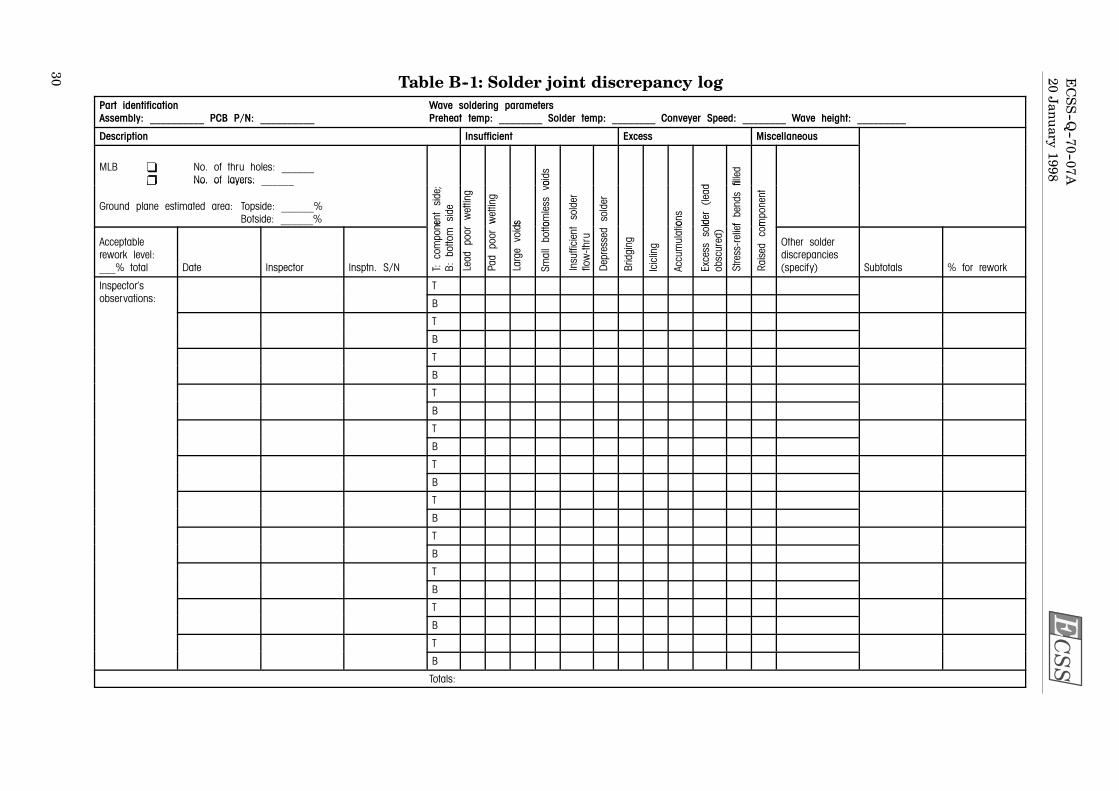
NOTE Deficient wave-soldered connections are caused most frequentlyby the movement of component leads during solidification, thepresence of solder alloywithin stress relief bendsand the entrap-ment of machine oils and solder fluxes within the solder fillet.Rework of any nature is costly. It involves not only the risk of ir-reparable lifted pads and measling, but also the possibility ofheat damage to sensitive components.
A solder-joint-discrepancy log, such as that given in annex B, shall bemaintainedas an aid to process control, optimisation of parameters and repeatability.
ECSS20 January 1998ECSS--Q--70--07A
16
(This page is intentionally left blank)
ECSS 20 January 1998
ECSS--Q--70--07A
17
5
Request for verification of process
5.1 GeneralVerification tests shall be conducted to establish confidence in the reliability of allautomatic machine soldering production lines.
Each application for verification shall contain a brief description of the facility,details of past experience and the name of the spacecraft project concerned; theapplication shall be signed by the person responsible forspace-component-assembly processes and addressed to the relevant finalcustomer�s Materials and Processes engineer responsible for that project.
5.2 DocumentationThe following documents shall also be forwarded with the application forevaluation:
a. company organigram related to wave-soldering production and controlpersonnel (including names and functions of all key personnel involved);
b. list of materials such as solder, flux, solvents, PCBs and equipment(including types and names of supplier) used for wave soldering;
c. production flow chart, showing quality assurance inspection points;
d. list of process specifications, including reference numbers of relevantin-house documents. The general process requirements shall include thoselisted in annex A;
e. detailed report concerning optimisation of wave-soldering processparameters (i.e. preheat temperature, temperature of solder, conveyer speed,temperature -- time profile, control of dross, cleaning procedure);
f. outline of company test capabilities (e.g. thermal cycling chambers,metallography, chemical analysis, failure analysis).
5.3 SamplesThe application shall be accompanied by three samples of wave-solder assembledboards whose complexity is typical of that found in spacecraft and which meetspace-quality workmanship standards. They shall have been cleaned, but notconformally coated. These items are hereinafter referred to as technologysamples.
ECSS20 January 1998ECSS--Q--70--07A
18
(This page is intentionally left blank)
ECSS 20 January 1998
ECSS--Q--70--07A
19
6
Technology samples
6.1 ConfigurationThe technology samples shall consist of PCBs procured from a space-approvedmanufacturing line, which shall be assembled with components to a documentedprocedure as detailed in annex A. A listing of these procedures shall form part ofthe line�s Process Identification Document (PID). Except for the actual machinesoldering procedure, the full component assembly requirements ofECSS--Q--70--08 shall apply. The assembled board shall be free of flux residuesand other contaminants.
6.2 Accompanying dataA description of the components, materials and processes utilised, together withthe cleanliness test report, shall accompany the technology samples.
The cleanliness tests shall be made by the contractor using a method the sameas, or equivalent to, requirements of ECSS--Q--70--08.
6.3 ExaminationThe technology samples shall be assessed by the final customer or by a recognisedtest house. Visual and metallographic inspections are required. Afterexamination, the completed report shall be sent to the supplier.
ECSS20 January 1998ECSS--Q--70--07A
20
(This page is intentionally left blank)
ECSS 20 January 1998
ECSS--Q--70--07A
21
7
Line audit
Provided the technology samples are found acceptable, the final customer shallaudit the wave-soldering and related facilities at a time when the equipment is inoperation. The audit shall also include a further on-site review of thedocumentation listed in subclauses 5.2 and 6.2. Compliance with the processrequirements of annex A shall be evaluated.
The final customer shall supply the manufacturer with a copy of the audit report.
ECSS20 January 1998ECSS--Q--70--07A
22
(This page is intentionally left blank)
ECSS 20 January 1998
ECSS--Q--70--07A
23
8
Verification
8.1 Planning, management and financeAfter the successful completion of the line audit, the supplier shall furnish thefinal customer with an evaluation programme and flow chart for approval, Theevaluation programme shall be performed by the supplier�s quality laboratoriesunder the supervision of a product assurance engineer, or by one or moreindependent test houses. Each test house shall require the final customer�sapproval prior to commencement of the programme. The entire evaluationprogramme shall be financed by the supplier and may be monitored by the finalcustomer at various stages during testing.
8.2 Description of samplesThe programme shall be designed to contain the following:
a. Five PCBs from each production line assembled according to thewave-soldering procedure of annex A. Each board shall have an identicallayout (i.e. dimensions, number of layers, type of components).
b. The layout and component density (i.e. number of components per unit boardarea) shall be similar to that envisaged for spacecraft circuits.
c. The variety of component packagesmounted on each board shall be restrictedto those envisaged for spacecraft circuits. There shall be at least three of eachtype per board. Particular attention shall be given to heat-sensitivecomponents. Only component types utilised during this programme shall beregarded as process approved.
NOTE Owing to the high cost of some components, the final customermay agree to the use of non-functional, or commercial-qualitycomponents but they shall be of the same leadmaterial and finish(viz. solderability) as the hi-rel components required for flight.
d. Each component type shall be tabulated, together with details concerning:
S component lead material and finish;
S lead diameter-to-hole diameter ratio.
ECSS20 January 1998ECSS--Q--70--07A
24
8.3 Initial testsa. The following initial tests shall be performed on each of the five assembled
PCBs:
S Visual inspection to ECSS--Q--70--08;
S Cleanliness test according to, or equivalent to, the method detailed inECSS--Q--70--08;
S Warp (bow) and twist of circuit board (see ECSS--Q--70--10), limits are:--
S Electrical continuity measurement for multilayer boards (not arequirement for double-sided PCBs); the circuit shall include at least 25%of all holes with at least one internal connection per hole (seeECSS--Q--70--10).
b. One printed circuit board is to be kept for reference.
8.4 Environmental exposurea. The four test samples shall be temperature cycled in air, 200 cycles from --55
°C (±5 °C) to +100 °C (±5 °C) at an average heating or cooling rate of 10 °C/min.The sample dwell time shall be 10 minutes ±5 minutes at each of thetemperature extremes.
b. Assembled PCBs are not required to be vibration tested unless the assembliesdeviate from the design requirements and workmanship standardsprescribed in ECSS--Q--70--08.
8.5 Final testsFollowing completion of exposure to 200 temperature cycles:
a. Each sample shall be visually inspected to ECSS--Q--70--08.
b. Multilayer boards shall be subjected to electrical continuity measurementswhich shall be monitored throughout a further 10 thermal cycles. Positivechanges greater than 5 % shall be cause for failure.
c. At least two components, of each available type, shall be microsectioned so asto dissect their component leads. Components selected for microsectioningshall be those having, from visual inspection results, the worst solder filletaspect. Evidence of propagating cracks in the solder joint vicinity shall because for failure, there shall be no defects in the board.
d. The leads of at least two components shall be cut and pull--tested at a constantstrain rate; the results shall be compared with the values obtained foridentical components on the reference board. Pull--testing shall be performedin a direction perpendicular (+5°) to the board surface. Fracture loads andpositions shall be recorded. A 25 % reduction of mechanical strength afterenvironmental testing shall be cause for failure.
8.6 Final reportThe supplier shall prepare a final report containing a description of the samples(subclause 5.2), where possible a photograph of an assembled board, and the fullresults of all tests performed to subclauses 5.3 and 5.5.
ECSS 20 January 1998
ECSS--Q--70--07A
25
9
Final customer approval
9.1 NotificationOn successful completion of the verification programme and the submittal of thereport to the final customer, the supplier shall receive a letter confirming that theverification programme has been approved.
9.2 Approval durationWhen there are no changes to the Process Identification Document (PID) theperiod of validity is indefinite and takes effect from the date onwhich the success-ful verification programme ended.
9.3 Renewal of final customer approvalA new verification test programme shall be carried out whenever a change to thePID has been proposed.
9.4 Withdrawal of final customer approvalThe final customer�s approval of any wave-soldering line shall be withdrawn inany of the following cases:
a. the supplier experiences rework activities of more than 5 %;
b. any of the materials, permitted component types or manufacturing processeshave been changed without prior authorisation (i.e. changes to the PID).
NOTE All modifications to the documents listed in subclauses 5.2 athrough 5.2 c shall require final customer approval before imple-mentation.
c. the final customer or his intermediate suppliers have experienced delays indelivery or manufacturing defects directly attributable to the wave-solderingprocess. Renewed approval may be granted following a review of thediscrepancy(ies). A repeat, or partial repeat of the verification programmemay be considered necessary.
ECSS20 January 1998ECSS--Q--70--07A
26
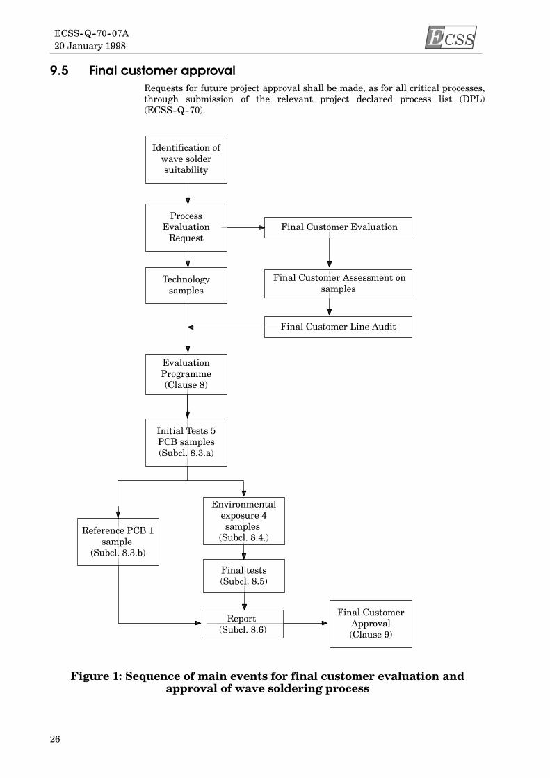
9.5 Final customer approvalRequests for future project approval shall be made, as for all critical processes,through submission of the relevant project declared process list (DPL)(ECSS--Q--70).
Final Customer Line Audit
Final Customer Assessment onsamples
Identification ofwave soldersuitability
Report(Subcl. 8.6)
Final Customer Evaluation
Final CustomerApproval(Clause 9)
Final tests(Subcl. 8.5)
Environmentalexposure 4samples
(Subcl. 8.4.)Reference PCB 1
sample(Subcl. 8.3.b)
Initial Tests 5PCB samples(Subcl. 8.3.a)
EvaluationProgramme(Clause 8)
Technologysamples
ProcessEvaluationRequest
Figure 1: Sequence of main events for final customer evaluation andapproval of wave soldering process
ECSS 20 January 1998
ECSS--Q--70--07A
27
Annex A (normative)
Process requirements for wave soldering of
printed-circuit boards
1. These requirements are applicable to all operations related to automaticmachine soldering.
2. Except when otherwise specified and approved by the final customer, allmaterials andprocessesutilised in soldering and cleaning operationsshallconform to ECSS--Q--70--08 and ECSS--Q--70--10.
3. Non-activated rosin fluxes are preferred, but mildly activated flux ispermitted (See ECSS--Q--70--08 for approved flux products). All fluxesshall be adjusted frequently (e.g. specific gravity) to avoid variations fromthe optimum. When mildly activated fluxes are used, they should bechanged frequently to ensure a constant and adequate level of activation.
NOTE All fluxes, machine oils and ionisable contaminants on the as-sembly shall be removed within one hour of the wave-solderingoperation.
4. The soldering area and machines shall be kept clean and orderly.Appropriate precautions shall be taken to avoid electrostatic-dischargeproblems as defined in ECSS--Q--70--08. Grounding of the conveyer is tobe envisaged. Toxic or volatile vapours shall be exhausted. Lightingfacilities and component lead preparations shall be as defined inECSS--Q--70--08. Deviations shall require final customer approval beforeimplementation.
5. Dross (oxides) shall be periodically removed fromthe solder bath to ensurethat dross does not mix with the liquid solder. Automatic or manualmethods are acceptable, provided that the dross does not come in contactwith the PCB assembly during any portion of the soldering process. Drossremoval materials shall not melt, dissolve or alloy with the liquid solderand flux.
6. Soldering equipment shall heat the PCB assemblies uniformly and havethe capacity to maintain the temperature during repetitive solderoperations with a maximum variation of +5 °C of the normal solderingtemperature.
ECSS20 January 1998ECSS--Q--70--07A
28
7. The supplier shall maintain operating procedures which describe thesoldering process and its associated equipment. For the solderingmachine, these procedures shall, as a minimum for given PCB assemblylayouts, define the controlled fluxing unit, preheat temperature, soldertemperature, rate of travel, cooling areas, frequency oftemperature-verification measurements, frequency of solder bathanalysis, masking and cleaning requirements. A listing of these processestogether with their issue numbers and dates of issue shall form part of thePID.
8. The assembled board shall not become contaminated before being loadedon the carrier.
9. The preheat temperature shall be controlled to avoid damage to the PCBand the component package.
10. The conveyer speed shall not vary by more than ±5 %.
11. The solder temperature shall be controlled so that the solder in the wavemaking contact with the board is 235--275 °C (see 6).
12. The height of the solderwave shall be controlled to a constant pre-selectedvalue across the width of the wave.
13. A machine-soldering logbook shall be maintained, showing theparameters required from requirements 9 -- 12 in order to repeatpreviously successful runs. The logbook shall also be used to documentresults of solder-bath analyses and results of the, cleanliness teststipulated in requirement 14.
14. Cleanliness checks according to the requirements of ECSS--Q--70--08 shallbe applied at established intervals, to pre-established resistivity limits.Intervals shall be based on the number and size of boards cleaned as wellas time.
15. Inspection criteria detailed in ECSS--Q--70--08 are applicable tomachine-solderedassemblies.Warpand twist of the boardshall notexceedthe limits specified by the detail drawing.
16. The rework of defective solder connections is permitted by hand soldering,provided this is not performed onmore than 5% of the solder connections.Any reworked boards shall be further cleaned and cleanliness tested andshall meet all the requirements of this Annex.
17. The leads of certain spacecraft components are designed for lap-solderingonto specially designed pads. They shall not be bent and subjected towavesoldering. Such components shall be manually assembled to the PCB in asubsequent operation and according to the requirements ofECSS--Q--70--08.
Note: The originator of the submission should complete items 4, 5, 6 and 7.This form is available as a Word and Wordperfect--Template on internet under