Spec. No ASP/DST1/E1-02 Rev. No 07 PURCHASE SPECIFICATION Department: ASSCP Unit : Corporate R & D Page 1 of 15 COPYRIGHT AND CONFIDENTIAL The information on this document is the property of Bharat Heavy Electricals Ltd. It must not be used directly or indirectly in anyway detrimental to the interest of the company ITEM: Multi Chamber Process Equipment for the deposition of amorphous silicon and Indium tin oxide layers for heterojunction solar cells S. No. TECHNICAL SPECIFICATION VENDOR’S CONFIRMATION 1. SCOPE AND FUNCTIONAL REQUIREMENTS A customized system is required to deposit doped and undoped amorphous silicon (a-Si:H) and indium tin oxide (ITO) films on either 9 pseudo-square silicon wafers of size 125 mm x 125 mm or 4 pseudo-square silicon wafers of size 156 mm x156 mm in a single run, to produce a stacked structure as shown in Figure 1. The wafer thickness will be around 200 micrometer. The system will integrate plasma enhanced chemical vapor deposition (PECVD) and sputtering chambers in an in- line configuration to deposit all the layers in the sequence given in Figure 2 without breaking the vacuum. The typical thickness value for an individual a-Si:H layer will be 5 -20 nanometer and that for ITO layer will be 50 - 200 nanometer. The system will have one load lock, one isolation chamber, three PECVD chambers for intrinsic, p-type and n-type amorphous silicon and one chamber for ITO deposition by sputtering in the sequence as shown in Figure 2. The wafer carrier will enter the system from load lock and exit from the same load lock after the deposition of desired layers from the corresponding chambers. The transport and deposition should be computer controlled and recipe driven with the option of partial or complete manual operation. Note: The schematics are just to guide design and should not be taken as a reason for compromising the functional requirements of the system. It is intended to shut off the pumping after daily operations and start it afresh for next operation without venting in between. The base pressure and the substrate heating requirements mentioned should be attainable within 5 hours of start up. APPROVED BY S. Bhattacharya CHECKED PREPARED DATE REVISION (07) S. P.Singh S. Chandril Annexure I
Transcript
Spec. No ASP/DST1/E1-02
Rev. No 07
PURCHASE SPECIFICATION
Department: ASSCP
Unit : Corporate R & D Page 1 of 15
CO
PY
RIG
HT
AN
D C
ON
FID
EN
TIA
L
Th
e in
form
atio
n o
n t
his
do
cum
ent
is t
he
pro
per
ty o
f B
har
at H
eavy
Ele
ctri
cals
Ltd
. It
mu
st n
ot
be
use
d d
irec
tly
or
ind
irec
tly
in a
nyw
ay d
etri
men
tal
to t
he
inte
rest
of
the
com
pan
y
ITEM: Multi Chamber Process Equipment for the deposition of amorphous silicon and Indium tin
oxide layers for heterojunction solar cells
S.
No.
TECHNICAL SPECIFICATION VENDOR’S
CONFIRMATION
1. SCOPE AND FUNCTIONAL REQUIREMENTS
A customized system is required to deposit doped and undoped amorphous silicon
(a-Si:H) and indium tin oxide (ITO) films on either 9 pseudo-square silicon wafers
of size 125 mm x 125 mm or 4 pseudo-square silicon wafers of size 156 mm x156
mm in a single run, to produce a stacked structure as shown in Figure 1. The wafer
thickness will be around 200 micrometer. The system will integrate plasma
enhanced chemical vapor deposition (PECVD) and sputtering chambers in an in-
line configuration to deposit all the layers in the sequence given in Figure 2
without breaking the vacuum. The typical thickness value for an individual a-Si:H
layer will be 5 -20 nanometer and that for ITO layer will be 50 - 200 nanometer.
The system will have one load lock, one isolation chamber, three PECVD chambers
for intrinsic, p-type and n-type amorphous silicon and one chamber for ITO
deposition by sputtering in the sequence as shown in Figure 2. The wafer carrier
will enter the system from load lock and exit from the same load lock after the
deposition of desired layers from the corresponding chambers. The transport and
deposition should be computer controlled and recipe driven with the option of
partial or complete manual operation.
Note: The schematics are just to guide design and should not be taken as a
reason for compromising the functional requirements of the system.
It is intended to shut off the pumping after daily operations and start it afresh for
next operation without venting in between. The base pressure and the substrate
heating requirements mentioned should be attainable within 5 hours of start up.
APPROVED BY
S. Bhattacharya
CHECKED PREPARED DATE
REVISION (07)
S. P.Singh S. Chandril
Annexure I
Spec. No ASP/DST1/E1-02
Rev. No 07
PURCHASE SPECIFICATION
Department: ASSCP
Unit : Corporate R & D Page 2 of 15
CO
PY
RIG
HT
AN
D C
ON
FID
EN
TIA
L
Th
e in
form
atio
n o
n t
his
do
cum
ent
is t
he
pro
per
ty o
f B
har
at H
eavy
Ele
ctri
cals
Ltd
. It
mu
st n
ot
be
use
d d
irec
tly
or
ind
irec
tly
in a
nyw
ay d
etri
men
tal
to t
he
inte
rest
of
the
com
pan
y
S.No TECHNICAL SPECIFICATION VENDOR’S
CONFIRMATION
1 SCOPE AND FUNCTIONAL REQUIREMENTS
The system and chamber dimensions should be optimally chosen to meet the
process requirements in the respective chambers in terms of the uniformity and
quality of the films. Special care should be taken in designing showerhead electrode,
heating arrangement, isolation gate valves to provide a contamination-free
environment in the process chambers. The vendor will provide all the items and
accessories to monitor and control the system as an independent unit. BHEL scope is
limited to furnishing the facility requirements such as power, water, compressed air,
abatement system etc. up to a common point on the support structure of system.
Process gases will also be provided by BHEL.
2 DETAILS OF EQUIPMENT
2A
Single run
capability
Processing of 9 pseudo-square silicon wafers of size 125 mm x 125
mm or 4 pseudo-square silicon wafers of size 156 mm x156 mm in a
single run
2B
System
configuration
1 entrance conveyor and 6 rectangular vacuum chambers
connected in In-line configuration. The vacuum chambers will be
fabricated from SS 304 and will have fixtures and ports for
mounting heaters, pumps, gauges, transport mechanism, power
supply connections, viewing ports etc. The chambers will be electro
polished from Inside and glass bead blasted from outside. Gate
valves must be installed at the start of load lock, between all
adjacent chambers and at the end of ITO chamber to perfectly
isolate the chamber process environment from the environment of
the adjacent chambers or atmosphere.
a. Speed Variable, up to 1000 mm/min. 2C
Wafer Carrier
Transport
properties
b. Capabilities
& operation
Smooth transfer of wafer carrier in both
directions and full integration with the system
automation.
Spec. No ASP/DST1/E1-02
Rev. No 07
PURCHASE SPECIFICATION
Department: ASSCP
Unit : Corporate R & D Page 3 of 15
CO
PY
RIG
HT
AN
D C
ON
FID
EN
TIA
L
Th
e in
form
atio
n o
n t
his
do
cum
ent
is t
he
pro
per
ty o
f B
har
at H
eavy
Ele
ctri
cals
Ltd
. It
mu
st n
ot
be
use
d d
irec
tly
or
ind
irec
tly
in a
nyw
ay d
etri
men
tal
to t
he
inte
rest
of
the
com
pan
y
S.
No. TECHNICAL SPECIFICATION
VENDOR’S
CONFIRMATION
2. DETAILS OF EQUIPMENT
i. Base
pressure
(Torr)
< 1 x 10⁻³
at 150 °C substrate
temperature
ii. Pumping Dry
iii. Substrate
Heating
~200 °C in 20 minutes using IR heaters
inside the chamber or heaters
mounted on the lid or bottom plate or
on both on the atmospheric side of
the chamber. The design of the
mounting of heaters should be such
that the viton gaskets mounted on the
flanges do not get damaged due to
heating.
a.
Load Lock
chamber
iv. View ports ≥ 2
i. Base
pressure
≤ 8 x 10⁻⁷
Torr at 150 °C temperature
after appropriate heating for 3-4
hours.
ii. Substrate
heating
350 °C in 5 minutes using Infrared
heating
iii. View ports ≥ 2
b.
Isolation
chamber
iv. Ports with
isolation
valves
≥ 2, at the back side (port size : 40 KF)
2 D
Ch
am
be
r ca
pa
bil
itie
s
c. Deposition
chambers
(Features
common to
intrinsic, p-
type, n-
type and
ITO
chambers)
i. Substrate
heating
Up to 325 °C during process gas flow.
The wafer temperature should be
controlled between 100 to 325 °C
within ± 5 °C. The heaters should be
mounted on the atmosphere side of
the chamber. The design of the
mounting arrangement of heaters
should be such that the viton O-rings
mounted on the flanges do not get
damaged due to heating. Also
chamber should not develop any cold
regions in the chamber due to heater
design.
Spec. No ASP/DST1/E1-02
Rev. No 07
PURCHASE SPECIFICATION
Department: ASSCP
Unit : Corporate R & D Page 4 of 15
CO
PY
RIG
HT
AN
D C
ON
FID
EN
TIA
L
Th
e in
form
atio
n o
n t
his
do
cum
ent
is t
he
pro
per
ty o
f B
har
at H
eavy
Ele
ctri
cals
Ltd
. It
mu
st n
ot
be
use
d d
irec
tly
or
ind
irec
tly
in a
nyw
ay d
etri
men
tal
to t
he
inte
rest
of
the
com
pan
y
S.
No. TECHNICAL SPECIFICATION
VENDOR’S
CONFIRMATION
2. DETAILS OF EQUIPMENT
ii. Base
pressure
≤ 8 x 10⁻⁷
Torr at 150 °C substrate
temperature
PECVD Automatic control of
pressure in the range of 0.1
– 2 Torr
iii. Process
Pumping
ITO Automatic control of
pressure in the range of
10--4
– 10-2
Torr
iv. Process gas
flow
precision
± 1 sccm
PECVD ± 1 mTorr v. Process
pressure
precision
ITO ± 0.1 mTorr
Deposition
chambers
(Features
common to
intrinsic, p-
type, n-type
and ITO
chambers)
vi. Ports with
isolation
valves
≥ 2, at the back side (port size : 40 KF)
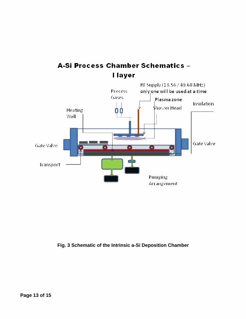
i. Mode of
deposition
Moving mode deposition with wafer
carrier travelling under the electrode
with gate valves closed on both sides
of the chamber
2 D
Ch
am
be
r ca
pa
bil
itie
s
c.
1. intrinsic
a-Si:H
ii. Plasma
sources
13.56 MHz (RF) and 40.68 MHz (VHF)
generators with automatic matching
network, both feeding power to the
same electrode(s). Only one source
to be used at a time. Power of the
generator should be up to 600 W.
Spec. No ASP/DST1/E1-02
Rev. No 07
PURCHASE SPECIFICATION
Department: ASSCP
Unit : Corporate R & D Page 5 of 15
CO
PY
RIG
HT
AN
D C
ON
FID
EN
TIA
L
Th
e in
form
atio
n o
n t
his
do
cum
ent
is t
he
pro
per
ty o
f B
har
at H
eavy
Ele
ctri
cals
Ltd
. It
mu
st n
ot
be
use
d d
irec
tly
or
ind
irec
tly
in a
nyw
ay d
etri
men
tal
to t
he
inte
rest
of
the
com
pan
y
Sl.
No. TECHNICAL SPECIFICATION
VENDOR’S
CONFIRMATION
2 DETAILS OF EQUIPMENT
Type Shower head electrode with dark space
shield, compatible with both RF and VHF
plasma generators
Size
(mm)
Length ~200, width – suitable for
uniform deposition on all wafers
iii. Electrode
Spacing
(mm)
10 – 40, adjustable after opening the
system
1 H2 & 1 SiH4 with required flow rates for typical
intrinsic a-Si:H deposition
1 for NF3 (0-500 sccm)
iv. MFCs on
gas
manifold
1 additional for SiH4 (0-100 sccm)
v. Process
pumping
Dry
vi. Resident
zones
On both sides of the electrode for parking wafer
carrier outside the plasma region
1.
Intr
insi
c a
-Si:
H
vii. View
port
3
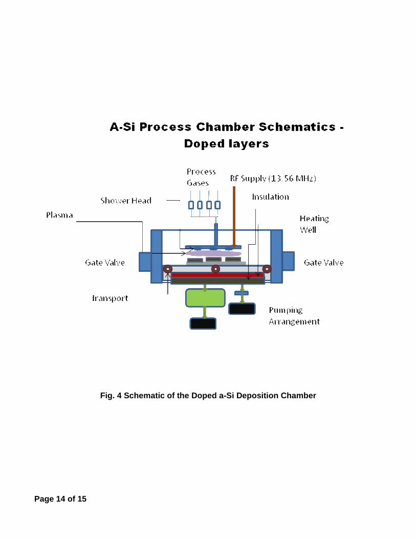
i. Mode of
depositio
n
Stationary mode deposition with wafer carrier
under the electrode
ii. Electrode Showerhead with dark space shield
2D
Ch
am
be
r ca
pa
bil
itie
s
c.
De
po
siti
on
ch
am
be
rs
2.
p-t
yp
e a
-Si:
H
iii. Plasma
source
13.56 MHz with 600 W capability
Spec. No ASP/DST1/E1-02
Rev. No 07
PURCHASE SPECIFICATION
Department: ASSCP
Unit : Corporate R & D Page 6 of 15
CO
PY
RIG
HT
AN
D C
ON
FID
EN
TIA
L
Th
e in
form
atio
n o
n t
his
do
cum
ent
is t
he
pro
per
ty o
f B
har
at H
eavy
Ele
ctri
cals
Ltd
. It
mu
st n
ot
be
use
d d
irec
tly
or
ind
irec
tly
in a
nyw
ay d
etri
men
tal
to t
he
inte
rest
of
the
com
pan
y
Sl.
No. TECHNICAL SPECIFICATION
VENDOR’S
CONFIRMATION
2 DETAILS OF EQUIPMENT
1 H2, 1 SiH4, 1 TMB, 1 B2H6 with required flow
rates for typical p-type a-Si:H deposition
1 for NF3 (0-100 sccm)
iv. MFCs on
gas
manifold
1 for SiH4 (0-100 sccm)
2.
p-t
yp
e a
-Si:
H
v. View
ports
2
i. Mode of
deposition
Stationary mode deposition with wafer carrier
under the electrode
ii. Electrode Showerhead with dark space shield
iii. Plasma
source
13.56 MHz with 600 W capability
1 H2, 2 SiH4 with required flow rates for typical n-
type a-Si:H deposition
1 for NF3 (0-100 sccm)
iv. MFCs on
gas
manifold
1 for SiH4 (0-100 sccm)
3.
n-t
yp
e a
-Si:
H
v. View
ports
2
i. Mode of
deposition
Moving mode deposition from top and bottom at
the same time with gate valves closed on both sides