Spec No. TQ3C-8EAF0-E1YAL22-00 S SPEC Date December 10, 2014 T TYPE : TCG121XGLPBPNN-AN40 < 12.1 inch XGA transmissive color TFT with LED backlight and constant current circuit for LED backlight> KYOCERA DISPLAY CORPORATION This specification is subject to change without notice. Consult Kyocera before ordering. Original Issue Date Designed by: Engineering dept. Confirmed by: QA dept. Prepared Checked Approved Checked Approved December 10, 2014 CONTENTS 1. Application 2. Construction and outline 3. Mechanical specifications 4. Absolute maximum ratings 5. Electrical characteristics 6. Optical characteristics 7. Interface signals 8. Input timing characteristics 9. Lot number identification 10. Warranty 11. Precautions for use 12. Reliability test data 13. Outline drawing Dec 19, 2014
Transcript
Spec No. TQ3C-8EAF0-E1YAL22-00 SSPEC Date December 10, 2014
TTYPE : TCG121XGLPBPNN-AN40 < 12.1 inch XGA transmissive color TFT with LED backlight
and constant current circuit for LED backlight>
KYOCERA DISPLAY CORPORATION
This specification is subject to change without notice. Consult Kyocera before ordering.
CONTENTS 1. Application 2. Construction and outline 3. Mechanical specifications 4. Absolute maximum ratings 5. Electrical characteristics 6. Optical characteristics 7. Interface signals 8. Input timing characteristics 9. Lot number identification
10. Warranty 11. Precautions for use 12. Reliability test data 13. Outline drawing
Dec 19, 2014
Spec No.
TQ3C-8EAF0-E1YAL22-00 Part No.
TCG121XGLPBPNN-AN40 Page
-
WWarning
1. This Kyocera LCD module has been specifically designed for use only in electronic devices and industrial machines in the area of audio control, office automation, industrial control, home appliances, etc. The module should not be used in applications where the highest level of safety and reliability are required and module failure or malfunction of such module results in physical harm or loss of life, as well as enormous damage or loss. Such fields of applications include, without limitation, medical, aerospace, communications infrastructure, atomic energy control. Kyocera expressly disclaims any and all liability resulting in any way to the use of the module in such applications.
2. Customer agrees to indemnify, defend and hold Kyocera harmless from and against any and all actions, claims, damages, liabilities, awards, costs, and expenses, including legal expenses, resulting from or arising out of Customer's use, or sale for use, or Kyocera modules in applications.
Caution
1. Kyocera shall have the right, which Customer hereby acknowledges, to immediately scrap or destroy tooling for Kyocera modules for which no Purchase Orders have been received from the Customer in a two-year period.
Spec No.
TQ3C-8EAF0-E1YAL22-00 Part No.
TCG121XGLPBPNN-AN40 Page
-
Revision record
Date Designed by : Engineering dept. Confirmed by : QA dept.
Prepared Checked Approved Checked Approved
Rev.No. Date Page Descriptions
Spec No.
TQ3C-8EAF0-E1YAL22-00 Part No.
TCG121XGLPBPNN-AN40 Page
1
1. Application
This document defines the specification of TCG121XGLPBPNN-AN40. (RoHS Compliant) 2. Construction and outline
LCD Backlight system Polarizer Interface Additional circuit
: Transmissive color dot matrix type TFT : LED : Anti-Glare treatment : LVDS : Timing controller, Power supply (3.3V input) With constant current circuit for LED Backlight(12V input)
3. Mechanical specifications
Item Specification Unit
Outline dimensions 1) 260.5(W)×203(H)×10.4(D) mm
Active area 245.76(W)×184.32(H) (30.8cm/12.1 inch(Diagonal)) mm
Dot format 1,024×(B,G,R)(W)×768(H) dot
Dot pitch 0.08(W)×0.24(H) mm
Base color 2) Normally Black -
Mass 555 g
1) Projection not included. Please refer to outline for details. 2) Due to the characteristics of the LCD material, the color varies with environmental temperature.
M407011
Spec No.
TQ3C-8EAF0-E1YAL22-00 Part No.
TCG121XGLPBPNN-AN40 Page
2
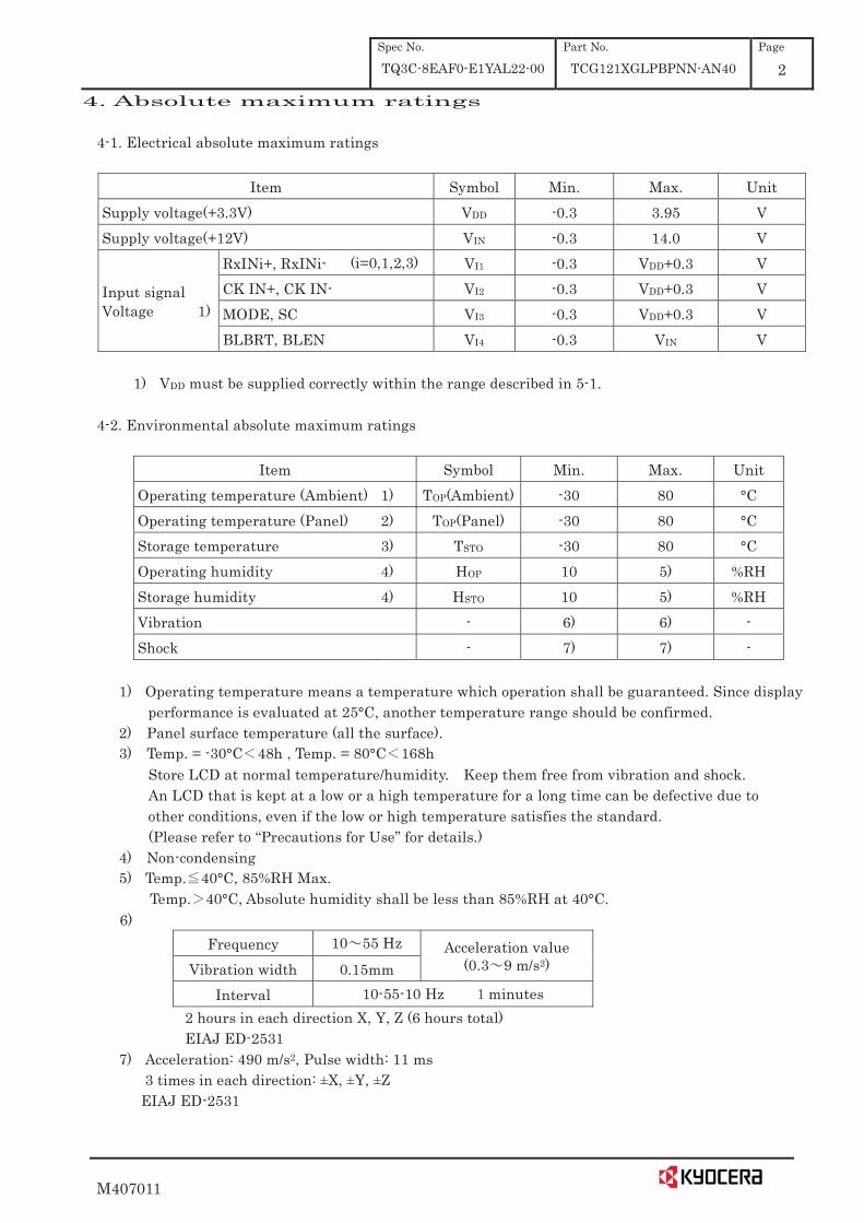
4. Absolute maximum ratings
4-1. Electrical absolute maximum ratings
Item Symbol Min. Max. Unit Supply voltage(+3.3V) VDD -0.3 3.95 V Supply voltage(+12V) VIN -0.3 14.0 V
Input signal Voltage 1)
RxINi+, RxINi- (i=0,1,2,3) VI1 -0.3 VDD+0.3 V CK IN+, CK IN- VI2 -0.3 VDD+0.3 V MODE, SC VI3 -0.3 VDD+0.3 V BLBRT, BLEN VI4 -0.3 VIN V
1) VDD must be supplied correctly within the range described in 5-1.
4-2. Environmental absolute maximum ratings
Item Symbol Min. Max. Unit
Operating temperature (Ambient) 1) TOP(Ambient) -30 80 °C Operating temperature (Panel) 2) TOP(Panel) -30 80 °C Storage temperature 3) TSTO -30 80 °C Operating humidity 4) HOP 10 5) %RH Storage humidity 4) HSTO 10 5) %RH Vibration - 6) 6) - Shock - 7) 7) -
1) Operating temperature means a temperature which operation shall be guaranteed. Since display
performance is evaluated at 25°C, another temperature range should be confirmed. 2) Panel surface temperature (all the surface).
3) Temp. = -30°C 48h , Temp. = 80°C 168h Store LCD at normal temperature/humidity. Keep them free from vibration and shock.
An LCD that is kept at a low or a high temperature for a long time can be defective due to other conditions, even if the low or high temperature satisfies the standard. (Please refer to “Precautions for Use” for details.)
4) Non-condensing 5) Temp. 40°C, 85%RH Max.
Temp. 40°C, Absolute humidity shall be less than 85%RH at 40°C. 6)
Frequency 10 55 Hz Acceleration value (0.3 9 m/s2) Vibration width 0.15mm
Interval 10-55-10 Hz minutes 2 hours in each direction X, Y, Z (6 hours total) EIAJ ED-2531
7) Acceleration: 490 m/s2, Pulse width: 11 ms 3 times in each direction: ±X, ±Y, ±Z
EIAJ ED-2531
M407011
Spec No.
TQ3C-8EAF0-E1YAL22-00 Part No.
TCG121XGLPBPNN-AN40 Page
3
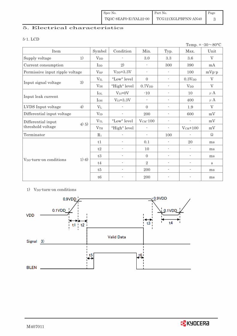
5. Electrical characteristics 5-1. LCD
Temp. = -30 80°C Item Symbol Condition Min. Typ. Max. Unit
Supply voltage 1) VDD - 3.0 3.3 3.6 V Current consumption IDD 2) - 300 390 mA Permissive input ripple voltage VRP VDD=3.3V - - 100 mVp-p
Input signal voltage 3) VIL "Low" level 0 - 0.3VDD V VIH "High" level 0.7VDD - VDD V
Input leak current IOL VI3=0V -10 - 10 A
IOH VI3=3.3V - - 400 A LVDS Input voltage 4) VL - 0 - 1.9 V Differential input voltage VID - 200 - 600 mV
5) VCM : LVDS Common mode voltage (VCM=1.25V 6) Please power on LVDS transmitter at the same time as VDD, or LVDS transmitter should be
powered on first.
M407011
Spec No.
TQ3C-8EAF0-E1YAL22-00 Part No.
TCG121XGLPBPNN-AN40 Page
5
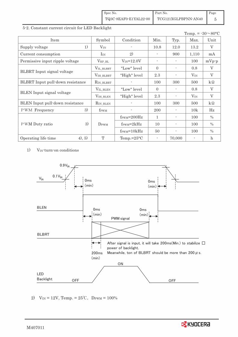
5-2. Constant current circuit for LED Backlight Temp. = -30 80°C
Item Symbol Condition Min. Typ. Max. Unit Supply voltage 1) VIN - 10.8 12.0 13.2 V Current consumption IIN 2) - 900 1,110 mA Permissive input ripple voltage VRP_BL VIN=12.0V - - 100 mVp-p
BLBRT Input signal voltage VIL_BLBRT "Low" level 0 - 0.8 V VIH_BLBRT "High" level 2.3 - VIN V
BLBRT Input pull-down resistance RIN_BLBRT - 100 300 500 k
BLEN Input signal voltage VIL_BLEN "Low" level 0 - 0.8 V VIH_BLEN "High" level 2.3 - VIN V
BLEN Input pull-down resistance RIN_BLEN - 100 300 500 k Frequency 3) fPWM - 200 - 10k Hz
M Duty ratio 3) DPWM fPWM=200Hz 1 - 100 % fPWM=2kHz 10 - 100 %
fPWM=10kHz 50 - 100 % Operating life time 4), 5) T Temp.=25°C - 70,000 - h
1) VIN-turn-on conditions
2) VIN = 12V, Temp. = 25 DPWM = 100%
M407011
Spec No.
TQ3C-8EAF0-E1YAL22-00 Part No.
TCG121XGLPBPNN-AN40 Page
6
3) Timing Diagram
tON tOFF 50 s. In case of lower frequency, the deterioration of the display quality, flicker etc., may occur.
4) When brightness decrease 50% of minimum brightness.
The average life of a LED will decrease when the LCD is operating at higher temperatures.
5) Life time is estimated data.(Condition : IF=(75)mA, Ta=25 in chamber).
M407011
Spec No.
TQ3C-8EAF0-E1YAL22-00 Part No.
TCG121XGLPBPNN-AN40 Page
7
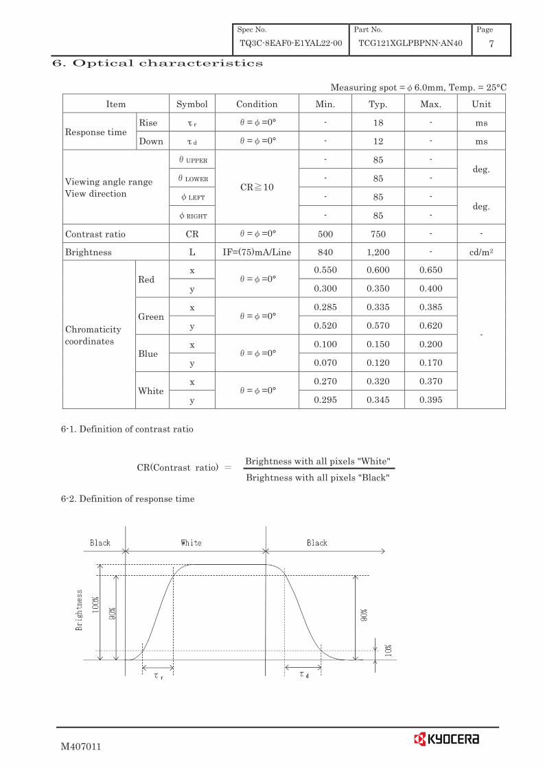
6. Optical characteristics
Measuring spot = 6.0mm, Temp. = 25°C
Item Symbol Condition Min. Typ. Max. Unit
Response time Rise r = =0° - 18 - ms
Down d = =0° - 12 - ms
Viewing angle range View direction
UPPER
CR 10
- 85 - deg.
LOWER - 85 -
LEFT - 85 - deg.
RIGHT - 85 -
Contrast ratio CR = =0° 500 750 - -
Brightness L IF=(75)mA/Line 840 1,200 - cd/m2
Chromaticity coordinates
Red x
= =0° 0.550 0.600 0.650
-
y 0.300 0.350 0.400
Green x
= =0° 0.285 0.335 0.385
y 0.520 0.570 0.620
Blue x
= =0° 0.100 0.150 0.200
y 0.070 0.120 0.170
White x
= =0° 0.270 0.320 0.370
y 0.295 0.345 0.395
6-1. Definition of contrast ratio
CR(Contrast ratio)
Brightness with all pixels "White"
Brightness with all pixels "Black"
6-2. Definition of response time
M407011
Spec No.
TQ3C-8EAF0-E1YAL22-00 Part No.
TCG121XGLPBPNN-AN40 Page
8
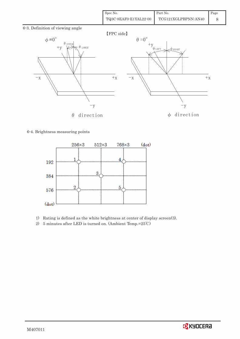
6-3. Definition of viewing angle FPC side
6-4. Brightness measuring points
1) Rating is defined as the white brightness at center of display screen(3). 2) 5 minutes after LED is turned on. (Ambient Temp.=25 )
M407011
Spec No.
TQ3C-8EAF0-E1YAL22-00 Part No.
TCG121XGLPBPNN-AN40 Page
9
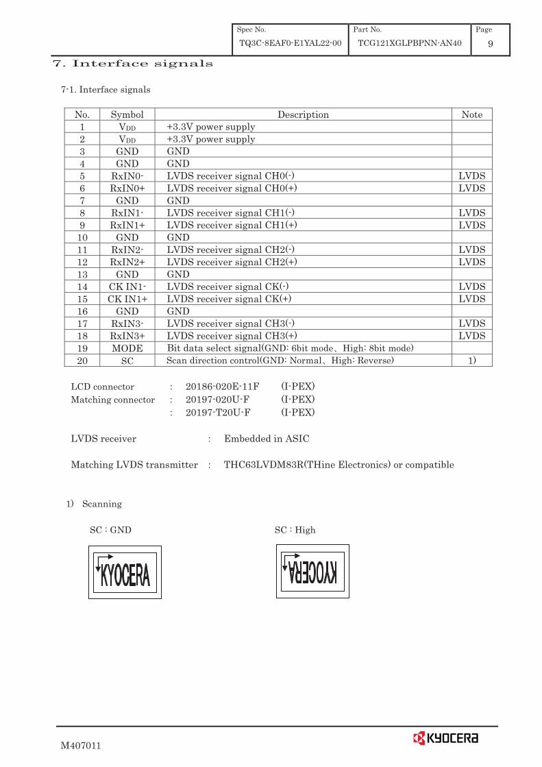
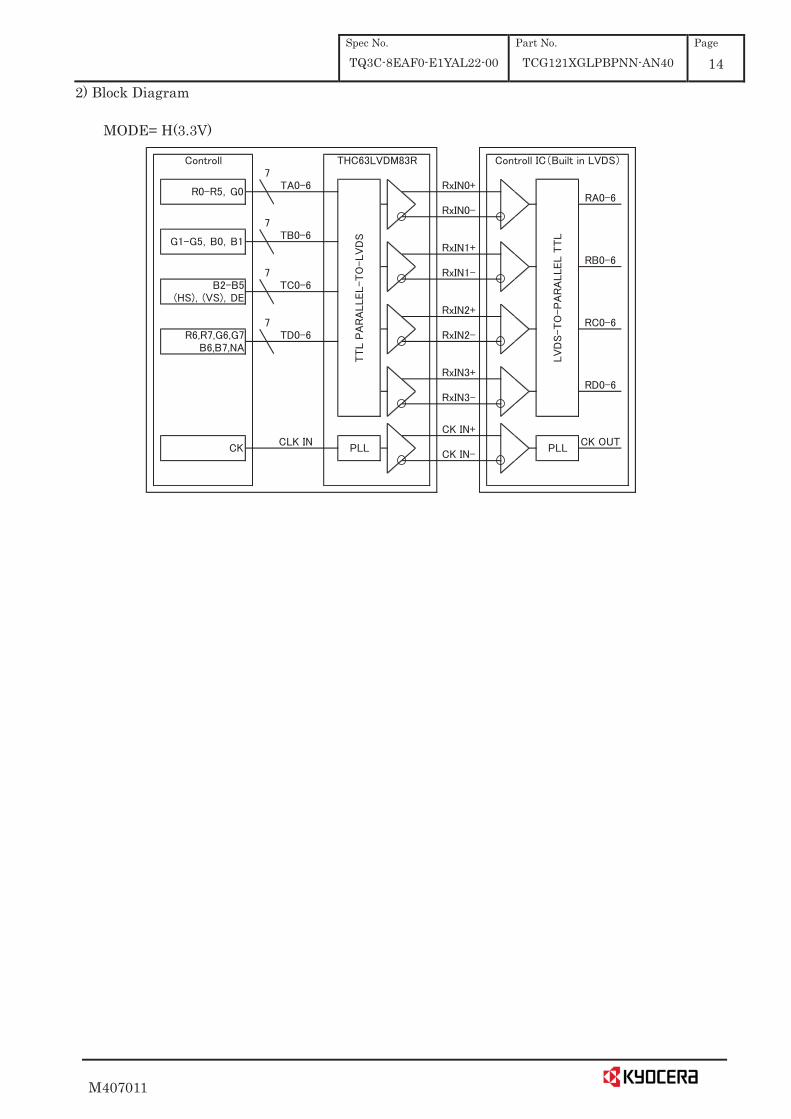
7. Interface signals
7-1. Interface signals
No. Symbol Description Note 1 VDD +3.3V power supply 2 VDD +3.3V power supply 3 GND GND 4 GND GND 5 RxIN0- LVDS receiver signal CH0(-) LVDS 6 RxIN0+ LVDS receiver signal CH0(+) LVDS 7 GND GND 8 RxIN1- LVDS receiver signal CH1(-) LVDS 9 RxIN1+ LVDS receiver signal CH1(+) LVDS 10 GND GND 11 RxIN2- LVDS receiver signal CH2(-) LVDS 12 RxIN2+ LVDS receiver signal CH2(+) LVDS 13 GND GND 14 CK IN1- LVDS receiver signal CK(-) LVDS 15 CK IN1+ LVDS receiver signal CK(+) LVDS 16 GND GND 17 RxIN3- LVDS receiver signal CH3(-) LVDS 18 RxIN3+ LVDS receiver signal CH3(+) LVDS 19 MODE Bit data select signal(GND: 6bit mode High: 8bit mode) 20 SC Scan direction control(GND: Normal High: Reverse) 1)
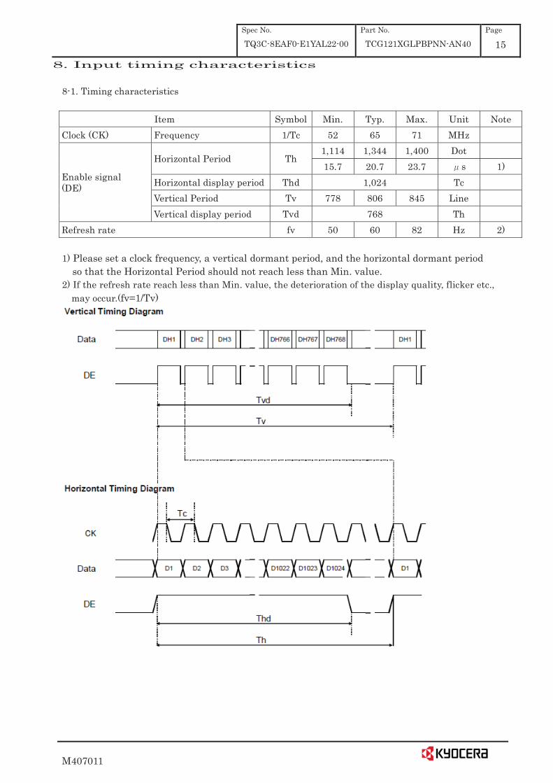
Item Symbol Min. Typ. Max. Unit Note Clock (CK) Frequency 1/Tc 52 65 71 MHz
Enable signal (DE)
Horizontal Period Th 1,114 1,344 1,400 Dot 15.7 20.7 23.7 s 1)
Horizontal display period Thd 1,024 Tc Vertical Period Tv 778 806 845 Line Vertical display period Tvd 768 Th
Refresh rate fv 50 60 82 Hz 2)
1) Please set a clock frequency, a vertical dormant period, and the horizontal dormant period so that the Horizontal Period should not reach less than Min. value.
2) If the refresh rate reach less than Min. value, the deterioration of the display quality, flicker etc., may occur.(fv=1/Tv)
M407011
Spec No.
TQ3C-8EAF0-E1YAL22-00 Part No.
TCG121XGLPBPNN-AN40 Page
16
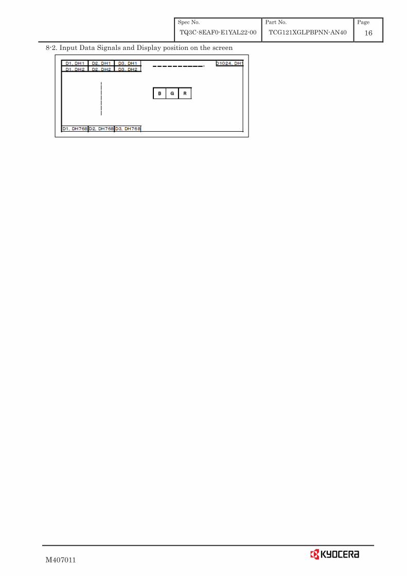
8-2. Input Data Signals and Display position on the screen
M407011
Spec No.
TQ3C-8EAF0-E1YAL22-00 Part No.
TCG121XGLPBPNN-AN40 Page
17
9. Lot number identification
The lot number shall be indicated on the back of the backlight case of each LCD.
TCG121XGLPBPNN-AN40 - - - MADE IN
1 2 3 4 5
Year 2014 2015 2016 2017 2018 2019
Code 4 5 6 7 8 9
Month Jan. Feb. Mar. Apr. May Jun.
Code 1 2 3 4 5 6
Month Jul. Aug. Sep. Oct. Nov. Dec.
Code 7 8 9 X Y Z 10. Warranty
10-1. Incoming inspection
Please inspect the LCD within one month after your receipt. 10-2. Production warranty
Kyocera warrants its LCD’s for a period of 12 months from the ship date. Kyocera shall, by mutual agreement, replace or re-work defective LCD’s that are shown to be Kyocera’s responsibility.
No1. - No5. above indicate 1. Year code 2. Month code 3. Date 4. Version Number 5. Country of origin (Japan or China)
M407011
Spec No.
TQ3C-8EAF0-E1YAL22-00 Part No.
TCG121XGLPBPNN-AN40 Page
18
11. Precautions for use
11-1. Installation of the LCD 1) A transparent protection plate shall be added to protect the LCD and its polarizer. 2) The LCD shall be installed so that there is no pressure on the LSI chips. 3) Since this product is wide viewing product, occurrence level of in-plane unevenness by the external
stress is different compared to current normal viewing product. So there is a possibility that in-plane unevenness will be occurred by over twist, strain giving by attaching to LCD, and over pressure to touch panel. Please be careful of stress when designing the housing.
4) A transparent protection sheet is attached to the polarizer. Please remove the protection film slowly before use, paying attention to static electricity.
11-2. Static electricity 1) Since CMOS ICs are mounted directly onto the LCD glass, protection from static electricity is
required. 2) Workers should use body grounding. Operator should wear ground straps.
11-3. LCD operation 1) The LCD shall be operated within the limits specified. Operation at values outside of these limits
may shorten life, and/or harm display images. 2) Please select the best display pattern based on your evaluation because flicker, lines or
nonuniformity or unevenness can be visible depending on display patterns.
11-4. Storage 1) The LCD shall be stored within the temperature and humidity limits specified.
Store in a dark area, and protect the LCD from direct sunlight or fluorescent light. 2) Always store the LCD so that it is free from external pressure onto it.
11-5. Usage 1) DO NOT store in a high humidity environment for extended periods. Polarizer degradation bubbles,
and/or peeling off of the polarizer may result. 2) The front polarizer is easily scratched or damaged. Prevent touching it with any hard material, and
from being pushed or rubbed. 3) The LCD screen may be cleaned by wiping the screen surface with a soft cloth or cotton pad using a
little Ethanol. 4) Water may cause damage or discoloration of the polarizer. Clean condensation or moisture from
any source immediately. 5) Always keep the LCD free from condensation during testing. Condensation may permanently spot
or stain the polarizer. 6) Do not disassemble LCD because it will result in damage. 7) This Kyocera LCD has been specifically designed for use in general electronic devices, but not
for use in a special environment such as usage in an active gas. Hence, when the LCD is supposed to be used in a special environment, evaluate the LCD thoroughly beforehand and do not expose the LCD to chemicals such as an active gas.
8) Please do not use solid-base image pattern for long hours because a temporary afterimage may appear. We recommend using screen saver etc. in cases where a solid-base image pattern must be used.
9) Liquid crystal may leak when the LCD is broken. Be careful not to let the fluid go into your eyes and mouth. In the case the fluid touches your body; rinse it off right away with water and soap.
M407011
Spec No.
TQ3C-8EAF0-E1YAL22-00 Part No.
TCG121XGLPBPNN-AN40 Page
19
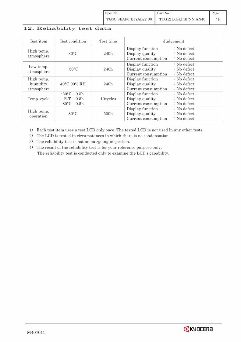
12. Reliability test data
Test item Test condition Test time Judgement
High temp. atmosphere 80°C 240h
Display function Display quality Current consumption
: No defect : No defect : No defect
Low temp. atmosphere -30°C 240h
Display function Display quality Current consumption
: No defect : No defect : No defect
High temp. humidity
atmosphere 40°C 90% RH 240h
Display function Display quality Current consumption
: No defect : No defect : No defect
Temp. cycle -30°C
R.T. 80°C
0.5h 0.5h 0.5h
10cycles Display function Display quality Current consumption
: No defect : No defect : No defect
High temp. operation 80°C 500h
Display function Display quality Current consumption
: No defect : No defect : No defect
1) Each test item uses a test LCD only once. The tested LCD is not used in any other tests. 2) The LCD is tested in circumstances in which there is no condensation. 3) The reliability test is not an out-going inspection. 4) The result of the reliability test is for your reference purpose only.
The reliability test is conducted only to examine the LCD's capability.
M407011
Spec No. TQ3C-8EAF0-E2YAL22-00 Date December 10, 2014
KKYOCERA INSPECTION STANDARD
TYPE : TCG121XGLPBPNN-AN40 KYOCERA DISPALY CORPORATION
Original Issue Date
Designed by : Engineering dept. Confirmed by : QA dept. Prepared Checked Approved Checked Approved
December 10, 2014
Spec No.
TQ3C-8EAF0-E2YAL22-00 Part No.
TCG121XGLPBPNN-AN40 Page
-
Revision record
Date Designed by : Engineering dept. Confirmed by : QA dept.
Prepared Checked Approved Checked Approved
Rev.No. Date Page Descriptions
Spec No.
TQ3C-8EAF0-E2YAL22-00 Part No.
TCG121XGLPBPNN-AN40 Page
1
Visuals specification 1) Note
Note General 1. Customer identified anomalies not defined within this inspection standard shall be
reviewed by Kyocera, and an additional standard shall be determined by mutual consent. 2. This inspection standard about the image quality shall be applied to any defect within the
effective viewing area and shall not be applicable to outside of the area.
3. Inspection conditions Luminance Inspection distance Temperature Direction
: 500 Lux min. : 300 mm. : 25 5 : Directly above
Definition of inspection item
Dot defect Bright dot defect The dot is constantly “on” when power applied to the LCD, even when all “Black” data sent to the screen. Inspection tool: 5% Transparency neutral density filter. Count dot: If the dot is visible through the filter. Don’t count dot: If the dot is not visible through the
filter.
Black dot defect
The dot is constantly “off” when power applied to the LCD, even when all “White” data sent to the screen. Similar size compared to bright dot.
White dot (Circular/foreign particle)
Pixel works electrically, however, circular/foreign particle makes dot appear to be “on” even when all “Black” data is sent to the screen.
Adjacent dot Adjacent dot defect is defined as two or more bright dot defects or black dot defects.