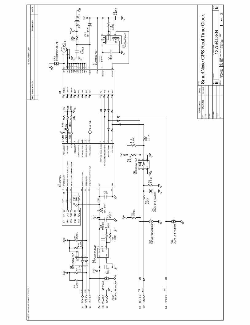
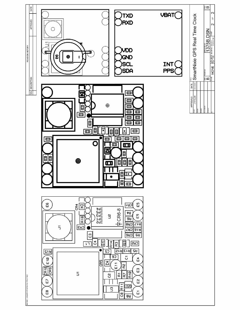
Taylor Electronics Services www.tayloredge.com C 2012 Specifications: 1375/1455 GPS RTC Rev: B Description: The 1375/1455 series modules are complete real time clocks (RTC) that use GPS data and a user supplied local time offset to replicate the register set of the NXP PCF8563 IC so that they can function as drop in replacements for the 1374/1362 RTC modules from TES. Additionally, the full GPS data from the GPGGA, GPGSA, GPGSV and GPRMC NMEA sentences is decoded on the fly to populate a 128 byte I 2 C register map with full navigational data. The PPS output is accurate to +/-1ppm. The RTC data interface is a standard I 2 C bus operating at 100kbps. The RTC/Slave side of the interface operates at an internal 3.3V regulated from the master side (VDD) input voltage from 3.3V to 5.5V. The master to slave I 2 C interface is level shifted and includes master side bus pull up resistors of 2.21K. All inputs and outputs are ESD protected (See notes on Table 2). Slave addressing information can be found in Fig. 8 and 9. The local time offset from UTC can be entered directly into the offset registers or can be set indirectly via a time setting function, such as is used in the TES SmartNixie clock backplane. The offset can be plus or minus 23h 59m 59s in 1s increments from UTC. A one hour positive offset function for DST is also included. Local time is computed from the GPS UTC and UDC data at the end of every second and includes date adjustments for leap years. DST can be turned on and off with a short clock set sequence or programmed directly as part of the local time offset.. Once a GPS fix has been established, the battery backed internal RTC will keep time for up to three months with +/-20ppm accuracy with the power off or no GPS fix. Satellite data is stored in battery backed RAM to speed fix acquisition after brief power or satellite view interruptions. An interrupt output (INT) can be set to pulse high for 560mS every second (1PPS), 30 seconds (1PP30S), minute (1PPM), hour (1PPH) or off, The INT goes high after the GPS data has been fully decoded and the local time calculation has been completed (Useful to control slave clocks). INT is low during NMEA sentence reception and then high during RS232 idle. Three lamps indicate the status of the module: FIX blinks at 10Hz when the GPS indicates no fix is available, 2Hz if the fix signal is toggling faster than once per two seconds and solid on when a stable fix is indicated. PPS blinks at 1Hz 50% duty when the GPS PPS is stable at 1Hz 10% duty. MON blinks at 5Hz all the time and signals the main processing loop is running. Fig 1. 1375 horizontal GPS RTC
Transcript
Taylor Electronics Services www.tayloredge.com C 2012
Specifications: 1375/1455 GPS RTC Rev: B
Description:
The 1375/1455 series modules are complete real time clocks (RTC) that use GPS data and a usersupplied local time offset to replicate the register set of the NXP PCF8563 IC so that they can functionas drop in replacements for the 1374/1362 RTC modules from TES. Additionally, the full GPS datafrom the GPGGA, GPGSA, GPGSV and GPRMC NMEA sentences is decoded on the fly to populate a128 byte I2C register map with full navigational data. The PPS output is accurate to +/-1ppm.
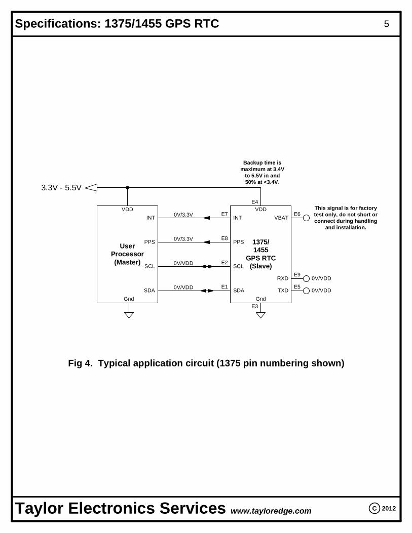
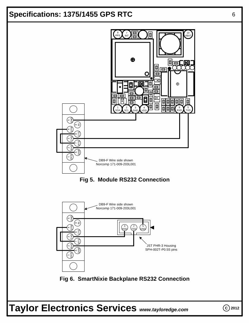
The RTC data interface is a standard I2C bus operating at 100kbps. The RTC/Slave side of theinterface operates at an internal 3.3V regulated from the master side (VDD) input voltage from 3.3V to5.5V. The master to slave I2C interface is level shifted and includes master side bus pull up resistors of2.21K. All inputs and outputs are ESD protected (See notes on Table 2). Slave addressing informationcan be found in Fig. 8 and 9.
The local time offset from UTC can be entered directly into the offset registers or can be setindirectly via a time setting function, such as is used in the TES SmartNixie clock backplane. The offsetcan be plus or minus 23h 59m 59s in 1s increments from UTC. A one hour positive offset function forDST is also included. Local time is computed from the GPS UTC and UDC data at the end of everysecond and includes date adjustments for leap years. DST can be turned on and off with a short clockset sequence or programmed directly as part of the local time offset..
Once a GPS fix has been established, the battery backed internal RTC will keep time for up tothree months with +/-20ppm accuracy with the power off or no GPS fix. Satellite data is stored inbattery backed RAM to speed fix acquisition after brief power or satellite view interruptions.
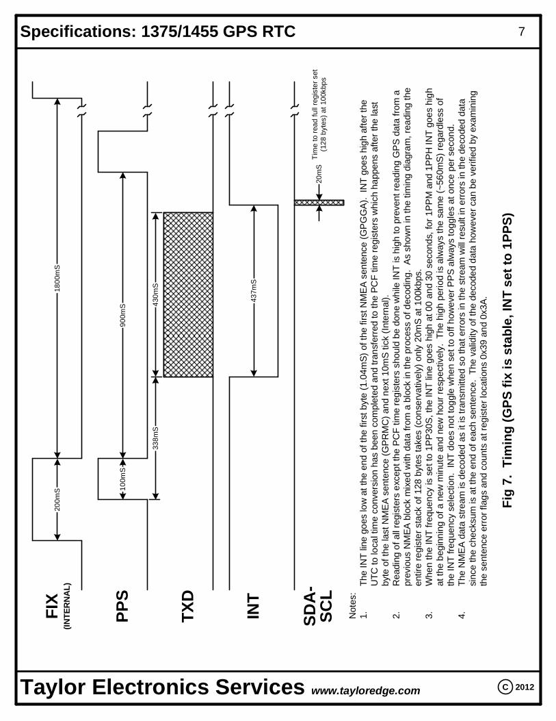
An interrupt output (INT) can be set to pulse high for 560mS every second (1PPS), 30 seconds(1PP30S), minute (1PPM), hour (1PPH) or off, The INT goes high after the GPS data has been fullydecoded and the local time calculation has been completed (Useful to control slave clocks). INT is lowduring NMEA sentence reception and then high during RS232 idle.
Three lamps indicate the status of the module: FIX blinks at 10Hz when the GPS indicates no fixis available, 2Hz if the fix signal is toggling faster than once per two seconds and solid on when a stablefix is indicated. PPS blinks at 1Hz 50% duty when the GPS PPS is stable at 1Hz 10% duty. MONblinks at 5Hz all the time and signals the main processing loop is running.
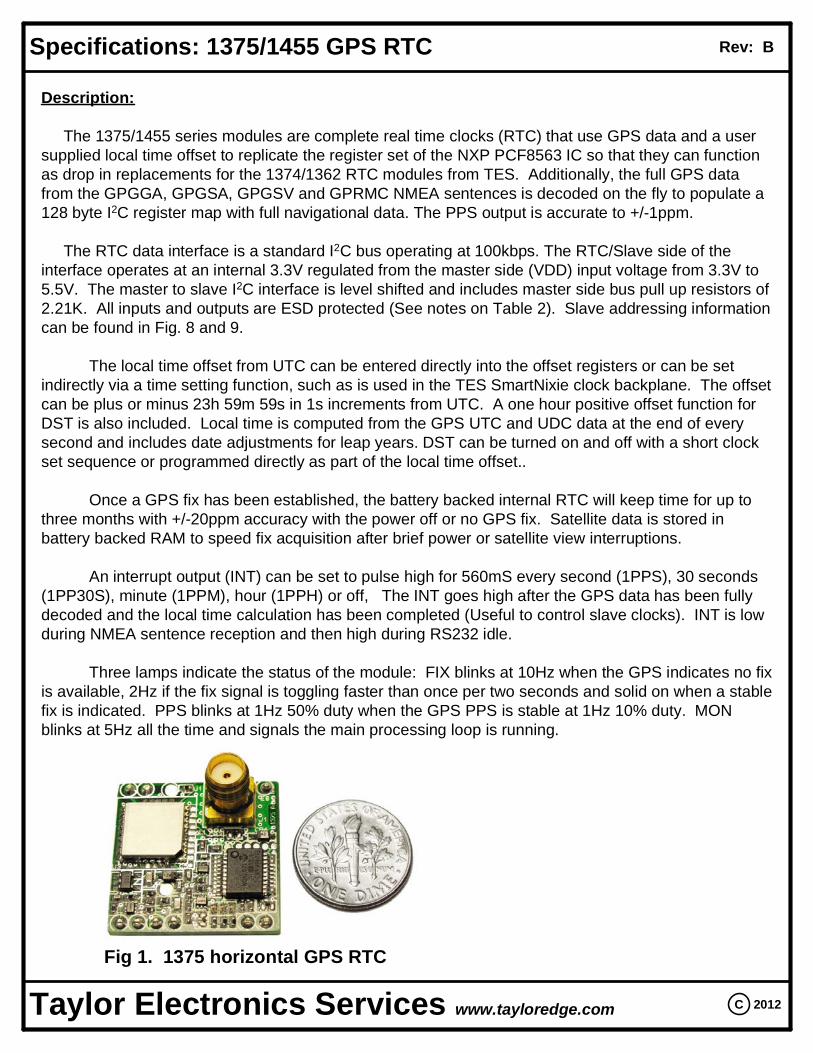
Fig 1. 1375 horizontal GPS RTC
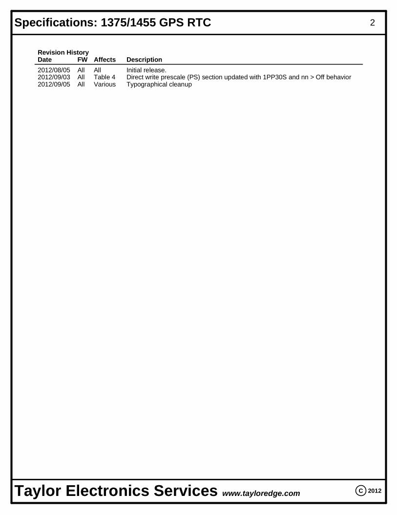
Revision HistoryDate FW Affects Description
Taylor Electronics Services www.tayloredge.com C 2012
Specifications: 1375/1455 GPS RTC 2
2012/08/05 All All Initial release.2012/09/03 All Table 4 Direct write prescale (PS) section updated with 1PP30S and nn > Off behavior2012/09/05 All Various Typographical cleanup
Taylor Electronics Services www.tayloredge.com C 2012
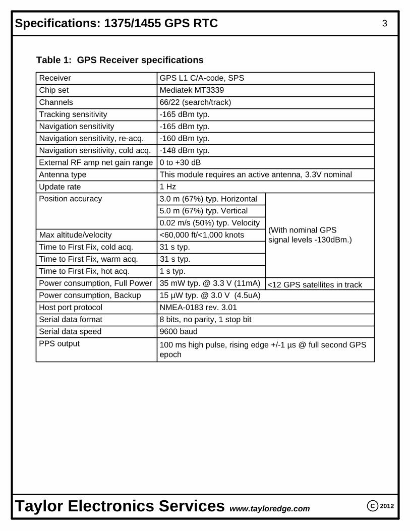
Update rate 1 HzPosition accuracy 3.0 m (67%) typ. Horizontal
5.0 m (67%) typ. Vertical0.02 m/s (50%) typ. Velocity
Max altitude/velocity <60,000 ft/<1,000 knotsTime to First Fix, cold acq. 31 s typ.Time to First Fix, warm acq. 31 s typ.Time to First Fix, hot acq. 1 s typ.Power consumption, Full Power 35 mW typ. @ 3.3 V (11mA) <12 GPS satellites in trackPower consumption, Backup 15 µW typ. @ 3.0 V (4.5uA)Host port protocol NMEA-0183 rev. 3.01Serial data format 8 bits, no parity, 1 stop bitSerial data speed 9600 baudPPS output 100 ms high pulse, rising edge +/-1 µs @ full second GPS
epoch
(With nominal GPSsignal levels -130dBm.)
Table 1: GPS Receiver specifications
External RF amp net gain range 0 to +30 dBAntenna type This module requires an active antenna, 3.3V nominal
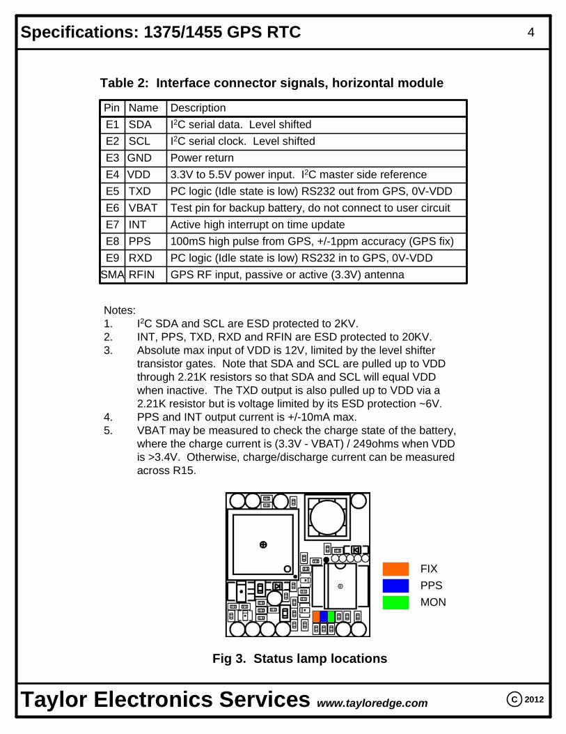
TXDVBATINTPPSRXD PC logic (Idle state is low) RS232 in to GPS, 0V-VDD
I2C serial data. Level shiftedI2C serial clock. Level shiftedPower return3.3V to 5.5V power input. I2C master side referencePC logic (Idle state is low) RS232 out from GPS, 0V-VDDTest pin for backup battery, do not connect to user circuitActive high interrupt on time update100mS high pulse from GPS, +/-1ppm accuracy (GPS fix)
VDD
Taylor Electronics Services www.tayloredge.com C 2012
Specifications: 1375/1455 GPS RTC 4
E2E3E4E5E6E7E8E9
SMA RFIN GPS RF input, passive or active (3.3V) antenna
Notes:1. I2C SDA and SCL are ESD protected to 2KV.2. INT, PPS, TXD, RXD and RFIN are ESD protected to 20KV.3. Absolute max input of VDD is 12V, limited by the level shifter
transistor gates. Note that SDA and SCL are pulled up to VDDthrough 2.21K resistors so that SDA and SCL will equal VDDwhen inactive. The TXD output is also pulled up to VDD via a2.21K resistor but is voltage limited by its ESD protection ~6V.
4. PPS and INT output current is +/-10mA max.5. VBAT may be measured to check the charge state of the battery,
where the charge current is (3.3V - VBAT) / 249ohms when VDDis >3.4V. Otherwise, charge/discharge current can be measuredacross R15.
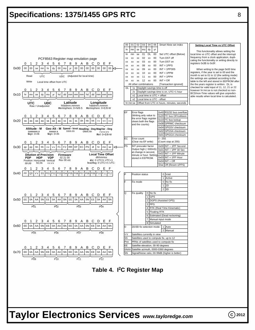
PS INT prescaler factorOutput high (~500mS)at change in second,minute or hour. Settingstored in EEPROM.
0x00 INT = 1PP Second
0x02 INT = 1PP Minute0x03 INT = 1PP Hour0x04 INT = Off
semnhr dymo yr
0001 DLhr mn se
Setting Local Time vs UTC Offset
This functionality allows setting thelocal time vs UTC offset and the interruptfrequency from a clock application, dupli-cating the functionality or writing directly toregisters 0x3B to 0x3F.
When writing to the page 0x00 timeregisters, if the year is set to 00 and themonth is set to 01 to 12 (the setting mode)the settings are updated according to thetable to the left and stored in EEPROM afterthe the years register is written. DL ischecked for valid input of 11, 12, 21 or 22however hr:mn:se is not checked so non-BCD/non-Time values will give unpredict-able results when local time is calculated.
Set UTC offset (Below)0002 xxxx xx xx Turn DST off0003 xxxx xx xx Turn DST on
DL Daylight savings time is offDaylight savings time is on, UTC+1 hour2x
1x
x1x2
Local time is UTC + offsetLocal time is UTC - offset
hr:mn:se Offset from UTC in hours, minutes, seconds
Else Off (Reset=1PPS)
08 00xxxx xx xx INT = 1PPS
10 00xxxx xx xx INT = 1PPM11 00xxxx xx xx INT = 1PPH12 00xxxx xx xx INT = Off
Firmware02 21 00
Rev 00 etc
09 00xxxx xx xx INT = 1PP30S
00 01 02 03 0504 Smart Nixie set index
0x20 I2C bus OF/collision
All other combinations [Transaction ignored]
Table 4. I2C Register Map
Taylor Electronics Services www.tayloredge.com C 2012
Specifications: 1375/1455 GPS RTC 8
0x01 INT = 1PP 30 Sec
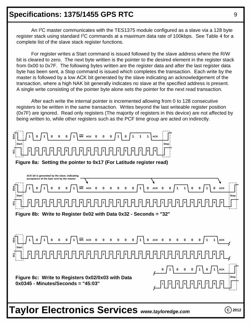
An I2C master communicates with the TES1375 module configured as a slave via a 128 byteregister stack using standard I2C commands at a maximum data rate of 100kbps. See Table 4 for acomplete list of the slave stack register functions.
For register writes a Start command is issued followed by the slave address where the R/Wbit is cleared to zero. The next byte written is the pointer to the desired element in the register stackfrom 0x00 to 0x7F. The following bytes written are the register data and after the last register databyte has been sent, a Stop command is issued which completes the transaction. Each write by themaster is followed by a low ACK bit generated by the slave indicating an acknowledgement of thetransaction, where a high NAK bit generally indicates no slave at the specified address is present.A single write consisting of the pointer byte alone sets the pointer for the next read transaction.
After each write the internal pointer is incremented allowing from 0 to 128 consecutiveregisters to be written in the same transaction. Writes beyond the last writeable register position(0x7F) are ignored. Read only registers (The majority of registers in this device) are not affected bybeing written to, while other registers such as the PCF time group are acted on indirectly.
StopStart
Figure 8b: Write to Register 0x02 with Data 0x32 - Seconds = "32"
ACK bit is generated by the slave, indicatingacceptance of the byte sent by the master.
Taylor Electronics Services www.tayloredge.com C 2012
Specifications: 1375/1455 GPS RTC 9
ACK1 WR 0 0 0 0 0 0 1 0 ACK1 10 0 0 0
ACK1 WR1 10 0 0 0 0 0 0 0 0 0 1 0 ACK
ACK1 0001100
11000000
0 1 110 0 0 0
ACK
ACK
StopStart
Figure 8a: Setting the pointer to 0x17 (For Latitude register read)
21 3 4 5 6 7 8 9 21 3 4 5 6 7 8 9
SDA
SCL
ACK1 WR 0 0 0 1 ACK1 10 0 0 0 1 110
Taylor Electronics Services www.tayloredge.com C 2012
Specifications: 1375/1455 GPS RTC 10
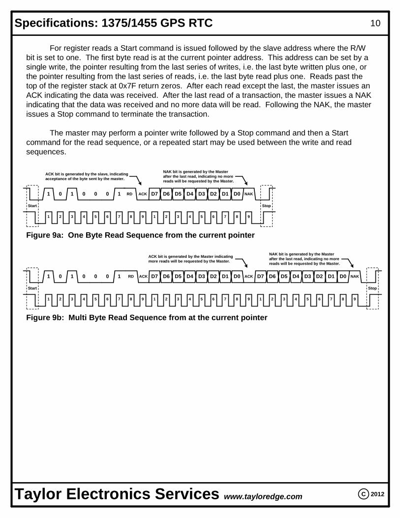
For register reads a Start command is issued followed by the slave address where the R/Wbit is set to one. The first byte read is at the current pointer address. This address can be set by asingle write, the pointer resulting from the last series of writes, i.e. the last byte written plus one, orthe pointer resulting from the last series of reads, i.e. the last byte read plus one. Reads past thetop of the register stack at 0x7F return zeros. After each read except the last, the master issues anACK indicating the data was received. After the last read of a transaction, the master issues a NAKindicating that the data was received and no more data will be read. Following the NAK, the masterissues a Stop command to terminate the transaction.
The master may perform a pointer write followed by a Stop command and then a Startcommand for the read sequence, or a repeated start may be used between the write and readsequences.
StopStart
ACK NAK
Figure 9a: One Byte Read Sequence from the current pointer
21 3 4 5 6 7 8 9 21 3 4 5 6 7 8 9
StopStart
ACK NAK
Figure 9b: Multi Byte Read Sequence from at the current pointer