18
Introduction to Electronic Circuit Design Richard R. Spencer Mohammed S. Ghausi
| Date post: | 14-Dec-2015 |
| Category: |
Documents |
| Upload: | alisha-turner |
| View: | 241 times |
| Download: | 3 times |

Introductionto
Electronic Circuit DesignRichard R. Spencer
Mohammed S. Ghausi

Figure 3-1 CMOS inverter

Figure 3-2 Cross section of the final CMOS integrated circuit. The PMOS transistor is shown on the left and the NMOS device is on the right. Remember that the bulk, or substrate, of each device is tied to its source (not shown in this cross section)

Figure 3-4 Mask #1 patterns the photoresist. The Si3N4 layer is removed by dry etching where it is not protected by the photoresist.
Following initial cleaning, an SiO2 layer is thermally grown on the silicon substrate. An Si3N4 layer is then deposited by LPCVD. Photoresist is spun on the wafer to prepare for the first masking operation. The result of the first masking operation is shown below in Figure 3-4.

Figure 3-6 Photoresist is used to mask the regions where PMOS devices will be built using Mask #2. A boron implant provides the doping for the P wells for the NMOS devices.
After the photoresist is stripped, the field oxide is grown. Then the Si3N4 layer is stripped off and a new layer of photoresist is spun on prior to Mask #2 being used. The result of using Mask #2 is shown in Figure 3-6 below.

Figure 3-7 Photoresist is used to mask the regions where NMOS devices will be built using Mask #3. A phosphorus implant provides the doping for the N wells for the PMOS devices.
The wells are then driven in by further high temperature processing.

Figure 3-9 After photoresist is spun onto the wafer, Mask #4 is used to define the NMOS transistors. A boron implant adjusts the N-channel Vth.
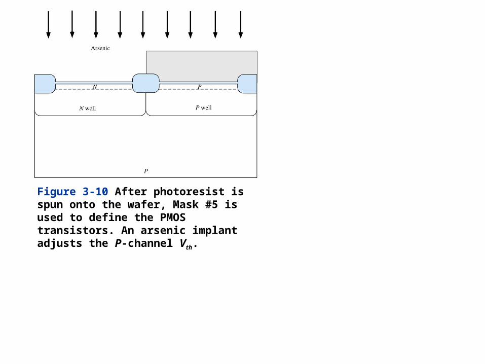
Figure 3-10 After photoresist is spun onto the wafer, Mask #5 is used to define the PMOS transistors. An arsenic implant adjusts the P-channel Vth.
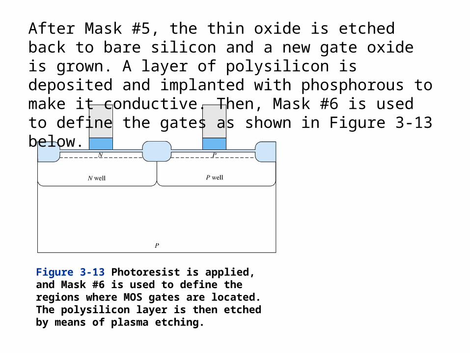
Figure 3-13 Photoresist is applied, and Mask #6 is used to define the regions where MOS gates are located. The polysilicon layer is then etched by means of plasma etching.
After Mask #5, the thin oxide is etched back to bare silicon and a new gate oxide is grown. A layer of polysilicon is deposited and implanted with phosphorous to make it conductive. Then, Mask #6 is used to define the gates as shown in Figure 3-13 below.
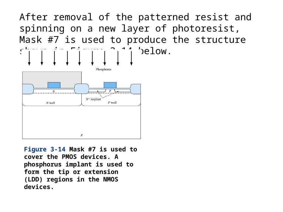
Figure 3-14 Mask #7 is used to cover the PMOS devices. A phosphorus implant is used to form the tip or extension (LDD) regions in the NMOS devices.
After removal of the patterned resist and spinning on a new layer of photoresist, Mask #7 is used to produce the structure shown in Figure 3-14 below.

Figure 3-15 Mask #8 is used to cover the NMOS devices. A boron implant is used to form the tip or extension (LDD) regions in the PMOS devices.
After removal of the patterned resist and spinning on a new layer of photoresist, Mask #8 is used to produce the structure shown in Figure 3-15 below.
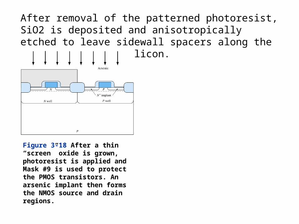
Figure 3-18 After a thin “screen” oxide is grown, photoresist is applied and Mask #9 is used to protect the PMOS transistors. An arsenic implant then forms the NMOS source and drain regions.
After removal of the patterned photoresist, SiO2 is deposited and anisotropically etched to leave sidewall spacers along the edges of the polysilicon.

Figure 3-19 After photoresist is applied, Mask #10 is used to protect the NMOS transistors. A boron implant then forms the PMOS source and drain regions.

Figure 3-24 Photoresist is applied and Mask #11 is used to define the regions where TiN local interconnects will be used. The TiN is then etched.
After Mask #10, a high-temperature drive in activates all the implanted dopants and diffuses junctions to their final depths. An unmasked then removes the oxide from the source and drain regions and from the top of the polysilicon. Titanium is then sputtered onto the surface and is reacted in an N2 ambient to form TiS2 where it contacts silicon or polysilicon and TiN elsewhere.
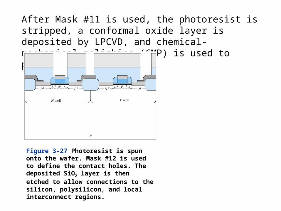
Figure 3-27 Photoresist is spun onto the wafer. Mask #12 is used to define the contact holes. The deposited SiO2 layer is then etched to allow connections to the silicon, polysilicon, and local interconnect regions.
After Mask #11 is used, the photoresist is stripped, a conformal oxide layer is deposited by LPCVD, and chemical-mechanical polishing (CMP) is used to planarize the surface.

Figure 3-29 Aluminum is deposited on the wafer by sputtering. Photoresist is spun onto the wafer, and Mask #13 is used to define the first level of metal. The Al is then plasma etched.
A thin TiN barrier-adhesion layer is deposited on the wafer by sputtering, followed by deposition of a W layer by CVD.

Figure 3-30 The steps to form the second level of Al interconnect follow those in Figures 3-25 through 3-29. Mask #14 is used to define via holes between metal 2 and metal 1. Mask #15 is used to define metal 2. The last step in the process is the deposition of a final passivation layer, usually Si3N4 deposited by PECVD. The last mask (#16) is used to open holes in this mask over the bonding pads.

Figure 3-31 Junction-isolated bipolar transistors. (a) A vertical npn transistor. (b) A lateral pnp transistor.


