Page 1
© December 22, 2013 Dr. Lynn Fuller
RIT MOSFET SPICE Parameters
Page 1
Rochester Institute of Technology
Microelectronic Engineering
ROCHESTER INSTITUTE OF TECHNOLOGY MICROELECTRONIC ENGINEERING
SPICE Model Parameters for RIT MOSFET’s
Dr. Lynn Fuller Microelectronic Engineering
Rochester Institute of Technology 82 Lomb Memorial Drive Rochester, NY 14623-5604
Tel (585) 475-2035 Fax (585) 475-5041
Dr. Fuller’s Webpage: http://people.rit.edu/lffeee
Email: [email protected] Dept Webpage: http://www.microe.rit.edu
12-10-2013 SPICE_MOSFET_Models.ppt
Page 2
© December 22, 2013 Dr. Lynn Fuller
RIT MOSFET SPICE Parameters
Page 2
Rochester Institute of Technology
Microelectronic Engineering
OUTLINE
Introduction
SPICE Level 1 Model
SPICE Level 3 Model
BSIM3 Model
SPICE Parameter Calculator
SPICE Parameters for RIT MOSFETs
Winspice
Examples
Parameter Extraction Using UTMOST
ATHENA > ATLAS > UTMOST > SPICE
References
Page 3
© December 22, 2013 Dr. Lynn Fuller
RIT MOSFET SPICE Parameters
Page 3
Rochester Institute of Technology
Microelectronic Engineering
SPICE - SIMULATION PROGRAM FOR INTEGRATED CIRCUIT ENGINEERING
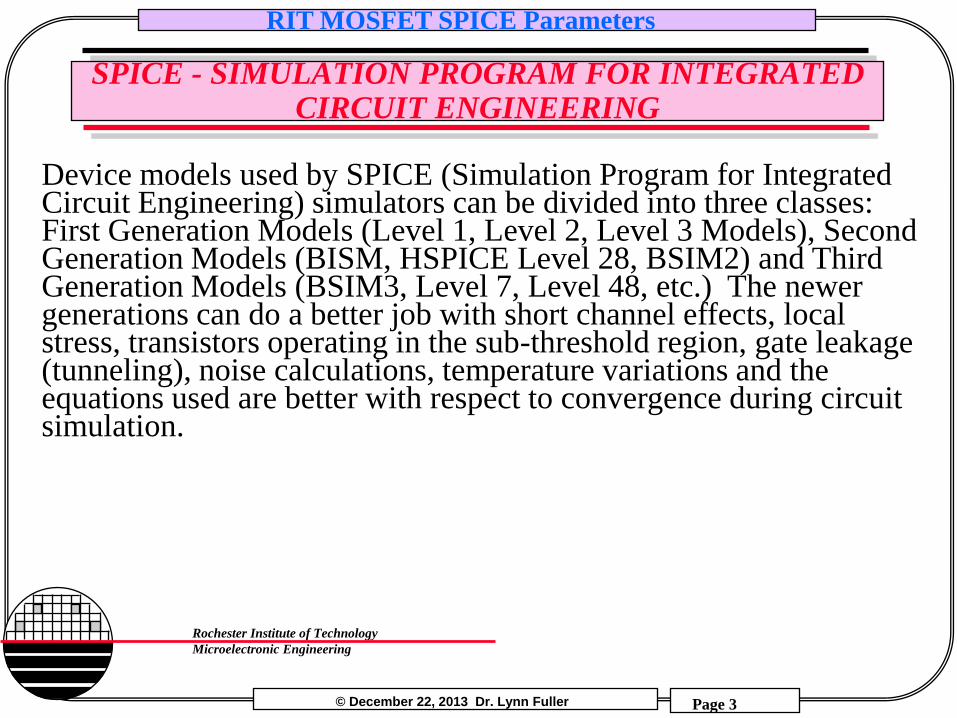
Device models used by SPICE (Simulation Program for Integrated Circuit Engineering) simulators can be divided into three classes: First Generation Models (Level 1, Level 2, Level 3 Models), Second Generation Models (BISM, HSPICE Level 28, BSIM2) and Third Generation Models (BSIM3, Level 7, Level 48, etc.) The newer generations can do a better job with short channel effects, local stress, transistors operating in the sub-threshold region, gate leakage (tunneling), noise calculations, temperature variations and the equations used are better with respect to convergence during circuit simulation.
Page 4
© December 22, 2013 Dr. Lynn Fuller
RIT MOSFET SPICE Parameters
Page 4
Rochester Institute of Technology
Microelectronic Engineering
SPICE LEVEL-1 SHICHMAN AND HODGES
If we understand the Level 1 model we can better understand the other models. The Level 1 model by Shichman and Hodges uses basic device physics equations for MOSFET threshold voltage and drain current in the saturation and non-saturation regions of operation. Mobility is assumed to be a function of total doping concentration only and a parameter called LAMBDA is used to model channel length modulation.
David A. Hodges [email protected]
Page 5
© December 22, 2013 Dr. Lynn Fuller
RIT MOSFET SPICE Parameters
Page 5
Rochester Institute of Technology
Microelectronic Engineering
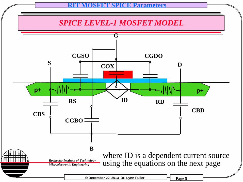
SPICE LEVEL-1 MOSFET MODEL
p+ p+
CBD
S
G
D
CBS
RS RD
CGDO
ID
CGBO
COX
CGSO
B
where ID is a dependent current source using the equations on the next page
Page 6
© December 22, 2013 Dr. Lynn Fuller
RIT MOSFET SPICE Parameters
Page 6
Rochester Institute of Technology
Microelectronic Engineering
SPICE LEVEL-1 EQUATIONS FOR UO, Vto AND ID
Parameter Arsenic Phosphorous Boron
µmin 52.2 68.5 44.9
µmax 1417 1414 470.5
Nref 9.68X10^16 9.20X10^16 2.23X10^17
0.680 0.711 0.719
µ = µ min+ (µmax-µmin)
{1 + (N/Nref) }
Mobility:
Threshold Voltage:
+/-
nmos/pmos
Drain Current: Non-Saturation
Saturation
ID = µW Cox’ (Vg-Vt-Vd/2)Vd (1+ Vds)
L
IDsat = µW Cox’ (Vg-Vt)2 (1+ Vds)
2L
VTO = ms - q NSS/Cox’+/ -2[ F] +/-2 (q s NSUB [ F])0.5/Cox’
F] = (KT/q ) ln (NSUB/ni) where ni = 1.45E10 and KT/q = 0.026 Absolute value
Cox’= r o/TOX=3.9 o/TOX
Page 7
© December 22, 2013 Dr. Lynn Fuller
RIT MOSFET SPICE Parameters
Page 7
Rochester Institute of Technology
Microelectronic Engineering
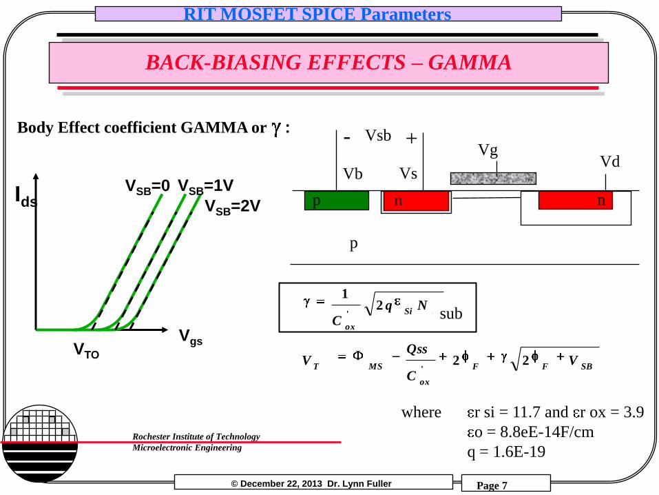
BACK-BIASING EFFECTS – GAMMA
Body Effect coefficient GAMMA or :
SBFF
ox
MST
ASi
ox
V
C
QssV
Nq
C
LC
22
21
'
'
Ids
Vgs
VSB=0
VSB=2V
VSB=1V n n
Vs
Vg Vd
p
p
Vb
Vsb + -
where r si = 11.7 and r ox = 3.9
o = 8.8eE-14F/cm
q = 1.6E-19
VTO
sub
Page 8
© December 22, 2013 Dr. Lynn Fuller
RIT MOSFET SPICE Parameters
Page 8
Rochester Institute of Technology
Microelectronic Engineering Non Saturation Region
CHANNEL LENGTH MODULATION - LAMBDA
IDsat = µW Cox’ (Vg-Vt)2 (1+ Vds) NMOS Transistor
2L DC Model, is the channel length modulation
parameter and is different for each channel
length, L. Typical value might be 0.02
Channel Length Modulation
Parameter
= Slope/ Idsat
n n
S Vg Vd
p
L L - L
Vd1 Vd2
Slope +Ids
+Vgs
+Vds
NMOS
+5
+4 +3
+2
Saturation Region
Vd1 Vd2
Idsat
ID = µW Cox’ (Vg-Vt-Vd/2)Vd (1+ Vds)
L
Saturation Region
Page 9
© December 22, 2013 Dr. Lynn Fuller
RIT MOSFET SPICE Parameters
Page 9
Rochester Institute of Technology
Microelectronic Engineering
LAMBDA VERSUS CHANNEL LENGTH
µA LAMBDA
UNIT SLOPE IDSAT W L PMOS NMOS
205 4.9 6.8 32 2 0.144118 0.132308
71 2 7.1 32 4 0.056338 0.026761
56 1.8 7.3 32 6 0.049315 0.011429
34 1.2 7.5 32 8 0.032 0.013889
21 1 7 32 16 0.028571 0.005556
8.8 0.8 7.6 32 32 0.021053 0.004196
415 4.3 6.5 32 2 0.132308
137 0.95 7.1 32 4 0.026761
91 0.4 7 32 6 0.011429
137 0.5 7.2 32 8 0.013889
27 0.2 7.2 32 16 0.005556
15 0.15 7.15 32 32 0.004196
y = 0.1351x-1.014
0
0.02
0.04
0.06
0.08
0.1
0.12
0.14
0.16
2 4 6 8 16 32
LA
MB
DA
LENGTH
LAMBDA
PMOS
NMOS
Power (PMOS)
Need different model for each different length transistor
Page 10
© December 22, 2013 Dr. Lynn Fuller
RIT MOSFET SPICE Parameters
Page 10
Rochester Institute of Technology
Microelectronic Engineering
SPICE LEVEL-1 PARAMETERS
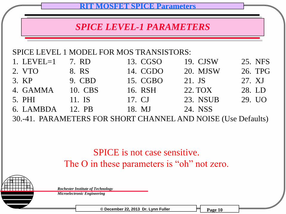
SPICE LEVEL 1 MODEL FOR MOS TRANSISTORS:
1. LEVEL=1 7. RD 13. CGSO 19. CJSW 25. NFS
2. VTO 8. RS 14. CGDO 20. MJSW 26. TPG
3. KP 9. CBD 15. CGBO 21. JS 27. XJ
4. GAMMA 10. CBS 16. RSH 22. TOX 28. LD
5. PHI 11. IS 17. CJ 23. NSUB 29. UO
6. LAMBDA 12. PB 18. MJ 24. NSS
30.-41. PARAMETERS FOR SHORT CHANNEL AND NOISE (Use Defaults)
SPICE is not case sensitive.
The O in these parameters is “oh” not zero.
Page 11
© December 22, 2013 Dr. Lynn Fuller
RIT MOSFET SPICE Parameters
Page 11
Rochester Institute of Technology
Microelectronic Engineering
SPICE LEVEL-1 PARAMETERS FOR MOSFET (cont.)
1. LEVEL=1 Shichman-Hodges Model (If not specified the default is LEVEL=1)
2. VTO zero bias threshold voltage (Do not use, let SPICE calculate from Nsub,TOX
unless an VT adjust ion implant is used to set VTO at some value)
+Vg
+Id
VTO
Vsub = 0
-2
-1
-3 volts
+Ids
+Vgs
+Vds
+5
+4 +3
+2
Saturation Region
VTO
3. KP transconductance parameter (Do not use, let SPICE calculate from UO, COX’)
KP = UO COX’ = UO r o / TOX
Page 12
© December 22, 2013 Dr. Lynn Fuller
RIT MOSFET SPICE Parameters
Page 12
Rochester Institute of Technology
Microelectronic Engineering
SPICE LEVEL-1 PARAMETERS FOR MOSFET (cont.)
4. GAMMA bulk threshold parameter (Do not use, let SPICE calculate from NSUB,COX’)
GAMMA = [2q rsi o NSUB/C’ox2]1/2 where si o = (11.7)(8.85E-12)
and q = 1.6E-19
5. PHI is the surface inversion potential, 2 x Intrinsic Level to Fermi Level
difference in Volts (Do not use, let SPICE calculate from NSUB)
PHI = 2[ F] = 2 (KT/q) ln (NSUB/ni) where KT/q = 0.026
ni = 1.45E10
6. LAMBDA is the channel length modulation parameter, Slope in saturation
region divided by Idsat
= Slope/ Idsat
Slope +Ids
+Vgs
+Vds
+5 +4 +3
+2
Saturation Region
Vd1 Vd2
Idsat
Page 13
© December 22, 2013 Dr. Lynn Fuller
RIT MOSFET SPICE Parameters
Page 13
Rochester Institute of Technology
Microelectronic Engineering
SPICE LEVEL-1 PARAMETERS FOR MOSFET (cont.)
7. RD the series drain resistance can either be given as a resistance value or
through RSH the drain/source sheet resistance and the number of squares NRS.
NRS: Is from the device layout. RSH: Is measured by four point probe or Van Der
Pauw structures (Do not use, let SPICE calculate from sheet resistance, RSH, and number of squares in drain,
NRD)
8. RS is the series source resistance can either be given as a resistance value or
through RSH the drain/source sheet resistance and the number of squares NRS.
NRS: Is from the device layout. RSH: Is measured by four point probe or Van Der
Pauw structures
(Do not use, let SPICE calculate from sheet resistance, RSH, and number of squares in
source, NRS)
Page 14
© December 22, 2013 Dr. Lynn Fuller
RIT MOSFET SPICE Parameters
Page 14
Rochester Institute of Technology
Microelectronic Engineering
SPICE LEVEL-1 PARAMETERS FOR MOSFET (cont.)
9. CBD zero bias bulk to drain junction capacitance (Do not use, let SPICE
calculate from CJ and CJSW and AD (Area of Drain) and PD (Perimeter of Drain)
CBD = CJ AD + CJSW PD
10. CBS zero bias bulk to source junction capacitance (Do not use, let SPICE
calculate from CJ and CJSW and AS (Area of Source) and PD (Perimeter of Source)
CBS = CJ AS + CJSW PS
11. IS is the bulk junction saturation current in the ideal diode equation.
I = IS (exp qVA/KT - 1)
(Do not use, let SPICE calculate from JS and AD (Area of Drain) and AS (Area of Source)
IS = JS (AD + AS)
12. PB is the junction built in voltage
PB = (KT/q)ln (NSUB/ni) + 0.56 or PB = (KT/q) ln (Na Nd/ni2)
Page 15
© December 22, 2013 Dr. Lynn Fuller
RIT MOSFET SPICE Parameters
Page 15
Rochester Institute of Technology
Microelectronic Engineering
SPICE LEVEL-1 PARAMETERS FOR MOSFET (cont.)
13. CGSO is the gate-to-source overlap capacitance (per meter channel width)
CGSO = Cox’ (mask overlap in L direction + LD) F/m
14. CGDO is the gate-to-drain overlap capacitance (per meter channel width)
CGDO = Cox’ (mask overlap in L direction + LD) F/m
15. CGBO is the gate-to-bulk overlap capacitance (per meter channel length)
CGBO = Cfield_oxide * mask overlap in W direction F/m
Cfield_oxide = r o/XFieldOX
Cox’ = r o/TOX=3.9 o/TOX
Page 16
© December 22, 2013 Dr. Lynn Fuller
RIT MOSFET SPICE Parameters
Page 16
Rochester Institute of Technology
Microelectronic Engineering
SPICE LEVEL-1 PARAMETERS FOR MOSFET (cont.)
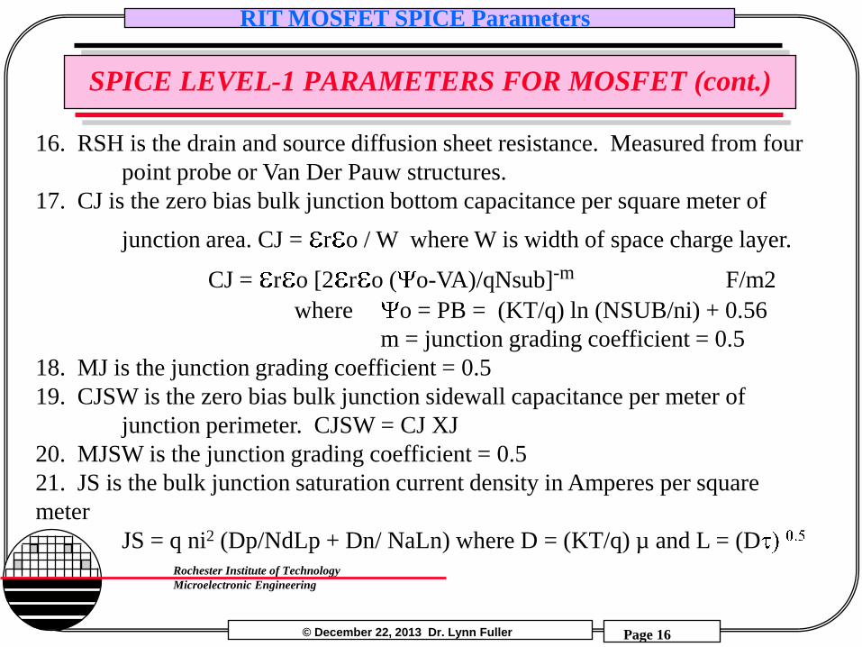
16. RSH is the drain and source diffusion sheet resistance. Measured from four
point probe or Van Der Pauw structures.
17. CJ is the zero bias bulk junction bottom capacitance per square meter of
junction area. CJ = r o / W where W is width of space charge layer.
CJ = r o [2 r o ( o-VA)/qNsub]-m F/m2
where o = PB = (KT/q) ln (NSUB/ni) + 0.56
m = junction grading coefficient = 0.5
18. MJ is the junction grading coefficient = 0.5
19. CJSW is the zero bias bulk junction sidewall capacitance per meter of
junction perimeter. CJSW = CJ XJ
20. MJSW is the junction grading coefficient = 0.5
21. JS is the bulk junction saturation current density in Amperes per square
meter
JS = q ni2 (Dp/NdLp + Dn/ NaLn) where D = (KT/q) µ and L = (D
Page 17
© December 22, 2013 Dr. Lynn Fuller
RIT MOSFET SPICE Parameters
Page 17
Rochester Institute of Technology
Microelectronic Engineering
SPICE LEVEL-1 PARAMETERS FOR MOSFET (cont.)
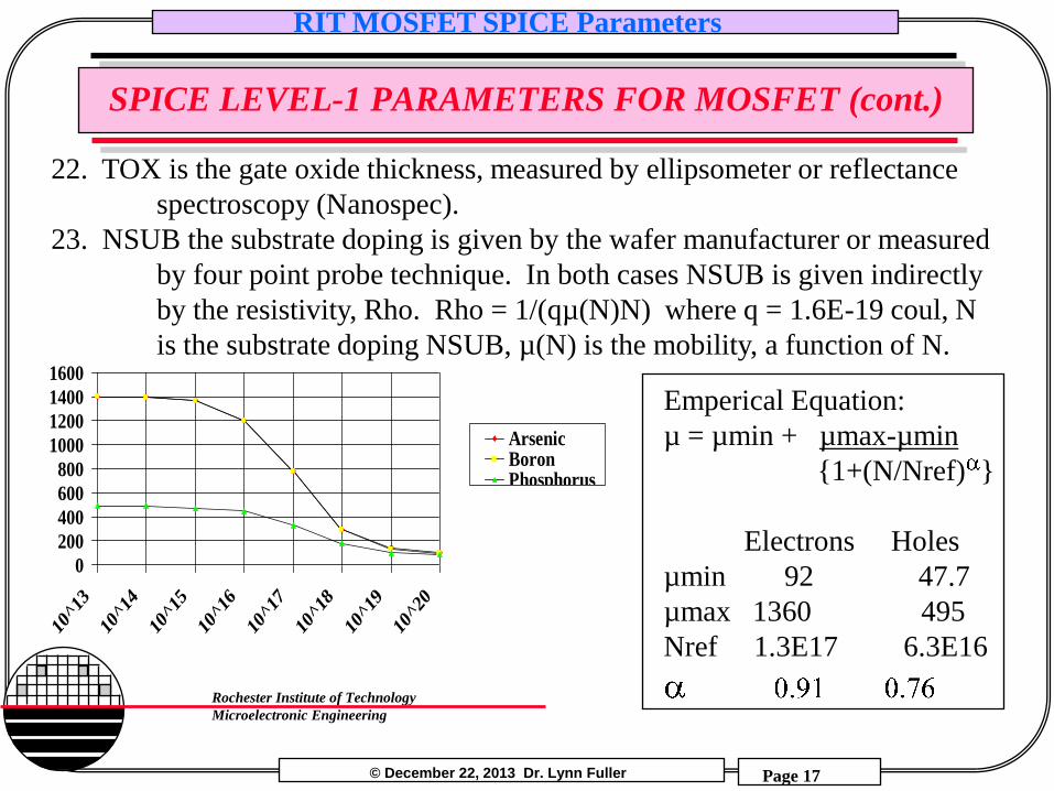
22. TOX is the gate oxide thickness, measured by ellipsometer or reflectance
spectroscopy (Nanospec).
23. NSUB the substrate doping is given by the wafer manufacturer or measured
by four point probe technique. In both cases NSUB is given indirectly
by the resistivity, Rho. Rho = 1/(qµ(N)N) where q = 1.6E-19 coul, N
is the substrate doping NSUB, µ(N) is the mobility, a function of N.
Emperical Equation:
µ = µmin + µmax-µmin
{1+(N/Nref) }
Electrons Holes
µmin 92 47.7
µmax 1360 495
Nref 1.3E17 6.3E16
0
200
400
600
800
1000
1200
1400
1600
10^1
3
10^1
4
10^1
5
10^1
6
10^1
7
10^1
8
10^1
9
10^2
0
ArsenicBoronPhosphorus
Page 18
© December 22, 2013 Dr. Lynn Fuller
RIT MOSFET SPICE Parameters
Page 18
Rochester Institute of Technology
Microelectronic Engineering
SPICE LEVEL-1 PARAMETERS FOR MOSFET (cont.)
25. NFS is the fast surface state density, usually left at zero.
24. NSS: The surface state density is a parameter used in the calculation of the zero-
bias threshold voltage (ie. Vsource = Vsubstrate), VT0 is obtained from transistor
curves.
VTO = ms - q NSS/Cox’ -2 F -2 (q s NSUB F)^0.5/Cox’
F = (KT/q ) ln (NSUB/ni) where ni = 1.45E10 and KT/q = 0.026
ms = m - ( + Eg/2 - F) where m=gate work function
= 4.15 eV, Eg = 1.12 eV
s = r o = 11.7 o Since everything is known
Cox’= r o/TOX=3.9 o/TOX in equations above, NSS can be calculated
Page 19
© December 22, 2013 Dr. Lynn Fuller
RIT MOSFET SPICE Parameters
Page 19
Rochester Institute of Technology
Microelectronic Engineering
SPICE LEVEL-1 PARAMETERS FOR MOSFET (cont.)
26. TPG is the type of gate. for aluminum TPG=0, for n+ poly TPG = 1,
for p+ poly TPG= -1
27. XJ metallurgical junction depth, measured by groove and stain techniques.
28. LD lateral diffusion distance, inferred from process knowledge
29. UO is the surface mobility taken as 1/2 the bulk mobility or
extracted to give correct Id value on measured Id vs Vds characteristics
in the saturation region. For best results make measurements on a transistor with
large channel length so that is small and the lateral diffusion can be neglected.
IDsat = µW Cox’ (Vg-Vt)2 (1+ Vds)
2L 30. - 41. Parameters associated with short channel devices and noise in
MOSFETs
Page 20
© December 22, 2013 Dr. Lynn Fuller
RIT MOSFET SPICE Parameters
Page 20
Rochester Institute of Technology
Microelectronic Engineering
SPICE 2ND GENERATION MODELS AND PARAMETERS
2ND generation MOSFET models improve over the Level 1 models because they model sub-threshold current, mobility as a function of vertical and lateral electric field strength, threshold voltage reduction as a function drain voltage or drain induced barrier lowering (DIBL). This model has separate equations for drain current for different regions of operation. The discontinuity at the transition points can make problems in program convergence during circuit simulation.
Note: LEVEL 1 model Id would follow green line
Note: LEVEL 1 model Id would increase with (Vgs-Vt)2
Page 21
© December 22, 2013 Dr. Lynn Fuller
RIT MOSFET SPICE Parameters
Page 21
Rochester Institute of Technology
Microelectronic Engineering
TERADA-MUTA METHOD FOR EXTRACTING Leff and Rds
In the linear region (VD is small):
ID = µW Cox’ (Vg-Vt-Vd/2) VD
Leff
0 Leff = Lm - L
where L is correction due to processing
Lm is the mask length
Rm = VD/ID = measured resistance
= Lm/ (µW Cox’ (Vg-Vt)) - L/ µW Cox’ (Vg-Vt)
so measure Rm for different channel length transistors and plot Rm vs Lm
where Rm = intersect find value for L and Rds
Then Leff can be calculated for each different length transistor
from Leff = Lm - L
Vg = -6
Vg = -10
Vg = -8
Lm (mask length)
Ma
sure
d R
esis
tan
ce,
Rm
L
Terada-Muta Method for Leff and Rds
Rds
I D = 1/Rm VD
Page 22
© December 22, 2013 Dr. Lynn Fuller
RIT MOSFET SPICE Parameters
Page 22
Rochester Institute of Technology
Microelectronic Engineering
2nd GENERATION MODELS EQUATIONS FOR MOBILITY
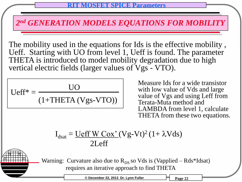
The mobility used in the equations for Ids is the effective mobility , Ueff. Starting with UO from level 1, Ueff is found. The parameter THETA is introduced to model mobility degradation due to high vertical electric fields (larger values of Vgs - VTO).
Ueff* = (1+THETA (Vgs-VTO))
UO
Warning: Curvature also due to RDS so Vds is (Vapplied – Rds*Idsat)
requires an iterative approach to find THETA
Idsat = Ueff W Cox’ (Vg-Vt)2 (1+ Vds)
2Leff
Measure Ids for a wide transistor with low value of Vds and large value of Vgs and using Leff from Terata-Muta method and LAMBDA from level 1, calculate THETA from these two equations.
Page 23
© December 22, 2013 Dr. Lynn Fuller
RIT MOSFET SPICE Parameters
Page 23
Rochester Institute of Technology
Microelectronic Engineering
2ND GENERATION EQUATIONS FOR MOBILITY (cont.)
The parameter VMAX is introduced to model the decrease in mobility at higher Vds due to velocity saturation. Ideally, carrier velocity is directly proportional to the applied electric field. However, at very high lateral electric fields, Ex, this relationship ceases to be accurate - the carrier velocity saturates at VMAX.
Where, Vde = min (Vds, Vdsat)
Ueff = UO
1 + UO VMAX Leff
vde
Note: other models (equations) for
mobility exist and use parameters such as
UCRIT, UEXP, ULTRA, ECRIT, ESAT
Ex
(V/cm)
Vel
oci
ty (
cm/s
ec)
105
107
106
103 104 105
= UO Ex
VMAX
(1+THETA (Vgs-VTO))
Page 24
© December 22, 2013 Dr. Lynn Fuller
RIT MOSFET SPICE Parameters
Page 24
Rochester Institute of Technology
Microelectronic Engineering
2ND GENERATION MODEL EUATIONS FOR THRESHOLD VOLTAGE
The parameter ETA is used to describe DIBL (Drain Induced Barrier Lowering) resulting in a modification to the LEVEL 1 equation for threshold voltage.
VTO = ms- - q NSS/Cox’ -2 F -2 (q s NSUB F)0.5/Cox’
(- 8.14E-22)*ETA
Cox’Leff 3
Vds
Page 25
© December 22, 2013 Dr. Lynn Fuller
RIT MOSFET SPICE Parameters
Page 25
Rochester Institute of Technology
Microelectronic Engineering
2ND GENERATION EQUATIONS FOR NARROW WIDTH
DELTA is introduced to model narrow channel effects on threshold voltage. The parameter WD (channel width reduction from drawn value) is used to calculate the effective channel width. DELTA is used in the calculation of threshold voltage.
q NSUB Xds2
o si 2 PHI
DELTA =
Note: a dimensionless number typically ~3
Page 26
© December 22, 2013 Dr. Lynn Fuller
RIT MOSFET SPICE Parameters
Page 26
Rochester Institute of Technology
Microelectronic Engineering
2ND GENERATION EQUATIONS FOR CHANNEL LENGTH MODULATION
KAPPA is channel length modulation parameter.
KAPPA is calculated = [(qNsub/(2 o r))((1-Idsat/Id')(L-2LD-Xdso-Xds))^2)/(Vd2-Vdsat)]^0.5
Measure Id’ at large Vds, and Idsat at Vdsat,
Kappa has units of 1/V typical value ~0.1
+Ids
+Vgs
+Vds
+5 +4 +3
+2
Saturation Region
Vdsat Vd2
Idsat
Id’ n n
Vs Vg Vd
p
L
L - L Vdsat
Vd2
Ld Ld
Xdso Xds
Page 27
© December 22, 2013 Dr. Lynn Fuller
RIT MOSFET SPICE Parameters
Page 27
Rochester Institute of Technology
Microelectronic Engineering
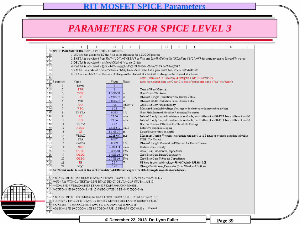
PARAMETERS FOR SPICE LEVEL 3
SPICE LEVEL 3 MODEL PARAMETERS FOR MOS TRANSISTORS: Control Level=3 Process TPG=1 1 if gate is doped opposite of channel, -1 if not Process TOX Gate Oxide Thickness Process NSUB Channel doping concentration Process XJ Drain/Source Junction Depth Process PB PB is the junction built in voltage W and L LD Drain/Source Lateral Diffusion W and L WD Decrease in Width from Drawn Value DC UO Zero Bias Low Field Mobility DC VTO Measured threshold voltage, long wide devices DC THETA Gate Field Induced Mobility Reduction DC DELTA Narrow Channel Effect on the Threshold Voltage DC VMAX Maximum Carrier Velocity DC ETA DIBL Coefficient DC KAPPA Channel Length Modulation Effect on Ids DC NFS Surface State Density
Page 28
© December 22, 2013 Dr. Lynn Fuller
RIT MOSFET SPICE Parameters
Page 28
Rochester Institute of Technology
Microelectronic Engineering
PARAMETERS FOR SPICE LEVEL 3
Diode & Resistor RS Source Series Resistance Diode & Resistor RD Drain Series Resistance AC CGDO Zero Bias Gate-Source Capacitance AC CGSO Zero Bias Gate-Drain Capacitance AC CGBO Zero Bias Gate-Substrate Capacitance AC CJ Temp - more Noise - more Tunneling -more
Page 29
© December 22, 2013 Dr. Lynn Fuller
RIT MOSFET SPICE Parameters
Page 29
Rochester Institute of Technology
Microelectronic Engineering
BSIM3 MODELS
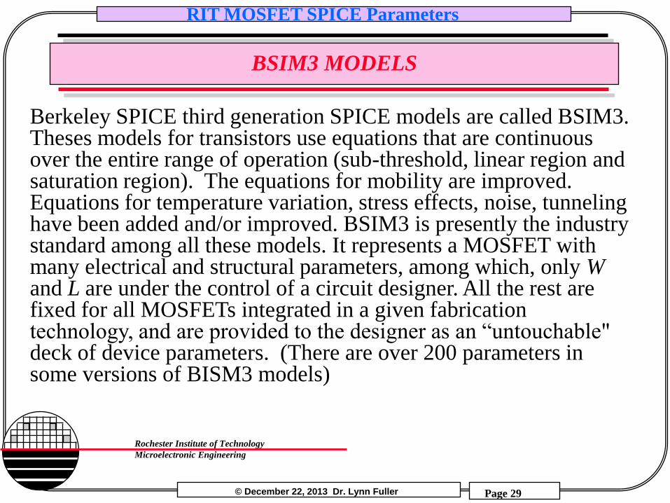
Berkeley SPICE third generation SPICE models are called BSIM3. Theses models for transistors use equations that are continuous over the entire range of operation (sub-threshold, linear region and saturation region). The equations for mobility are improved. Equations for temperature variation, stress effects, noise, tunneling have been added and/or improved. BSIM3 is presently the industry standard among all these models. It represents a MOSFET with many electrical and structural parameters, among which, only W and L are under the control of a circuit designer. All the rest are fixed for all MOSFETs integrated in a given fabrication technology, and are provided to the designer as an “untouchable" deck of device parameters. (There are over 200 parameters in some versions of BISM3 models)
Page 30
© December 22, 2013 Dr. Lynn Fuller
RIT MOSFET SPICE Parameters
Page 30
Rochester Institute of Technology
Microelectronic Engineering
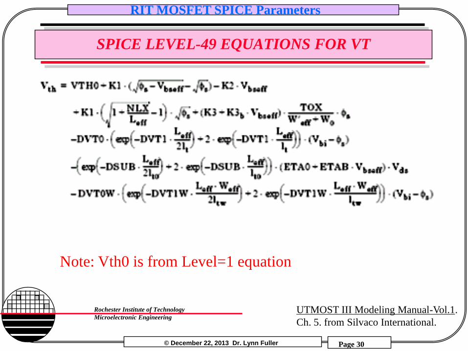
SPICE LEVEL-49 EQUATIONS FOR VT
UTMOST III Modeling Manual-Vol.1.
Ch. 5. from Silvaco International.
Note: Vth0 is from Level=1 equation
Page 31
© December 22, 2013 Dr. Lynn Fuller
RIT MOSFET SPICE Parameters
Page 31
Rochester Institute of Technology
Microelectronic Engineering
SPICE LEVEL-49 EQUATIONS FOR UO
UA, UB and UC are emperically fit and replace THETA and VMAX used in LEVEL 3
n=1 + NFACTOR *Cd/COX + ((CDSC + CDSCD*Vds + CDSCB*Vbseff) – (exp(-DVT1*Leff/2lt) + 2exp(-DVT1*Leff/lt)))/COX + CIT/C0X
UTMOST III Modeling Manual-Vol.1.
Ch. 5. from Silvaco International.
Page 32
© December 22, 2013 Dr. Lynn Fuller
RIT MOSFET SPICE Parameters
Page 32
Rochester Institute of Technology
Microelectronic Engineering
SPICE LEVEL-49 EQUATIONS FOR ID
UTMOST III Modeling Manual-Vol.1.
Ch. 5. from Silvaco International.
Page 33
© December 22, 2013 Dr. Lynn Fuller
RIT MOSFET SPICE Parameters
Page 33
Rochester Institute of Technology
Microelectronic Engineering
SPICE LEVEL-49 EQUATIONS FOR ID (cont)
UTMOST III Modeling Manual-Vol.1.
Ch. 5. from Silvaco International.
Page 34
© December 22, 2013 Dr. Lynn Fuller
RIT MOSFET SPICE Parameters
Page 34
Rochester Institute of Technology
Microelectronic Engineering
PARAMETERS FOR SPICE BSIM3 LEVEL 49
SPICE BSIM3 LEVEL 49 MODEL PARAMETERS FOR MOS TRANSISTORS:
Control LEVEL=49
Control MOBMOD=1 Mobility model selector choice
Control CAPMOD=1 Capacitor model selector choice
Process TOX Gate Oxide Thickness
Process XJ Drain/Source Junction Depth
Process NCH Channel Surface doping concentration
Process NSUB Channel doping concentration
Process XT Distance into the well where NCH is valid
Process NSF Fast Surface State Density
Process NGATE Gate Doping Concentration
W and L WINT Isolation Reduction of Channel Width
W and L LINT Source/Drain Underdiffusion of Gate
Note: only some of the few hundred parameters
Page 35
© December 22, 2013 Dr. Lynn Fuller
RIT MOSFET SPICE Parameters
Page 35
Rochester Institute of Technology
Microelectronic Engineering
PARAMETERS FOR SPICE BSIM3 LEVEL 49
DC VTH0 Threshold voltage, Long, Wide Device, Zero Substrate Bias = VTO in level 3 DC U0 Low Field Mobility, UO in level 3 DC PCLM Channel Length Modulation Parameter Diode & Resistor RSH Drain/Source sheet Resistance Diode & Resistor JS Bottom junction saturation current per unit area Diode & Resistor JSW Side wall junction saturation current per unit length Diode & Resistor CJ Bottom Junction Capacitance per unit area at zero bias Diode & Resistor MJ Bottom Junction Capacitance Grading Coeficient Diode & Resistor PB PB is the junction built in voltage Diode & Resistor CJSW Side Wall Junction Capacitance per meter of length Diode & Resistor MJSW Side Wall Junction Capacitance Grading Coeficient AC CGSO Zero Bias Gate-Source Capacitance per meter of gate W AC CGDO Zero Bias Gate-Drain Capacitance per meter of gate W AC CGBO Zero Bias Gate-Substrate Capacitance per meter of gate L
Note: only some of the few hundred parameters
Page 36
© December 22, 2013 Dr. Lynn Fuller
RIT MOSFET SPICE Parameters
Page 36
Rochester Institute of Technology
Microelectronic Engineering
EXCEL SPREADSHEET SPICE PARAMETER CALCULATOR
SPICE Parameter Calculator.xls
Page 37
© December 22, 2013 Dr. Lynn Fuller
RIT MOSFET SPICE Parameters
Page 37
Rochester Institute of Technology
Microelectronic Engineering
INPUTS AND RESULTS
Page 38
© December 22, 2013 Dr. Lynn Fuller
RIT MOSFET SPICE Parameters
Page 38
Rochester Institute of Technology
Microelectronic Engineering
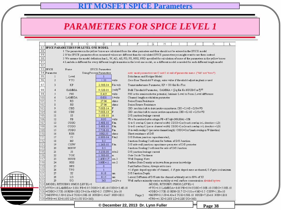
PARAMETERS FOR SPICE LEVEL 1
Page 39
© December 22, 2013 Dr. Lynn Fuller
RIT MOSFET SPICE Parameters
Page 39
Rochester Institute of Technology
Microelectronic Engineering
PARAMETERS FOR SPICE LEVEL 3
Page 40
© December 22, 2013 Dr. Lynn Fuller
RIT MOSFET SPICE Parameters
Page 40
Rochester Institute of Technology
Microelectronic Engineering
PARAMETERS FOR SPICE LEVEL 49
Page 41
© December 22, 2013 Dr. Lynn Fuller
RIT MOSFET SPICE Parameters
Page 41
Rochester Institute of Technology
Microelectronic Engineering
RESULTS USING SPICE LEVELS 49, 3, 1
Page 42
© December 22, 2013 Dr. Lynn Fuller
RIT MOSFET SPICE Parameters
Page 42
Rochester Institute of Technology
Microelectronic Engineering
SILVACO ATHENA SIMULATIONS OF D/S IMPLANT
Page 43
© December 22, 2013 Dr. Lynn Fuller
RIT MOSFET SPICE Parameters
Page 43
Rochester Institute of Technology
Microelectronic Engineering
SILVACO ATHENA (SUPREM)
go athena # set grid line x loc=0.0 spac=0.1 line x loc=1.0 spac=0.05 line x loc=10.0 spac=0.05 line x loc=12.0 spac=0.1 line y loc=0.0 spac=0.01 line y loc=2.2 spac=0.01 line y loc=3.5 spac=0.3 line y loc=6.0 spac=0.5 init silicon phosphor resistivity=11.3 orientation=100 space.mult=5.0 # ramp up from 800 to 900°c soak 50 min dry o2, ramp down to 800 n2 diff time=10 temp=800 t.final=900 dryo2 press=1.0 hcl.pc=0 diff time=50 temp=900 weto2 press=1.0 hcl.pc=0 diff time=20 temp=900 t.final=800 nitro press=1.0 hcl.pc=0 deposit photoresist thickness=1.0 etch phtotoresist left ;1.x=2.0 etch photoresist right p1.x=10.00 # ion implant drain and source implant boron dose=1e15 energy=70 tilt=0 rotation=0 crysatal lat.ratio1=1.0 lat.ratio2=1.0 Etch photoresist all # ramp up from 800 to 1000°c soak 90 min, ramp down to 800 n2 diff time=20 temp=800 t.final=1000 nitro press=1.0 hcl.pc=0 diff time=90 temp=1000 nitro press=1.0 hcl.pc=0 diff time=40 temp=1000 t.final=800 nitro press=1.0 hcl.pc=0
Starting wafer resistivity = 11.3 ohm-cm
Ion Implant P-type D/S at Dose = 1E15
Grow Kooi oxide 1000 Å
Anneal D/S implant
Strip photoresist
Page 44
© December 22, 2013 Dr. Lynn Fuller
RIT MOSFET SPICE Parameters
Page 44
Rochester Institute of Technology
Microelectronic Engineering
SILVACO ATHENA (SUPREM)
# ion implant channel implant boron dose=4e12 energy=60 tilt=0 rotation=0 crysatal lat.ratio1=1.0 lat.ratio2=1.0 etch oxide all # ramp up from 800 to 1000°c soak 90 min dry o2, ramp down to 800 n2 diff time=20 temp=800 t.final=1000 dryo2 press=1.0 hcl.pc=0 diff time=90 temp=1000 dryo2 press=1.0 hcl.pc=0 diff time=40 temp=1000 t.final=800 nitro press=1.0 hcl.pc=0 deposit nitride thick=0.010 # ramp up from 800 to 1000°c soak 50 min dry o2, ramp down to 800 n2 diff time=10 temp=800 t.final=1000 dryo2 press=1.0 hcl.pc=0 diff time=50 temp=1000 dryo2 press=1.0 hcl.pc=0 diff time=20 temp=1000 t.final=800 nitro press=1.0 hcl.pc=0 deposit oxynitride thick=0.01 deposit poly thick=0.60 c.boron=4e20 # ramp up from 800 to 1000°c soak 30 min, ramp down to 800 n2 diff time=20 temp=800 t.final=1000 nitro press=1.0 hcl.pc=0 diff time=30 temp=1000 nitro press=1.0 hcl.pc=0 diff time=40 temp=1000 t.final=800 nitro press=1.0 hcl.pc=0
Ion Implant P-type channel at
Dose = 0, 4e11, 1e12, 4e12
Temp cycle for growth of
oxynitride
Grow 700 Å gate oxide
Deposit 100 Å nitride
Temp cycle for poly dope
Deposit 100 Å oxynitride
Deposit 6000 Å poly
Page 45
© December 22, 2013 Dr. Lynn Fuller
RIT MOSFET SPICE Parameters
Page 45
Rochester Institute of Technology
Microelectronic Engineering
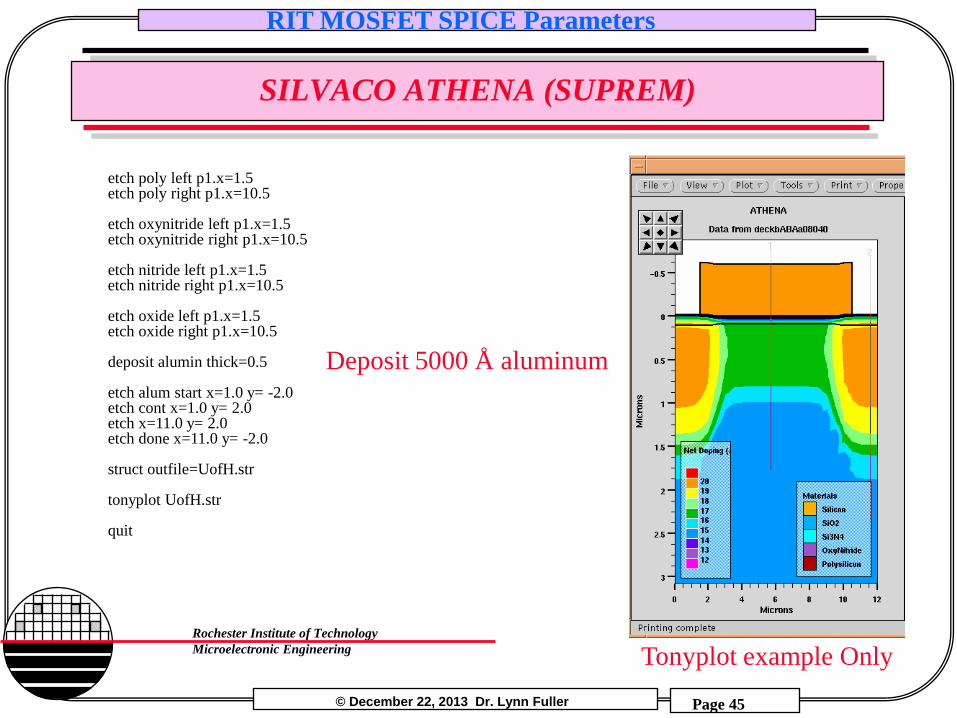
SILVACO ATHENA (SUPREM)
etch poly left p1.x=1.5 etch poly right p1.x=10.5 etch oxynitride left p1.x=1.5 etch oxynitride right p1.x=10.5 etch nitride left p1.x=1.5 etch nitride right p1.x=10.5 etch oxide left p1.x=1.5 etch oxide right p1.x=10.5 deposit alumin thick=0.5 etch alum start x=1.0 y= -2.0 etch cont x=1.0 y= 2.0 etch x=11.0 y= 2.0 etch done x=11.0 y= -2.0 struct outfile=UofH.str tonyplot UofH.str quit
Deposit 5000 Å aluminum
Tonyplot example Only
Page 46
© December 22, 2013 Dr. Lynn Fuller
RIT MOSFET SPICE Parameters
Page 46
Rochester Institute of Technology
Microelectronic Engineering
SILVACO ATHENA (SUPREM)
Channel Doping Profile 1 Crossection of MOSFET
1
2 x
y y
Ch
an
nel
Im
pla
nt
Dose
= 0
Page 47
© December 22, 2013 Dr. Lynn Fuller
RIT MOSFET SPICE Parameters
Page 47
Rochester Institute of Technology
Microelectronic Engineering
SILVACO ATHENA (SUPREM)
Channel Doping Profile 3 D/S Doping Profile 2
y y
Ch
an
nel
Im
pla
nt
Dose
= 0
Page 48
© December 22, 2013 Dr. Lynn Fuller
RIT MOSFET SPICE Parameters
Page 48
Rochester Institute of Technology
Microelectronic Engineering
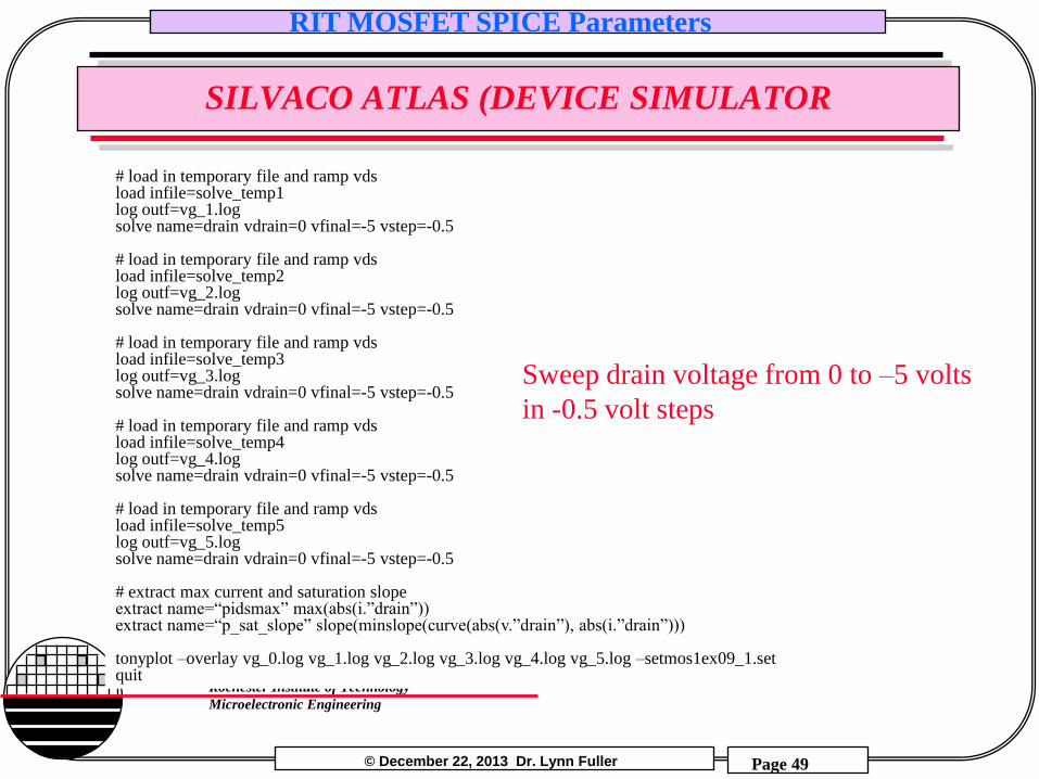
SILVACO ATLAS (DEVICE SIMULATOR)
Go athena Init infile=UofH.str #name the electrodes… Electrode name=gate x=6 Electrode name=source x=0 Electrode name=drain x=12 Electrode name=substrate backside Extract name=“vt” 1dvt ptype qss=1e11 workfunc=5.1 x.val=6 Go atlas # define the gate workfunction Contact name=gate p.poly # define the Gate qss Interface qf=1e11 # use the cvt mobility model for MOS Models cvt srh # set gate biases with Vds=0.0 Solve init Solve vgate=0 vsubstrate=0 outf=solve_temp0 Solve vgate=-1 vsubstrate=0 outf=solve_temp1 Solve vgate=-1 vsubstrate=0 outf=solve_temp2 Solve vgate=-3 vsubstrate=0 outf=solve_temp3 Solve vgate=-4 vsubstrate=0 outf=solve_temp4 Solve vgate=-5 vsubstrate=0 outf=solve_temp5 # load in temporary file and ramp Vds Load infile=solve_temp0 Log outf=Vg_0.log Solve name=drain vdrain=0 vfinal=-5 vstep=-0.5
Read in structure file created by Athena
Define location of gate, source, drain and substrate
Do calculations for given gate voltage and substrate voltage (Vg=0,-1,-2,-3,-4,-5 and Vsub=0,+5,+10+15)
Sweep drain voltage from 0 to –5 volts In –0.5 volt steps
Page 49
© December 22, 2013 Dr. Lynn Fuller
RIT MOSFET SPICE Parameters
Page 49
Rochester Institute of Technology
Microelectronic Engineering
SILVACO ATLAS (DEVICE SIMULATOR
# load in temporary file and ramp vds load infile=solve_temp1 log outf=vg_1.log solve name=drain vdrain=0 vfinal=-5 vstep=-0.5 # load in temporary file and ramp vds load infile=solve_temp2 log outf=vg_2.log solve name=drain vdrain=0 vfinal=-5 vstep=-0.5 # load in temporary file and ramp vds load infile=solve_temp3 log outf=vg_3.log solve name=drain vdrain=0 vfinal=-5 vstep=-0.5 # load in temporary file and ramp vds load infile=solve_temp4 log outf=vg_4.log solve name=drain vdrain=0 vfinal=-5 vstep=-0.5 # load in temporary file and ramp vds load infile=solve_temp5 log outf=vg_5.log solve name=drain vdrain=0 vfinal=-5 vstep=-0.5 # extract max current and saturation slope extract name=“pidsmax” max(abs(i.”drain”)) extract name=“p_sat_slope” slope(minslope(curve(abs(v.”drain”), abs(i.”drain”))) tonyplot –overlay vg_0.log vg_1.log vg_2.log vg_3.log vg_4.log vg_5.log –setmos1ex09_1.set quit
Sweep drain voltage from 0 to –5 volts
in -0.5 volt steps
Page 50
© December 22, 2013 Dr. Lynn Fuller
RIT MOSFET SPICE Parameters
Page 50
Rochester Institute of Technology
Microelectronic Engineering
ATLAS SIMULATED FAMILY OF CURVES
Channel Implant
Dose = none
Vsub = 0
Vgs = -5
-2 -1
-3
-4
Page 51
© December 22, 2013 Dr. Lynn Fuller
RIT MOSFET SPICE Parameters
Page 51
Rochester Institute of Technology
Microelectronic Engineering
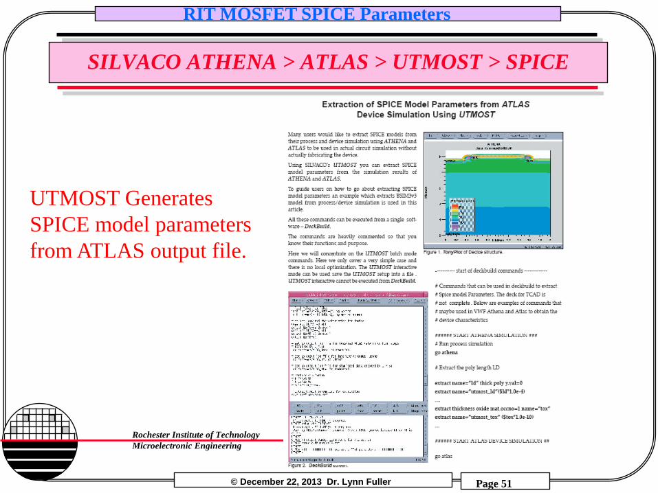
SILVACO ATHENA > ATLAS > UTMOST > SPICE
UTMOST Generates
SPICE model parameters
from ATLAS output file.
Page 52
© December 22, 2013 Dr. Lynn Fuller
RIT MOSFET SPICE Parameters
Page 52
Rochester Institute of Technology
Microelectronic Engineering
SILVACO ATHENA GENERATED IMPURITY PROFILES
Page 53
© December 22, 2013 Dr. Lynn Fuller
RIT MOSFET SPICE Parameters
Page 53
Rochester Institute of Technology
Microelectronic Engineering
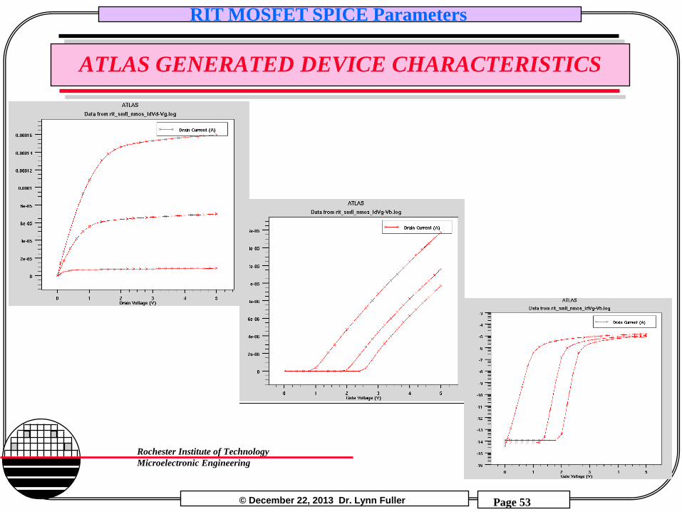
ATLAS GENERATED DEVICE CHARACTERISTICS
Page 54
© December 22, 2013 Dr. Lynn Fuller
RIT MOSFET SPICE Parameters
Page 54
Rochester Institute of Technology
Microelectronic Engineering
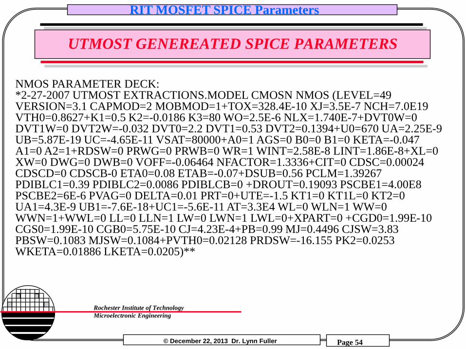
UTMOST GENEREATED SPICE PARAMETERS
NMOS PARAMETER DECK: *2-27-2007 UTMOST EXTRACTIONS.MODEL CMOSN NMOS (LEVEL=49 VERSION=3.1 CAPMOD=2 MOBMOD=1+TOX=328.4E-10 XJ=3.5E-7 NCH=7.0E19 VTH0=0.8627+K1=0.5 K2=-0.0186 K3=80 WO=2.5E-6 NLX=1.740E-7+DVT0W=0 DVT1W=0 DVT2W=-0.032 DVT0=2.2 DVT1=0.53 DVT2=0.1394+U0=670 UA=2.25E-9 UB=5.87E-19 UC=-4.65E-11 VSAT=80000+A0=1 AGS=0 B0=0 B1=0 KETA=-0.047 A1=0 A2=1+RDSW=0 PRWG=0 PRWB=0 WR=1 WINT=2.58E-8 LINT=1.86E-8+XL=0 XW=0 DWG=0 DWB=0 VOFF=-0.06464 NFACTOR=1.3336+CIT=0 CDSC=0.00024 CDSCD=0 CDSCB-0 ETA0=0.08 ETAB=-0.07+DSUB=0.56 PCLM=1.39267 PDIBLC1=0.39 PDIBLC2=0.0086 PDIBLCB=0 +DROUT=0.19093 PSCBE1=4.00E8 PSCBE2=6E-6 PVAG=0 DELTA=0.01 PRT=0+UTE=-1.5 KT1=0 KT1L=0 KT2=0 UA1=4.3E-9 UB1=-7.6E-18+UC1=-5.6E-11 AT=3.3E4 WL=0 WLN=1 WW=0 WWN=1+WWL=0 LL=0 LLN=1 LW=0 LWN=1 LWL=0+XPART=0 +CGD0=1.99E-10 CGS0=1.99E-10 CGB0=5.75E-10 CJ=4.23E-4+PB=0.99 MJ=0.4496 CJSW=3.83 PBSW=0.1083 MJSW=0.1084+PVTH0=0.02128 PRDSW=-16.155 PK2=0.0253 WKETA=0.01886 LKETA=0.0205)**
Page 55
© December 22, 2013 Dr. Lynn Fuller
RIT MOSFET SPICE Parameters
Page 55
Rochester Institute of Technology
Microelectronic Engineering
UTMOST GENEREATED SPICE PARAMETERS FROM ATHENA SIMULATED DEVICE CHARACTERISTICS
PMOS PARAMETER DECK: *2-27-2007 UTMOST EXTRACTIONS.MODEL CMOSP PMOS (LEVEL=49 VERSION=3.1 CAPMOD=2 MOBMOD=1+TOX=328.7E-10 XJ=3.5E-7 NCH=3.0E19 VTH0=-0.6322+K1=0.6423 K2=-0.0856046 K3=80 K3B=0 WO=2.0E-6 NLX=1.0E-7+DVT0W=0 DVT1W=0 DVT2W=-0.032 DVT0=1.5 DVT1=0.50 DVT2=-0.0193+U0=187.362 UA=1.1762E-9 UB=1.0E-22 UC=5.003E-3 VSAT=4.835E6+A0=3.9669 AGS=0 B0=0 B1=0 KETA=-0.0385 A1=0.19469 A2=0.40150+RDSW=0 PRWG=0 PRWB=0 WR=1 WINT=1.67E-8 LINT=3.150E-7+XL=0 XW=0 DWG=0 DWB=0 VOFF=-0.06464 NFACTOR=1.3336+CIT=0 CDSC=0.00024 CDSCD=0 CDSCB=0 ETA0=0.08 ETAB=-0.07+DSUB=0.56 PCLM=1.39267 PDIBLC1=0 PDIBLC2=1E-5 PDIBLCB=0 +DROUT=0.19093 PSCBE1=4E8 PSCBE2=6E-6 PVAG=0 DELTA=0.01 PRT=0+UTE=-1.5 KT1=0 KT1L=0 KT2=0 UA1=4.3E-9 UB1=-7.6E-18+UC1=-5.6E-11 AT=3.3E4 WL=0 WLN=1 WW=0 WWN=1+WWL=0 LL=0 LLN=1 LW=0 LWN=1 LWL=0+XPART=0 +CGD0=2.4E-10 CGS0=2.4E-10 CGB0=5.75E-10 CJ=7.27E-4+PB=0.97 MJ=0.496 CJSW=3.115 PBSW=0.99 MJSW=0.2654+PVTH0=0.00942 PRDSW=-231.3 PK2=1.397 WKETA=1.863 LKETA=5.729)*
Page 56
© December 22, 2013 Dr. Lynn Fuller
RIT MOSFET SPICE Parameters
Page 56
Rochester Institute of Technology
Microelectronic Engineering
UTMOST GENERATED SPICE DECK FROM MEASURED SMFL CMOS PROCESS DEVICE CHARACTERISTICS
*1-15-2007 FROM ROB SAXER UTMOST EXTRACTIONS
.MODEL RITSMFLN49 NMOS (LEVEL=49 VERSION=3.1 CAPMOD=2 MOBMOD=1
+TOX=310E-10 XJ=9.0E-7 NCH=8.2E16 VTH0=1.026
+K1=1.724 K2=-0.1212 K3=0 K3B=0 WO=2.5E-6 NLX=4.80E-9
+DVT0W=0 DVT1W=0 DVT2W=-0.032 DVT0=0.1466 DVT1=0.038 DVT2=0.1394
+U0=687.22 UA=2.34E-9 UB=-1.85E-18 UC=-1.29E-11 VSAT=1.64E5
+A0=0.4453 AGS=0 B0=0 B1=0 KETA=-0.0569 A1=0 A2=1
+RDSW=376.9 PRWG=0 PRWB=0 WR=1 WINT=2.58E-8 LINT=1.86E-8
+XL=0 XW=0 DWG=0 DWB=0 VOFF=-0.1056 NFACTOR=0.8025
+CIT=0 CDSC=-2.59E-5 CDSCD=0 CDSCB-0 ETA0=0 ETAB=0
+DSUB=0.0117 PCLM=0.6184 PDIBLC1=0.0251 PDIBLC2=0.00202 PDIBLCB=0
+DROUT=0.0772 PSCBE1=2.77E9 PSCBE2=3.11E-8 PVAG=0 DELTA=0.01 PRT=0
+UTE=-1.5 KT1=0 KT1L=0 KT2=0 UA1=4.3E-9 UB1=-7.6E-18
+UC1=-5.6E-11 AT=3.3E4 WL=0 WLN=1 WW=0 WWN=1
+WWL=0 LL=0 LLN=1 LW=0 LWN=1 LWL=0
+XPART=0 +CGD0=1.99E-10 CGS0=1.99E-10 CGB0=5.75E-10 CJ=4.23E-4
+PB=0.99 MJ=0.4496 CJSW=3.83 PBSW=0.1083 MJSW=0.1084
+PVTH0=0.02128 PRDSW=-16.155 PK2=0.0253 WKETA=0.01886 LKETA=0.0205)
Page 57
© December 22, 2013 Dr. Lynn Fuller
RIT MOSFET SPICE Parameters
Page 57
Rochester Institute of Technology
Microelectronic Engineering
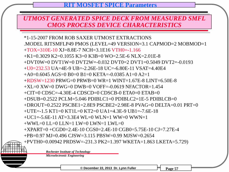
UTMOST GENERATED SPICE DECK FROM MEASURED SMFL CMOS PROCESS DEVICE CHARACTERISTICS
*1-15-2007 FROM ROB SAXER UTMOST EXTRACTIONS
.MODEL RITSMFLP49 PMOS (LEVEL=49 VERSION=3.1 CAPMOD=2 MOBMOD=1
+TOX=310E-10 XJ=8.8E-7 NCH=3.1E16 VTH0=-1.166
+K1=0.3029 K2=0.1055 K3=0 K3B=0 WO=2.5E-6 NLX=2.01E-8
+DVT0W=0 DVT1W=0 DVT2W=-0.032 DVT0=2 DVT1=0.5049 DVT2=-0.0193
+U0=232.53 UA=4E-9 UB=-2.26E-18 UC=-6.80E-11 VSAT=4.40E4
+A0=0.6045 AGS=0 B0=0 B1=0 KETA=-0.0385 A1=0 A2=1
+RDSW=1230 PRWG=0 PRWB=0 WR=1 WINT=1.67E-8 LINT=6.50E-8
+XL=0 XW=0 DWG=0 DWB=0 VOFF=-0.0619 NFACTOR=1.454
+CIT=0 CDSC=-4.30E-4 CDSCD=0 CDSCB-0 ETA0=0 ETAB=0
+DSUB=0.2522 PCLM=5.046 PDIBLC1=0 PDIBLC2=1E-5 PDIBLCB=0
+DROUT=0.2522 PSCBE1=2.8E9 PSCBE2=2.98E-8 PVAG=0 DELTA=0.01 PRT=0
+UTE=-1.5 KT1=0 KT1L=0 KT2=0 UA1=4.3E-9 UB1=-7.6E-18
+UC1=-5.6E-11 AT=3.3E4 WL=0 WLN=1 WW=0 WWN=1
+WWL=0 LL=0 LLN=1 LW=0 LWN=1 LWL=0
+XPART=0 +CGD0=2.4E-10 CGS0=2.4E-10 CGB0=5.75E-10 CJ=7.27E-4
+PB=0.97 MJ=0.496 CJSW=3.115 PBSW=0.99 MJSW=0.2654
+PVTH0=0.00942 PRDSW=-231.3 PK2=1.397 WKETA=1.863 LKETA=5.729)
Page 58
© December 22, 2013 Dr. Lynn Fuller
RIT MOSFET SPICE Parameters
Page 58
Rochester Institute of Technology
Microelectronic Engineering
SMFL CMOS PROCESS “HOT & COLD” SPICE MODELS
All parameters the same except those listed are changed to give more transistor current for the hot models: .model hot nmos ( LEVEL = 11 VERSION = 3.1 TOX = 2.70E-8 VTH0= 0.926 U0 = 750 RDSW = 330) .model hot pmos ( LEVEL = 11 VERSION = 3.1 TOX = 2.70E-8 VTH0= -1.066 U0 = 250 RDSW = 1.00E3) .model cold nmos ( LEVEL = 11 VERSION = 3.1 TOX = 3.50E-8 VTH0= 1.126 U0 = 620 RDSW = 410) .model cold pmos ( LEVEL = 11 VERSION = 3.1 TOX = 3.50E-8 VTH0= -1.266 U0 = 200 RDSW = 1.45E3)
Page 59
© December 22, 2013 Dr. Lynn Fuller
RIT MOSFET SPICE Parameters
Page 59
Rochester Institute of Technology
Microelectronic Engineering
REFERENCES
1. MOSFET Modeling with SPICE, Daniel Foty, 1997, Prentice Hall, ISBN-0-13-227935-5 2. Operation and Modeling of the MOS Transistor, 2nd Edition, Yannis Tsividis,
1999, McGraw-Hill, ISBN-0-07-065523-5 3. UTMOST III Modeling Manual-Vol.1. Ch. 5. From Silvaco International.
4. ATHENA USERS Manual, From Silvaco International.
5. ATLAS USERS Manual, From Silvaco International.
6. Device Electronics for Integrated Circuits, Richard Muller and Theodore
Kamins, with Mansun Chan, 3rd Edition, John Wiley, 2003, ISBN 0-471-59398-2
7. ICCAP Manual, Hewlet Packard
Page 60
© December 22, 2013 Dr. Lynn Fuller
RIT MOSFET SPICE Parameters
Page 60
Rochester Institute of Technology
Microelectronic Engineering
HOMEWORK – SPICE MOSFET MODELS
1. Write an abstract that summarizes the main ideas presented in this document.