Spin-dependent Klein tunneling in graphene: Role of Rashba spin-orbit coupling
Ming-Hao Liu (���), Jan Bundesmann, and Klaus RichterInstitut fur Theoretische Physik, Universitat Regensburg, D-93040 Regensburg, Germany
(Received 2 December 2011; revised manuscript received 12 January 2012; published 3 February 2012)
Within an effective Dirac theory the low-energy dispersions of monolayer graphene in the presence of Rashbaspin-orbit coupling and spin-degenerate bilayer graphene are described by formally identical expressions. Weexplore implications of this correspondence for transport by choosing chiral tunneling through pn and pnpjunctions as a concrete example. A real-space Green’s function formalism based on a tight-binding model isadopted to perform the ballistic transport calculations, which cover and confirm previous theoretical results basedon the Dirac theory. Chiral tunneling in monolayer graphene in the presence of Rashba coupling is shown toindeed behave like in bilayer graphene. Combined effects of a forbidden normal transmission and spin separationare observed within the single-band n ↔ p transmission regime. The former comes from real-spin conservation,in analogy with pseudospin conservation in bilayer graphene, while the latter arises from the intrinsic spin-Hallmechanism of the Rashba coupling.
After the first successful isolation of monolayer graphene(MLG) was announced,1 intriguing properties based on itslow-energy excitation that mimics massless, gapless, and chiralDirac fermions were intensively investigated.2,3 Spin-orbitcoupling (SOC), on the other hand, is the key ingredientof semiconductor spintronics4,5 that was undergoing a rapiddevelopment before the rise of graphene.6 The question aboutthe role of SOC effects in graphene then naturally emerged,including the proposal of graphene as a topological insulator,7
which attracted the attention of various first-principles-basedstudies.8–10
SOC in MLG includes an intrinsic and an extrinsic term.The former reflects the inherent asymmetry of electronhopping between next nearest neighbors7 (i.e., a generalizationof Haldane’s model11). The latter is induced by the electricfield perpendicular to the graphene plane, which can beexternally controlled, and resembles the Rashba model12,13
for the two-dimensional electron gas. Agreement has beenachieved, based on first-principles calculations,9,10 that theintrinsic SOC term opens a gap of the order of 2λI ≈ 24 μeV,while the Rashba SOC removes the spin degeneracy andcreates a spin-splitting 2λR at the K and K ′ points that hasa linear dependence on an external electric field E with theslope of about 100 μeV per V/A of E. Under a strong gatevoltage, the Rashba coupling may in principle dominate theintrinsic SOC in MLG.9,10
The low-energy spectrum of MLG plus the Rashba coupling(MLG + R) was derived by Rashba,14 based on the Kane-Melemodel7 (i.e., an effective Dirac Hamiltonian). An earlier workby one of us15 started with a tight-binding model (TBM) andobtained an equivalent form of the low-energy expansion,16
EMLG+R(q) ≈ μ 12 [
√(3tR)2 + (3ta · q)2 + ν(3tR)], (1)
which also agrees with expressions given in Refs. 9 and 10when λI = 0. Here μ,ν = ±1 are band indices, t and tR arenearest-neighbor kinetic and Rashba hopping parameters, re-spectively, a ≈ 1.42A is the bonding length, and q = K + δk
with |δk|a � 1. Recall for comparison the low-energy spec-trum of bilayer graphene (BLG),2,17
EBLG(q) ≈ μ 12
(√γ 2
1 + (3ta · q)2 + νγ1), (2)
where γ1 is the nearest-neighbor hopping between the twographene layers. Note that the next nearest-neighbor interlayerhoppings γ3 and γ4 do not influence the band dispersion nearK . The completely different mechanisms of (i) pseudospincoupling between carriers from the two graphene layers ofBLG through interlayer hopping γ1 and (ii) real-spin couplingbetween up and down spins within MLG through Rashbahopping tR happen to lead to an identical mathematical form inEqs. (1) and (2) that can be clearly mapped onto each other18,19
with γ1 ↔ 3tR as sketched in Fig. 1. This unambiguouslyimplies that low-energy physics in MLG + R and BLG shouldbehave similarly.
In this paper we tackle the question of whether the transportin MLG + R behaves as in BLG by choosing the issue ofKlein tunneling2,3,20,21 (or, in general, chiral tunneling) asa concrete example. Chiral tunneling in graphene has beenshown to exhibit completely different behavior in MLG andBLG based on the Dirac theory.22 Tunneling at normal inci-dence in MLG shows a suppression of backscattering, whichresembles the original Klein paradox in relativistic quantumelectrodynamics23 and hence the name Klein tunneling, whilein BLG it shows a perfect reflection, which is strictly speakinga consequence of forbidden interband transition also due to the
γ1
tRγ1 3tR
K (K )
FIG. 1. (Color online) Schematic of the pseudospin couplingthrough γ1 in BLG (left panel) and real-spin coupling through tRin MLG (right), which lead to an identical low-energy dispersionnear K and K ′.
MING-HAO LIU, JAN BUNDESMANN, AND KLAUS RICHTER PHYSICAL REVIEW B 85, 085406 (2012)
chiral nature of graphene. The theoretical discussion of chiraltunneling so far focuses mainly on spin-independent tunnelingthrough pn and pnp junctions,21,22,24–30 while SOC effectsare less discussed.18,31–33 In addition, the relevant theoreticalunderstanding so far is based on Dirac theory, which is validonly for the Fermi level close to the charge neutrality point andallows one only to consider certain relatively simple systems.A recent study discussing the interplay between the Aharanov-Bohm effect and Klein tunneling in graphene, started with aTBM,34 but the nanoribbon type of the leads used in that workmay have edge effects included that can be very different fromthe bulk properties of graphene. A more transparent theoreticalstudy of chiral tunneling in graphene directly bridging theanalytical Dirac theory and the numerical TBM computationis so far missing and deserves consideration.
In the present work, we re-treat this issue of chiraltunneling in graphene based on the TBM and show a unifieddescription, allowing for a broad range of geometries andcomplementing the existing results based on the Dirac theory.Straightforward generalization to the case of MLG + R revealsa spin-dependent tunneling behavior in close analogy withthat in BLG, with the role of pseudospin in BLG replacedby real spin in MLG + R. Specifically, a combined behaviorof spin-Hall-based spin separation and suppression of normaltransmission will be shown.
This paper is organized as follows. In Sec. II we brieflysummarize the theoretical formalism applied in the presentcalculation, namely, real-space Green’s function formalismin noninteracting bulk graphene. In Sec. III we show ourTBM results including the consistency with the Dirac theory, adirect comparison between BLG and MLG + R, and a deeperdiscussion of the MLG + R case. We review also briefly therecent experimental progress on the Rashba spin splitting andKlein tunneling in graphene in Sec. IV, and finally concludein Sec. V.
II. FORMALISM
A. Tight-binding model for “bulk” graphene
We choose the TBM for describing the electronic propertiesof graphene, which is a well established way to treat graphenenumerically. For spin-degenerate MLG, the Hamiltonian reads
HMLG =∑
i
Vic†i ci − t
∑〈i,j〉
c†i cj , (3)
where the operator c†i (ci) creates (annihilates) an electron at
site i (including both sublattices A and B). The first sum inEq. (3) runs over all the atomic sites in the considered regionwith on-site potential Vi , and the second sum runs over allthe pairs of neighboring atomic orbitals 〈i,j 〉 with kinetichopping parameter t (≈3 eV). The next nearest neighborkinetic hopping term, usually characterized by t ′ ≈ 0.1t , canbe added in Eq. (3) but will not be considered in the presentwork due to the minor role it plays in the bulk transportproperties for low-energy excitation.
Spin-orbit interactions can be incorporated into the TBMby altering the spin-dependent hopping between nearest andnext-nearest neighbors,7,35 modifying Eq. (3) as
HMLG+R =∑
i
Viσ0c
†i ci +
∑〈i,j〉
c†i [−tσ 0 + itR(�σ × dij )z]cj .
(4)
Here σ 0 is the 2 × 2 identity matrix, tR is the Rashba spin-orbithopping parameter, dij is the unit vector pointing from site j
to i, and �σ = (σx,σ y,σ z) is the vector of (real-) spin Paulimatrices. We take into account only the extrinsic SOC andneglect the intrinsic term in order to highlight the role of theRashba SOC.
For spin-degenerate BLG, we consider
HBLG =∑
m=1,2
H(m)MLG − γ1
∑j
(b†2,j a1,j + H.c.), (5)
where H(m)MLG is HMLG given by Eq. (3) of the mth graphene
layer, am,j (bm,j ) annihilates an electron on sublattice A
(B) in layer m = 1,2 at unit cell j (that contains twosublattice sites belonging to A and B), and the interlayercoupling strength γ1 ≈ 0.4 eV corresponds to the nearestneighbor hopping between the two MLG layers. Furtherinterlayer hopping terms,2 −γ4
∑j (a†
2,j a1,j + b†2,j b1,j+ H.c.)
and −γ3∑
j (a†2,j b1,j+ H.c.), are not considered in the present
calculation, since they do not influence the low-energy exci-tation. Throughout the presentation of the numerical resultsin Sec. III, the kinetic hopping parameters will be fixed att = 3 eV and γ1 = 0.39 eV, while the value of the Rashbahopping parameter tR depends on the context.
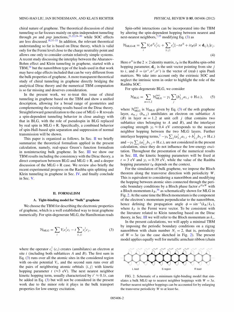
For the simulation of bulk graphene, we impose the Blochtheorem along the transverse direction with periodicity W .This is equivalent to considering a nanoribbon and modifyingthe hopping between atomic sites connected through the peri-odic boundary conditions by a Bloch phase factor eikBW witha Bloch momentum kB ,36 as schematically shown for MLG inFig. 2. At the same time the Bloch momentum is the componentof the electron’s momentum perpendicular to the nanoribbon,hence defining the propagation angle φ = sin−1(kB/kF ),where kF is the Fermi wave vector. To be consistent withthe literature related to Klein tunneling based on the Diractheory, in Sec. III we will refer to the Bloch momentum as ky .
In the present calculations, we will apply a minimal TBMby imposing the periodic boundary conditions on a zigzagnanoribbon with chain number Nz = 2, that is, periodicityof W = 3a (as the case sketched in Fig. 2). The presentmodel applies equally well for metallic armchair ribbon (chain
eikyW eikyW eikyW
· · ·
L lead
eikyWeikyWeikyW
· · ·
R lead
eikyW eikyW eikyW eikyW eikyW
S region
FIG. 2. Schematic of a minimum tight-binding model that sim-ulates a bulk MLG up to nearest neighbor hoppings with W = 3a.Further nearest neighbor hoppings can be accounted for by enlargingthe transverse periodicity W to at least 6a.
085406-2
SPIN-DEPENDENT KLEIN TUNNELING IN GRAPHENE: . . . PHYSICAL REVIEW B 85, 085406 (2012)
number Na being a multiple of 3) with periodic boundaryconditions, but the minimal model would require Na = 3 (i.e.,periodicity of W = 3
√3a).
B. Brief summary of real-space Green’s function formalism
We consider open systems connected to the outer world bytwo leads (see Fig. 2). According to the real-space Green’sfunction formalism37 we numerically calculate the Green’sfunctions of our system,
Gr/a
S = [E − HS − �r/a ± iη]−1, (6)
where the self-energies of the leads (�r/a = �r/a
L + �r/a
R )reflect the fact that our system is open. The powerful recipeconstructed in Ref. 36 for graphene handles a lead as a semi-infinite repetition of unit cells and allows for incorporatingany kind of lattice structure and one-body interaction such asSOCs. The transmission probability for an electron travelingfrom lead L to lead R is given by the Fisher-Lee relation,36,37
TRL = Tr(LGr
SRF aS
), (7)
where the trace is done with respect to the lattice sites.The spectral matrix functions L/R are given by the leadself-energies as L/R = i(�r
L/R − �aL/R).
For a given Bloch momentum ky and a given Fermi energyEF [subject to a Fermi wave vector kF via Eq. (1) for MLG + Ror Eq. (2) for BLG], the incoming propagation angle φ ofthe electron wave can be defined as φ = sin−1(ky/kF ). Theangle-dependent transmission function T (φ) is obtained fromEq. (7), which can be generalized to a spin-resolved version.38
III. TRANSPORT RESULTS
In this section we present numerical results of our tight-binding transport calculations. We first show the consistency ofour tight-binding calculations with the existing effective Diractheory in Sec. III A. A direct comparison between BLG andMLG + R will then be shown in Sec. III B. Finally, Sec. III Cis devoted to MLG + R for pn junctions, in particular the roleof Rashba SOC for chiral tunneling.
A. Consistency with Dirac theory
We first consider tunneling in graphene without SOC andconfirm existing results, limited to low-energy excitations,by our tight-binding calculations. We pick two pioneeringtheoretical works to demonstrate the consistency explicitly.Consistency with recent works of tunneling in grapheneheterojunctions in the presence of SOC18,31 has also beenchecked, but is not explicitly shown here.
1. Chiral tunneling in MLG vs BLG
Tunneling in MLG and BLG behaves quite differently asmentioned in Sec. I and pointed out by Katsnelson et al.22
For a quantitative comparison we consider a barrier of widthD = 100 nm and the incoming Fermi wave vector kF =2π/50 nm−1 as in Ref. 22 for both MLG and BLG [seeFigs. 3(a) and 3(c)]. Note that in order to exactly match thebarrier width, we set the bonding length a = (4
√3)−1nm,
which differs from the realistic value of about 1.42 A by
EF
D
V0
V (x)
k
top view
|k| = kF
kyφ
(a)
1 12 20 −90°
−60°
−30°0°
30°
60°
90°
(b)
γ1
EF
D
V0
V (x)
k
(c)
1 12 20 −90°
−60°
−30°0°
30°
60°
90°
(d)
FIG. 3. (Color online) Tunneling through a barrier for (a), (b)MLG with EF = 3takF /2 = 81.6 meV and (c), (d) BLG with EF =(3takF /2)2/γ1 = 17.1 meV. In (b), red (light gray) and blue (darkgray) curves correspond to V0 = 196.8 meV and V0 = 280.3 meV,respectively. In (d), red (light gray) and blue (dark gray) curvescorrespond to V0 = 48.7 meV and V0 = 100.7 meV, respectively.In both cases the barrier width is D = 100 nm and the incomingFermi wave vector is kF = 2π/50 nm−1, as considered in Ref. 22.
only less than 2%, so that the number of hexagons used hereamounts to D/(
√3a) = 4 × [D]nm = 400.
The resulting transmission probabilities as a function ofthe incident angle φ are depicted in Figs. 3(b) and 3(d). Theyreproduce the results of Fig. 2 in Ref. 22 almost perfectly,if we choose slightly different EF and V0, to which thetransmissions at finite angles are sensitive. The remaining tinydifference between our TBM results and their Dirac theoryresults39 simply reflects the basic difference between the twoapproaches: For graphene the effective Dirac theory is validonly for energies close to the Dirac point, while the TBM issuitable for the entire energy range.
Note that the maximal values of the transmission functionsin Fig. 3 are 2, since the valley degeneracy is automaticallyincorporated in the tight-binding formalism. Later when wetake spin also into account, the maximum of the transmissionfunction will be 4. The transmission probabilities calculatedby the Dirac theory always have their maximum of 1 due to thenormalized incoming wave, unless a proper degeneracy factoris taken into account.
2. Klein tunneling in MLG: Sharp vs smooth interface
Tunneling in MLG through a pn junction exhibits proba-bility one at normal incidence and is called Klein tunneling.In experiments, a graphene pn junction can be realized byusing a backgate, which tunes the carrier density (and hencethe Fermi level) globally, and a topgate that tunes locally thecarrier density, equivalent to the potential step V0 at the otherside.40 The carrier densities on the two sides can be controlledto be of opposite signs, forming the pn junction. In between,however, the variation of the carrier density is never abruptin reality. Cheianov and Fal’ko showed, based on the Diractheory, that the interface of the pn junction actually matters.24
They considered symmetric pn junctions (i.e., V0 = 2EF ) with
085406-3
MING-HAO LIU, JAN BUNDESMANN, AND KLAUS RICHTER PHYSICAL REVIEW B 85, 085406 (2012)
EF V0
V (x)
k
−90 −60 −30 0 30 60 900
0.5
1
1.5
2
φ (deg)
T(φ
)
Eq. (8)TBM
(a)
EF
d
V0
V (x)
k
−90 −60 −30 0 30 60 900
0.5
1
1.5
2
φ (deg)
T(φ
)
d = 20 nm
(b)
FIG. 4. (Color online) Klein tunneling in MLG through a pnjunction with a (a) sharp and (b) smooth interface. (a) Comparisonbetween TBM (dashed line) and Eq. (8) [solid green (gray)] showingperfect agreement (EF = 80 meV). (b) Comparison between TBM(long and short dashed) and Eq. (11) [solid green (light gray) andred (dark gray)] for kF d ≈ 6.16 (EF = 200 meV) and kF d ≈ 1.54(EF = 50 meV), respectively.
sharp and linearly smooth interfaces, which we briefly reviewand compare with our TBM results in the following.
a. Sharp interface. For a symmetric pn junction with asharp interface [see the schematic in Fig. 4(a)], the transmis-sion probability as a function of φ was written as24
T (φ) = cos2 φ, (8)
which does not depend on the potential step height. Thissurprisingly simple expression matches our TBM result alwaysperfectly as long as V0 = 2EF , as shown in Fig. 4(a).
For a step potential with arbitrary height V0 = 2EF , thetransmission probability as a function of the incident angle φ
and the outgoing angle θ can be derived as
T (φ,θ ) = 2 cos φ cos θ
1 + cos(φ + θ ), (9)
which agrees with our TBM calculation equally well as thesymmetric case (not shown). The two angles φ and θ areconnected to each other due to conservation of transversemomentum by
sin θ = s|EF |
|EF − V0| sin φ, (10)
where s = +1 for nn′ or pp′ and −1 for np or pn. Equation (9)clearly recovers the symmetric pn junction case of Eq. (8)when choosing s = −1 and V0 = 2EF in Eq. (10). Note thatin the case of |EF − V0| < |EF |, the Fermi wave vector in theoutgoing region is shorter than that in the incoming region,and an additional constraint for φ has to be applied to ensure| sin θ | � 1 [i.e., φ � |φc| with φc = sin−1(|EF − V0|/|EF |)].
Previously it has been stated that the single-valley Diracpicture, based on which Eqs. (8) and (9) are derived, isnot equivalent to the TBM.41 The difference in their work,however, becomes noticeable only when the distance betweenone of the involved energies and the Dirac point exceedsroughly 300 meV. In our simulation, indeed the deviation forthe symmetric pn junction case with, say EF = 300 meV,is less than 0.5%. The agreement of our TBM and the Dirac
theory therefore confirms that the intervalley scattering, whichis mainly responsible for the nonequivalence at high energies,is indeed negligible.
b. Smooth interface. For symmetric pn junctions witha linearly varying region of width d [see the schematicin Fig. 4(b)], the analytical derivation for the transmissionprobability within the Dirac theory yields24
T (φ) = exp
(−π
kF d
2sin2 φ
)(11)
for kF d � 1.42 This formula, together with the validitycriterion kF d � 1, are tested by our tight-binding calculationsshown in Fig. 4(b), where two sets of parameters are con-sidered. For kF d ≈ 6.16 we find very good agreement withEq. (11), while the result for kF d ≈ 1.54 exhibits noticeabledeviations from the analytical prediction at large angles |φ|.The smoothing function was assumed in their work as linearbut the reality might be much more complicated, which is thennot accessible by the Dirac theory but again straightforwardby our tight-binding calculation. Nevertheless, the exponentialform of Eq. (11) is still a good description regardless of theactual form of the smoothing function, as we have numericallychecked. What really matters is only the product kF d.
Unlike the sharp pn interface, a compact form of transmis-sion probability for the asymmetric case does not exist so far.
B. pn junction: BLG vs MLG + R
We next show the direct correspondence between BLG andMLG + R by considering exactly the same potential barrierand incident Fermi energy as in Fig. 3(d) for BLG, and set3tR = γ1 = 0.39 eV for MLG + R here. (A discussion withweaker, realistic tR will be continued in the next section.)The total transmission shown in Fig. 5 for MLG + R indeedresembles the curves in Fig. 3(d) for BLG, as expected dueto the identical form of their low-energy dispersions (1)and (2). The most important feature of chiral tunneling inBLG, forbidden normal transmission, now appears also in the
0.4
0.4
0.8
0.8
1.2
1.2
1.6
1.6
2
2
0
−90°−60°
−30°
0°
30°
60°90°
V0 = 48.7 meVV0 = 100.7 meV
0.4
0.4
0.8
0.8
1.2
1.2
1.6
1.6
2
2
0
−90°−60°
−30°
0°
30°
60°90°
T↑ = T↑↑ + T↓↑T↓ = T↓↓ + T↑↓
V0 = 48.7 meV
0.4
0.4
0.8
0.8
1.2
1.2
1.6
1.6
2
2
0
−90°−60°
−30°
0°
30°
60°90°
T↑ = T↑↑ + T↓↑T↓ = T↓↓ + T↑↓
V0 = 100.7 meV
Total T Spin-resolved T↑ and T↓
FIG. 5. (Color online) (a) Angle-resolved total transmission T
for tunneling through a pnp junction in MLG + R with the samebarrier height V0, barrier width D, and Fermi energy EF as used inFig. 3(d) for BLG, and a substitution 3tR = γ1 = 0.39 eV. (b) and(c) show spin-resolved transmission probabilities for V0 = 48.7 meVand V0 = 100.7 meV, respectively.
085406-4
SPIN-DEPENDENT KLEIN TUNNELING IN GRAPHENE: . . . PHYSICAL REVIEW B 85, 085406 (2012)
case of MLG + R. In BLG, T (φ = 0) = 0 was understood asthe consequence of pseudospin conservation. For MLG + R,T (φ = 0) = 0 can be expected as the consequence of real-spinconservation. Indeed, this can be demonstrated by computingthe nonequilibrium local spin density, which can be obtainedfrom the lesser Green’s function,43 considering two cases, 0 <
EF < 3tR and −3tR < EF < 0, both with ky = 0. Within thissingle-band transmission, the local spin densities for positiveand negative EF point to opposite directions, indicating thatnormal incidence transmission between n and p regions willbe forbidden.
Next we discuss the spin-resolved transmission. The quan-tization axis is chosen as the out-of-plane direction, so thatthe transmission of, for example, T↓↑ means the probability ofan incoming +Sz electron ending up as an outgoing −Sz one.Since the incoming angle dependence φ of the transmissionprobabilities are analyzed, we define T↑ = T↑↑ + T↓↑ as thetransmission ability of the +Sz electron (or ↑ spin), and viceversa. (Alternatively, one can also analyze the outgoing angledependence and define T↑ as T↑↑ + T↑↓, not used here. Eitherway, the total transmission
∑σ,σ ′=↑,↓ Tσσ ′ = T↑ + T↓ = T is
ensured.)The choice of quantization axis z is not necessary but
facilitates relating the present spin-dependent tunneling inMLG with the issue of intrinsic spin-Hall effect previouslydiscussed in semiconductors. The spin-resolved transmissioncurves shown in Fig. 5 exhibit opposite lateral preference ofthe ↑ and ↓ electron spins, which is an intrinsic spin-Hallmechanism due to the Rashba SOC. In a semiconductortwo-dimensional electron gas (i.e., a continuous system ratherthan discrete as in the TBM), such an intrinsic spin-Halldeflection of opposite Sz electrons can be easily explainedby the concept of a spin-orbit force based on the Heisenbergequation of motion,44,45
Fso = m
ih
[1
ih[r,H],H
]= 2mα2
R
h3 (p × ez)σz. (12)
Here H = p2/2m + (αR/h)(pyσx − pxσ
y) is the continuoustwo-dimensional Hamiltonian with Rashba SOC, r and pare the position and momentum operators, αR is the Rashbacoupling parameter (rather than the hopping one, tR), and σ z isthe sign of the Sz spin component. The T↑ and T↓ curves shownin Fig. 5 therefore reveal a combined effect of forbidden normaltransmission due to conservation of real spin and the intrinsicspin-Hall deflection that can be understood by Eq. (12).
A few remarks are due before we move on. To connectBLG with MLG + R we put 3tR = γ1 = 0.39 eV, which isapparently far from reality. In general the Rashba splittinginduced by electrical gating is roughly of or less than the orderof 100 μeV (see Sec. IV). Fermi energy lying within thissplitting, which is also our main interest, projects to a muchshorter Fermi wave vector kF , leading to a much longer d up toa few or a few tens of microns in order for kF d � 1 to be valid.This implies that the influence of the interface on the tunnelingin MLG + R is normally negligible, unless d is that long. Inaddition, tunneling through a pnp junction will also requirea long barrier width D for electrons subject to such a shortkF ; otherwise, the barrier is merely a weak perturbation to theelectron due to its long Fermi wave length. Based on these
EF
−240 −30 60 150 3600
1
2
V0 (μeV)
T
FIG. 6. (Color online) Transmission T at normal incidence (ky =0) as a function of potential step height V0 for tunneling through apn junction in MLG + R. The leftmost solid band diagram above themain panel corresponds to the incoming n side. The five ticks on theV0 axis correspond to the above five dashed band diagrams for theoutgoing side.
remarks, we will focus in the next section only on pn junctionsin MLG + R with a reasonable Rashba hopping parameter.
C. pn junction in MLG + R
In the following we demonstrate in detail the role of RashbaSOC in tunneling through a potential step in MLG + R. TheRashba hopping parameter will be fixed to tR = 30 μeV andthe Fermi energy in most cases to EF = 2tR , which lies withinthe spin-orbit splitting 3tR (see Fig. 1).
1. Normal incidence
We begin with the case of normal incidence, ky = 0.In Sec. III B we have discussed the one-band transmissionselection rule (i.e., n ↔ p transmission is forbidden). Thetransmission from the left side at Fermi energy 0 < EF < 3tRto the right side with potential V0 is expected to be zerowhenever a single-band n → p transmission is attempted.Indeed, as shown in Fig. 6, a zero transmission gap of T
as a function of V0 is found. The gap lies in the intervalof EF < V0 < EF + 3tR , corresponding to the single-bandn → p transmission. Note that contrary to the valley-valveeffect in zigzag nanoribbons,46–48 the gap shown here arisessolely due to a bulk property.
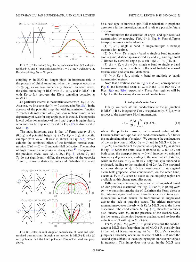
2. Angle- and spin-resolved transmission
We proceed with angle- and spin-resolved transmissionand consider first the trivial case with EF = 0.5 meV wellabove the Rashba splitting 3tR = 90 μeV, as shown in Fig. 7.In this case the maximum of T = T↑ + T↓ is 4 since twospin subbands and two valleys are involved in transport.The total transmission curve resembles the expected cos2 φ
behavior as discussed in Sec. III A 2, showing that the Rashbaeffect plays only a minor role. The spin-resolved T↑ andT↓ curves differ only slightly at |φ| = sin−1(kin
F /koutF ) ≈ 56◦,
where kinF and kout
F are the inner and outer radius of thetwo concentric Fermi circles, respectively. Tunneling in BLGwith EF well above γ1 behaves similarly (i.e., the interlayer
085406-5
MING-HAO LIU, JAN BUNDESMANN, AND KLAUS RICHTER PHYSICAL REVIEW B 85, 085406 (2012)
−90 −60 −30 0 30 60 90
0
1
2
3
4
φ (deg)
T(φ
)
T↑T↓T
L R
EF
V (x)
(EF , tR, V0) = (0.5, 0.03, 1) meV
FIG. 7. (Color online) Angular dependence of total (T ) and spin-resolved (T↑ and T↓) transmissions for EF = 0.5 meV well above theRashba splitting 3tR = 90 μeV.
coupling γ1 in BLG no longer plays an important role inthe process of chiral tunneling when the transport occurs atEF � γ1), as we have numerically checked. In other words,the chiral tunneling in BLG with EF � γ1 and in MLG + Rwith EF � 3tR recovers the Klein tunneling behavior asin MLG.
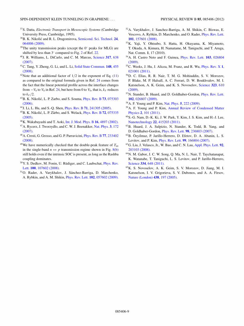
Of particular interest is the nontrivial case with |EF | < 3tR .As a test, we first consider V0 = 0 as shown in Fig. 8(a). In theabsence of the potential step, the total transmission functionT reaches its maximum of 2 (one spin subband times valleydegeneracy of two) for any angle φ, as it should. The oppositelateral deflection tendency of the ↑ and ↓ spins is again clearlyseen and can be explained based on Eq. (12) as discussed inSec. III B.
The most important case is that of Fermi energy EF ∈(0,3tR) and potential height V0 ∈ (EF ,EF + 3tR). A specificexample with V0 = 100 μeV is shown in Fig. 8(b), whichexhibits the combined effect of the forbidden normal trans-mission [T (φ = 0) = 0] and spin-Hall deflection. The numberof high transmission peaks is always two.49 Compared tothe previous trivial case (EF > 3tR; Fig. 7) where T↑ andT↓ do not significantly differ, the separation of the opposite↑ and ↓ spins is distinctly enhanced. Whether this could
0.40.4 0.80.8 1.21.2 1.61.6 22 0 −90°
−60°
−30°
0°
30°
60°
90°
TT↑T↓
L R
EFV (x)
(EF, tR, V0)= (60, 30, 0) μeV
(a)
0.40.4 0.80.8 1.21.2 0 −90°
−60°
−30°
0°
30°
60°
90°
TT↑T↓
L R
EFV (x)
(EF, tR, V 0)= (60, 30, 100) μeV
(b)
FIG. 8. (Color online) Angular dependence of total and spin-resolved transmissions through a pn junction in MLG + R with (a)zero potential and (b) finite potential. Parameters used are givenabove.
be a new type of intrinsic spin-Hall mechanism in graphenedeserves a further investigation, and is left as a possible futuredirection.
We summarize the discussion of angle- and spin-resolvedtransmission by mapping T (φ,V0) in Fig. 9. Four differenttransport regimes can be identified:
(1) V0 < 0, single n band to single/multiple n band(s)transmission regime.
(2) 0 < V0 < EF , single n band to single n band transmis-sion regime; distinct spin-resolved T↑ and T↓, and high totalT limited by a critical angle φc = sin−1(|EF − V0|/|EF |).
(3) EF < V0 < EF + 3tR , single n band to single p bandtransmission regime; combined effects of forbidden normaltransmission and spin-Hall deflection.
(4) V0 > EF + 3tR , single n band to multiple p bandstransmission regime.
Note that a vertical scan in Fig. 9 at φ = 0 corresponds toFig. 6, and horizontal scans at V0 = 0 and V0 = 100 μeV toFigs. 8(a) and 8(b), respectively. These four regimes will behelpful in the following discussion of conductance.
3. Integrated conductance
Finally, we calculate the conductance of the pn junctionin MLG + R by integrating T (φ), or equivalently, T (ky), withrespect to the transverse Bloch momentum,
G = e2/h
2kF
∫ kF
−kF
T (ky)dky, (13)
where the prefactor ensures the maximal value of theLandauer-Buttiker-type ballistic conductance to be e2/h timesthe maximal number of modes.37 We compare the conductanceof the pn junction in MLG (tR = 0) and in MLG + R (tR =30 μeV) as a function of the potential step height V0, as shownin Fig. 10. Since the Fermi level is fixed to EF = 60 μeV forboth cases, the transport for tR = 0 will involve two spin andtwo valley degeneracies, leading to the maximal G of 4e2/h,while in the case of tR = 30 μeV only one spin subband isprojected, leading to the maximal G of 2e2/h. The maximalG occurs always at V0 = 0 that corresponds to an ungatedclean bulk graphene. Zero conductance, on the other hand,occurs at V0 = EF since no states at the outgoing region areavailable at this charge neutrality point.
Different transmission regimes can be distinguished basedon our previous discussion for Fig. 9. For V0 ∈ [0,60] μeV(n → n transmission), the rise of V0 shrinks the Fermi circle atthe outgoing region and hence introduces a critical transversemomentum, outside which the transmission is suppresseddue to the lack of outgoing states. The critical transversemomentum reduces linearly with V0 for MLG due to the lineardispersion. The conductance G, Eq. (13), therefore reducesalso linearly with V0. In the presence of the Rashba SOC,the low-energy dispersion becomes quadratic, and so does thereduction of G with V0 in MLG + R.
For V0 ∈ [60,150] μeV (n → p transmission), the conduc-tance of MLG rises faster than that of MLG + R, possibly dueto the help of Klein tunneling. At V0 = 150 μeV, a suddenjump (or a shoulder) occurs in the case of MLG + R since thesecond spin subband at the outgoing region starts to participatein transport. This jump does not occur in the MLG case
085406-6
SPIN-DEPENDENT KLEIN TUNNELING IN GRAPHENE: . . . PHYSICAL REVIEW B 85, 085406 (2012)
φ (deg)
V0
[μeV
]T
−90 −60 −30 0 30 60 90−60
−30
0
30
60
90
120
150
180
0
1
2
φ (deg)
T↓
−90 −60 −30 0 30 60 90
φ (deg)
T↑
−90 −60 −30 0 30 60 90
= +
FIG. 9. (Color online) Transmission through a pn junction in MLG + R as a function of incident angle φ and potential step height V0.Four transmission regimes can be distinguished: (i) V0 < 0, (ii) 0 < V0 < EF , (iii) EF < V0 < EF + 3tR , and (iv) V0 > EF + 3tR , withEF = 60 μeV and 3tR = 90 μeV.
since both spin subbands are always degenerate. An earlierrelated work based on Dirac theory considered both intrinsicand Rashba SOCs.18 The V0 dependence of G for the Rashbadominated case in that work agrees well with the MLG + Rcurve shown in Fig. 10, including the shoulder.
IV. EXPERIMENTAL ASPECTS
A. Rashba spin splitting in graphene
Whereas the Rashba spin splitting in MLG induced by anapplied electric field is in general in the order of no morethan 100 μeV, which is beyond the present resolution ofangle-resolved photoelectron spectroscopy (ARPES), directexperimental observation of the Rashba spin splitting at K
and K ′ in agreement with the first-principles calculations9,10
is so far not reported. An earlier experiment on epitaxialgraphene layers on a Ni(111) surface reported a large Rashbainteraction50 up to 225 meV but was soon questioned sincethe splitting might simply reveal a Zeeman-type splittingdue to the ferromagnetic nature of nickel.51 An intercalatedAu monolayer between the graphene layer and the Ni(111)substrate reduced the splitting to about 13 meV and wasconcluded as the Rashba effect on the π states supportedby spin-resolved ARPES.52 However, the low-energy bandstructure of MLG + R at that time was not yet clear, anda simplified picture was adopted in the explanation of the
−180 −120 −60 0 60 120 180 240 3000
1
2
3
4
V0 (μeV)
G(e
2/h)
MLG (tR = 0)0
1
20 EF EF + 3tR
MLG+R (tR = 30 μeV)
FIG. 10. (Color online) Integrated conductance of the ballistic pnjunction in MLG with tR = 0 and MLG + R with tR = 30 μeV.
measured spin splitting. In addition, transport properties ofgraphene based on metallic substrates can be difficult to isolatesince a large bulk current will interfere as background.53
Throughout the above calculations we have mostly focusedon a rather weak Rashba hopping parameter tR = 30 μeV,
yielding a splitting at the K and K ′ points 3tR = 90 μeV,which is a realistic and rather conservative estimate for thegate-voltage-induced Rashba SOC strength. A recent proposalof impurity-induced SOC in graphene,54 however, indicatedthat the coupling strength can be strongly enhanced by puttingheavy adatoms55 as well as by hydrogenation.54,56
B. Klein tunneling in MLG
Indirect and direct experimental evidences of Klein tun-neling in MLG have been reported recently.57,58 For detailedreviews, we refer to Refs. 2,3,20,21 and 59. A very recentexperiment on transport through a pn junction in MLG usedan embedded local gate, which yields high quality ballistictransport and perfectly independent control of the local carrierdensity, as well as the feature of Klein tunneling.60
Recall the tR = 0 curve of conductance for MLG shownin Fig. 10. Overall, the conductance for n → n transmissionwith V0 < 0 is always higher than that for n → p transmissionwith V0 > EF . Even though Klein tunneling leads to perfecttransmission at normal incidence in the latter case, the decayof T with incident angle eventually yields a lower conductanceafter integration. This feature has been agreed in recentexperiments for pn and pnp junctions in MLG.40,57,58,60–64 Thedifference of the conductance, or equivalently the resistance,between the nn and np (or between pp and pn) in experimentsis even more obvious possibly due to the smooth interfacethat leads to an exponentially decaying form of T ,24 as wehave reviewed and discussed in Sec. III A 2. In fact, for MLGwe have numerically checked G for pn junctions with asmooth interface, which indeed can enhance the differenceof G between the nn and np regimes.
Another interesting feature so far experimentally reportedonly in Refs. 58 and 60 is the Fabry-Perot oscillation of theconductance for pnp junctions due to the interference betweenthe two interfaces of the central barrier. This feature requiresthe system to be ballistic and can be naturally revealed by our
085406-7
MING-HAO LIU, JAN BUNDESMANN, AND KLAUS RICHTER PHYSICAL REVIEW B 85, 085406 (2012)
tight-binding transport calculation, which we will elaborateelsewhere in the future.
V. CONCLUSION AND OUTLOOK
In conclusion, we have employed tight-binding calculationsto show that transport properties of MLG + R behave as BLGdue to their identical form of the low-energy dispersion, choos-ing the chiral tunneling in pn and pnp junctions as a concreteexample. Within single-band transmission, normal incidencetransmission through a pn junction in BLG with |EF | < γ1
is forbidden as a consequence of pseudospin conservation,22
while in MLG + R with |EF | < 3tR this forbidden transmis-sion also occurs but as a consequence of real-spin conservation.In mapping the angle- and spin-resolved transmission forthe MLG + R case, a combined effect of forbidden normaltransmission and intrinsic spin-Hall deflection is revealed[Fig. 8(b)]. Compared to the potential-free spin-Hall deflectioncase as shown in Fig. 8(a), where T↑ = T↓ = 1 at φ = 0, theeffect of the pn junction seems to force the up and down spinsto separate since T↑ = T↓ = 0 at φ = 0. The feature revealedin Fig. 8(b) may therefore suggest a new type of intrinsicspin-Hall mechanism in MLG.
Within multiband transmission, however, the Rashba SOCin MLG no longer plays an important role when |EF | � 3tR(Fig. 7). Likewise, the interlayer hopping γ1 in BLG becomes
unimportant when |EF | � γ1 . Transport in both MLG + Rwith |EF | � 3tR and BLG with |EF | � γ1 recovers to thatin MLG, despite the usually very different energy scalesof 3tR and γ1. In view of the distinct transmission patternsin MLG + R with |EF | < 3tR [Fig. 8(b)] and |EF | � 3tR(Fig. 7), as an interesting conjecture for the BLG case oneexpects very different scattering regimes for |EF | < γ1 and|EF | � γ1. The former is well discussed in the literatureand exhibits strong scattering [Fig. 3(d)] while the latter isless discussed and the scattering is expected to be stronglysuppressed.
MLG and BLG are known to behave quite differently ingeneral, in the sense of single-band transmission. Whereasturning MLG directly into BLG is in principle not possible,steering MLG to MLG + R can be achieved simply by gating,and therefore the effect of Rashba SOC provides a possibilityto continuously change the MLG-like transport properties toBLG-like properties. We expect further transport properties tobehave similarly in BLG and in MLG + R, such as the quantumHall effect,65 as was also noted by Rashba.14
ACKNOWLEDGMENTS
We gratefully acknowledge Alexander von HumboldtFoundation (M.H.L.) and Deutsche Forschungsgemeinschaft(within SFB689) (J.B. and K.R.) for financial support.
1K. S. Novoselov, A. K. Geim, S. V. Morozov, D. Jiang, Y. Zhang,S. V. Dubonos, I. V. Grigorieva, and A. A. Firsov, Science 306, 666(2004).
2A. H. Castro Neto, F. Guinea, N. M. R. Peres, K. S. Novoselov, andA. K. Geim, Rev. Mod. Phys. 81, 109 (2009).
3S. Das Sarma, S. Adam, E. H. Hwang, and E. Rossi, Rev. Mod.Phys. 83, 407 (2011).
4D. D. Awschalom, D. Loss, and N. Samarth (eds.), SemiconductorSpintronics and Quantum Computation (Springer, Berlin, 2002).
5I. Zutic, J. Fabian, and S. Das Sarma, Rev. Mod. Phys. 76, 323(2004).
6A. K. Geim and K. S. Novoselov, Nat. Mater. 6, 183 (2007).7C. L. Kane and E. J. Mele, Phys. Rev. Lett. 95, 226801 (2005).8H. Min, J. E. Hill, N. A. Sinitsyn, B. R. Sahu, L. Kleinman, andA. H. MacDonald, Phys. Rev. B 74, 165310 (2006).
9M. Gmitra, S. Konschuh, C. Ertler, C. Ambrosch-Draxl, andJ. Fabian, Phys. Rev. B 80, 235431 (2009).
10S. Abdelouahed, A. Ernst, J. Henk, I. V. Maznichenko, and I. Mertig,Phys. Rev. B 82, 125424 (2010).
11F. D. M. Haldane, Phys. Rev. Lett. 61, 2015 (1988).12E. I. Rashba, Sov. Phys. Solid State 2, 1109 (1960).13Y. A. Bychkov and E. I. Rashba, JETP Lett. 39, 78 (1984).14E. I. Rashba, Phys. Rev. B 79, 161409(R) (2009).15M.-H. Liu and C.-R. Chang, Phys. Rev. B 80, 241304(R)
(2009).16Due to a minor difference in the definition of the Rashba coupling
in the tight-binding Hamiltonian, the splitting 3tR here corresponds,for example, to λ in Ref. 14 and to 2λR in Ref. 9.
17E. McCann and V. I. Fal’ko, Phys. Rev. Lett. 96, 086805 (2006).
18A. Yamakage, K. I. Imura, J. Cayssol, and Y. Kuramoto, Europhys.Lett. 87, 47005 (2009).
19P. Rakyta, A. Kormanyos, and J. Cserti, Phys. Rev. B 82, 113405(2010).
20C. W. J. Beenakker, Rev. Mod. Phys. 80, 1337 (2008).21P. Allain and J. Fuchs, Eur. Phys. J. B 83, 301 (2011).22M. I. Katsnelson, K. S. Novoselov, and A. K. Geim, Nature Physics
2, 620 (2006).23O. Klein, Z. Phys. 53, 157 (1929).24V. V. Cheianov and V. I. Fal’ko, Phys. Rev. B 74, 041403 (2006).25L. M. Zhang and M. M. Fogler, Phys. Rev. Lett. 100, 116804 (2008).26E. B. Sonin, Phys. Rev. B 79, 195438 (2009).27C. Bai, Y. Yang, and X. Zhang, Physica E: Low-dimensional
Systems and Nanostructures 42, 1431 (2010).28E. Rossi, J. H. Bardarson, P. W. Brouwer, and S. Das Sarma, Phys.
Rev. B 81, 121408 (2010).29J. M. Pereira Jr, F. M. Peeters, A. Chaves, and G. A. Farias,
Semicond. Sci. Technol. 25, 033002 (2010).30T. Tudorovskiy, K. J. A. Reijnders, and M. I. Katsnelson, e-print
arXiv:1106.3042 (to be published).31D. Bercioux and A. De Martino, Phys. Rev. B 81, 165410 (2010).32C. Bai, J. Wang, J. Tian, and Y. Yang, Physica E: Low-dimensional
Systems and Nanostructures 43, 207 (2010).33M. Rataj and J. Barnas, Appl. Phys. Lett. 99, 162107 (2011).34J. Schelter, D. Bohr, and B. Trauzettel, Phys. Rev. B 81, 195441
(2010).35S. Konschuh, M. Gmitra, and J. Fabian, Phys. Rev. B 82, 245412
SPIN-DEPENDENT KLEIN TUNNELING IN GRAPHENE: . . . PHYSICAL REVIEW B 85, 085406 (2012)
37S. Datta, Electronic Transport in Mesoscopic Systems (CambridgeUniversity Press, Cambridge, 1995).
38B. K. Nikolic and R. L. Dragomirova, Semicond. Sci. Technol. 24,064006 (2009).
39The unity transmission peaks (except the 0◦ peaks for MLG) areshifted by less than 3◦ compared to Fig. 2 of Ref. 22.
40J. R. Williams, L. DiCarlo, and C. M. Marcus, Science 317, 638(2007).
41C. Tang, Y. Zheng, G. Li, and L. Li, Solid State Commun. 148, 455(2008).
42Note that an additional factor of 1/2 in the exponent of Eq. (11)as compared to the original formula given in Ref. 24 comes fromthe fact that the linear potential profile across the interface changesfrom −V0 to V0 in Ref. 24, but here from 0 to V0, that is, kF reducesto kF /2.
43B. K. Nikolic, L. P. Zarbo, and S. Souma, Phys. Rev. B 73, 075303(2006).
44J. Li, L. Hu, and S.-Q. Shen, Phys. Rev. B 71, 241305 (2005).45B. K. Nikolic, L. P. Zarbo, and S. Welack, Phys. Rev. B 72, 075335
(2005).46K. Wakabayashi and T. Aoki, Int. J. Mod. Phys. B 16, 4897 (2002).47A. Rycerz, J. Tworzydlo, and C. W. J. Beenakker, Nat. Phys. 3, 172
(2007).48A. Cresti, G. Grosso, and G. P. Parravicini, Phys. Rev. B 77, 233402
(2008).49We have numerically checked that the double-peak feature of Ttot
in the single-band n ↔ p transmission regime shown in Fig. 8(b)still holds even if the intrinsic SOC is present, as long as the Rashbacoupling dominates.
50Y. S. Dedkov, M. Fonin, U. Rudiger, and C. Laubschat, Phys. Rev.Lett. 100, 107602 (2008).
51O. Rader, A. Varykhalov, J. Sanchez-Barriga, D. Marchenko,A. Rybkin, and A. M. Shikin, Phys. Rev. Lett. 102, 057602 (2009).
52A. Varykhalov, J. Sanchez-Barriga, A. M. Shikin, C. Biswas, E.Vescovo, A. Rybkin, D. Marchenko, and O. Rader, Phys. Rev. Lett.101, 157601 (2008).
53K. Yaji, Y. Ohtsubo, S. Hatta, H. Okuyama, K. Miyamoto,T. Okuda, A. Kimura, H. Namatame, M. Taniguchi, and T. Aruga,Nat. Comm. 1, 17 (2010).
54A. H. Castro Neto and F. Guinea, Phys. Rev. Lett. 103, 026804(2009).
55C. Weeks, J. Hu, J. Alicea, M. Franz, and R. Wu, Phys. Rev. X 1,021001 (2011).
56D. C. Elias, R. R. Nair, T. M. G. Mohiuddin, S. V. Morozov,P. Blake, M. P. Halsall, A. C. Ferrari, D. W. Boukhvalov, M. I.Katsnelson, A. K. Geim, and K. S. Novoselov, Science 323, 610(2009).
57N. Stander, B. Huard, and D. Goldhaber-Gordon, Phys. Rev. Lett.102, 026807 (2009).
58A. F. Young and P. Kim, Nat. Phys. 5, 222 (2009).59A. F. Young and P. Kim, Annual Review of Condensed Matter
Physics 2, 101 (2011).60S.-G. Nam, D.-K. Ki, J. W. Park, Y. Kim, J. S. Kim, and H.-J. Lee,
Nanotechnology 22, 415203 (2011).61B. Huard, J. A. Sulpizio, N. Stander, K. Todd, B. Yang, and
D. Goldhaber-Gordon, Phys. Rev. Lett. 98, 236803 (2007).62B. Ozyilmaz, P. Jarillo-Herrero, D. Efetov, D. A. Abanin, L. S.
Levitov, and P. Kim, Phys. Rev. Lett. 99, 166804 (2007).63G. Liu, J. Velasco, Jr., W. Bao, and C. N. Lau, Appl. Phys. Lett. 92,
203103 (2008).64N. M. Gabor, J. C. W. Song, Q. Ma, N. L. Nair, T. Taychatanapat,
K. Watanabe, T. Taniguchi, L. S. Levitov, and P. Jarillo-Herrero,Science 334, 648 (2011).
65K. S. Novoselov, A. K. Geim, S. V. Morozov, D. Jiang, M. I.Katsnelson, I. V. Grigorieva, S. V. Dubonos, and A. A. Firsov,Nature (London) 438, 197 (2005).