1 Spintronic and optoelectronic devices using topological insulators and Dirac/Weyl materials Hyunsoo Yang Electrical and Computer Engineering, National University of Singapore [email protected]Outline • Nanoelectronics overview • Graphene magnetic sensors • Graphene optoelectronics (THz devices) • Spin-orbit torque (SOT) engineering – AHE & SOT in LaAlO 3 /SrTiO 3 oxide heterostructures – SOT in topological insulators (Bi 2 Se 3 /ferromagnet) • Topological insulator spin detectors • Weyl spin lifetime measurements 2
Transcript
1
Spintronic and optoelectronic devices using topological insulators and Dirac/Weyl materials
Hyunsoo Yang
Electrical and Computer Engineering, National University of Singapore
– AHE & SOT in LaAlO3/SrTiO3 oxide heterostructures
– SOT in topological insulators (Bi2Se3/ferromagnet)
• Topological insulator spin detectors
• Weyl spin lifetime measurements
2
2
Electron, photon, and spin
• Electronics– Transistor – small wavelength
– FLASH memory – long trapping time
• Photonics– Optical fiber communication – long distance
– Not compatible with nanoelectronic due to wavelength difference (diffraction limit)
• Spintronics– Information can be stored in magnetic materials.
– Not easy to send for a long distance.
3
Grand challenges in electronics
4
3
Emergence of electronics
5
A difficult problem
The ICs operate in incredibly harsh conditions, turning on and off trillions of time during its lifetime
1 CPU ~ 109 Transistors
When one transistor fails, so does the IC
6
Uniformity issue is the challenge any new materials including graphene and 2D materials will face!
4
Transistor scaling (lateral)
Devices are getting very small. Will they reach quantum or even atomic dimensions? What principles will they operate on? Still charge or is spin or something else possible?
7
Jim Plummer
8
Thinner and thinner (vertical scaling)
graphitegraphene
solid lubricantMoS2
Bi2Te3 and Bi2Se3
Wine cooler
beveragefactory.com Physics 3, 62 (2010)
Topological insulators
5
Graphene applications
9Sensors, optoelectronics (THz)
10
Why Silicon?
• SiO2 is a Magical Material• SiO2 passivates the surface of Si• SiO2 is an excellent insulator• SiO2 is an excellent barrier against impurity diffusion• SiO2 has very high etch selectivity to Si
• Si is easily purified and can be grown defect free single crystal• Si has reasonably good electronic properties which produce a
variety of devices with excellent performance• Si and SiO2 are tolerant to a variety of harsh environments
used in fabrication and is highly manufacturable• Si has excellent mechanical properties which facilitate handling
and manufacturing• Si is readily available and very plentiful in nature
6
11
Voltage controlled vs. current controlled
metal oxide semiconductor (MOS) Spin transfer torque (STT)
Voltage controlled (capacitive coupling)Suitable for parallel connection
current controlledSuitable for serial connection
Spin devices may not require an oxide layerNeed different approach
12
Metal ions and alkali ions must be removed from Si device active regions
7
13
Technologically accessible photonic materials
Mostly single or binary element (solid state chemists are way ahead!)Silicon cannot emit light, but works as photodetectors (PDs)
Topological insulators and Weyl spin selective PDs
14
RRAM: random material breakdown Stochastic
MRAM: intrinsic material propertyDeterministic
Spin transfer torque writingFull selectivitySmaller cell size
Similar modulation depth for devices with different cell thickness
Adv. Mat. 27, 1874 (2015)67
75
Logic device (switch) applications
For switch applications, on/off current ratio should be
(TFT panel) > 100, Conventional logic CMOS > 1000
Need to increase TMR (Need a high spin polarization)
New material for electrodes and barriers
- MgO spin filter (on/off ration < 10)
- Half metals (only at low temp.)
1 2
1 2
2
1AP P
P
R R PPMR
R PP
MgO (100)
s∆2,5 ∆1
Fe
Fe
20
Almost perfect switches/filters nonreciprocity
76
Mechanical switchTransistor
Optical filter Microwave circulator
Is there any similar component in spintronics?
Describing spin wavesSingle electron spin
1D chain of (dipolar/exchange) coupled electrons
Collective magnetization dynamics: spin waves
FMRUniform precession (standing waves)
Spin wavesTravelling waves
77
21
78
-z
z
y
xLNA
bias field (Hz)
Pulse generator
Sampling oscilloscope
tTa (Ta thickness) ranges from 0 to 10 nm
Measurements set-up and layer structure of spin wave device
< stack of layers >
79
Giant nonreciprocal emission of spin wave in Ta/Py
-100
10
-100
10
-100
10
2 4 6 8-10
010
2 4 6 8 2 4 6 8
Hz = +258 Oe Hz = -258 Oe0 nm
0.9 nm
1.8 nm
2.7 nm
volta
ge (
mV
)
3.6 nm
4.6 nm
5.5 nm
6.4 nm
7.3 nm
8.2 nm
9.1 nm
time (ns)
10 nm
- The amplitude at -258 Oe is higher than that at +258 Oe in the device for 0 < tTa < 2.7 nm.- However, the amplitude at +258 Oe is higher than that at -258 Oe for 4.6 nm < tTa < 10 nm
ON / OFF ratio of 60
22
80
V
y
x
‐Hz+Hz
2 4 6 8 10
0
10
20
30
40
V-sp
V+sp
Vsp
(V
)
tTa (nm)
1
2
3
4
1
0-3
Giant nonreciprocity due to spin pumping
Hall effect & spin Hall effect (SHE)
82
SHE: Separate electrons of different spins without using a magnetic field
Y.K. Kato, Sci. Am. 2007
23
83
Miron et al. Nature 476, 189 (2011)
• Heavy metal/ferromagnetic material/oxide layer.• Current induced magnetization switching is observed (longitudinal field
needed).• Magnetization states depend on both current and field directions.• Possible mechanisms: Rashba effect & spin Hall effect (SHE).
Spin-orbit torques (SOT)
Liu et al. PRL 109, 096602 (2012)
Perpendicularly magnetized trilayer structures
Heavy Metal (HM)
Ferromagnet(FM)
OxideStrong Rashba field arises from asymmetric interfaces
Spin Hall effect arises from HM
M
In-plane currents can switch the magnetization
FM1
MgO
FM2
STT
SOT
85
24
Spin Hall angle (SH)
Spin currents can be very large, as the electron can interact with the FM many times (lateral scattering)
87
Heavy metal (HM)
Ferromagnet (FM)
IC
IS
)(c
SSHSH
C
S
t
l
I
I
STT
SOT
t
l
l >> t
Spin Hall angle is a material parameter
88
PRL 112, 197201 (2014), Phys. Rev. B 77, 165117 (2008), Phys. Rev. B 83, 174405 (2011)
Number of d-electrons
Luckily some CMOS compatible materials show large spin Hall angles.
Heavy Weyl semimetals strong spin orbit coupling
25
Various reported SH in Pt
• Relationship of SHS ~ 0.13 nm & S Pt
• Can we engineer SH by changing Pt?
89
0 2 4 6 8 10 12
0.04
0.08
0.12[24] [29]
STFMR Pt/Py
SP Pt/Py
SP Pt/YIG[30]
LSV Pt/Py
SMR Pt/YIG
Our data
[9]
[22]*[17][16]
[27]
[20]
[10]
[26]
[21]
sh
s (nm)
0.02 0.04 0.06 0.08 0.100
5
10[36]
[31]
[44]*
[17]
[10]
[22]*
[20]
[27]
[11][24]
s(n
m)
Pt(-1
cm-1)
APL 105, 152412 (2014)
Is it a constant value for a given material?
Spin Hall angle engineering
• Annealing condition can change SH for the same material.
• Dominant mechanism for SH in Pt is not intrinsic.
• Can we increase SH?
90
0.030 0.035 0.040
0.04
0.05
0.06
0.07
250oC
350oC
m
Pt(-1
cm-1)
As grown
0 50 100 150 200 250 300
0.04
0.06
0.08
0.10
0.12
T (K)
m
f = 8 GHz
0 100 200 3000.03
0.04
0.05
T (K)
Pt(
-1cm
-1)
APL 105, 152412 (2014)
26
Spin Hall vs. interfacial Rashba
-Sign of spin Hall angle changes across a transition thickness of SiO2 (t = 1.5 nm) -Cannot be understood by spin Hall physics suggest the role of interface
91Nat. Nanotech. 10, 333 (2015)
0SH
0SH
Reverse switching polarity by oxygen engineering
Spin-orbit torque switching currents
99
S FM HMc eff
SH
e M t AI H
-No damping term great flexibility for choosing FM, high speed
-No spin polarization term no need to use MgO
-Can use thick MgO eliminate MgO breakdown issue
-Large spin Hall angle (SH) or effective field (Heff) is the key
K.J.Lee, APL (2013)
Pinned FM
spacer
Free FM
I1
I2
SOT
STT
2 Sc eff
e M VI H
P
STT
SOT
Heff = ħSH|je|/(2|e|MStF)
27
Large spin Hall angles from various materials
100
FePt/Au spin Hall angle (SH) = 0.1(Takanashi group)
Nat. Mater. 7, 125 (2008)
Appl. Phys. Lett. 101, 122404 (2012)
β-W SH = 0.3 (Cornell)
CuBi SH = -0.24 (Otani group)
Phys. Rev. Lett. 109, 156602 (2012)
Co/Pd multilayer SH = 4 (NUS)
Phys. Rev. Lett. 111, 246602 (2013)
111
Spin orbit torques in Co/Pd multilayers
22 times
Ta (4nm)
Ru (20nm)
Pd (0.7nm)
Co (0.2nm)
Pd (0.7nm)
Co (0.2nm)
Ta (4nm)
Phys. Rev. Lett. 111, 246602 (2013)
28
Structural asymmetry can be added up
-Two successive Co/Pd and Pd/Co interfaces are structurally dissimilar.
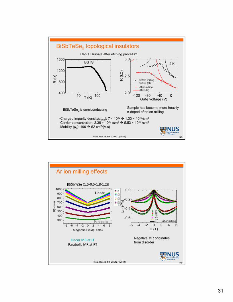
100 Before milling Before milling (Fit) After milling After milling (Fit)
L (n
m)
T (K)
L T -0.58 (before)
L T -0.56 (after)0 25 500
2
4
(x
10-7)
(-1T
-2)
T (K)
Phys. Rev. B, 90, 235427 (2014)
-A decay constant of -0.5 in L indicates two-dimensional (2D) electron-electron scattering for the sample before and after milling.-The behavior of surface states is unaffected by the introduction of disorder, as inferred from the similar values of α and the behavior of L.-Surface states are remarkably robust against external damage induced by ion milling.
Experimental setup
- Signal generator to excite magnetization dynamics in NiFe through a coplanar waveguide
- Voltmeter to measure spin pumping induced ISHE
- Vector network analyzer for FMR measurements
V
Magnetization oscillation provides high density spin currents into TI and a transverse voltage is detected in TI spin detector.
153Phys. Rev. B 90, 094403 (2014)
33
ISHE measurements
θsh = 0.01λsf = 6.2 nm
2 2 2 2 2
2 2 2 2
42tanh
28 4
r rf sfISHE BiSesh BiSe
BiSe sf
g h M MV dewd
R dM
157Phys. Rev. B 90, 094403 (2014)
0.0 0.2 0.4 0.6-2
0
2
4
6
8
10
3 GHz 4 GHz 5 GHz 6 GHz fitting
VIS
HE(
V)
B (kOe)
0 5 10 15 20 25 30 35 40
0.10
0.15
0.20
0.25
0.30
Data Fitting
VIS
HE/R
(V
/)
Bi2Se3 thickness (nm)
(c)
VISHE ~
R is resistance of the film
Js is induced spin current
θSH is spin Hall angle
SHsJR
Extracted spin Hall angle
• 1-2% of spin Hall angle is identified, which is already comparable to the best data from heavy metals (Pt, Ta).
• lso ~ λsf suggest that spin-orbit coupling is dominant source of spin scattering
-8 -4 0 4 8-0.06
-0.04
-0.02
0.00Data HLN fitting
G
(e
2 /h)
Magnetic field (T)0 50 100 150 200 250 300
0.8
1.2
1.6
2.0
2.4
Temperature (K)
sh (
%)
5
6
7
8
9
10
sf (
nm)
Spin orbit length, lso = 6.9 nm
161Phys. Rev. B 90, 094403 (2014)
34
No spin momentum locking
0 50 100 150 200 250 300
0.8
1.2
1.6
2.0
2.4
Surface (sh1)
Bulk (sh2)
sh
(%)
Temperature (K)
0 50 100 150 200 250 300
6
8
10
12
Temperature (K)
sf
(nm
)
(a) (b)
- Assumed spin Hall angle at opposite surfaces was taken to be of opposite signs.
- Spin Hall angle does not show any clear distinction between the surface and bulk value
- Momentum locking signature is not detected.
163Phys. Rev. B 90, 094403 (2014)
Comparison with other reports
Nature 511, 449 (2014) Nat. Mater. 13, 699 (2014)
Spin torque ferromagnetic resonance
measurements θSH = 2.0 – 3.5
Magnetization switching by current induced
spin orbit torque θSH = 140 – 425
In these experiments, a charge current flows through the TI material, unlike ours.
164
35
-1000 0 1000-4
-2
0
2
4
6 50 K 20 K
f = 8 GHz
300 K 200 K 100 K
V (V
)
H (Oe)
ST-FMR measurement of Bi2Se3/CoFeB
ST-FMR measurements with a lock-in amplifier at H = 35. ST-FMR signal (Vmix) can be fitted by a sum of symmetric and
antisymmetric Lorentzian functions:
mix s sym ext a asym ext( ) ( )V V F H V F H Vs: in-plane torque || on CFBVa: total out-of-plane torque
PRL 114, 257202 (2015) 167
In-plane spin-orbit torque ratio in Bi2Se3/CoFeB
0 50 100 150 200 250 3000.0
0.1
0.2
0.3
0.4 D 1 D 2 D 3
By Vs Only
D 1 D 2 D 3
T (K)
||
By Vs/V
a
|| (ǁ) increases steeply and nonlinearly to ~ 0.42 at low temperature and
could be almost 10 times larger than that at 300 K.
The polarization direction of || is consistent with spin-momentum-locked TSS.
|| by 1st and 2nd methods shows a significant difference below ~ 50 K, other
out-of-plane torque may contribution besides Oe.
170Wang et al., PRL 114, 257202 (2015)
1 10 100
200
300
400
T(K)
Rxx
(
)
Bi2Se
3 20 QL
36
0 50 100 150 200 250 300
0
1
2
3
T (K)
(Oe)
D 1 D 2 D 3
0 50 100 150 200 250 3000.0
0.1
0.2
0.3
0.4
T (K)
D 1 D 2 D 3
() also increases at low temperature similar to || (ǁ). Rashba-split state in 2DEG of Bi2Se3 is not the main mechanism for . Hexagonal warping in the TSS of Bi2Se3 can account for ().
Out-of-plane spin-orbit torque ratio in Bi2Se3/CoFeB
173Wang et al., PRL 114, 257202 (2015)
Out-of-plane torque in Bi2Se3
175
Wang et al., PRL 107, 207602 (2011)
Bi2Se3
Nomura et al., PRB 89, 045134 (2014)
-Recent reports showed there is substantial out-of-plane spin polarization due to
Hexagonal warping.
-Hexagonal warping in the TSS of Bi2Se3 can account for ().
37
Estimation of || from topological surface states (TSS)
0 50 100 150 200 250 300
0.6
0.9
1.2
0 50 100 150 200 250 3008
9
10
11
12
13
T (K)
n2
D (
10
13/c
m2 )
Bi2Se
3
I B
iSe/I C
FB
T (K)
By estimating ITSS:I2DEG:Ibulk, || from only TSS at low temperature is ~ 2.1 ±


![Strain and the optoelectronic properties of non-planar ... · D crystalline soft materials that acquire topological defects while conforming to non-planar shapes [12-15], the materials](https://static.documents.pub/doc/80x56/5b82c1247f8b9a934f8bb20e/strain-and-the-optoelectronic-properties-of-non-planar-d-crystalline-soft.jpg)


