29
| Date post: | 18-Dec-2015 |
| Category: |
Documents |
| Upload: | flora-hicks |
| View: | 222 times |
| Download: | 2 times |

Spintronics and Magnetic
SemiconductorsJoaquín Fernández-Rossier,
Department of Applied Physics, University of Alicante (SPAIN)
Alicante, June 18 2003
•Spintronics•Magnetic Semiconductors•Ferromagnetism in GaAsMn

Spintronics

Semiconductors
Source GateDrain
Semiconductor
Semiconductors:•Low carrier density (p, n)•Heterostructures•Electrical Control of p,n•Volatile information
Dimensional Reduction,
L<BMesoscopic Behavior,
L<ls
New exciting physics:Quantum
Hall Effects,Conductanc
e Quantizatio
n
Single electron transistor
Size reduction

Metallic Ferromagnets
Ferromagnetic metals:•Collective Coordinate •Permanent information•High carrier density•Heterostructures•Magnetic Control of current
‘Single atom’ magnet
New PhysicsGMR
L<lsr
Size reductio
n
Superparamagnetism
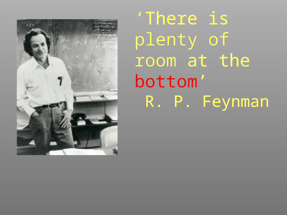
‘There is plenty of room at the bottom’
R. P. Feynman
‘There is plenty of room at the bottom’
R. P. Feynman

Alternative Approach: Spintronics
BUT:•Spin injection problem•Spin scattering problem
Source Gate Drain
InAs
Das and Datta spin transistor,APL 1990
•Rashba spin-orbit controls spin orientation•Spin dependent transmission controls resistance
High ResistanceLow Resistance
SPINTRONICS: Merger of semiconductor based
and ferromagnet based information technologies

Spintronics (from the table of contents of
“Semiconductor Spintronics and Quantum Computation”
• Device concepts• Interface Physics (spin injection)• Spin dynamics, spin decoherence• Optical Manipulation• Materials
Magnetic Semiconductors(materials for spintronics)

“History” of magnetic semiconductorsMaterial Year Tc Transport
EuO, EuS 1960-70 <65 K Insulating
(II,Mn)VI 1970-80 0 Semic.
PbSnMnTe
CdTeMn:N
ZnMnTe:X
1980-1990 <1.5 K P-type semiconduc.
InMnAs 1992 7 K Ins.
(Ga,Mn)As 1996 110 K Semic, bad metal
(Ga,Sb)Mn, GaP:Mn, GaN:Mn, ZnCrTe
1996-2003(DARPA time)
900 K??
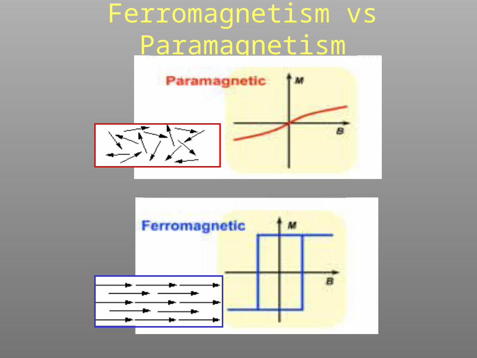
Ferromagnetism vs Paramagnetism

B C
Al Si
N O
P S
Ga Ge
In Sn
As Se
Sb
II
Zn
Cd
Hg
IV VIII VI
Te
EGEF
II-VIZn-SeZn-S Cd-Te
EGEF
Paramagnetic DMS
II
B C
Al Si
N O
P S
Ga Ge
In Sn
As Se
Sb
IV VIII VI
Te
Zn
Cd
Hg
Mn
(II,Mn)-VI(Zn,Mn)-Se(Zn,Mn)-S (Cd,Mn)-Te

B C
Al Si
N O
P S
Ga Ge
In Sn
As Se
Sb
II
Zn
Cd
Hg
IV VIII VI
Te
EGEF
III-VGa-AsIn-As Ga-Sb
EG
(diluted Ferromagnetic semiconductor)
B C
Al Si
N O
P S
Ga Ge
In Sn
As Se
Sb
Mn
II
Zn
Cd
Hg
IV VIII VI
Te
EF
(III,Mn)-V(Ga, Mn)-As(In, Mn)-As (Ga, Mn)-Sb
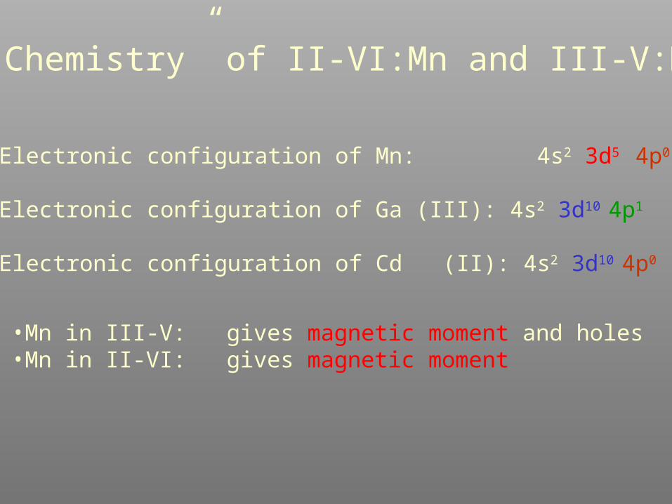
“Chemistry” of II-VI:Mn and III-V:Mn
Electronic configuration of Mn: 4s2 3d5 4p0
Electronic configuration of Ga (III): 4s2 3d10 4p1
Electronic configuration of Cd (II): 4s2 3d10 4p0
•Mn in III-V: gives magnetic moment and holes •Mn in II-VI: gives magnetic moment

Why DMS?
Y. OHNO et al., Nature 402, 790 (1999)
Magnetic Light emitting diode
•Spin injection•Compatible with GaAs
‘All semiconductor’ Magnetic Tunnel Junction•Large TMR (at 4 Kelvin)
Tanaka, Higo, PRL 2001
‘Electric Control of Ferromagnetism’
•First electrically tunable ferromagnet•Reversible change of Tc
H. Ohno, Nature (2000)
•Spin Injection•Heterostructures III-V + (III,Mn)-V•Magnetic control of transport•Electric control of Magnetism
BUT:• Working at low temperature•Small effects•Curie Temperature < 150 Kelvin
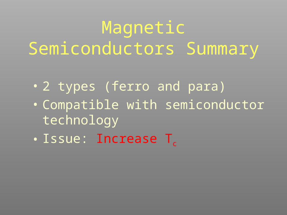
Magnetic Semiconductors Summary
• 2 types (ferro and para)• Compatible with semiconductor
technology
• Issue: Increase Tc
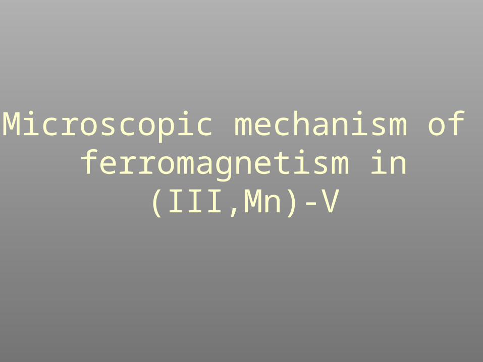
Microscopic mechanism of ferromagnetism in
(III,Mn)-V

The mechanism. Experimental evidence
• II-VI+Mn = PARAMAGNETIC• II-VI+Mn+electrons, PARAMAGNETIC• II-VI+Mn+ holes: FERROMAGNETIC• III-V+Mn= FERROMAGNETIC

Material: Ga(1-x) AsMnx
• Ferromagnetic below 160 kelvin• Homogeneous alloy for x<0.10
• Transport: p-doped semiconductor (p<cMn)
FERRO
PARA
x0.080.050.03
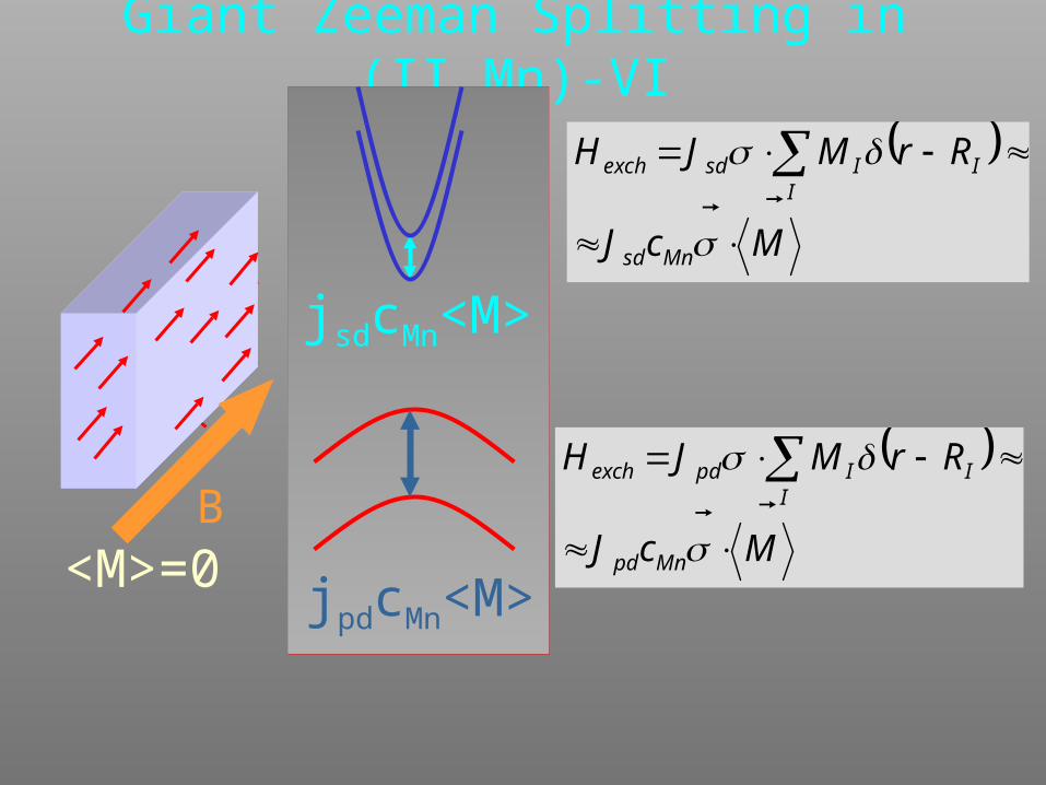
Giant Zeeman Splitting in (II,Mn)-VI
<M>=0
jsdcMn<M>
jpdcMn<M>
B
McJ
RrMJH
Mnsd
IIIsdexch
McJ
RrMJH
Mnpd
IIIpdexch
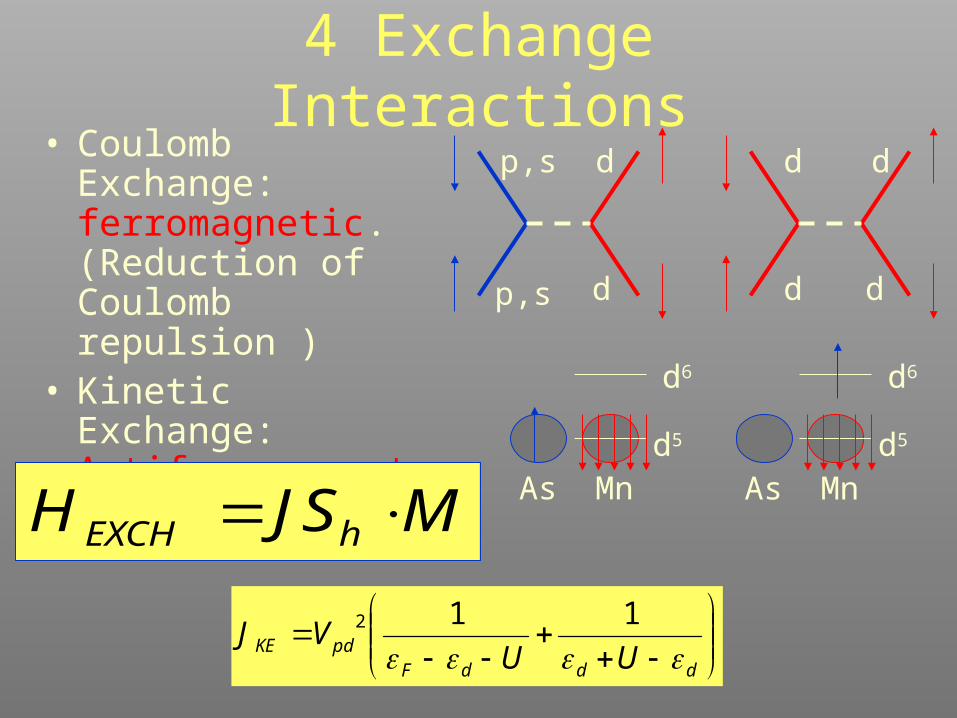
4 Exchange Interactions• Coulomb
Exchange: ferromagnetic. (Reduction of Coulomb repulsion )
• Kinetic Exchange: Antiferromagnetic
d5
d6
As Mnd5
d6
As MnMSJH hEXCH
p,s
p,s d
d
d
d d
d
dddF
pdKE UUVJ
112
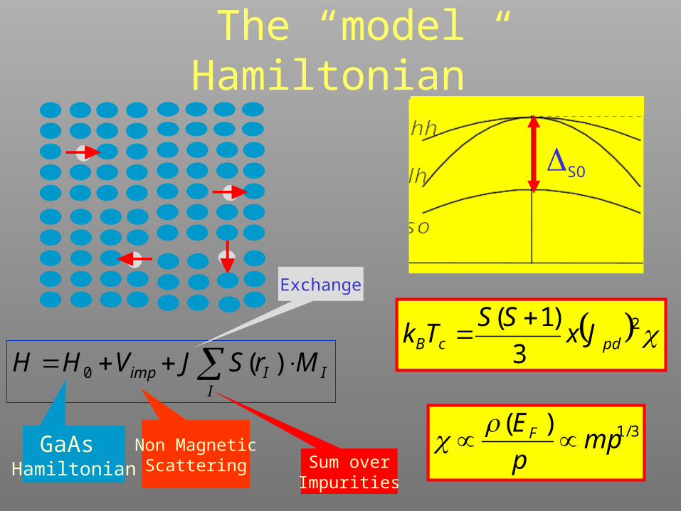
The “model Hamiltonian”
I
IIimp MrSJVHH
)(0
GaAs Hamiltonian
Non MagneticScattering
Exchange
Sum overImpurities
SO
2
3
)1(pdcB Jx
SSTk
3/1)(mp
p
EF

Carrier mediated ferromagnetism
MTSkMETMG Bcarrier
,
Entropic Penalty
Paramagneticgain
MSJMEMEcarrier
0
Functional of carrier density matrix
2
3
)1(pdcB Jx
SSTk
cB
pd Tk
SSJx
3
)1(2
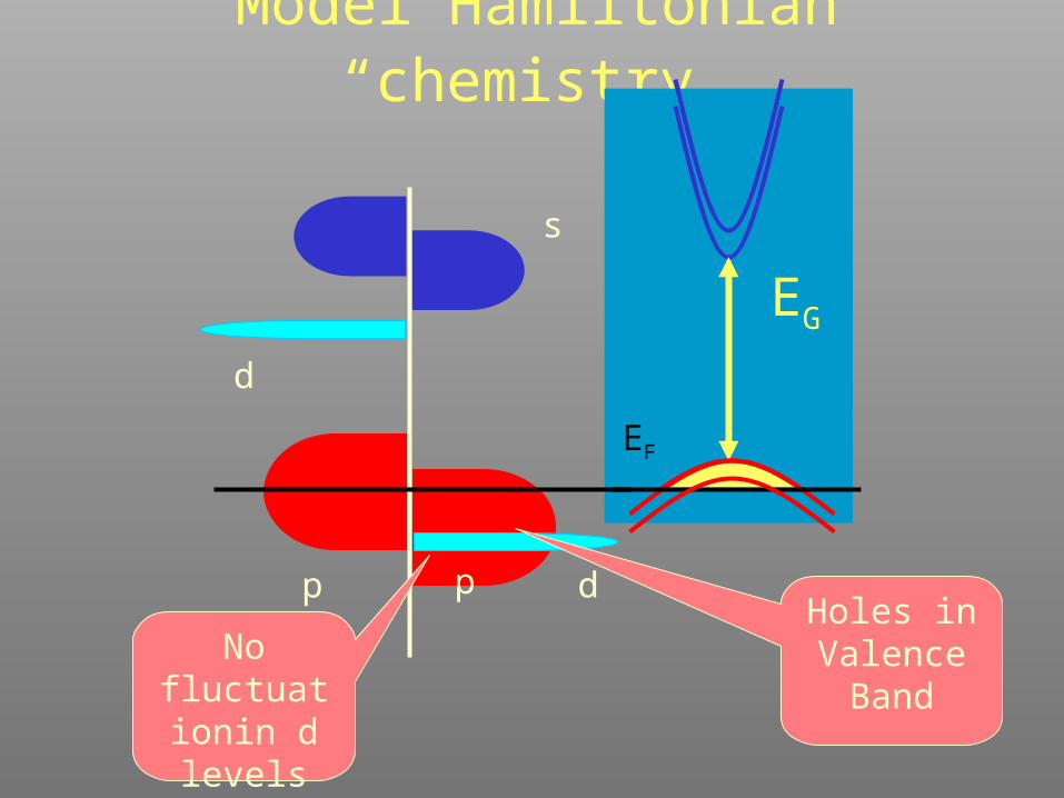
Model Hamiltonian “chemistry”
EG
EF
dp p
s
d
Holes in Valence
BandNo
fluctuationin d levels

dp p
s
dHoles in d
levels.
Hund Exchange
Half metal?
“Ab initio” “chemistry”
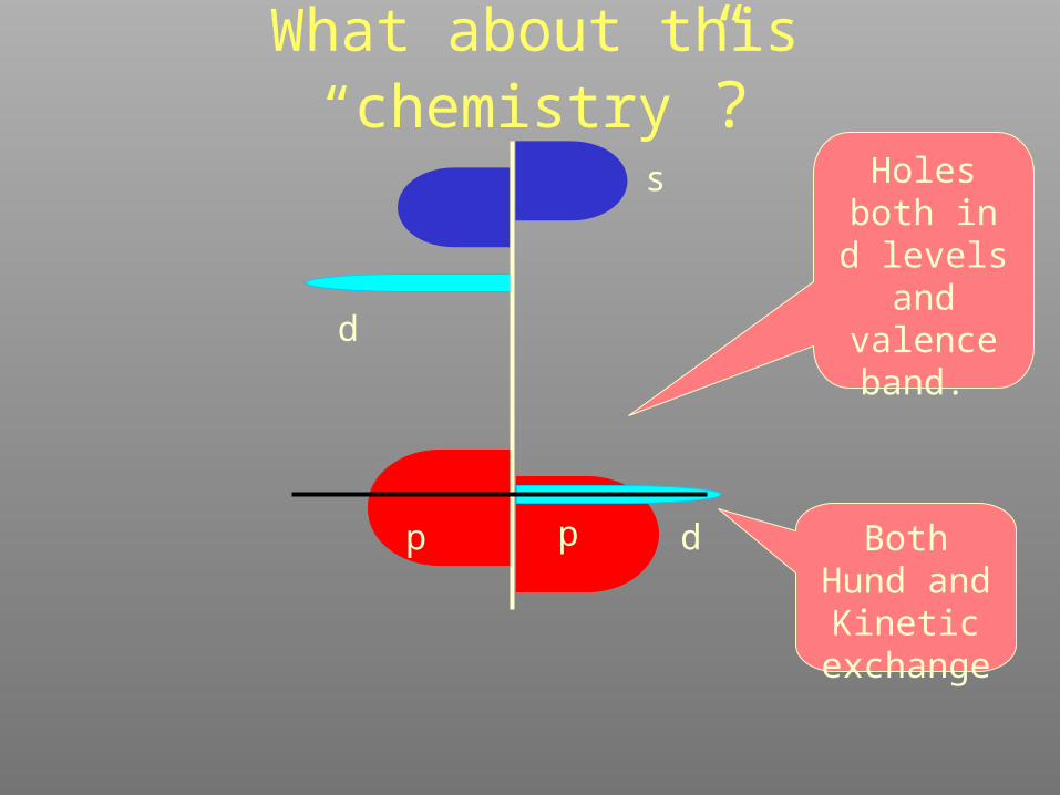
dp p
s
d
Holes both in d
levels and valence band.
Both Hund and
Kinetic exchange
What about this “chemistry”?

Microscopic Mechanism: Summary and questions
• Model Hamiltonian: no d-charge fluctuations, holes in valence band, kinetic exchange. Weak coupling
• “Double Exchange”: d charge fluctuations. Hund exchange. Strong coupling.
• Who is right? (from ab-initio)• Interpolation from DE to KE

C. PiermarocchiMichigan State
P.C. ChenUC Berkeley
L. J. ShamUCSD
JFR , in collaboration with
A. H. MacDonaldUT Austin
M. Abolfath,UT Austin
A. S. Núñez,UT Austin
Conclusions
• Spintronics: “make it happen” ideology
• Magnetic Semiconductors: bricks to build spintronics
• FM Mechanism: maybe an open problem.


