1 Spontaneous and strong multi-layer graphene n-doping on soda-lime glass and its application in graphene-semiconductor junctions D. M. N. M. Dissanayake 1* , A. Ashraf 1,2 , D. Dwyer 3 , K. Kisslinger 4 , L. Zhang 4 , Y. Pang 1,2 , H. Efstathiadis 3 and M. D. Eisaman 1,2,5* 1 Sustainable Energy Technologies Department, Brookhaven National Laboratory, Upton, NY 11973. 2 Department of Physics and Astronomy, Stony Brook University, Stony Brook, NY 11794. 3 Colleges of Nanoscale Science and Engineering (CNSE) at SUNY Polytechnic Institute, Albany, NY 12203. 4 Center for Functional Nanomaterials, Brookhaven National Laboratory, Upton, NY 11973. 5 Department of Electrical & Computer Engineering, Stony Brook University, Stony Brook, NY 11794. *Correspondence to: [email protected], [email protected]Scalable and low-cost doping of graphene could improve technologies in a wide range of fields such as microelectronics, optoelectronics, and energy storage. While achieving strong p-doping is relatively straightforward, non-electrostatic approaches to n-dope graphene, such as chemical doping, have yielded electron densities of 9.5x10 12 e/cm 2 or below. Furthermore, chemical doping is susceptible to degradation and can adversely affect intrinsic graphene’s properties. Here we demonstrate strong (1.33x10 13 e/cm 2 ), robust, and spontaneous graphene n-doping on a soda-lime-glass substrate via surface-transfer doping from Na without any external chemical, high-temperature, or vacuum processes. Remarkably, the n-doping reaches 2.11x10 13 e/cm 2 when graphene is transferred onto a p- type copper indium gallium diselenide (CIGS) semiconductor that itself has been deposited onto soda-lime-glass, via surface-transfer doping from Na atoms that diffuse to the CIGS surface. Using this effect, we demonstrate an n-graphene/p-semiconductor Schottky junction with ideality factor of 1.21 and strong photo-response. The ability to achieve BNL-111834-2016-JA
Transcript
1
Spontaneous and strong multi-layer graphene n-doping on soda-lime glass and its application in graphene-semiconductor junctions
D. M. N. M. Dissanayake1*, A. Ashraf 1,2, D. Dwyer3, K. Kisslinger4, L. Zhang4, Y. Pang1,2, H. Efstathiadis3 and M. D. Eisaman1,2,5*
1Sustainable Energy Technologies Department, Brookhaven National Laboratory, Upton, NY 11973. 2Department of Physics and Astronomy, Stony Brook University, Stony Brook, NY 11794. 3Colleges of Nanoscale Science and Engineering (CNSE) at SUNY Polytechnic Institute, Albany, NY 12203. 4Center for Functional Nanomaterials, Brookhaven National Laboratory, Upton, NY 11973. 5Department of Electrical & Computer Engineering, Stony Brook University, Stony Brook, NY 11794.
ln(Jo⁄T2) vs. 1/T (inset to Fig. 3a) yields Φb = 0.11eV, with a constant Richardson coefficient of
1.18x10⁻⁶ mAcm-2K-2. As is discussed below, this range for Φb (0.11eV – 0.29 eV) is lower than
expected, which we believe is due to surface defects and surface sodium doping of CIGS that
lowers the surface ionization potential of CIGS relative to the bulk.
7
The barrier height (Φb) is equal to the ionization potential of the CIGS semiconductor
(IPCIGS) minus the work function of graphene (ΦG), and represents the barrier that a hole in the
valence band of CIGS must overcome to reach the graphene interface and recombine with an
electron there. The activation energy (Ea), on the other hand, represents the characteristic energy
that governs the rate of minority carrier (electron) excitation into the conduction band of the p-
type semiconductor CIGS. In an intrinsic semiconductor, Ea is equal to half the bandgap, and for
a doped p-type semiconductor like CIGS, its value should be close to the bandgap energy, since
in this case the Fermi level is close to the valence band.
While fitting the J0 vs. T data to the Schottky barrier model allows us to determine Φb,
fitting this same data to the modified-Arrhenius/activation-energy model (Eqs. (S11), (S12), and
Fig. 3b) allows us to determine a value for Ea, which will indicate whether the recombination is
predominantly bulk or interfacial. The ideality factor n is expected to become temperature
dependent in the presence of tunneling. The measured I-V data is used to determine n as a
function of temperature and this is directly incorporated into Eq. (S11), which allows us to
separate the effects of Ea and n on the reverse saturation current density J0. Fig. 3b shows a modified Arrhenius-plot of n ln(Jo) vs. 1/T (where n is the ideality factor), yielding an activation energy (Ea) of 0.96 eV, which indicates dominant interfacial recombination since it is
less than the CIGS bandgap of 1.15eV (Ref. 26). We have demonstrated that this interfacial recombination can be reduced using a very thin (4nm) TiO2 blocking layer between graphene and CIGS, thereby improving Voc from 0.23 V to 0.49 V (Fig. S14). The space-charge width (Wd) of the diode is measured to be 190nm using C-V measurements (Fig. 3c). The approximate band structure of the Schottky diode is given in Fig. 3d. The difference between the CIGS ionization- potential (IPCIGS = 5.65eV (Ref. 27)), and graphene work function 4.69 eV (Ref. 28) modified by
8
the image-potential correction (0.15eV), gives a theoretical ΦbT = 0.81eV. Due to defects29 and
Na surface density30, IPCIGS is ~0.5eV lower, yielding ΦbT = 0.31eV, which is much closer to the
measured range of Φb = 0.11eV – 0.29eV. It is worth noting that even though the best-fit range
of Φb (0.11 eV – 0.29 eV) is much less than the best-fit value of Ea (0.96 eV), both models yield
good fits to the same J0 vs. T data due to the inclusion of the temperature-dependent n in the
activation-energy model.
In conclusion, we have demonstrated strong (1.33x10¹³ e/cm-2, corresponding to a Fermi
energy shift of +426meV.), robust, and spontaneous n-doping of graphene on the surface of a
low-cost industrial-grade soda-lime-glass substrate via surface-transfer doping from the Na. By
leveraging the Na diffusion through a p-type CIGS semiconductor deposited onto the soda-lime
glass, we applied this method to the formation of a graphene(n)/semiconductor(p) Schottky diode
with even stronger graphene n-doping (2.11x10¹³ e/cm-2, corresponding to a Fermi energy shift
of +536meV) than was achieved on bare glass. This method of n-doping does not require any
high-temperature annealing steps, and should be compatible with a wide range of
semiconductor/substrate systems. The junction properties, such as Schottky barrier height and
interfacial recombination rate, can be controlled by tuning the doping strength via the thickness
of a few-nm dielectric layer such as TiO2 or Al2O3. Advantages of this technique include the lack
of external chemicals whose doping strength decays over time, the ability to achieve strong and
persistent n-doping of graphene that is placed on top of a p-doped semiconductor, the ability to
n-dope graphene on a wide range of p-doped semiconductors via the use of a Na host that is in
direct contact with the graphene layer, and the ability to control the strength of the doping via the
use of a spacer layer (e.g., TiO2) between the Na host and the graphene layer. Disadvantages
include the possible restriction to p-doped semiconductors that are not too strongly affected by
9
the Na diffusion from the Na host to the graphene layer, in the case where the semiconductor lies
between the Na host and the graphene layer.
Strong, robust, and tunable graphene doping opens the door for the practical realization
of many envisioned applications of graphene such as touch screens and organic light-emitting
diodes1, where the reduction of sheet resistance is crucial to future success, and a broad array of
other applications where strong and tunable n-doping is important, such as microelectronics,
photodetectors, photovoltaics, electrochemical energy storage, and sensors2.
10
Methods CIGS deposition on Mo/SLG: Given in Supplementary Information, Section 2.
Device Fabrication: Supplementary Fig. S3 shows a schematic of the graphene/CIGS device
fabrication process. In order to make our GR/CIGS devices, 450 nm of SiO2 is first deposited on
top of the CIGS/Mo/SLG (BSG) substrates via plasma-enhanced chemical vapor deposition
(PECVD) at 160 oC at 1.6 nm/s rate. Next, 1x1 μm2 - 500x500 μm2 regions were patterned on the
PECVD SiO2 either using optical lithography (or ebeam lithography) techniques depending on
the feature size. E-beam was performed using the E-beam lithography JEOL JBX-6300FS
system on E-beam resist positive resist ZEP520A (spun at 2000 rpm for 40 sec annealed at 180
oC for 3 minutes) by exposing with a dose of 400 μC/cm2 at 100 keV and developed with
hexylacetate for 90 sec. In optical lithography, the tool MA6 Mask aligner was used with
positive optical resist S1811spun at 4000 rpm for 45 sec annealed at 110 oC for 1 minute, and
developed with MIF 312 3:2 with DI water for 1 minute. These patterned regions were then
etched via Reactive Ion Etching (RIE) (Oxford Plasmalab 100 ICP etcher) using a mixture of
(CHF3 and Ar) at 15 nm/min, until the CIGS was exposed. Commercially obtained CVD
graphene on Cu foil (Graphene Platform) was then transferred from the Cu substrates to the
SiO2/CIGS/Mo glass substrates. The graphene transfer was done by coating the graphene side of
the graphene/Cu foils with PMMA (10% w/w in chlorobenzene spun at 3000 rpm for 1min sec
and annealed at 140 oC per 1 min), oxygen plasma etching (March Plasma Etcher, 20 W, 100 mT
for 20 sec) the opposite side, and etching the Cu using ammonium persulfate (0.1 M) solution
overnight. As the Cu is etched away, the graphene/PMMA film floats on the etchant and it is
washed in de-ionized water (> 18 MΩ resistivity using a Millipore DI system) and it then
transferred, graphene-side down, onto the pattered CIGS/Mo/SLG or other control substrates
11
such as neat SLG or BSG substrate. Afterwards, graphene transferred substrates are annealed at
100 oC for 30 minutes in a vacuum oven to remove water, and are subsequently annealed at 200
oC for 15 minutes to soften the PMMA and promote conformal adhesion onto substrates. It is
found that the 200 oC annealing step is extremely critical in getting highly uniform, wrinkle- and
damage-free graphene films on the rough surfaces of CIGS and SiO2 substrates. Afterwards, the
PMMA is removed from the graphene by immersing in acetone overnight and the substrate is
further annealed in a Rapid Thermal Annealer at 375 oC in Ar( 96%): H2(4%) forming gas for 15
minutes for complete PMMA removal. Next, the graphene is etched following optical (ebeam)
lithographic patterning using oxygen plasma etch. (March plasma, 100 W and 100 mT for 1
minutes or Oxford Plasma Lab DRIE at 20 oC for 20 seconds in O2) using a negative tone resist
mask (E-beam lithography uses ma-N 2403, spun at 2000 rpm for 30 sec exposed at 200 μC/cm2
dose for 100 keV for electron beam and developed using ma-D 532 negative tone developer for 1
minute, Optical lithography uses maN-1410 negative resist spun at 3000 rpm for 30 seconds
exposed and developed in ma-D 533 for 1 minute). After etching the graphene, source-drain
electrical contacts (Au (30 nm)/Cr (5 nm)) are deposited using ebeam evaporation after optical
(ebeam) lithography patterning. Next, a 200nm top gate-dielectric layer (Al2O3) is blanket
deposited on GR/CIGS/Mo/SLG(BSG) or GR/SLG(BSG) substrates via Atomic Layer
Deposition at 1 Ǻ/cycle using (Tri Methyl Aluminum) TMA/Water precursor at 250 oC. On top
of the Al2O3, a semi-transparent top-gate (10nm of Au) is deposited via ebeam evaporation
following optical (ebeam) lithography patterning. Next, the source and drain electrodes are
exposed through the dielectric layer by RIE etching of Al2O3 using BCl3 by Oxford Plasmalab
100 ICP etcher, on a mask pattern using optical (ebeam) lithography.
Characterization: Given in Supplementary Information, Section 3.
12
References: 1. Novoselov, K. S. et al. A roadmap for graphene. Nature 490, 192-200 (2012). 2. Bonaccorso, F. et al. Graphene, related two-dimensional crystals, and hybrid systems for
energy conversion and storage. Science 347, 6217 (2015).
3. Tongay, S. et al. Rectification at Graphene-Semiconductor Interfaces: Zero-Gap Semiconductor-Based Diodes. Phys. Rev. X, 011002 (2012).
4. Yang, H. et al. Graphene Barristor, a Triode Device with a Gate-Controlled Schottky Barrier. Science 336, 1140 (2012)
5. Sinha, D. & Lee, J. U. Ideal Graphene/Silicon Schottky Junction Diodes. Nano Lett. 14, 4660 -4664 (2014).
6. Li, X. et al. Graphene-On-Silicon Schottky Junction Solar Cells. Adv. Mater. 22, 2743 – 2748 (2010).
7. Miao, X. et al. High Efficiency Graphene Solar Cells by Chemical Doping. Nano lett.12, 2745 - 2750 (2012).
8. Zhou, S. Y. et al. Substrate-induced bandgap opening in epitaxial graphene. Nature Mater. 6,770–775 (2007).
9. Schedin, F. et al. Detection of individual gas molecules adsorbed on graphene. N. Mater. 6, 652-655 (2007).
10. Wang, H., Maiyalagan, T. & Wang, X. Review on Recent Progress in Nitrogen-Doped Graphene: Synthesis, Characterization, and Its Potential Applications. ACS Catalysis 2, 781 - 784(2012).
11. Kim, Y., Yoo, J.M., Jeon, H.R. & Hong, B.H. Efficient n-doping of graphene films by APPE (aminophenyl propargyl ether): a substituent effect. Phys. Chem. Chem. Phys. 15, 18353-18356 (2013).
12. Dong, X. et al. Doping Single-Layer Graphene with Aromatic Molecules. Small 5, 1422 - 1426 (2009).
13. Caragiu, M. & Finberg, S. Alkali metal adsorption on graphite: a review. J. Cond. Mater. Phys. 17, R995–R1024 (2005).
14. Uchoa, B., Lin, C. Y. & Castro Neto, A. H. Tailoring graphene with metals on top. Phys. Rev. Lett. 77, 035420 (2008).
15. Sung, S. J. et al. Band gap engineering for graphene by using Na+ ions. Appl. Phys. Lett. 105, 081605 (2014).
16. Breitholtz, M., Kihlgren, T., Lindgren, S-Å. & Walldén, L. Condensation of Na metal on graphite studied by photoemission. Phys. Rev. B. 67, 235416 (2003).
17. Johnson, M., Stanberg, M. & Huges, H. Electronic-Structure of Alkali-metal Overlayers On Graphite Surface Science. Surface Science 178, 290-299 (1999).
18. Granath, K., Bodegard, M. & Stolt, L. The effect of NaF on Cu(In, Ga)Se2 thin film solar cells. Sol. Eng. Mater. Sol. Cells. 60, 279 - 293 (2000).
13
19. Wei, S., Zhang, S. & Zunger, A. Effects of Na on the electrical and structural properties ofCuInSe2. J. of Appl. Phys. 85, 7214 - 7218 (1999).
20. Kronik, L., Cahen, D. & Schock, H.W. Effects of sodium on polycrystalline Cu(In,Ga)Se2and its solar cell performance. Adv. Mater. 10, 31 - 36 (1998).
21. Niles, D. et al. Na impurity chemistry in photovoltaic CIGS thin films: Investigation with x-ray photoelectron spectroscopy. J. Vac. Sci. Technol. A. 15, 3044 - 3049 (1997).
22. Spanu, L., Sorella, S. & Galli, G. Nature and Strength of Interlayer Binding in Graphite.Phys. Rev. Lett. 103, 196401 (2009).
23. Witte, W., , R. & Raman, M. P. Investigations of Cu(In,Ga)Se2 thin films with various coppercontents. Thin Solid Films 517, 867 - 869 (2008).
24. Ferrari,A. C. et al. Raman Spectrum of Graphene and Graphene Layers. Phys. Rev. Lett. 97,187401 (2006).
25. Kohn, W. & Lau, K. H. Adatom Dipole Moments on Metals and Their Interactions. SolidState Commun. 18, 553 - 555 (1976).
26. Nadenau, V., Rau, U., Jasenek, A. & Schock, H.W. Electronic properties of CuGaSe2-basedheterojunction solar cells. Part I. Transport analysis. J. Appl. Phys. 87, 584 - 593 (2000).
27. Siebentritt, S. & Rau, U. Wide-Gap Chalcopyrites (Springer Series in Materials Science). 86,(2006)
28. Yu, Y. et al. Tuning the Graphene Work Function by Electric Field Effect. Nano Lett. 9, 3430-3434 (2009).
29. Hinuma, Y., Oba, F., Kumagai, Y. & Tanaka, I. Ionization potentials of (112) and (112) facetsurfaces of SuInSe2 and CuGaSe2. Phys. Rev. B. 86, 245433 (2012).
30. Heske, C., Fink, R., Umbach, E., Riedl, W. & Karg, F. Na induced effects on the electronicstructure and composition of Cu(In,Ga)Se2 thin film surfaces. Appl. Phys. Lett. 68, 3431 -3433 (1996).
Figure Legends
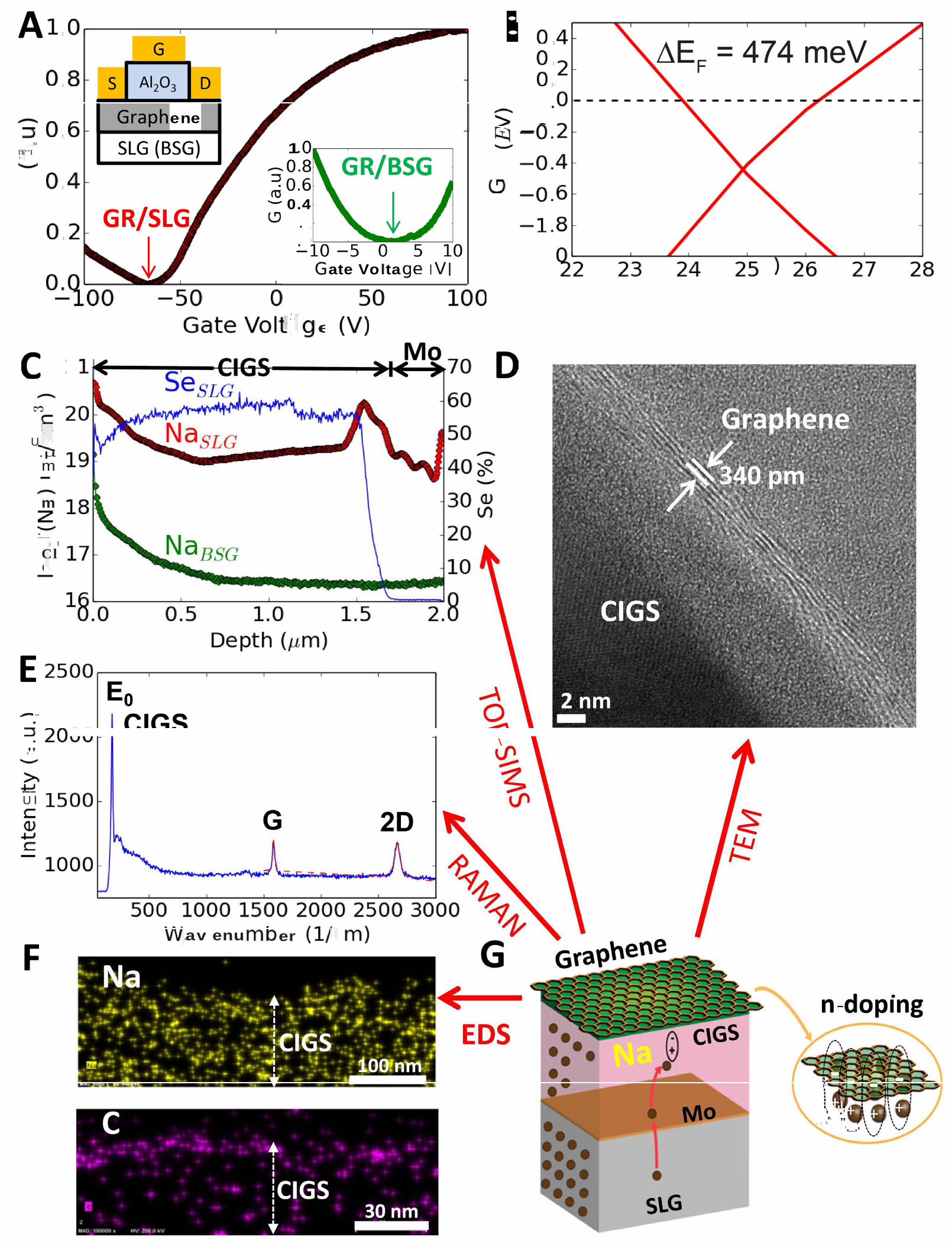
Figure 1. Surface-transfer n-doping of graphene from Na. (a) Conductance (G) (normalized)
vs. gate-voltage (VG) of graphene (GR)/soda-lime glass (SLG) and GR/borosilicate-glass (BSG)
(inset) measured in FET configuration (schematic). (b) DFT calculated dispersion curve showing
n-doping in graphene interacting with Na. (c) Na and Se depth-profiles in CIGS/Mo/SLG and
CIGS/Mo/BSG from TOF-SIMS. (d) Cross-sectional HR-TEM of GR/CIGS/Mo/SLG. (e)
Raman spectrograph of GR/CIGS/Mo/SLG showing E0 peak of CuIn0.7Ga0.3Se2 (177 cm-1), and
G peak (1585 cm-1) and 2D peak (2665 cm-1) of graphene. (f) EDS maps of GR/CIGS/Mo/SLG
14
showing Na (yellow, top) and C (purple, bottom). (g) Schematic of graphene n-doping
Figure S1. Comparison of n-doping density. Past chemical-doping strengths (red dots) compared to the strength of n-doping achieved in this work (blue dots) via Na surface- transfer doping from soda-lime glass (SLG) and CIGS-on-SLG. APPE = Aminophenyl propargyl ether.
2) CIGS deposition on Mo/SLGThe CIGS films used in these devices were deposited using three-stage thermal co- evaporation from elemental sources of Cu, In, Ga, and Se onto a heated Mo-coated soda- lime glass substrate (SLG). The SLG used was purchased from Guardian (product name: Ecoguard Mo-1, 3.0mm thickness) consisting of nominally ~15% Na2O (Ref. S1). The glass was coated with a Mo film by the glass manufacturer to a thickness of ~330nm (resistivity 15-22 µΩ-cm). The combined CIGS/Mo film thickness is typically measured to be 2.0μm, with Cu ratio (Cu/(In+Ga)) of 0.94, and Ga ratio (Ga/(Ga+In)) of 0.30 as measured by X-ray Fluorescence (XRF) (e.g. Sample # I1291 shown in Figure S1). XRF is used to measure copper and gallium ratios using a Ceres Technologies System SMX (Model #C06-01915-4002). The system was calibrated for CIGS films using the Standard–adjusted FP (fundamental parameters) method2,3 CIGS films of different compositions and thicknesses were measured using XRF. The film thickness was then measured using a stylus profilometer, and the film composition was measured using an inductively-coupled plasma (ICP) spectrophotometer with CIGS standard solutions. The
4
XRF system was calibrated using these values. When these same CIGS layers are
5
incorporated into standard (Mo/CIGS/CdS/iZnO/AZO) devices, the current-voltage curves yield power conversion efficiencies in the range of 15-18%.
Figure S2. AFM and TOF-SIMS on CIGS/Mo/SLG substrate.
6
2) Device fabrication
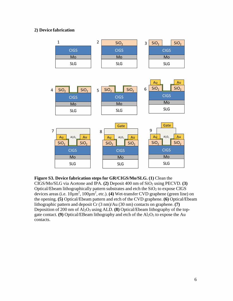
Figure S3. Device fabrication steps for GR/CIGS/Mo/SLG. (1) Clean the CIGS/Mo/SLG via Acetone and IPA. (2) Deposit 400 nm of SiO2 using PECVD. (3) Optical/Ebeam lithographically pattern substrates and etch the SiO2 to expose CIGS devices areas (i.e. 10µm2, 100µm2, etc.). (4) Wet-transfer CVD graphene (green line) on the opening. (5) Optical/Ebeam pattern and etch of the CVD graphene. (6) Optical/Ebeam lithographic pattern and deposit Cr (3 nm)/Au (30 nm) contacts on graphene. (7) Deposition of 200 nm of Al2O3 using ALD. (8) Optical/Ebeam lithography of the top- gate contact. (9) Optical/EBeam lithography and etch of the Al2O3 to expose the Au contacts.
7
3) Characterization methods TEM TEM thin-film samples were made via FIB using a FEI Helios Nanolab 600 Dualbeam (FIB/SEM) system employing a standard in-situ lift-out technique. Initial bulk milling was performed at 30 keV using a liquid metal gallium source. The specimen was subsequently cut free and transferred to a copper grid with a sharpened tungsten Omniprobe needle. Once attached to the TEM grid, the sample was thinned with progressively lower beam voltages down at to an approximate thickness of 50 nm with final milling performed at 2 keV. TEM images were acquired on a JEOL JEM2100F HRTEM operating at an accelerating voltage of 200 keV utilizing a 2K x 2K CCD camera.
EDS The energy-dispersive X-ray spectroscopy (EDS) chemical maps were acquired on a Hitachi2700C-STEM operated at 200kV.
SIMS A Physical Electrons 6650 Quadrupole SIMS was used to calculate the concentration of Na with respect to depth in the CIGS and glass samples. A CIGS and Obsidian implanted standard was used to determine the sputter rate and concentration of Na in the samples. The samples were first loaded into the sample exchange chamber and pumped down to 10-8 torr before being inserted to the main chamber. Cesium bombardment with a 60 degree angle of incidence, an accelerating voltage of 5 keV, and a beam current of 450 nA was used at 10-9 Torr in order to create the ions. The area scanned by the cesium beam had a raster size of 500x500µm and a 10% gate detection area. Charging at the surface was reduced using an electron beam. An electron multiplier detector was used to detect the positive secondary ions.
I-V Low temperature current-voltage (I-V) measurements were performed using the MMR technologies variable temperature micro-probe system. The temperature is varied from 83-300K in steps of 10K using a micro miniature refrigerator that cools the sample using the Joule-Thompson expansion of high-pressured nitrogen gas (chamber pressure <1mTorr). At each temperature an IV curve is extracted using a Kiethley 2600 source meter.
RAMAN Raman measurements were made using a WiTec Probe confocal Microscope at 514nm at 100x magnification. The optical power was kept at threshold in order not to locally heat the sample.
8
4) XPS measurements on SLG SIMScalibration
Figure S4. XPS analysis of the top 10 nm of soda-lime glass and calibration sample Obsidian.
Soda-lime glass (after removing ~25nm top layer by Ar+ sputtering) • Used Obsidian reference to obtain sensitivity factors for all elements except Ca
and Mg (XPS was not sensitive enough to detect Ca and Mg).• Using SiO2 density the following where measurements were obtained• 8% wt. of Na2O (≤2.5%)• 1.15x10²¹ Na atoms/cm3 (~5% atomic Na) for SLG
9
TOF-SIMS measurements
Figure S5. Na depth-profiles in SLG (red) and BSG (green) from (TOF)-SIMS. Data is calibrated using XPS analysis (Fig. 4) giving 1.15x10²¹ and 2.30x10²⁰ Na atoms/cm3 in the SLG and BSG respectively.
Figure S6. TOF-SIMS measurement on the CIGS/Mo/SLG (Ecoguard Mo-1, 3.0mm thickness and model and Na2O 8%) (Red) and CIGS/Mo/Borosilicate glass (Green) (Corning 1737, with <1% Na2O). Na peak at the CIGS-Mo edge at (1.5μm, 2.5μm) in (red, green) curve is from trace Na impurities in the Mo sputter target localized near the Mo-CIGS interface.
10
Figure S7. SIMS measurement on the top 20 nm of CIGS/Mo/SLG (Red, 8% Na2O) (red-curve) and CIGS/Mo/Borosilicate glass (Corning 1737, with <1% Na2O ) (green- curve). SLG surface Na density at 1nm is 4.18x1013cm-2, BSG surface Na density at 1nm is 6.16x1011 cm-2.z
11
5) Transconductance measurements
Figure S8. GR/CIGS/Mo/SLG (blue) and GR/TiO2/CIGS/Mo/SLG (green) transconductance measurements at 10 mV source-drain bias at room-temperature in the dark. Dirac point of GR/CIGS/Mo/SLG is -106V and GR/TiO2/CIGS/Mo/SLG is -92 V by a polynomial fit to the data. TiO2 thickness is 4 nm.
The shift in the Fermi Energy (ΔEF) can be written using Eq. (S1) where vF is the Fermi velocity (vF ::: 06m/s for graphene), N is the charge density of graphene, and ħ is Planck’s constant4.
∆EF = ħvF√rrN (S1)
In Eq. (S1) the charge density N is calculated considering the capacitance of the top dielectric (CTOP) and the applied potential (V) considering a parallel-plate capacitor with (N = ϵoϵAV⁄d) where ϵo, ϵ, A, d and V are vacuum permittivity (ϵo = 8.854x10⁻¹² F/m), relative dielectric constant (ϵ = 9.1), cross-sectional area (A = 104 μm2), and thickness of the dielectric (d = 252nm from TEM measurements).
At the asymptotic top-gate potential at the charge neutrality point (-106 V), N and ∆EF are calculated as 2.11x10¹³ e/cm-2 and 536meV, respectively for the GR/CIGS/Mo/SLG substrate. From this calculation, the graphene Fermi level at the charge neutrality point of -106 V is shifted up by ΔEF = +536meV, with respect to un- doped graphene.
12
6) Helmholtz equation to calculate thegraphene work-function shift on GR/CIGS/SLG (BSG)
Figure S9. Change of the potential on graphene due to the dipole moment from Na+ and image-charge.
The change of the potential on graphene due to the dipole moment from Na+ and image- charge is given by:
∆Φ = 2rreNaµ(8),EEO
where Llct is the change in the Graphene work function, µ is the dipole-moment of the Na+ and the image force on graphene, E is the relative dielectric constant, Eois the vacuum permittivity, e is electron charge, Na is the density of the ions per unit area on CIGS, and e is the fractional coverage of the ions on graphene.
µ(e) = 2dqNa ,
where d is the distance between graphene and the Na ion, and q is the charge of an electron. Taking d = 0.1 nm (i.e. the Na+ radius is 98 pm and elemental Na radius 186 pm), q = 1.6 X 10⁻¹⁹ C, Na = 4.18x1013 cm2 (CIGS/SLG) and 6.16x1011cm2 (CIGS/BS), E = 13.6 and Eo = 8.854 ∗ 10-12 F/m, and e is taken as 1.0 (complete coverage). e varies from 0.25-1.0 in previous studies5. The change in the graphene work function is calculated to be:
o Llct for CIGS/SLG = 0.69 eVo Llct for CIGS/BSG = 0.01 eV.
Figure S10. Linear photovoltaic current-voltage (I-V) behavior of the GR/CIGS/Mo/SLG (top). Blue curve is before Al2O3 and green curve is after Al2O3 under 11.14 mW/cm2
illumination. After Al203, J0 = 3.59x10⁻¹⁰ (A/cm2) and ideality-factor A=1.29. Before Al203: J0= 1.23x10⁻⁶ (A/cm-2) and A=91.53 fitting to the low-bias region (bottom).
14
Figure S11. Dark I-V of GR/CIGS/Mo/SLG device with an ideality factor of A=1.21.
15
8) VG dependent I-V measurement in GR/CIGS/Mo/SLG
Figure S12. I-V behavior in the dark with different top-gate potentials shown in Table T1.
VG (V) J0 (A/cm2) n Data point color 50 8.2 x 10⁻¹⁰, 1.22 black 0 8.56x10⁻¹⁰, 1.21 blue
-50 1.02 x10⁻⁹, 1.22 red -100 1.17 x10⁻⁹
1.23 purple
Table ST1. Fitting parameters at different VG. n is the ideality factor, VG is gate-voltage, and J0 is the reverse saturation current density.
16
o
N = O G F
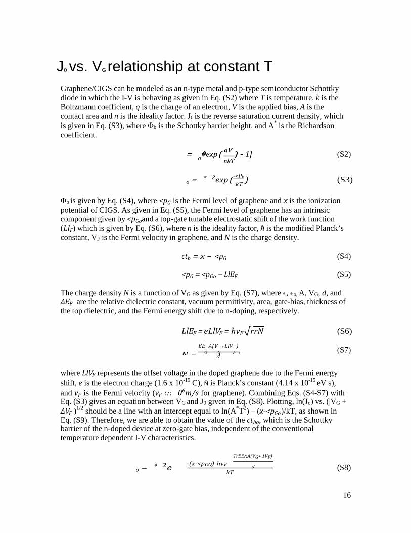
J0 vs. VG relationship at constant T Graphene/CIGS can be modeled as an n-type metal and p-type semiconductor Schottky diode in which the I-V is behaving as given in Eq. (S2) where T is temperature, k is the Boltzmann coefficient, q is the charge of an electron, V is the applied bias, A is the contact area and n is the ideality factor. J0 is the reverse saturation current density, which is given in Eq. (S3), where Φb is the Schottky barrier height, and A* is the Richardson coefficient.
= exp ( qV ) - 1] (S2) nkT
o = ∗ 2exp ( -<Pb
kT ) (S3)
Φb is given by Eq. (S4), where <pG is the Fermi level of graphene and x is the ionization potential of CIGS. As given in Eq. (S5), the Fermi level of graphene has an intrinsic component given by <pGoand a top-gate tunable electrostatic shift of the work function (LlF) which is given by Eq. (S6), where n is the ideality factor, ħ is the modified Planck’s constant, VF is the Fermi velocity in graphene, and N is the charge density.
ctb = x - <pG (S4)
<pG = <pGo - LlEF (S5)
The charge density N is a function of VG as given by Eq. (S7), where ϵ, ϵo, A, VG, d, and ΔEF are the relative dielectric constant, vacuum permittivity, area, gate-bias, thickness of the top dielectric, and the Fermi energy shift due to n-doping, respectively.
LlEF = eLlVF = ħvF√rrN (S6)
EE A(V +LlV ) , (S7) d
where LlVF represents the offset voltage in the doped graphene due to the Fermi energy shift, e is the electron charge (1.6 x 10⁻¹⁹ C), Ñ is Planck’s constant (4.14 x 10⁻¹⁵ eV s), and vF is the Fermi velocity (vF ::: 06m/s for graphene). Combining Eqs. (S4-S7) with Eq. (S3) gives an equation between VG and J0 given in Eq. (S8). Plotting, ln(Jo) vs. (|VG + ΔVF |)1/2 should be a line with an intercept equal to ln(A*T2) – (x-<pGo)/kT, as shown in Eq. (S9). Therefore, we are able to obtain the value of the ctbo, which is the Schottky barrier of the n-doped device at zero-gate bias, independent of the conventional temperature dependent I-V characteristics.
TrEEOA(VG+.1VF)
o = ∗ 2e -(x-<pGO)-ħvF d
kT (S8)
17
ln( o) = ln( ∗ 2) + - ctbo - ħvF rEEOA(VG+LlVF)d
jk (S9)
Figure S13. ln(J0) vs. (|VG + LlVF|)1/2.
Taking the Richardson constant (A*) as A*=1.18x10⁻⁶ mAcm-2K-2 (from the temperature dependent analysis in Fig. S15), the intercept in Fig. S13 at (VG + ΔVF )=0 is -13.56:
-13.56= -ctbo/k + ln(300 x 300 x 1.18 x 10-6) = -ctbo/k + ln(0.106)
ctbo/k = 13.56 – 2.24 = 11.31
ctbo= 11.31 x 26 meV = 0.29 eV
18
B
O OO
9) Recombination analysis onGR/CIGS/Mo/SLG
For an ideal Schottky barrier, o = ∗ 2exp ( -<Pb
kT ) where ctb is the Schottky barrier height. By fitting ln (IO ) vs. 1000/T, we obtain Schottky barrier height of φ = 0.11eV
T2 b
and A* = 1.18x10⁻⁶ mAcm-2K-2. This is assuming a fixed Richardson constant A*.
For finite density of states, A* becomes temperature dependent and the Landauer transport model is used as given in Eq. (S10) below6:
qDo 2 ctB -ctB⁄kB
o = (k )T
( + 1)] e kB
, (S10)
where DO = [2/(rr(Ñ vF)2] with Ñ Planck’s constant and vF the Fermi velocity (vF ::: 106m/s for graphene) represents the prefactor that gives the graphene density of states when multiplied by the energy, and T is the time scale for carrier injection from the contact. In order to fit this equation to the data shown in the main panel of Fig. 3a, wefind the best-fit values for two parameters: c ≡ qDO and ct . The blue solid best-fit line
T B shown in the main panel to Fig. 3a is Eq. (S10) with best-fit parameter values of c ≡ qDO
T
= 58.15 and ctB = 0.13 eV. We observe that the diode quality factor is temperature dependent which means that there is a strong contribution of tunneling in the recombination mechanism. High ideality factors at low temperatures suggest a transition from tunneling dominated interface recombination at low temperatures to standard Shockley-Read-Hall (SRH) behavior at room temperature.
The same J0 data can be used in a different model where the diode quality factor, n, is taken into account. In this model the reverse saturation current, J0 can be written as a function of temperature T, activation energy, Ea, the diode quality factor, n, and J00, which is a weakly temperature-dependent prefactor.
qV -Ea qV
= O exp (nkT) = OO exp (nkT) exp(nkT), (S11)
Compared to the typical definition of activation energy, where the exponential term containing Ea does not include the ideality factor n in the denominator, Eq. (S11) includes n in the denominator of both exponential terms to account for the temperature dependence of n. In the case of tunneling, where the ideality factor n becomes temperature dependent, we can rewrite Eq. (S11) to obtain
n ln( ) = (-Ea) + n ln( ) . (S12) kT
Assuming that J00 is temperature independent, we can extract the activation energy Eausing a modified Arrhenius plot (Ref. S16), n ln(J0) vs.1/T (in contrast to a standard
19
Arrhenius plot - ln(J0) vs.1/T – that one would use when the denominator of the exponential term in Eq. (S11) containing Ea does not include the ideality factor n). In an
20
intrinsic semiconductor, the activation energy is equal to half the bandgap, and for a p- doped semiconductor it should be close to the bandgap energy since the Fermi energy is close to the valence band. We extract an activation energy Ea = 0.96 eV which is lower than the CIGS bandgap of 1.15 eV, suggesting a contribution of tunneling enhanced interfacial recombination (Ref. S16). We note that in our case, and in previous studies17,18, when extracting Ea for Schottky barrier devices, the difference between Ea and ctB is largely determined by the value of n and its temperature dependence.
Hole blocking layer between n-graphene and CIGS
Figure S14. Graphene/CIGS/Mo/SLG (blue) and Graphene/TiO2/CIGS/Mo/SLG (red) I- V measurements in the dark (dashed) and 11.14 mW white-light (solid). The open circuit voltage without TiO2 is VOC = 0.23 V, and with a 4nm TiO2 hole blocking layer VOC = 0.49 V.
21
10) Density functional theory (DFT)calculations
DFT calculation of a free standing graphene monolayer
The graphene monolayer crystal structure is described by the primitive translation vectors:
√3 1a_ 1 = a 2 , 2
√3 1a2 = a 2 , 2
a3 = a(0,0,6)
where a = 2.46Å is the lattice constant. a3 is the lattice vector in the z direction, which adds a 6Å vacuum gap between graphene layers. Since we use periodic boundary condition in three directions, the vacuum guarantees that the graphene monolayer is isolated from adjacent layers. The atomic positions are:
1 (C) = (0,0)
1 _2 (C) = a , 0
√3
Figure S15.The honeycomb structure of the graphene monolayer. a1 and a2 are the two lattice vectors in x,y plane. The primitive unit cell is shown by the lattice vectors and the dotted line and 1 and 2 denote the two carbon atoms per unit cell.
22
Density functional theory calculation of free-standing graphene with Na The graphene-monolayer-with -sodium crystal structure is described by the primitive translation vector as shown in:
√3 1_a1 = a 2 , 2 , 0
√3 1a2 = a 2 , 2 , 0
a3 = a(0,0,12)
Figure S16. The honeycomb structure of the graphene monolayer with sodium (purple). a1 and a2 are the two lattice vectors in x,y plane. The primitive unit cell is shown by the lattice vectors and the dotted line and 1 and 2 denote the two carbon atoms per unit cell; the purple atom is the sodium atom in the primitive unit cell.
Since we introduce the sodium atom into the graphene monolayer crystal structure, we add a thicker vacuum layer (12Å) to isolate the graphene-monolayer-with-sodium system. The atomic positions are:
1 (C) = (0,0,0)
1 _2 (C) = a , 0,0
√3
1 _ 3 (Na) = a , 0,1
√3
All the calculations are performed by DFT, which is implemented in GPAW based on the projector-augmented wave (PAW) method and the atomic simulation environment (ASE) (Ref. S7-S9). We use the default Finite Difference mode, which means that the wave
23
function will be expanded on a real space grid, and the grid spacing is 0.18Å. The Perdew-Burke-Ernzerhof (PBE), which is a generalized gradient approximation (GGA)
24
type, is adopted. The Brillouin-zone is sampled using Γ-centered 5 × 5 × 1 Monkhorst- Pack k-points. The electrons will be distributed into the available energy levels according to the Fermi Dirac Distribution, and the width kB T = 0.05 eV. The convergence criterion is 1e-12 for the Poisson solver.
Figure S17. DFT calculation of the band-structure of the graphene monolayer. It clearly shows the linear behavior of the bands near the vicinity of K at the Fermi energy. The conduction and valence bands cross at the Dirac point indicating no intrinsic doping of the structure.
Figure S18. DFT calculation of the band- structure of graphene monolayer interacting with the Na (density: 1 Na atom per primitive unit cell). The result shows a 474meV shift in the Fermi level from the Dirac point at K, which indicates n-doping of graphene from Na.
25
11) C-V measurements
Figure S19. C-V measurement on GR/CIGS/Mo/SLG at 50 mVrms a.c. voltage at 0 V d.c. bias in the frequency range 100 Hz – 100 KHz in dark.
Considering the junction as an RC-equivalent circuit, the junction capacitance (Cp) is calculated as 53.32 nF/cm2 by plotting Im (1) vs. f (inset) using Eq. (S13). Considering
z uniform charge density in the space-charge region, the space-charge width (Wd) is calculated to be 190.94 nm.
Im (1) = 2rr C (S13) z
26
References [S1] Al-Thani, H. & Williamson, D. The Effect of Mo Back Contact on Na Out-Diffusion and Device Performance of Mo/Cu, NREL/CP-520-32254, (2002). [S2] Dwyer, D., Schujman, S., Novak, J., Metacarpa, D. and Haldar, P. Selenium flux effects on Cu(In,Ga)Se2 growth rate, and control by in-line X-ray fluorescence, Proc. of the 39rd IEEE Photovoltaic Specialists Conference 1957-1960 (2013). [S3] Gabor, A. et al. Band-gap engineering in Cu(In,Ga)Se2 thin films grown from (In,Ga)2Se3 precursors, Solar Energy Materials and Solar Cells. 41/42 247-260 (1996). [S4] Das, A. et al. Monitoring dopants by Raman scattering in an electrochemically top- gated graphene transistor. Nature. Nanotec. 3, (4) 210–215 (2008). [S5] Caragiu, M. & Finberg, S. Alkali metal adsorption on graphite: a review. J. of Physics-condensed matter. 17, R995–R1024 (2005). [S6] Sinha, D. & Lee, J. U. Ideal Graphene/Silicon Schottky Junction Diodes. Nano Lett. 14, 4660–4664 (2014). [S7] Mortensen, J., Hansen, L. & Wedel, K. Real-space grid implementation of the projector augmented wave method. Phys. Rev. B. 71, 035109, (2005). [S8] Enkovaara, J. et al. Electronic structure calculations with gpaw: a real- space implementation of the projector augmented-wave method. J. of Phys.: Condensed Matter. 22, 253202 (2010). [S9] Bahn, S. & Jacobsen, K. An object-oriented scripting inter- face to a legacy electronic structure code. Computing in Science & Engineering. 4, 56–66 (2002). [S10] Dong, X. et al. Doping Single-Layer Graphene with Aromatic Molecules. Small 5, 1422 - 1426 (2009). [S11] Wang, Z. et al. Air-stable n-type doping of graphene from overlying Si3N4 film. Appl. Surf. Sci. 307, 712-715 (2014). [S12] Kim, Y., Yoo, J.M., Jeon, H.R. & Hong, B.H. Efficient n-doping of graphene films by APPE (aminophenyl propargyl ether): a substituent effect. Phys. Chem. Chem. Phys. 15, 18353-18356 (2013). [S13] Park, J. et al. Work-Function Engineering of Graphene Electrodes by Self- Assembled Monolayers for High-Performance Organic Field-Effect Transistors. J. Phys. Chem. Lett. 2, 841–845 (2011). [S14] Zhang, C. et al. Synthesis of Nitrogen-Doped Graphene Using Embedded Carbon and Nitrogen Sources. Adv. Mater. 23, 1020-1024 (2011). [S15] Huh, S. et al. Selective n-Type Doping of Graphene by Photo-patterned Gold Nanoparticles. ACS Nano 5, 3639–3644 (2011). [S16] Nadenau, V., Rau, U., Jasenek, A. & Schock, H.W. Electronic properties of CuGaSe2-based heterojunction solar cells. Part I. Transport analysis. J. Appl. Phys. 87, 584 - 593 (2000). [S17] Asghar, M., Mahmood, K., Faisal, M., and Hasan, M. A. Electrical characterization of Au/ZnO/Si Schottky contact. J. Phys.: Conf. Ser. 439, 012030 (2013). [S18] Wu, C. S. et al. Novel GaAs/AlGaAs Multiquantum-Well Schottky-Junction Device and its Photovoltaic LWIR Detection. IEEE Transactions on Electron Devices 39, 234-241 (1992).


![Stable hole doping of graphene for low electrical ...tanner/PDFS/Tongay11Naontech-Graphene-dopin… · used in optoelectric devices/solar cells [6, 8]inanattemptto replace ITO, which](https://static.documents.pub/doc/80x56/5f3e6d7699cc716c29284b1b/stable-hole-doping-of-graphene-for-low-electrical-tannerpdfstongay11naontech-graphene-dopin.jpg)


