112
IMPACT Center For Advancement of MEMS/NEMS VLSI A DARPA N/MEMS Science and Technology Fundamentals Research Center 20 April 2007 Spring 2007 Industrial Affiliates Meeting
Page 1Industrial Affiliates Meeting, April 20, 2007
IMPACT Center For Advancement of MEMS/NEMS VLSI
A DARPA N/MEMS Science and Technology Fundamentals Research Center
20 April 2007
Spring 2007Industrial Affiliates Meeting

Page 2Industrial Affiliates Meeting, April 20, 2007
Agenda
8:30 – 9:00 am Registration – Coffee
9:00 – 9:15 Welcome and Introductions
9:15 – 9:30 IMPACT Center Overview
9:30 – 10:15 Thrust 1. Physics of Failure of Contacting MEMS Devices
10:15 – 10:45 Coffee Break
10:45 – 11:30 Thrust 2. Physics of Failure of Non-Contacting MEMS Actuators
11:30 – 12:00 Parallel Sessions: Industry Partner Caucus Scientific Advisory Board Caucus
12:00 – 12:30 pm Feedback to PIs
12:30 – 1:30 Lunch

Page 3Industrial Affiliates Meeting, April 20, 2007
Challenges
Grand Challenge: Realization of Reliable and Cost-Effective MEMS/NEMS-based Microsystems to Enable Revolutionary Military Capabilities
Grand Challenge: Realization of Reliable and Cost-Effective MEMS/NEMS-based Microsystems to Enable Revolutionary Military Capabilities
The proposed, fundamental physics-based, experimentally validated MEMS/NEMS multi-physics models will serve as foundation for sophisticated computer-aided design environments that will enable and expedite the design process for future, cost-effective, MEMS-based microsystems
• Enhance the understanding of experimentally-observed physical principles and processes governing MEMS/NEMS performance
• Develop deterministic & stochastic computer tools for predictive assessment of MEMS/NEMS device and system long-term performance
• Expedite the design process of MEMS-enabled micro-systems
• Enable the full exploitation of MEMS/NEMS technology for enhancing the functionality of integrated micro- and nano-systems
• Surface Physics: Complex interactions between material properties and structural behavior
• Reliability Physics: Multi-domain physics of failure attributed to
–dielectric charging–mechanical deformations –micro-cracking as a result of material defects in complex micro-structures
• Modeling: Innovative models and modeling methodologies to capture the multi-domain physics and stochastic, multi-scale complexity of MEMS/NEMS devices
ImpactFocus Center ObjectivesFundamental Science

Page 4Industrial Affiliates Meeting, April 20, 2007
Center Mission
Experimentaldemonstrations
Physics-basedmodel formulation
MEMS Microsystems Design Environment
Physics-Based Models
Interactive Design Visualization
Physics• Mechanical• Materials• Thermal• Electrical
MEM
S S&
T Fu
ndam
enta
lsFo
cus
Futu
re O
ppor
tuni
ties • Through experimental investigation
and fine-scale, physics-based, multi-domain modeling, understand the fundamental principles governing MEMS/NEMS performance
• Demonstrate a set of multi-domain, multi-scale computer models for predictive device functionality and life-time assessment
• Demonstrate design methodologies, and a mature design environment
• Utilize the design environment for the full exploitation of MEMS/NEMS devices in highly integrated micro-and nano-systems
Page 5Industrial Affiliates Meeting, April 20, 2007
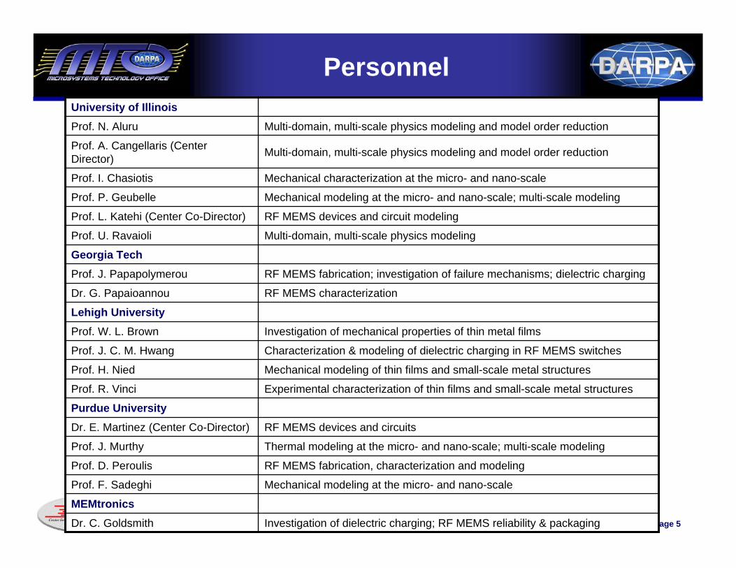
Personnel
RF MEMS characterizationDr. G. Papaioannou
Investigation of dielectric charging; RF MEMS reliability & packagingDr. C. Goldsmith
MEMtronicsMechanical modeling at the micro- and nano-scaleProf. F. Sadeghi
RF MEMS fabrication, characterization and modelingProf. D. Peroulis
Thermal modeling at the micro- and nano-scale; multi-scale modelingProf. J. Murthy
RF MEMS devices and circuitsDr. E. Martinez (Center Co-Director)
Purdue UniversityExperimental characterization of thin films and small-scale metal structuresProf. R. Vinci
Mechanical modeling of thin films and small-scale metal structuresProf. H. Nied
Characterization & modeling of dielectric charging in RF MEMS switchesProf. J. C. M. Hwang
Investigation of mechanical properties of thin metal filmsProf. W. L. Brown
Lehigh University
RF MEMS fabrication; investigation of failure mechanisms; dielectric charging Prof. J. Papapolymerou
Georgia TechMulti-domain, multi-scale physics modelingProf. U. Ravaioli
RF MEMS devices and circuit modelingProf. L. Katehi (Center Co-Director)
Mechanical modeling at the micro- and nano-scale; multi-scale modelingProf. P. Geubelle
Mechanical characterization at the micro- and nano-scaleProf. I. Chasiotis
Multi-domain, multi-scale physics modeling and model order reductionProf. A. Cangellaris (Center Director)
Multi-domain, multi-scale physics modeling and model order reductionProf. N. Aluru
University of Illinois

Page 6Industrial Affiliates Meeting, April 20, 2007
IMPACT Center Organization
NonNon--Contacting ActuatorsContacting ActuatorsCharacterization Characterization
and Model Validationand Model ValidationTask Lead: PapapolymerouTask Lead: Papapolymerou
Characterization Characterization Of Degradation Of Degradation
BehaviorBehaviorPurdue, Lehigh, UIUCPurdue, Lehigh, UIUC
Validation Validation TestbedsTestbedsGaTechGaTech, Purdue, Lehigh, Purdue, Lehigh
Reliable MEMS Switch DesignReliable MEMS Switch DesignThrust Lead: C. GoldsmithThrust Lead: C. Goldsmith
MultiMulti--Domain Domain Physics/MultiPhysics/Multi--ScaleScale
ModelingModelingTask Lead: AluruTask Lead: Aluru
ElectricalElectrical--Mechanical Mechanical
ModelingModelingUIUC, Purdue,UIUC, Purdue,
LehighLehigh
ThermalThermal--Mechanical Mechanical
ModelingModelingUIUC, PurdueUIUC, Purdue
Switch Characterization Switch Characterization and Model Validationand Model Validation
Task Lead: HwangTask Lead: Hwang
Dielectric Dielectric ChargingCharging
Lehigh, Lehigh, GaTechGaTech
Characterization Characterization Of Degradation Of Degradation
BehaviorBehaviorPurdue, Lehigh, UIUCPurdue, Lehigh, UIUC
Validation Validation TestbedsTestbedsGaTechGaTech, Purdue, Lehigh, Purdue, Lehigh
Reliable NonReliable Non--Contacting Contacting Actuators Device DesignActuators Device DesignThrust Lead: D. PeroulisThrust Lead: D. Peroulis
Dr. Dennis Polla, DARPA PMDr. Dennis Polla, DARPA PM
Andreas Cangellaris, DirectorAndreas Cangellaris, DirectorLinda Katehi, CoLinda Katehi, Co--DirectorDirector
Edgar Martinez, CoEdgar Martinez, Co--DirectorDirector
IndustrialIndustrialAdvisory BoardAdvisory Board
ScientificScientificAdvisory CommitteeAdvisory Committee

Page 7Industrial Affiliates Meeting, April 20, 2007
Industry Partners
Industrial Advisory Board– Representatives from the Center’s
industrial affiliates– Advisory body to Center’s
Leadership on issues related to:• Research activities
– Changes in research focus or directions
– Review on new tasks and funding recommendation
• Opportunities for collaboration with other research teams in academia, industry and national labs
• Issues on technology transfer – Leveraging IR&D activities for
knowledge development in the Center
• MEMtronics• BAE Systems• EMAG Technologies• Fluent• Innovative Design & Technology• nGimat• Raytheon• Rockwell Collins• Rogers Corporation• Cadence Design Systems• Mentor Graphics• NASA Goddard Space Flight Center• Sandia National Laboratories
• MEMtronics• BAE Systems• EMAG Technologies• Fluent• Innovative Design & Technology• nGimat• Raytheon• Rockwell Collins• Rogers Corporation• Cadence Design Systems• Mentor Graphics• NASA Goddard Space Flight Center• Sandia National Laboratories

Page 8Industrial Affiliates Meeting, April 20, 2007
Scientific Advisory Board
• John (Jack) Ebel Air Force Research Lab
• Anantha Krishnan Lawrence Livermore Lab
• Art Morris wiSpry, Inc.
• Chris Nordquist Sandia National Lab
• Dev Palmer Army Research Office
• Barry Perlman US Army RDECOM
• Daniel Powell NASA

Page 9Industrial Affiliates Meeting, April 20, 2007
Research PlanThrust 1: Reliable contacting MEMS switches
Task 1.1: Fundamentals of material and structural effects and validated models for contacting MEMSTask 1.2: Fundamentals of electrostatic effects and dielectric charging in contacting MEMS Task 1.3: Multi-physics/multi-scale models and design framework for contacting MEMS
Thrust 2: Fundamentals of reliable non-contacting, large-displacement MEMS actuators
Task 2.1: Fundamentals of material and structural effects and validated models for non-contacting MEMS/NEMS actuators Task 2.2: Fundamentals of thermal transport and models for non-contacting MEMS/NEMS actuatorsTask 2.3: Multi-physics/multi-scale models and design framework for non-contacting MEMS/NEMS actuators
Phase 1: Demonstration of validated electrical, mechanical, and thermal models and definition of multi-physics/multi-scale framework for contact and non-contact MEMS Devices
Phase 2: Demonstration of validated multi-physics/multi-scale models for MEMS devices.
Phase 3: Demonstration of reduced order multi-physics/multi-scale models for the design of MEMS devices
Phase 4: Demonstration of validated time-domain multi-physics solver for life-time performance prediction of MEMS devices and components.
Phase 5: Demonstration of validated component-level design environment with life-time performance predictability.
Phase 6: Demonstration of validated component-level design environment with life-time performance predictability
0 12 MAC 24 MAC 36 MAC 48 MAC 60 MAC 72 MAC
Device-level ModelingDevice-level Modeling
Device-level Reduced-order ModelingDevice-level Reduced-order Modeling
Device-level Life-time Prediction Capability
Device-level Life-time Prediction Capability
Focused on Increased Complexity
Focused on Increased Complexity
FundamentalsFundamentals
OptionsOptions
Stochastic Multi-physics Analysis of MEMS Device
Reduced-Order Models
& Design
Methodology
Integrated Microsystems
Page 10Industrial Affiliates Meeting, April 20, 2007
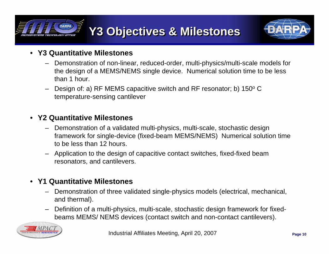
Y3 Objectives & MilestonesY3 Objectives & Milestones• Y3 Quantitative Milestones
– Demonstration of non-linear, reduced-order, multi-physics/multi-scale models for the design of a MEMS/NEMS single device. Numerical solution time to be less than 1 hour.
– Design of: a) RF MEMS capacitive switch and RF resonator; b) 150o C temperature-sensing cantilever
• Y2 Quantitative Milestones– Demonstration of a validated multi-physics, multi-scale, stochastic design
framework for single-device (fixed-beam MEMS/NEMS) Numerical solution time to be less than 12 hours.
– Application to the design of capacitive contact switches, fixed-fixed beam resonators, and cantilevers.
• Y1 Quantitative Milestones– Demonstration of three validated single-physics models (electrical, mechanical,
and thermal). – Definition of a multi-physics, multi-scale, stochastic design framework for fixed-
beams MEMS/ NEMS devices (contact switch and non-contact cantilevers).

Page 11Industrial Affiliates Meeting, April 20, 2007
Model Validation with Experimental Data
Physics-based Model Formulation
Methodology for Methodology for PhysicsPhysics--based Model based Model
DevelopmentDevelopment
Extensive Characterization of Test Structures
Design of Appropriate Test Structures in
Support of DOE for a Given Physical Phenomenon
Definition of Design of Experiments
to Capture Physical Phenomena
DevicePerformance
Definition
Year 1
ExperimentalInvestigation ofGoverning PhysicalPhenomena
Model Development& Validation

Page 12Industrial Affiliates Meeting, April 20, 2007
Questions for the Scientific Advisory Board
• As every research activity, the scientific activity is expected to evolve as new discoveries are made. Currently the IMPACT Center activity is organized by MEMS-device class (i.e. contacting switches)Question: In the long run, how should we reorganize the IMPACT Center technical activity to ensure continuing progress and effective transitioning of the knowledge into practice, to achieve the vision of the Center?
• We are conscious of the fact that our research activities do not encompass all issues that could, in principle, be pursued, given the PIs expertise and interests
• Question: Are there pressing research questions pertinent to the Center’s mission that we must address over the next two years?

Page 13Industrial Affiliates Meeting, April 20, 2007
Questions for theIndustrial Advisory Board
• Our experimental work contributes to the better understanding of the mechanisms responsible for MEMS performance degradation– In addition to improved models, this understanding maps onto
opportunities for improved designs, better manufacturing practices, and even new MEMS-enabled devices
Question: How do we motivate industry input toward the development of new IP?
• Our long-term success is critically dependent on our ability to engage more EDA companies in our Center’s model development activities Question: How can our industry members help us with establishing strong working relationships with EDA Companies?

Page 14Industrial Affiliates Meeting, April 20, 2007
Agenda
8:30 – 9:00 am Registration – Coffee
9:00 – 9:15 Welcome and Introductions
9:15 – 9:30 IMPACT Center Overview
9:30 – 10:15 Thrust 1. Physics of Failure of Contacting MEMS Devices
10:15 – 10:45 Coffee Break
10:45 – 11:30 Thrust 2. Physics of Failure of Non-Contacting MEMS Actuators
11:30 – 12:00 Parallel Sessions: Industry Partner Caucus Scientific Advisory Board Caucus
12:00 – 12:30 pm Feedback to PIs
12:30 – 1:30 Lunch

Page 1April 20, 2007
Thrust 1
Physics of Failureof
Contacting MEMS Devices

Page 2April 20, 2007
Thrust 1: Contacting MEMS Devices
• Objectives:– Develop an improved
understanding of the fundamental science governing the operation of MEMS/NEMS devices which make contact
– Implement this understanding into physics-based models that emulate the underlying principles and allow extrapolation of performance and lifetime improvements
– Validate both the physics and resulting models with test structures and actual switches (and later in phase shifters and antenna subarrays)
-1
-0.5
0
0.5
1
0 100 200 300 400 500TIME (s)
CU
RR
ENT
(pA
)
-20
0
20
40
60
VOLT
AG
E (V
)
30 V off
30 V on
-1
-0.5
0
0.5
1
0 100 200 300 400 500TIME (s)
CU
RR
ENT
(pA
)
-20
0
20
40
60
VOLT
AG
E (V
)
30 V off
30 V on
Mechanical, Mechanical, material, and material, and electricalelectricalpropertiesproperties
PhysicsPhysics--based based and equivalent and equivalent circuit modelscircuit models
Fabricated test Fabricated test structures and structures and switchesswitches

Page 3April 20, 2007
Y1 Milestones/Thrust 1 TasksY1 Milestones/Thrust 1 Tasks
Year 1 Milestones– Demonstration of
three validated single-physics models (mechanical, electrical, and thermal)
– Definition of a multi-physics, multi-scale, stochastic design framework for fixed-beams MEMS/ NEMS devices
Thrust 1 TasksTask 1.1: Fundamentals of material and structural effects and validated models for contacting MEMSTask 1.2: Fundamentals of electrostatic effects and dielectric charging in contacting MEMS Task 1.3: Multi-physics/multi-scale models and design framework for contacting MEMS
-0.6
0
0.6
1.2
0 200 400 600 800TIME (s)
CU
RR
ENT
(pA
)
Positive Charging Discharging
20V30V
40V50V
-0.6
0
0.6
1.2
0 200 400 600 800TIME (s)
CU
RR
ENT
(pA
)
Positive Charging Discharging
20V30V
40V50V

Page 4April 20, 2007
Thrust 1 Progress Overview
• Fabrication/Test Bed (J. Papapolymerou)– Completed design and layout of mask set of mechanical and electrical
test structures for device characterization– Completed first round of fabrication, passed along devices for testing
• Electrical Single-Physics (J. Hwang)– Completed detailed charging characterization of first silicon nitride
samples– Extracted model parameters, including time constants, densities, and
voltage dependence• Material/Mechanical Single-Physics (R. Vinci)
– Established Ansys mechanical models for switch test structures– Completed first set of time-dependant modulus measurements on gold
test samples• Modeling Framework (N. Aluru)
– Initial framework established for multi-physics simulation of mechanical, electrical, and fluidic domains
– Initial results derived for simple test structure-type examples

Page 5April 20, 2007
Multi-physics/multi-scale design framework Validation of physics-based models for contact switch
Electrical, and mechanical characterization
Fabrication of test structures
Design of contact switch mask
SepAugJulJunMayAprMarFebJan
Thrust 1: Schedule
Schedule (1/07-8/07)Month
Task
Phase IMilestone
Phase IMilestone

Page 1
Thrust 1
Development of MEMS/MIM Structures &Initial Study of Dielectric Charging
John PapapolymerouGeorgia Institute of Technology

Page 2
Thrust 1: Facilities
Microelectronics Research Center: Approximately 8,000 sq.ft. of cleanroom areasproviding complete microfabrication capabilities
Main Fabrication Services Include:• Substrate Cleaning• Deposition• Doping• Etching• Lithography (regular + e-beam)• Thermal Processing• Metrology• Mask Design and Production
Measurement Capabilities:• 15,000 sq.ft.• S-parameters (40MHz-110 GHz)• Load-Pull (20 GHz)• Noise (20 GHz)• Antenna Chamber• I-V, C-V MEMS• High Temperature, Cryogenic
High Frequency Lab Management
dc Testing
ac Testing
RF Noise Testing
Load-Pull Testing
Multi-Gigabits Testing
Cryogenic Testing
Infra-Red Testing
Antenna Testing
HF Noise System(2-26GHz)
S-Parameters System(0.045-50GHz)
S-Parameters System(2-110GHz)
Load-Pull System(0.8-18GHz)
RF Cryogenic Chamber(18-350K)
LF Noise System
Load-Pull System(1.8-18GHz)
Echo-Chamber
Multi-gigabits serial datacom itemTesting bench
S-Para. System(4-port / 50GHz)
Prototyping Station
HF Lab Management

Page 3
Thrust 1: Facilities
RF MEMS Testbed: C-V/I-V set-up

Page 4
Thrust 1: Fabrication of Test Structures
E-beam evaporate & pattern gold seed layer
Silicon Nitride Photoresist
Deposit & pattern Silicon Nitride (or Oxide)
RIE of Silicon Nitride and PR removal
PhotoresistGold
E-beam evaporate gold bridge seed layer
Photoresist
Patterning of sacrificial layer (photoresist)
Photoresist
Gold
Photoresist
Patterning of 4th PR layer & Au electroplating
PhotoresistGold
Remove PR & chemical etch of bridge seed layer
Strip photoresist and CO2 release
E-beam evaporate & pattern gold seed layer
Silicon Nitride PhotoresistSilicon Nitride Photoresist
Deposit & pattern Silicon Nitride (or Oxide)
RIE of Silicon Nitride and PR removal
PhotoresistGold
E-beam evaporate gold bridge seed layer
PhotoresistGold
E-beam evaporate gold bridge seed layer
Photoresist
Patterning of sacrificial layer (photoresist)
Photoresist
Patterning of sacrificial layer (photoresist)
Photoresist
Gold
Photoresist
Photoresist
Gold
Photoresist
Patterning of 4th PR layer & Au electroplating
PhotoresistGold
Remove PR & chemical etch of bridge seed layer
PhotoresistGold
Remove PR & chemical etch of bridge seed layer
Strip photoresist and CO2 releaseStrip photoresist and CO2 release
Capacitive RF MEMS Switch Fab Process

Page 5
Thrust 1: Fabrication ofTest Structures
Mask Layout• Mask 1 (Mechanical Mask)
– Mechanical/material test structure (top)
• Mask 2 (Switch Mask)– RF MEMS switches– Switch test structures– TRL calibration structures– Capacitor structures– Stress structures– Thickness structures– Resistivity structures– Mech/material test structure
(bottom)

Page 6
Thrust 1: Fabricated Samples forElectrical Characterization

Page 7
Fabrication Details for Switches/Capacitors:• SixNy with thickness of 200 nm and 400 nm• Metalization: Gold and Aluminum• Various switch geometries (meander, bow-tie etc.)• High temperature issue during evaporationcycle led to switch failure
• Issue is currently being addressedwith assistance from cleanroom staff• MIM capacitors ok• Older switches with 200nm thick
nitride ok
Thrust 1: Fabricated Samples forElectrical Characterization

Page 8
Thrust 1: Investigation ofDielectric Charging
Contact-less charging• Dipoles orientation, produced by rotation of
charges or migration of charges• Space charge (intrinsic) arising from
redistribution of pre-existing and/or filed generated charge carriers
Contacted charging• Space charge (extrinsic) arising from charges
injected into dielectric through various mechanisms
Dipoles
Space charge
Space charge, injected charges
Space charge
Dipoles
Physics of the Dielectric-Charging

Page 9
Thrust 1: Investigation ofDielectric Charging
Contact-less charging
ΔV -ΔV +
Charge build-up induced C-V hysterisis
• Charge build-up at dielectric surface increases the charge of suspended electrode
• As a result the electrostatic force increases with time, hence the capacitance
• The C-V characteristic will exhibit a hysterisis
• The bias for capacitance minimum indicates the sign of dielectric surface charge
• Opposite polarity of bias voltage for capacitance minimum
G. Papaioannou, G. Wang, D. Bessas and J. Papapolymerou in EuMW 2006
-40 -30 -20 -10 0 10 20 30 40
0.2
0.4
0.6
0.8
1.0
1.2
1.4
1.6
C
[
pF]
V [V]
T = 300K
Charge build-up induced C-V hysterisis
Contacted charging
G. Papaioannou, M. Exarchos, V. Theonas, G. Wang and J. Papapolymerou, IEEE MTT 53, 3467, (2005)

Page 10
Summary/Future Work
• Developed first set of MEMS/MIM and mechanical structures for gold metalization
• Initial study of dielectric charging effect based on C-V characteristics
• Complete fabrication of MEMS switches and MIMs for 200 nm/400 nm of SixNy and possibly other dielectric materials for both gold and Aluminum metals
• Electrical characterization (C-V) for MEMS switches under different temperatures for model extraction

Page 2April 20, 2007
Objective ofElectrical Characterization
• Leverage methodology developed under HERMIT program to separate top and bottom charging of dielectric
• Extract trap densities and charging/ discharging time constants from transient current and capacitance measurements on capacitive test structures
• Validate charging model on MEMS switches
• Extrapolate charging model for different control-voltage waveforms and temperatures
• Extend understanding and model to different metal/dielectric combinations
DIELECTRIC
TOP METAL ELECTRODEC
ON
TRO
L VO
LTA
GE
BOTTOM METAL ELECTRODE
DIELECTRIC
TOP METAL ELECTRODEC
ON
TRO
L VO
LTA
GE
0.001
0.01
0.1
1
10
0 100 200 300 400 500
TIME (s)
CU
RR
ENT
(pA
)
20 V
30 V
40 V Discharging
Charging
0.001
0.01
0.1
1
10
0 100 200 300 400 500
TIME (s)
CU
RR
ENT
(pA
)
20 V
30 V
40 V Discharging
Charging
1 10 100 100060
61
62
63
64
65PositiveNegative
Δ C
[fF]
t [sec]

Page 3April 20, 2007
Electrical Test Structures
LPCVD SiO2,, 6µm
Plated Au, 1µm
Evaporated Ti/Au/Ti, 0.2µm
Air, 1.7µm
PECVD SiN, 0.45µmTi/Au, 0.2µm
300µmSwitch Cross Section
@ 100:1 aspect ratio
Test Capacitors

Page 4April 20, 2007
-1.5
-1
-0.5
0
0.5
0 200 400 600 800TIME (s)
CU
RR
ENT
(pA
)
-0.5
0
0.5
1
1.5
0 200 400 600 800TIME (s)
CU
RR
ENT
(pA
)Charging/Discharging of
500µm x 500µm Capacitors
0 01,2
exp( / )[1 exp( / )]exp( / )J J J JON C OFF D
J
Q Q V V t tτ τ=
= − − −∑
Charging
50V40V30V20V
Discharging
Charging Discharging
−20V−30V−40V−50V
Page 5April 20, 2007
1.0E+09
1.0E+10
1.0E+11
1.0E+12
-60 -30 0 30 60
CONTROL VOLTAGE (V)
Q0
(q/c
m2)
0
100
200
300
-60 -40 -20 0 20 40 60
CONTROL VOLTAGE (V)
TIM
E C
ON
STA
NT
(s)
Time & Voltage Dependence
Positive Voltage
J Q00+ (q/cm2) V0+ (V) τC+ (s) τD+ (s)
1 2 x 10⁹ 17 11 18
2 3 x 10⁹ 16 85 178
Negative Voltage
J Q00− (q/cm2) V0− (V) τC− (s) τD− (s)
1 - 2 x 10⁹ 20 11 15
2 - 4 x 10⁹ 16 88 172
(□)τC1 (х)τD1 (Δ)τC2 (+)τD2
QO2+
QO1+
QO2−
QO1−

Page 6April 20, 2007
-1.5
-1
-0.5
0
0 100 200 300 400
TIME (s)
CU
RR
ENT
DEN
SITY
(µA
/cm
2 )
-0.4
-0.2
0
0 100 200 300 400
TIME (s)
CU
RR
ENT
(pA
) 2
2
2
2
Uniformity and Scaling
−30V Charging −70V Charging

Page 7April 20, 2007
• Dielectric charging study methodology developed under HERMIT program appears to be applicable to present samples
• Charging model parameters such as steady-state charge density, time constants, and voltage dependence extracted from metal-insulator-metal capacitors
• Next quarter – 1) use the extracted charging model to predict actuation-voltage shift of switches, 2) validate model on switches, 3) asses top vs. bottom charging of switches, and 4) repeat on more wafers
Summary ofElectrical Characterization

Page 1April 20, 2007
Task 1.1: Fundamentals of material and
structural effects and validated models for
contacting MEMS
X. Yan, B. Baloglu
R.P. Vinci, W.L. Brown, H.F. Nied

Page 2April 20, 2007
Goals and Approach
1.1 Mechanical
testing and
modeling
1.3 Finite
Element
Modeling
1.2 Electrostatic
testing and
modeling DIELECTRIC
BOTTOM ELECTRODE
AIR
POST POST
TOP ELECTRODE
MOVABLE MEMBRANE
HINGE HINGE
Combined electrostatic and
mechanical structures, leading to
validated physics-based models
Goal: characterize coupled mechanical and dielectric charging contributions to stiction
failure; develop and validate physics-based models for test structures and real switches

Page 3April 20, 2007
1.1 Mechanical testing
2cm
Si :730µm
SiNx : 210nm
SiNx : 210nm
After metal deposition:
Au or Al
SiNx membrane : 2 ! 12 or 3 ! 12 mm
KOH etch
Retain nitride membrane during
testing for integrity and to allow
metal compressive residual stress
Strip backside nitride to create
freestanding metal film for
separation of interface effects on
behavior (film must be pinhole
free and tensile)
Mechanical test
specimen fabrication:
Intention: approximate electrostatic load & uniaxial strain with pressure load and
pseudo-uniaxial strain to allow purely mechanical test of time-dependent behavior
N2 gas
Metal plategap
Bulge height increases & capacity
increases; center region is under
approximately uniaxial strain

Page 4April 20, 2007
Load-unload cycles
MPa
GPaE
comp
comp
1.40
6.94
)(0
)(
=
=
!
MPa
GPaE
Au
Au
4.16
6.68
)(0
)(
!=
=
"

Page 5April 20, 2007
Au stress relaxation
Keep strain = 0.00248 tfinal ! 11 hours
E(t ) = 70.888 + 3.7326e(
!t
3367.6)
+ 1.8563e(
!t
151.71)
+ 0.71619e(
!t
7.4307)
+ 0.71619e(
!t
7.3974)
Effect is larger for Al, and larger
at elevated temperatures

Page 6April 20, 2007
1.3 Viscoelastic model
Si Substrate
Post Post
tm
tox
tetd
g0
MembraneSi3N4
Lower ElectrodeSiO2
Si Substrate
Post Post
tm
tox
tetd
g0
MembraneSi3N4
Lower ElectrodeSiO2
Intention: develop and validate models for mechanical and electrostatic pull-down and
release behaviors

Page 7April 20, 2007
Viscoelastic results
UY vs Time
-6.00E-08
-5.50E-08
-5.00E-08
-4.50E-08
-4.00E-08
-3.50E-08
-3.00E-08
-2.50E-08
-2.00E-08
-1.50E-08
-1.00E-08
-5.00E-09
0.00E+00
0 10 20 30 40 50 60
Time
UY
Held for 10s Held for20s Held for 30s Held for 60s Held for 300s
• Relaxation behavior (60 seconds) for different hold times
• Associated with reduced pull-off force, enhanced stiction

Page 8April 20, 2007
Real Membrane Designs
Photos taken from switch samples tested in the Compound
Semiconductor Technology Laboratory at Lehigh University

Page 9April 20, 2007
Linear Elastic Displacements
Membrane-1 Membrane-2 Membrane-3
Membrane-4Membrane-5 Membrane-6

Page 10April 20, 2007
Resultant Forces
9382.202.061AuMembrane-6 (M-6)
362.200.0791AuMembrane-5 (M-5)
1842.200.411AuMembrane-4 (M-4)
442.200.0961AuMembrane-3 (M-3)
4000.960.381AuMembrane-2 (M-2)
1141.120.130.3AlMembrane-1 (M-1)
FAvarage (N/m2)A (m2 x10-8)Ftotal (Nx10-5)tm (µm)Mat.
Calculated Pull-down Forces for each Membrane Geometry
Assumes linear elasticity

Page 11April 20, 2007
Issues/Improvements
• Successes
– 1.1: Initial mechanical structures fabricated at Lehigh and GA Tech
– 1.1: Initial combined structures fabricated at GA Tech
– 1.1: Initial room temperature measurements of Lehigh gold
– 1.1 & 1.3: Transfer of viscoelastic model to Task 1.3
– 1.3: viscoelastic modeling of simple structure
– 1.3: linear elastic modeling of realistic structures
• Sample fabrication across facilities has had growing pains, newfabrication approach conceived
• Mechanical testing upgraded for true constant strain
• Temperature control capability being added to mechanical test
• Finite Element Modeling along two separate paths (simplegeometry/complex physics & reverse)
– Currently combining models to allow use of viscoelastic mechanicalmeasurements for analysis of real structures

Page 12April 20, 2007
Plans for Next Quarter
• Deposition of Al alloys by MEMtronics
• Deposition of Au at GA Tech and Purdue
• Extensive mechanical testing of Lehigh,
GA Tech, and Purdue gold
• Coupling between viscoelastic
measurements and realistic FE modeling
• Initial electrostatic measurements of hybrid
test structure

Page 1April 20, 2007
Computational Framework for Multi-Physics Multi-Scale Modeling
N. Aluru, A.C. Cangellaris

Page 2April 20, 2007
Multi-Physics Modeling
• Lagrangian framework for mechanical, electrical and fluidic energy domains• No mesh movement
• Fast computational methods• Full Newton methods: all cross-coupling terms are computed
accurately enhancing convergence• Efficient stochastic modeling to account for fabrication process induced
variations and uncertainties in model parameters• Uncertainties in mechanical energy domain
• Material properties (e.g. Young’s modulus, Poisson ratio, etc.)• Geometry (roughness, gaps, non-uniformity, etc.)• Noise in applied signals, boundary conditions
• Uncertainties in electrostatic energy domain• Material properties (e.g. dielectric constant)• Geometry (roughness, gaps, etc.)• Applied electrical potentials
• Design iteration-oriented macromodel generation through model order reduction
Desirable Attributes

Page 3April 20, 2007
Coupled Electrostatic-Mechanical Modeling of Capacitive Switch
• Model development based on experimentally-obtained understanding and data
• Coupled electro-mechanical modeling• Incorporate modeling of dielectric charging
• Comprehensive geometry/material modeling• Inhomogeneous domains favor a a finite element-based model
• Explore ways to enhance efficiencyof numerical solution • Lagrangian framework• Equivalent electrostatic problem• Algebraic multigrid solver for electrostatic and mechanical domains

Page 4April 20, 2007
Equivalent Electrostatic Problem (1)
Initial position of top surface
x
Bottom electrode (ground)
Equipotential surface: V0
x0
L1(x0)Top electrode
Flux lines are perpendicular to the two electrodes
L2(x0)
Mathematical non-equipotential surface Sf
xV(x0)
Bottom electrode (ground)
1 0 2 00 0
2 0
( ) ( )( )( )
L x L xV x VL x+
≈
Physical Domain
Equivalent Problem

Page 5April 20, 2007
Equivalent Electrostatic Problem (2)
Advantages:
• Grid remains constant, so no mesh updates needed
• Enhances efficiency of multigrid/iterative solution
• Facilitates coupling with mechanical modeling tool
2d
0 d
( , ) 0 in ( ) on
x yx Vφ
φ∇ = Ω
= Γ
20
0
( , ) 0 in ( ) ( ( )) on
x yx V u xφ
φ∇ = Ω
= Γ
Electrostatic Problem on Deformed Domain Equivalent Problem on Fixed Domain
ΓdΓ0
u(x)

Page 6April 20, 2007
Equivalent Electrostatic Problem (3)
Validation Study 1: Cantilever MEMS SwitchDimensions (μm)bl = 150bh = 2.0gap = 4.5gl = 90gh = 1.5
Tip deflection (microns)
-1.1872-1.1479120-0.5519-0.556390-0.2253-0.228960
Equivalent BVPANSYSVoltage
(V)

Page 7April 20, 2007
Equivalent Electrostatic Problem (4)
Validation Study 2: RF MEMS Capacitive Switch
Dimensions (μm)Lupper = 300t = 0.8g0 = 3.15td = 0.15Llower = 100tm = 0.8tox = 0.4

Page 8April 20, 2007
On-going Activities
• Demonstration of transient coupled electrical-mechanical simulation (June 2007)
• Incorporation of dielectric charging physics model in the coupled electrical-mechanical simulation (August 2007)

Page 1Industrial Affiliates Meeting, April 20, 2007
Thrust 2Thrust 2
Physics of Failure of
Non-contacting, Large Displacement MEMS/NEMS Actuators
Page 2Industrial Affiliates Meeting, April 20, 2007
Thrust 2: Non-ContactingMEMS/NEMS Actuators
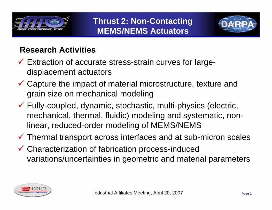
Extraction of accurate stress-strain curves for large-displacement actuatorsCapture the impact of material microstructure, texture and grain size on mechanical modelingFully-coupled, dynamic, stochastic, multi-physics (electric, mechanical, thermal, fluidic) modeling and systematic, non-linear, reduced-order modeling of MEMS/NEMSThermal transport across interfaces and at sub-micron scales Characterization of fabrication process-induced variations/uncertainties in geometric and material parameters
Research Activities

Page 3Industrial Affiliates Meeting, April 20, 2007
Conventional MEMS ActuatorsDesign Methodology
Assumed Material Assumed Material PropertiesProperties
Deterministic Deterministic MultiMulti--Physics Physics
ModelingModeling
Device PerformanceDevice Performance
Device Device Model Model
Questionable Questionable Agreement Agreement
between models between models and experimentsand experiments
Series of unquantifiable hypotheses and “best guesses” for actualmaterial and geometricproperties

Page 4Industrial Affiliates Meeting, April 20, 2007
Thrust-2 New Design Methodology
Probability of Probability of Device FailureDevice Failure
Assumed Material Assumed Material PropertiesProperties
Deterministic Deterministic MultiMulti--Physics Physics
ModelingModeling
Device PerformanceDevice Performance
InIn--situ situ extracted extracted
material and material and geometrical geometrical propertiesproperties
Stochastic Stochastic Models for Models for Materials Materials StructureStructure
Device Device Model Model
Good Agreement Good Agreement between models between models and experimentsand experiments

Page 5Industrial Affiliates Meeting, April 20, 2007
Objectives/Milestones
• Y1 Quantitative Milestones– Demonstration of validated single-physics models
(mechanical, and thermal). – Definition of a multi-physics, multi-scale, stochastic design
framework for non-contact MEMS actuators.
40%60%Thermal Domain
60%50%Uncertainty Quantification
40%70%Mechanical Domain
Modeling EffortsCompleted for Y1
Experimental EffortsCompleted for Y1
Current Status (April 2007)

Page 6Industrial Affiliates Meeting, April 20, 2007
Accomplishments to Date
Strain Rate Dependence of Mechanical Behavior of Metallic MEMS (Au and Pt). Models incorporating these results are currently under development.
Uncertainty modeling of microstructures with fast and accurate methods initiated. Experimental efforts that focus on characterizing the fabrication process uncertainties is currently underway.
Thermal transport model across interfaces and at sub-micron scales initiated. Experimental effort to support this activity is currently underway.
Page 7Industrial Affiliates Meeting, April 20, 2007
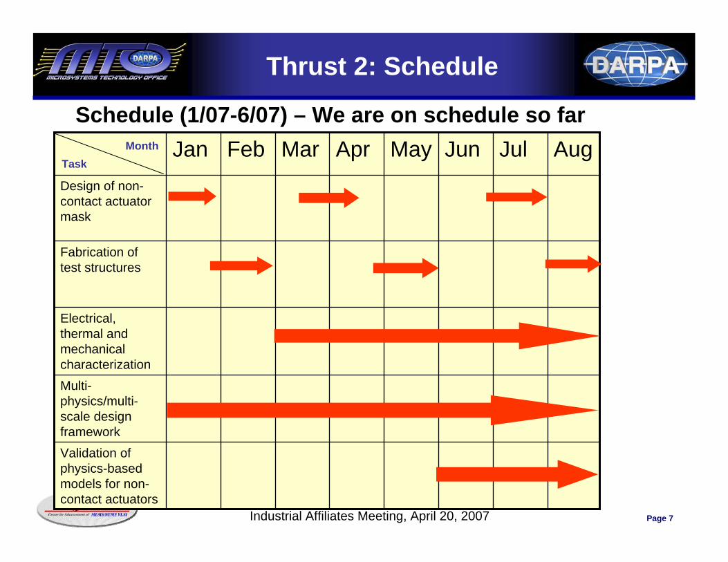
Multi-physics/multi-scale design framework Validation of physics-based models for non-contact actuators
Electrical, thermal and mechanical characterization
Fabrication of test structures
Design of non-contact actuator mask
AugJulJunMayAprMarFebJan
Thrust 2: Schedule
Schedule (1/07-6/07) – We are on schedule so farMonth
Task

Page 8Industrial Affiliates Meeting, April 20, 2007
Mechanical Behavior Experiments and ModelsX. Tang, K. Jonnalagadda, I. Chasiotis, P. Geubelle
Aerospace Engineering, University of Illinois at Urbana-Champaign
Sample Fabrication D. Peroulis1, R. Polcawich2
1Purdue University, 2Army Research Laboratory, Adelphi, MD
Strain Rate Dependence of MechanicalBehavior of Metallic MEMS
Acknowledgements:DARPA IMPACT Center, Program Manager: Dr. D. Polla
ARO, Program Manager: Dr. B. LaMattina
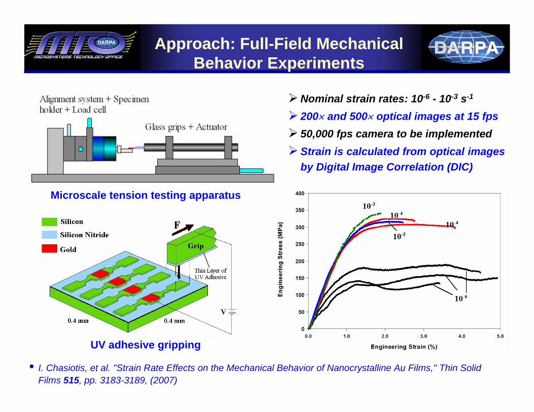
Page 9Industrial Affiliates Meeting, April 20, 2007• I. Chasiotis, et al. "Strain Rate Effects on the Mechanical Behavior of Nanocrystalline Au Films," Thin Solid
Films 515, pp. 3183-3189, (2007)
Microscale tension testing apparatus
UV adhesive gripping
Nominal strain rates: 10-6 - 10-3 s-1
200× and 500× optical images at 15 fps50,000 fps camera to be implementedStrain is calculated from optical images by Digital Image Correlation (DIC)
Approach: Full-Field MechanicalBehavior Experiments

Page 10Industrial Affiliates Meeting, April 20, 2007
Sample dimensions: L= 1000 μmT= 400 nmW= 100-200 μm
Specimen grip
Specimen Preparation and Geometry

Page 11Industrial Affiliates Meeting, April 20, 2007
100 μm 100 μm
Strain Measurement - Digital Image Correlation (DIC)
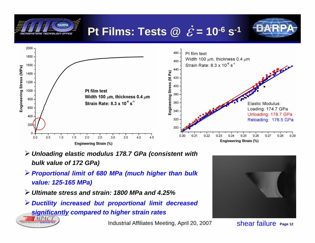
Page 12Industrial Affiliates Meeting, April 20, 2007 shear failure
Unloading elastic modulus 178.7 GPa (consistent with bulk value of 172 GPa)Proportional limit of 680 MPa (much higher than bulk value: 125-165 MPa)Ultimate stress and strain: 1800 MPa and 4.25%Ductility increased but proportional limit decreased significantly compared to higher strain rates
Pt Films: Tests @ = 10-6 s-1ε&

Page 13Industrial Affiliates Meeting, April 20, 20071405
1490
1537
1541
1640
Yield stress (MPa)
4.2%1800680178.78.3 x 10-65
4.3%1920720181.88.3 x 10-54
3.9%1870904173.17.0 x 10-43
4.0%1870876173.87.1 x 10-42
3.4%19901000186.73.6 x 10-31
Ultimate strain
UTS (MPa)Proportional limit (MPa)
E (GPa)Strain rate (s-1)Pt
Effect of Strain Rate on Mechanical Behavior of Pt Films

Page 14Industrial Affiliates Meeting, April 20, 2007
Elastic modulus E= 178.3 ± 6.2 GPa was not affected by the strain rateTensile strength increased marginally with strain rate (1800-2000 MPa) and was significantly larger than bulk (~240 MPa), which is potentially a consequence of limited defect density in the filmsThe proportional limit decreased by more than 30% in the entire strain range
Ductility changed by 20% between 10-6 to 10-3 s-1
Tensile Properties of Pt Films

Page 15Industrial Affiliates Meeting, April 20, 2007
Tensile Response of Notched Pt Film

Page 16Industrial Affiliates Meeting, April 20, 2007
500 x Magnification
CPW Au: Width 50 μm, thickness 1.2 μm
Test of SiO2 - Au Films

Page 17Industrial Affiliates Meeting, April 20, 2007
Multiscale Modeling of Damage in MEMS
Objective: Multiscale framework to relate grain-level damage evolution (Experiments by I. Chasiotis) to macroscale performance of MEMS (Experiments by D. Peroulis and simulations by N. Aluru)
Approach: Mathematical theory of homogenization, based on asymptotic expansion of stress and strain fields
Current activities:
Generation of realistic granular microstructure using and experimental inputs (texture data from I. Chasiotis) Voronoitessellation
Multiscale prediction of elastic properties

Page 18Industrial Affiliates Meeting, April 20, 2007
Implemented a method (with Pt films) and test apparatus to measure full field strains with optical microscopy and at a variety of strain rates relevant to MEMS operation
The mechanical response of Pt samples was measured at 4 strain rates and the elastic modulus, elastic limit, and ductility were computed
Pt films were less susceptible to strain rate compared to Au films tested in the past
Deformation and failure of Pt was due to micro-plasticity without the formation of shear bands (contrary to Au)
Decreasing loading rate resulted in 40% reduction in the elastic limit of Pt
The elastic range of Pt films was 0.4%. In comparison, the elastic limit of Au/SiO2 films was less than 0.1%: rather small given common operating and thermal loading conditions
Concluding Remarks

Page 19Industrial Affiliates Meeting, April 20, 2007
Uncertainty ModelingN.R. Aluru, A. Cangellaris
University of Illinois at Urbana-Champaign

Page 20Industrial Affiliates Meeting, April 20, 2007
Uncertainties or stochastic parameters are variations in the physical quantities that are important for device function
ExamplesUncertainties in geometrical features such as dimensions, gap between electrodes, etc.Uncertain operating environments (e.g. temperature, pressure, fluctuations in applied volatges, etc.)Uncertainties in material and physical properties can be significantFabrication errors can lead to imperfect contacts and uncertainties in boundary conditions
Uncertainties

Page 21Industrial Affiliates Meeting, April 20, 2007
Why are uncertainties important?Reliability, failure and life-cycle tests can not be quantified with out accounting for uncertaintiesDevices can fail sooner than expectedDevices can operate in a different regime than what they were designed/intended for (e.g. chaotic behavior, nonlinear regime, etc.)
Uncertainties
Design for worst caseVery conservative approachCan be quite expensive, inefficientDesigners would like to do better!
Standard approaches for uncertainty quantificationMonte Carlo methods (expensive)Sensitivity analysis (limited to small variations)Perturbation methods (limited to small variations)

Page 22Industrial Affiliates Meeting, April 20, 2007
Important variationsMechanical properties (e.g. Young’s modulus, Poisson’s ratio)Physical properties (e.g. thermal conductivity, electrical conductivity, diffusion coefficients, etc.)GeometryBoundary conditions (imperfect metal contacts, fluctuations in the applied voltages, etc.), residual stresses, etc.
UQ in MEMS
ApproachExtend our earlier research on deterministic analysis of electrostatic MEMS (coupled electrostatic and mechanical domains) to account for uncertaintiesInvestigate the effect of uncertainties in material properties in mechanical analysisUncertainties in mechanical properties lead to uncertain displacementsInvestigate the effect of uncertain geometries in electrostatic analysisPerform coupled analysis of stochastic mechanical/electrostatic domains

Page 23Industrial Affiliates Meeting, April 20, 2007
Geometrical Uncertainties
Deterministic problem: For a given set of conductors and applied potential difference, compute the surface charge density and the capacitanceStochastic problem: For a given set of conductors with uncertain geometry and applied potential difference, quantify the uncertainty associated with the surface charge density and the capacitance
Approach: Model the uncertain geometry and unknown surface charge density as random fields, which are then expanded in terms of independent random variables using polynomial chaos expansions

Page 24Industrial Affiliates Meeting, April 20, 2007
Deterministic Lagrangian Electrostatics
Lets assume the conductors have undergone some shape changes (e.g. due to electrothermal effects, etc.)In classical electrostatic analysis, we need to solve a potential equation in the domain exterior to all the conductorsAn efficient approach is to use boundary integral equation formulationThe boundary integral equations for electrostatic analysis are given by
Green’s function (2D)
Question: Instead of using the deformed geometry, can we use the original geometry to perform electrostatic analysis?

Page 25Industrial Affiliates Meeting, April 20, 2007
Deterministic Lagrangian Electrostatics
Lagrangian electrostatics: Mathematical transformation to solve the electrostatic equations on the undeformed geometry of the conductors
Lagrangian BIEBoundary integral equations (BIE)
[Li and Aluru, 2002]
Deformed geometry = Undeformed geometry + a displacement at each point

Page 26Industrial Affiliates Meeting, April 20, 2007
Stochastic Lagrangian Electrostatics
Uncertain geometry Mean geometry Uncertain displacement
Stochastic Lagrangian BIE

Page 27Industrial Affiliates Meeting, April 20, 2007
Stochastic Discretization
Input uncertainty:
Using Galerkin projection in the space of PC basic functions :
Discretize in space using Boundary Element Method (BEM)

Page 28Industrial Affiliates Meeting, April 20, 2007
Example: Single Line Over a Ground Plane
Mean: ; Standard deviation
We assume , Gaussian RV
Objective: Study the effect of uncertain gap H on the capacitance between the line and ground plane
Surface charge density profilein the mean configuration
Mean surfacecharge density with error barsat the bottomsurface

Page 29Industrial Affiliates Meeting, April 20, 2007
Example: Single Line Over a Ground Plane
Empirical formula for capacitance:
PDF of capacitance for PC, Emp and MC

Page 30Industrial Affiliates Meeting, April 20, 2007
Example: Comb Drive
Transverse comb drive
Movable tooth Fixed tooth
Effect of uncertain tooth thickness on the capacitance and net electrostatic force
Uncertain displacement :

Page 31Industrial Affiliates Meeting, April 20, 2007
Example: Comb Drive
PDF of capacitance using PC
Mean vertical force with error bars for different applied voltages
Page 32Industrial Affiliates Meeting, April 20, 2007
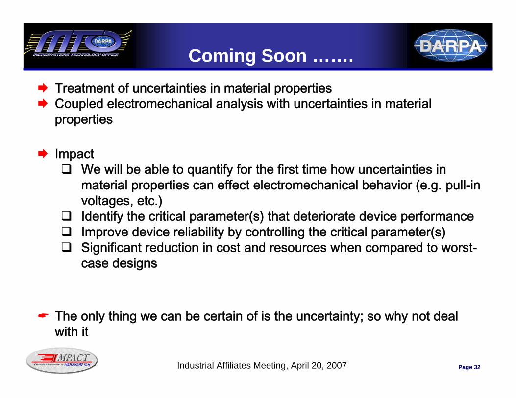
Coming Soon …….Treatment of uncertainties in material propertiesCoupled electromechanical analysis with uncertainties in material properties
The only thing we can be certain of is the uncertainty; so why not deal with it
ImpactWe will be able to quantify for the first time how uncertainties in material properties can effect electromechanical behavior (e.g. pull-in voltages, etc.)Identify the critical parameter(s) that deteriorate device performanceImprove device reliability by controlling the critical parameter(s)Significant reduction in cost and resources when compared to worst-case designs

Page 33Industrial Affiliates Meeting, April 20, 2007
Experimental Investigation of Fabrication Uncertainties: Fast and Accurate Metrology Methods
D. Peroulis, J.V. ClarkSchool of Electical and Computer Engineering, Birck Nanotechnology Center,
School of Mechanical Engineering, Purdue University

Page 34Industrial Affiliates Meeting, April 20, 2007
What are the basic properties of your materials?
How do they vary across your wafer?
How do they vary from run-to-run?
How does your layout compare to the actual fabricated device?
What is the cost (time & $$$) for measuring onegeometrical/material property?
How accurately can you measure your geometrical/materialproperties ?
What is the reliability or failure mechanisms of your devices?
Basic Questions

Page 35Industrial Affiliates Meeting, April 20, 2007
Example: Tang Resonator
Tang Resonator
Example question: How Δw affects performance?

Page 36Industrial Affiliates Meeting, April 20, 2007
Example: Tang Resonator
Δw affects width, gap, length; mass, damping, stiffness; resistance, capacitance; etc.

Page 37Industrial Affiliates Meeting, April 20, 2007
Material UncertaintyPolySi – Most common MEMS material
Various methods and group (year published)
You
ng’s
mod
ulus
of p
olys
ilicon
[GPa
]

Page 38Industrial Affiliates Meeting, April 20, 2007
Relative Error Due to Both Δw and ΔE
Rel
ativ
e er
ror i
n st
iffne
ss

Page 39Industrial Affiliates Meeting, April 20, 2007
What Needs to Be Measured?
Material Propertieso E, vo stresso densityo CTEo piezo coefficiento conductivityo …
Geometric Propertieso length, width, gapo thicknesso displacement/forceo radius of curvatureo …
Material degradationo creepo fatigueo …
Fabrication process variationso run-to-runo across the wafero …
Post-process variationso packagingo flip-chip bondingo …

Page 40Industrial Affiliates Meeting, April 20, 2007
Example Test Structure

Page 41Industrial Affiliates Meeting, April 20, 2007
Example Test Structure
Tensile fracture by W. Sharpe (JHU)
Hypothesis: Fabrication errors are locally identical

Page 42Industrial Affiliates Meeting, April 20, 2007
Derivation of Δw2
, 012
aa eff a a
a
CF k y Vy
Δ= Δ = Δ
Δ2
, 012
bb eff b b
b
CF k y Vy
Δ= Δ = Δ
Δ
1 3
,1 3
1
1
aa layou
b
t
a
b
b
Cn
C
Cw w
C
⎛ ⎞⎛ ⎞⎜ ⎟−⎜ ⎟Δ⎜ ⎟⎝ ⎠Δ = ⎜ ⎟
⎛ ⎞⎜ ⎟−⎜ ⎟⎜ ⎟Δ⎝ ⎠⎝ ⎠
Δ
Δ
,
3,
,
3,
eff a a
a
eff
eff b b
eff
a a
b b
b
k y
yk w
k y
k wy
Δ
Δ
Δ =
⇓
Δ= =
02
02 1
212
b
b
b
a
a
a a
b
CCVy
y
Vy
y CC
ΔΔΔ =
Δ
⇓Δ Δ
=
ΔΔ
Δ Δ
=
Measurement of Δw is in terms of precisely measured capacitanceand exactly known layout parameters.
=
Experiments are underway

Page 43Industrial Affiliates Meeting, April 20, 2007
Systematic Errors: Food for Thought
Ti/SiO2 beams
How can this be modeled?
How can it be experimentally characterized?
Can such effects be used formore robust devices?

Page 44Industrial Affiliates Meeting, April 20, 2007
Thermal ModelingJ. Murthy
School of Mechanical Engineering, Purdue University
U. RavaioliECE Department, University of Illinois

Page 45Industrial Affiliates Meeting, April 20, 2007
Contacting and Non-Contacting MEMS
Contacting MEMS
Non-Contacting MEMS
Complex physics involving coupling of electrical, thermal and mechanical domains
Radant MEMS Memtronics switch Lincoln Lab switch
Pourkamali, et al (2003)

Page 46Industrial Affiliates Meeting, April 20, 2007
Thermal Transport Issues in MEMS
For silicon MEMs structures:– Heat transfer in semiconductors and dielectrics is by phonon transport– When phonon mean free path (~300 nm) becomes comparable to layer
thickness, sub-continuum transport must be considered– Phonon transport across multi-material interfaces poorly understood– Electro-thermal coupling poorly understood
L
Λ<<L
L
Λ>>L
Two regimes, (a) Fourier’s law is valid, (b) Fourier’s law is invalid, Λ is the mean free path of the heat carrier (phonons or electrons)
(a) (b)

Page 47Industrial Affiliates Meeting, April 20, 2007
Heat Transport in Silicon
.
( )scat
f fft t
∂ ∂⎛ ⎞+∇⋅ = ⎜ ⎟∂ ∂⎝ ⎠v
Boltzmann transport equation for phonons:
Phonons are characterized by polarization and dispersion.
Electron-phonon scattering during Joule heating transfers energy to specific phonon groups
MEMs temperature depends on which phonons receive this energy and how fast they move
Efficient solution techniques have been devised to solve BTE
Frequency vs. reduced wave number in (100) direction for silicon
Narumanchi, Murthy and Amon, ASME JHT 2003,2005
Wang and Murthy, ASME IMECE 2006

Page 48Industrial Affiliates Meeting, April 20, 2007
Example: Electrothermal Transportin PD/SOI nMOSFET
STI
BOX
M1
Silicon substrate
Metallization Layers
Kumar, S., Kim, K., Joshi, R. V., Chuang, C. T., and Murthy, J. Y.; Self-Consistent Electro-Thermal Modeling For FinFetTechnologies; ICCAD, San Jose, CA, November 5-9, 2006.Pascual-Gutiérrez, J., Murthy, J.Y., Viskanta R., Joshi, R.V., Chuang,C-T, and Kang, S.S.;Simulation of Nano-Scale Multi-
Fingered PD/SOI MOSFETs using Boltzmann Transport Equation; ASME National Heat Transfer Conference, HT-FED2004-56375, Charlotte, NC, July 2004
ChannelCoupled Fourier and phonon BTE calculations of temperature field in multi-material complex structures.
Heat generation from TAURUS simulation

Page 49Industrial Affiliates Meeting, April 20, 2007
Interface Physics: Acoustic Impedance
B: Heavy atoms (Mass 4M)
A: Light atoms (Mass M)
0.0 0.2 0.4 0.6 0.8 1.00
2
4
6
8
10
12
14
16
2 / aπ
dispersion for A dispersion for B
frequ
ency
(Thz
)wave vector
K/(2π/a)
Freq
uenc
y (T
Hz)
Material B has much lower frequency range. So high-frequency phonons cannot cross from A to B

Page 50Industrial Affiliates Meeting, April 20, 2007
Phonon Transmissivity Across Interface
• Only low-frequency phonons are transmitted
• Only these phonons have a density of states on the heavy side
• High frequency phonons have no counterpart on the heavy side and are reflected
0 2 4 6 8 10 120 .0
0 .1
0 .2
0 .3
0 .4
0 .5
0 .6
0 .7
0 .8
0 .9
1 .0
trans
mis
sion
f re q u e n cy (T H z)
Frequency-dependent transmissivity of LA phonons across interface (Lin and Murthy, 2006)
Tran
smis
sivi
ty
Frequency (THz)
Cut-off

Page 51Industrial Affiliates Meeting, April 20, 2007
Thermal Transport in Metals
• In metals, thermal transport is primarily by free electrons• Thermal and electrical transport are related through the
Wiedemann-Franz Law
• For thin metal films, size effects become important when the carrier mfp (~40nm) competes with layer thickness. A simplified Boltzmann transport equation (BTE) could be used.
• For thicker layers, ohmic conduction may be assumed.• Thermal and electrical conductivity may be found for confined
structures from the BTE.
k: Thermal conductivity
σ: Electrical conductivity
L: Lorenz number
T: Temperature
k LTσ=
Page 52Industrial Affiliates Meeting, April 20, 2007
Electro-Thermal Models
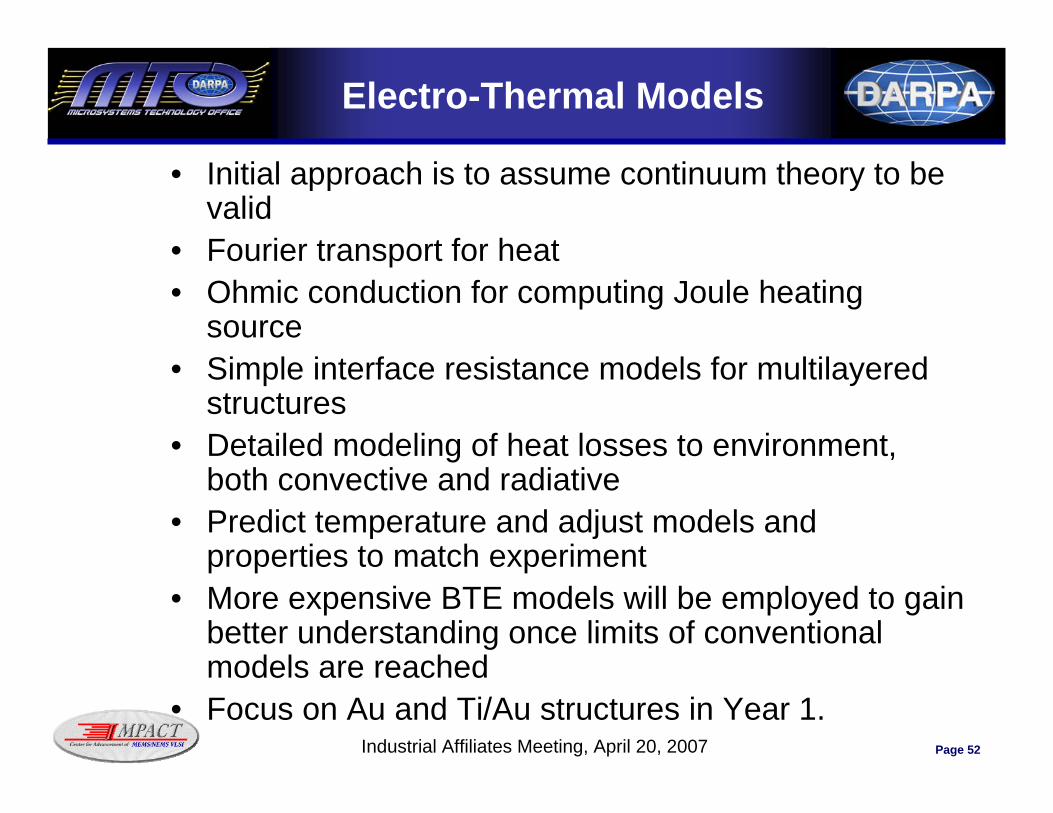
• Initial approach is to assume continuum theory to be valid
• Fourier transport for heat• Ohmic conduction for computing Joule heating
source• Simple interface resistance models for multilayered
structures• Detailed modeling of heat losses to environment,
both convective and radiative• Predict temperature and adjust models and
properties to match experiment• More expensive BTE models will be employed to gain
better understanding once limits of conventional models are reached
• Focus on Au and Ti/Au structures in Year 1.

Page 53Industrial Affiliates Meeting, April 20, 2007
Simulation Approach
• Unstructured, solution-adaptive finite volume scheme widely used for continuum fluid flow and heat transfer simulation
• Fourier conduction & Joule heating in solid layers
• Navier-Stokes and energy equation solution for fluid flow and heat transfer outside
• Gray-diffuse surface-to surface exchange model for radiativeexchange
S.R. Mathur and J.Y. Murthy, Numerical Heat Transfer, Vol. 31, No. 2,1997.
J.Y. Murthy and S.R. Mathur, Journal of Heat Transfer, Vol.120, 1998.

Page 54Industrial Affiliates Meeting, April 20, 2007
Closure
• Thermal modeling of MEMS structures is underway
• Continuum-based models for thermal transport with Joule heating are being completed
• Comparisons with measurements will be completed this summer

Page 55Industrial Affiliates Meeting, April 20, 2007
Questions for the Scientific Advisory Board
• As every research activity, the scientific activity is expected to evolve as new discoveries are made. Currently the IMPACT Center activity is organized by MEMS-device class (i.e. contacting switches)Question: In the long run, how should we reorganize the IMPACT Center technical activity to ensure continuing progress and effective transitioning of the knowledge into practice, to achieve the vision of the Center?
• We are conscious of the fact that our research activities do not encompass all issues that could, in principle, be pursued, given the PIs expertise and interests
• Question: Are there pressing research questions pertinent to the Center’s mission that we must address over the next two years?

Page 56Industrial Affiliates Meeting, April 20, 2007
Questions for theIndustrial Advisory Board
• Our experimental work contributes to the better understanding of the mechanisms responsible for MEMS performance degradation– In addition to improved models, this understanding maps onto
opportunities for improved designs, better manufacturing practices, and even new MEMS-enabled devices
Question: How do we motivate industry input toward the development of new IP?
• Our long-term success is critically dependent on our ability to engage more EDA companies in our Center’s model development activities Question: How can our industry members help us with establishing strong working relationships with EDA Companies?


