37

springer.com
Springer Berlin Heidelberg New York
Nanotechnology
About this bookVolumes II, III and IV examine the physical and technical foundation for recent progress in applied near-field scanning probe techniques, and build upon the first volume published in
early 2004. The field is progressing so fast that there is a need for a second set of volumes to capture the latest developments. It constitutes a timely comprehensive
overview of SPM applications, now that industrial applications span topographic and dynamical surface studies of thin-film semiconductors, polymers, paper, ceramics, and
magnetic and biological materials. Volume II introduces scanning probe microscopy, including sensor technology, Volume III covers the whole range of characterization
possibilities using SPM and Volume IV offers chapters on uses in various industrial applications. The international perspective offered in these three volumes - which belong
together - contributes further to the evolution of SPM techniques.
Written for:
Professionals in industry dealing with surface analytics, scientists at universities in physical chemistry/physics, materials science, polymer science departments
Keywords:
Material Science
Microscopy
Nanoscience
Physical Chemistry
Applied Scanning Probe Methods IIICharacterization
Series: NanoScience and Technology Volume package Applied Scanning Probe Methods
Bhushan, Bharat; Fuchs, Harald (Eds.) 2006, XLIV, 378 p., 270 illus., 2 in colour, Hardcover
ISBN: 978-3-540-26909-0
This item usually ships in 2-3 days.
$169.00

Contents – Volume III
12 Atomic Force Microscopy in NanomedicineDessy Nikova, Tobias Lange, Hans Oberleithner,Hermann Schillers, Andreas Ebner, Peter Hinterdorfer . . . . . . . 1
12.1 AFM in Biological Sciences . . . . . . . . . . . . . . . . . . . . . 1
12.2 Plasma Membrane Preparation for AFM Imaging . . . . . . . . . . 412.2.1 Introduction . . . . . . . . . . . . . . . . . . . . . . . . . . . . . . 412.2.2 Plasma Membrane Preparation . . . . . . . . . . . . . . . . . . . . 512.2.3 Atomic Force Microscopy . . . . . . . . . . . . . . . . . . . . . . 712.2.4 Molecular Volume Measurements of Membrane Proteins . . . . . . 712.2.5 AFM Imaging . . . . . . . . . . . . . . . . . . . . . . . . . . . . . 7
12.3 AFM Imaging of CFTR in Oocyte Membranes . . . . . . . . . . . 1012.3.1 Introduction . . . . . . . . . . . . . . . . . . . . . . . . . . . . . . 1112.3.2 Does the CFTR Form Functional Assemblies? . . . . . . . . . . . 1112.3.3 Two CFTRs are Better Than One . . . . . . . . . . . . . . . . . . . 13
12.4 Single Antibody–CFTR Recognition Imaging . . . . . . . . . . . . 1612.4.1 Introduction . . . . . . . . . . . . . . . . . . . . . . . . . . . . . . 1612.4.2 Tethering of Antibodies to AFM Tips . . . . . . . . . . . . . . . . 1712.4.3 AFM Imaging and Recognition . . . . . . . . . . . . . . . . . . . . 1712.4.4 A Single Antibody Sees a Single CFTR . . . . . . . . . . . . . . . 17
12.5 Single Cell Elasticity: Probing for Diseases . . . . . . . . . . . . . 1912.5.1 Introduction . . . . . . . . . . . . . . . . . . . . . . . . . . . . . . 1912.5.2 Force–Mapping AFM . . . . . . . . . . . . . . . . . . . . . . . . . 2012.5.3 Can One Protein Change Cell Elasticity? . . . . . . . . . . . . . . 21
12.6 Summary . . . . . . . . . . . . . . . . . . . . . . . . . . . . . . . . 24
References . . . . . . . . . . . . . . . . . . . . . . . . . . . . . . . . . . . . 24
X Contents – Volume III
13 Scanning Probe Microscopy:From Living Cells to the Subatomic RangeIlle C. Gebeshuber, Manfred Drack, Friedrich Aumayr,Hannspeter Winter, Friedrich Franek . . . . . . . . . . . . . . . . . 27
13.1 Introduction . . . . . . . . . . . . . . . . . . . . . . . . . . . . . . 27
13.2 Cells In Vivo as Exemplified by Diatoms . . . . . . . . . . . . . . 2813.2.1 Introduction to Diatoms . . . . . . . . . . . . . . . . . . . . . . . . 2813.2.2 SPM of Diatoms . . . . . . . . . . . . . . . . . . . . . . . . . . . . 30
13.3 Interaction of Large Organic Molecules . . . . . . . . . . . . . . . 33
13.4 Nanodefects on Atomically Flat Surfaces . . . . . . . . . . . . . . 3713.4.1 Ion Bombardment of Highly Oriented Pyrolytic Graphite (HOPG) 3813.4.2 Bombardment of Single Crystal Insulators with Multicharged Ions 42
13.5 Subatomic Features . . . . . . . . . . . . . . . . . . . . . . . . . . 4513.5.1 Atom Orbitals . . . . . . . . . . . . . . . . . . . . . . . . . . . . . 4513.5.2 Single Electron Spin Detection with AFM and STM . . . . . . . . 47
13.6 Conclusions and Outlook . . . . . . . . . . . . . . . . . . . . . . . 50
References . . . . . . . . . . . . . . . . . . . . . . . . . . . . . . . . . . . . 51
14 Surface Characterization and Adhesion and Friction Propertiesof Hydrophobic Leaf Surfaces and Nanopatterned Polymersfor Superhydrophobic SurfacesZachary Burton, Bharat Bhushan . . . . . . . . . . . . . . . . . . 55
14.1 Introduction . . . . . . . . . . . . . . . . . . . . . . . . . . . . . . 55
14.2 Experimental Details . . . . . . . . . . . . . . . . . . . . . . . . . 5814.2.1 Instrumentation . . . . . . . . . . . . . . . . . . . . . . . . . . . . 5814.2.2 Samples . . . . . . . . . . . . . . . . . . . . . . . . . . . . . . . . 5914.2.3 Roughness Factor . . . . . . . . . . . . . . . . . . . . . . . . . . . 6114.2.4 Test Matrix for Nanopatterned Polymers . . . . . . . . . . . . . . . 62
14.3 Results and Discussion . . . . . . . . . . . . . . . . . . . . . . . . 6314.3.1 Hydrophobic Leaf Surfaces . . . . . . . . . . . . . . . . . . . . . . 6414.3.2 Nanopatterned Polymers . . . . . . . . . . . . . . . . . . . . . . . 74
14.4 Summary . . . . . . . . . . . . . . . . . . . . . . . . . . . . . . . . 79
References . . . . . . . . . . . . . . . . . . . . . . . . . . . . . . . . . . . . 81
15 Probing Macromolecular Dynamics and the Influenceof Finite Size EffectsScott Sills, René M. Overney . . . . . . . . . . . . . . . . . . . . . 83
15.1 Introduction . . . . . . . . . . . . . . . . . . . . . . . . . . . . . . 84

Contents – Volume III XI
15.2 The Glass Transition and Molecular Mobility . . . . . . . . . . . . 85
15.3 Macromolecular Probing Techniques . . . . . . . . . . . . . . . . 9015.3.1 Static Contacts . . . . . . . . . . . . . . . . . . . . . . . . . . . . . 9015.3.2 Modulated Contacts . . . . . . . . . . . . . . . . . . . . . . . . . . 9215.3.3 Calibration of Lateral Forces in Scanning Probe Microscopy . . . . 9315.3.4 Shear Modulation Force Microscopy (SM-FM) . . . . . . . . . . . 9715.3.5 Friction Force Microscopy (FFM) . . . . . . . . . . . . . . . . . . 9815.3.6 Tribological Models for FFM . . . . . . . . . . . . . . . . . . . . . 99
15.4 Internal Friction and Dynamics near the Glass Transition . . . . . 10315.4.1 Molecular Relaxations . . . . . . . . . . . . . . . . . . . . . . . . 10315.4.2 Structural Heterogeneity and Relaxation near the Glass Transition 10515.4.3 Cooperative Molecular Motion During the Glass Transition . . . . 107
15.5 Constraints and Structural Modifications near Interfaces . . . . . . 10915.5.1 Interfacial Plasticization . . . . . . . . . . . . . . . . . . . . . . . . 10915.5.2 Dewetting Kinetics . . . . . . . . . . . . . . . . . . . . . . . . . . 11015.5.3 Disentanglement Barriers . . . . . . . . . . . . . . . . . . . . . . . 11115.5.4 Interfacial Glass Transition Profiles . . . . . . . . . . . . . . . . . 113
15.6 Mechanical Operations in Nanoscopic Polymer Systems . . . . . . 11515.6.1 Indentation Contact Mechanics . . . . . . . . . . . . . . . . . . . . 11615.6.2 Rim Formation During Indentation . . . . . . . . . . . . . . . . . . 12015.6.3 Strain Shielding and Confined Plasticity
in Nanoscopic Polymer Systems . . . . . . . . . . . . . . . . . . . 122
15.7 Closing Remarks . . . . . . . . . . . . . . . . . . . . . . . . . . . 126
References . . . . . . . . . . . . . . . . . . . . . . . . . . . . . . . . . . . . 127
16 Investigation of Organic Supramolecules by Scanning Probe Microscopyin Ultra-High VacuumLaurent Nony, Enrico Gnecco, Ernst Meyer . . . . . . . . . . . . . 131
16.1 Introduction . . . . . . . . . . . . . . . . . . . . . . . . . . . . . . 131
16.2 Methods . . . . . . . . . . . . . . . . . . . . . . . . . . . . . . . . 13216.2.1 Organic Molecular Beam Epitaxy (OMBE) . . . . . . . . . . . . . 13216.2.2 Scanning Tunneling Microscopy (STM) . . . . . . . . . . . . . . . 13416.2.3 Atomic Force Microscopy (AFM) . . . . . . . . . . . . . . . . . . 137
16.3 Molecules . . . . . . . . . . . . . . . . . . . . . . . . . . . . . . . 14216.3.1 Fullerenes . . . . . . . . . . . . . . . . . . . . . . . . . . . . . . . 14216.3.2 Porphyrins . . . . . . . . . . . . . . . . . . . . . . . . . . . . . . . 14216.3.3 Phthalocyanines . . . . . . . . . . . . . . . . . . . . . . . . . . . . 14216.3.4 Perylene Derivatives . . . . . . . . . . . . . . . . . . . . . . . . . . 14416.3.5 Lander Molecules . . . . . . . . . . . . . . . . . . . . . . . . . . . 14416.3.6 PVBA Molecules . . . . . . . . . . . . . . . . . . . . . . . . . . . 14416.3.7 Decacyclene and Derivatives . . . . . . . . . . . . . . . . . . . . . 144

XII Contents – Volume III
16.4 Molecules on Metals . . . . . . . . . . . . . . . . . . . . . . . . . 14516.4.1 STM Investigations . . . . . . . . . . . . . . . . . . . . . . . . . . 14516.4.2 Non-Contact AFM Investigations . . . . . . . . . . . . . . . . . . 157
16.5 Molecules on Semiconductor Surfaces . . . . . . . . . . . . . . . . 16216.5.1 STM Investigations . . . . . . . . . . . . . . . . . . . . . . . . . . 16216.5.2 Non-Contact AFM Investigations . . . . . . . . . . . . . . . . . . 165
16.6 Molecules on Insulating Surfaces . . . . . . . . . . . . . . . . . . . 16716.6.1 STM Investigations . . . . . . . . . . . . . . . . . . . . . . . . . . 16816.6.2 Non-contact AFM Investigations . . . . . . . . . . . . . . . . . . . 169
16.7 Manipulation of Single Molecules . . . . . . . . . . . . . . . . . . 17116.7.1 STM Investigations . . . . . . . . . . . . . . . . . . . . . . . . . . 17116.7.2 Non-contact AFM Investigations . . . . . . . . . . . . . . . . . . . 175
16.8 Conclusions . . . . . . . . . . . . . . . . . . . . . . . . . . . . . . 175
References . . . . . . . . . . . . . . . . . . . . . . . . . . . . . . . . . . . . 176
17 One- and Two-Dimensional Systems: Scanning Tunneling Microscopyand Spectroscopy of Organic and Inorganic StructuresLuca Gavioli, Massimo Sancrotti . . . . . . . . . . . . . . . . . . . 183
17.1 Introduction . . . . . . . . . . . . . . . . . . . . . . . . . . . . . . 183
17.2 Basic Principles of STM and STS . . . . . . . . . . . . . . . . . . 185
17.3 Inorganic Overlayers . . . . . . . . . . . . . . . . . . . . . . . . . 18817.3.1 1D Structures . . . . . . . . . . . . . . . . . . . . . . . . . . . . . 18817.3.2 2D Structures . . . . . . . . . . . . . . . . . . . . . . . . . . . . . 196
17.4 Molecular Overlayers . . . . . . . . . . . . . . . . . . . . . . . . . 20117.4.1 1D Structures . . . . . . . . . . . . . . . . . . . . . . . . . . . . . 20217.4.2 2D Overlayers . . . . . . . . . . . . . . . . . . . . . . . . . . . . . 208
17.5 Conclusions . . . . . . . . . . . . . . . . . . . . . . . . . . . . . . 212
References . . . . . . . . . . . . . . . . . . . . . . . . . . . . . . . . . . . . 212
18 Scanning Probe Microscopy Applied to Ferroelectric MaterialsOleg Tikhomirov, Massimiliano Labardi, Maria Allegrini . . . . . . 217
18.1 Introduction . . . . . . . . . . . . . . . . . . . . . . . . . . . . . . 217
18.2 Development of Scanning Probe Techniques for Ferroelectrics . . 217
18.3 Scanning Force Microscopy . . . . . . . . . . . . . . . . . . . . . 22018.3.1 Non-Contact Mode . . . . . . . . . . . . . . . . . . . . . . . . . . 22018.3.2 Contact Mode . . . . . . . . . . . . . . . . . . . . . . . . . . . . . 22118.3.3 Voltage-Modulated SFM . . . . . . . . . . . . . . . . . . . . . . . 222

Contents – Volume III XIII
18.3.4 Resonance Modes of EFM . . . . . . . . . . . . . . . . . . . . . . 22418.3.5 Lateral Force . . . . . . . . . . . . . . . . . . . . . . . . . . . . . . 22818.3.6 Frontal Force . . . . . . . . . . . . . . . . . . . . . . . . . . . . . . 23218.3.7 Second Harmonic . . . . . . . . . . . . . . . . . . . . . . . . . . . 23318.3.8 Tapping Mode . . . . . . . . . . . . . . . . . . . . . . . . . . . . . 234
18.4 Scanning Optical Microscopy . . . . . . . . . . . . . . . . . . . . 23518.4.1 Pure Optical Microscopy . . . . . . . . . . . . . . . . . . . . . . . 23518.4.2 Scanning Electrooptic Microscopy . . . . . . . . . . . . . . . . . . 23718.4.3 Near-Field Electrooptic Microscopy . . . . . . . . . . . . . . . . . 24218.4.4 Micro-Spectroscopic Techniques . . . . . . . . . . . . . . . . . . . 24418.4.5 Second Harmonic Microscopy . . . . . . . . . . . . . . . . . . . . 245
18.5 Applications to Ferroelectrics . . . . . . . . . . . . . . . . . . . . . 24718.5.1 Imaging of Domains and Domain Walls . . . . . . . . . . . . . . . 24718.5.2 Writing Patterns . . . . . . . . . . . . . . . . . . . . . . . . . . . . 24818.5.3 Phase Transitions . . . . . . . . . . . . . . . . . . . . . . . . . . . 24918.5.4 Morphotropic Phase Boundary . . . . . . . . . . . . . . . . . . . . 25018.5.5 Relaxors . . . . . . . . . . . . . . . . . . . . . . . . . . . . . . . . 25118.5.6 Thin Films . . . . . . . . . . . . . . . . . . . . . . . . . . . . . . . 25118.5.7 Artificial Nanostructures . . . . . . . . . . . . . . . . . . . . . . . 252
18.6 Conclusions . . . . . . . . . . . . . . . . . . . . . . . . . . . . . . 253
References . . . . . . . . . . . . . . . . . . . . . . . . . . . . . . . . . . . . 254
19 Morphological and Tribological Characterization of Rough Surfacesby Atomic Force MicroscopyRenato Buzio, Ugo Valbusa . . . . . . . . . . . . . . . . . . . . . . 261
19.1 Characterization of Surface Roughnessby Atomic Force Microscopy . . . . . . . . . . . . . . . . . . . . . 263
19.1.1 Statistical Methods for Stationary Random Surfaces . . . . . . . . 26419.1.2 Statistical Methods for Fractal Surfaces . . . . . . . . . . . . . . . 26619.1.3 Estimation of Morphological Parameters from AFM Topographies 270
19.2 Modeling Contact Mechanics for Rough Surfaces . . . . . . . . . . 27219.2.1 Early Phenomenological Contact Theories . . . . . . . . . . . . . 27319.2.2 Contact Mechanics Theories for Fractal Roughness . . . . . . . . . 27719.2.3 On the Molecular Origins of Amontons’ Law . . . . . . . . . . . . 284
19.3 Investigations of Multi-Asperity Contacts by AFM . . . . . . . . . 28619.3.1 AFM Characterization of Surface Roughness
for Tribological Purposes . . . . . . . . . . . . . . . . . . . . . . . 28619.3.2 Contact Mechanics Investigations at the Nanometer Scale . . . . . 28819.3.3 Contact Mechanics Investigations on the Micrometer Scale . . . . 291
19.4 Conclusions . . . . . . . . . . . . . . . . . . . . . . . . . . . . . . 293
References . . . . . . . . . . . . . . . . . . . . . . . . . . . . . . . . . . . . 294
XIV Contents – Volume III
20 AFM Applications for Contact and Wear SimulationNikolai K. Myshkin, Mark I. Petrokovets, Alexander V. Kovalev . . 299
20.1 Introduction . . . . . . . . . . . . . . . . . . . . . . . . . . . . . . 299
20.2 Scale Factor in Tribology . . . . . . . . . . . . . . . . . . . . . . . 299
20.3 AFM as a Tool of Contact Simulation . . . . . . . . . . . . . . . . 30020.3.1 Contact of Rough Surfaces . . . . . . . . . . . . . . . . . . . . . . 30020.3.2 Rough Contact with Adhesion . . . . . . . . . . . . . . . . . . . . 30320.3.3 Multilevel Contact Models . . . . . . . . . . . . . . . . . . . . . . 30720.3.4 Simulation of Contact Using AFM Images . . . . . . . . . . . . . 30920.3.5 Nanomechanical Probing of Soft Layers . . . . . . . . . . . . . . . 312
20.4 AFM in Wear Simulation . . . . . . . . . . . . . . . . . . . . . . . 31620.4.1 Nanoscratching and Nanowear with AFM Tip . . . . . . . . . . . . 31720.4.2 Wear Simulation in AFM Contact Mode . . . . . . . . . . . . . . . 320
20.5 Conclusions . . . . . . . . . . . . . . . . . . . . . . . . . . . . . . 323
References . . . . . . . . . . . . . . . . . . . . . . . . . . . . . . . . . . . . 324
21 AFM Applications for Analysis of Fullerene-Like NanoparticlesLev Rapoport, Armen Verdyan . . . . . . . . . . . . . . . . . . . . 327
21.1 Introduction . . . . . . . . . . . . . . . . . . . . . . . . . . . . . . 327
21.2 Instrumentation . . . . . . . . . . . . . . . . . . . . . . . . . . . . 32821.2.1 Friction Experiment . . . . . . . . . . . . . . . . . . . . . . . . . . 32821.2.2 AFM Experiment . . . . . . . . . . . . . . . . . . . . . . . . . . . 329
21.3 Characterization of Fullerene-Like Solid Lubricant Nanoparticles . 330
21.4 Friction of Solid Lubricant Films . . . . . . . . . . . . . . . . . . . 331
21.5 Friction and Wear of the Surfaces Lubricatedwith Oil + IF Nanoparticles . . . . . . . . . . . . . . . . . . . . . . 333
21.6 Friction of IF Nanoparticles Under Severe Contact Conditions . . 336
21.7 Mechanisms of Friction of the IF Nanoparticles . . . . . . . . . . 339
21.8 Conclusions . . . . . . . . . . . . . . . . . . . . . . . . . . . . . . 341
References . . . . . . . . . . . . . . . . . . . . . . . . . . . . . . . . . . . . 341
22 Scanning Probe Methods in the Magnetic Tape IndustryJames K. Knudsen . . . . . . . . . . . . . . . . . . . . . . . . . . . 343
22.1 Introduction . . . . . . . . . . . . . . . . . . . . . . . . . . . . . . 343
22.2 Atomic Force Microscopy . . . . . . . . . . . . . . . . . . . . . . 345

Contents – Volume III XV
22.2.1 Topographic Characterization of the Magnetic Tape . . . . . . . . 34522.2.2 Topographic Characterization of Heads . . . . . . . . . . . . . . . 34922.2.3 Tape Roughness Analysis . . . . . . . . . . . . . . . . . . . . . . . 351
22.3 Magnetic Force Microscopy . . . . . . . . . . . . . . . . . . . . . 35822.3.1 Methodology . . . . . . . . . . . . . . . . . . . . . . . . . . . . . . 35822.3.2 Characterization of the Magnetic Tape with MFM . . . . . . . . . 35922.3.3 Characterization of Heads with MFM . . . . . . . . . . . . . . . . 364
22.4 Conclusions . . . . . . . . . . . . . . . . . . . . . . . . . . . . . . 367
References . . . . . . . . . . . . . . . . . . . . . . . . . . . . . . . . . . . . 367
Subject Index . . . . . . . . . . . . . . . . . . . . . . . . . . . . . . . . . . . . . . . . . . . . . . . . . . . . 371

http://www.springer.com/978-3-540-26909-0

13 Scanning Probe Microscopy:From Living Cells to the Subatomic Range
Ille C. Gebeshuber · Manfred Drack · Friedrich Aumayr ·Hannspeter Winter · Friedrich Franek
Abbreviations
AFM atomic force microscopyATP adenosine triphosphateBDPA a, g-bisdiphenylene b-phenylallylCDOS charge density-of-statesESD electron stimulated desorptionHOPG highly oriented pyrolytic graphiteID interstitial defectMCI multiply charged ionMEMS microelectromechanical systemMR magnetic resonanceMRFM magnetic resonance force microscopyMRI magnetic resonance imagingNEMS nanoelectromechanical systemsPS potential sputteringPSD photon stimulated desorptionrms root mean squareSEM scanning electron microscopySPM scanning probe microscopyUHV ultra-high vacuumVD vacancy defect
13.1Introduction
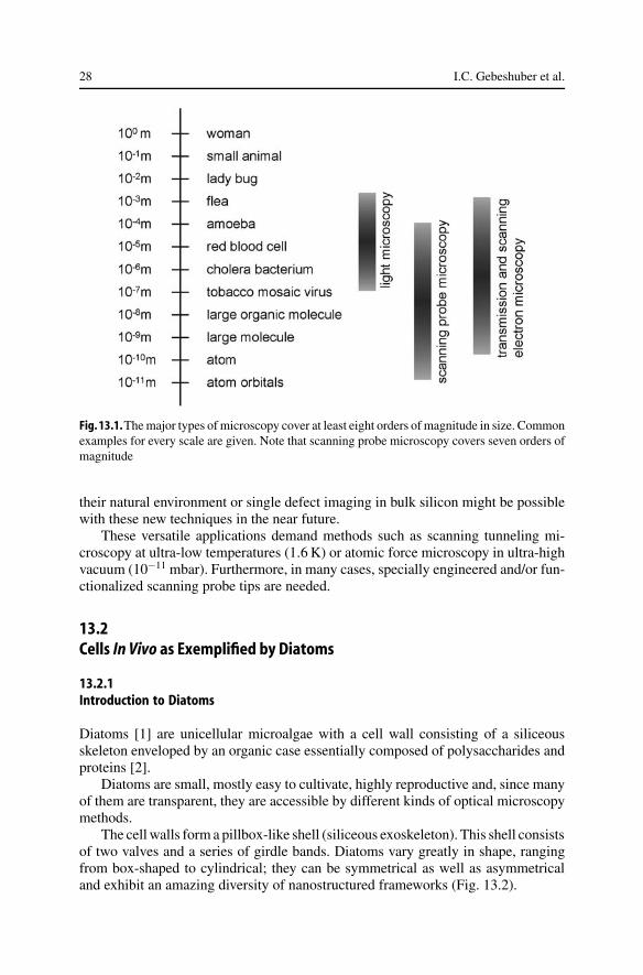
In this chapter the reader will be introduced to scanning probe microscopy of samplesvarying by seven orders of magnitude in size (Fig. 13.1). The largest samples pre-sented are living cells, measuring some hundreds of micrometers. Small units oflife, biomolecules with only some tens of nanometers, are the next sample. They areinvestigated while interacting with each other in real-time. One more step down insize, small ion-induced defects on atomically flat crystals represent structures in thenanometer regime. New data storage devices might result from such investigations.Finally, single electron spin detection (dozens of atomic layers beneath the surface)and the imaging of atom orbitals extend scanning probe microscopy to the subatomicregime. Gathering of 3D atomic-level information of (bio)molecules embedded in
28 I.C. Gebeshuber et al.
Fig. 13.1.The major types of microscopy cover at least eight orders of magnitude in size. Commonexamples for every scale are given. Note that scanning probe microscopy covers seven orders ofmagnitude
their natural environment or single defect imaging in bulk silicon might be possiblewith these new techniques in the near future.
These versatile applications demand methods such as scanning tunneling mi-croscopy at ultra-low temperatures (1.6 K) or atomic force microscopy in ultra-highvacuum (10−11 mbar). Furthermore, in many cases, specially engineered and/or fun-ctionalized scanning probe tips are needed.
13.2Cells In Vivo as Exemplified by Diatoms
13.2.1Introduction to Diatoms
Diatoms [1] are unicellular microalgae with a cell wall consisting of a siliceousskeleton enveloped by an organic case essentially composed of polysaccharides andproteins [2].
Diatoms are small, mostly easy to cultivate, highly reproductive and, since manyof them are transparent, they are accessible by different kinds of optical microscopymethods.
The cell walls form a pillbox-like shell (siliceous exoskeleton). This shell consistsof two valves and a series of girdle bands. Diatoms vary greatly in shape, rangingfrom box-shaped to cylindrical; they can be symmetrical as well as asymmetricaland exhibit an amazing diversity of nanostructured frameworks (Fig. 13.2).

13 Scanning Probe Microscopy: From Living Cells to the Subatomic Range 29
Fig. 13.2. Siliceous exoskeletons of three diatom species imaged with scanning electron micro-scopy. Top: Tricaeratium favus, whole cell (left), detail (right). Bottom: Roperia tessellata (left)and Achnathes brevipes (right). Reprinted with permission from Gebeshuber IC, ThompsonJB, Del Amo Y, Stachelberger H, Kindt JH (2002) Mat Sci Technol 18:763 [4] © 2002 IoMCommunications Ltd.
These naturally nanostructured surfaces gained the attention of nanoscien-tists, and diatom nanotechnology developed as a new interdisciplinary field of re-search [3].
Diatoms are found in freshwater, brackish and marine environments, as well asin moist soils, and on other regularly moist surfaces. They are either freely floating(planktonic forms) or attached to a substratum (benthic forms), and some speciesmay form colonies in the form of chains of cells of varying length. Individual diatomsrange from two micrometers up to several millimeters in size, although only fewspecies are larger than 200 micrometers. Diatoms as a group are very diverse with12,000 to 60,000 species reported [5, 6].
These unicellular organisms are interesting from the point of view of materialsscience and biomimetic studies, since they master challenges as diverse as buildingnanostructured glass-like shells with high load capacity (a problem interesting forlightweight structures architecture) and engineering strong and robust adhesivesthat are stable in wet environments (most man-made adhesives fail to bond inwet conditions, owing to chemical modification of the adhesive or its substrate).Furthermore, diatoms excel at preventing dissolution of their silica shells in waterowing to a covering layer (up-to-date technology is currently facing the problemthat man made glass fiber reinforced polymers show rapid deterioration when usedin water).
Currently, human chemical synthesis cannot produce siliceous structures withthe hierarchical structural detail of the diatom frustules nor can ordered siliceousstructures be produced synthetically under the benign conditions of diatom biomine-
30 I.C. Gebeshuber et al.
ralization. Biosilicification occurs at ambient temperatures and pressures, whereasartificial chemical synthesis of silica-based materials (e.g. resins, molecular sievesand catalysts) requires extreme conditions of temperature, pressure and pH.
13.2.2SPM of Diatoms
The first AFM study of diatoms was presented in 1992 [7]. In this study, the surfacestructure of six different diatom species collected from a mud sample was imagedafter the cells had been briefly rinsed with ethanol to kill, clean and immobilizethem.
Topography and micromechanical properties like elasticity and hardness of deaddiatom cells were reported by Almquist et al. in 2001 [8].
In contrast to these AFM images of dead cells, topography and micromechanicalproperties (such as viscoeleastic properties, adhesion forces and hardness) of thesurface of the living diatom cell has been investigated [e.g. 5, 10–13].
Lee and co-workers combined scanning electrochemical microscopy and scan-ning optical microscopy to obtain simultaneous electrochemical and optical imagesof living diatoms in a constant-current mode [13]. This kind of microscopy mightprove useful in mapping the biochemical activity of a living cell.
The defense potential of the diatom shell was investigated by Hamm and co-workers by measuring its strength [14]. It was found that diatoms are remarkablystrong by virtue of their architecture and the material properties of the diatom silica.
In 2004 Arce and co-workers used the AFM to compare the adhesion of diatomsto several surfaces. Tipless AFM cantilevers were functionalized with living diatomcells, and the surfaces investigated were tested with the same diatom bioprobe [15].
13.2.2.1Diatom Topography as Investigated with AFM
Owing to the poor adhesion to the substrate, it is impossible to obtain stable imagesof most benthic diatom species with the AFM.
AFM-compatible diatom species can be selected from a large sample by fol-lowing a simple and effective strategy: Freshwater aquarium plants covered withbenthic diatoms are placed in a jar filled with water, as well as two left-handedEuropean freshwater snail species, Physa fontinalis and Planorbarius corneus, andsome glass slides. In the following weeks, the diatoms will colonize the jar and theglass slides. The snails will feed on the diatoms, predominantly leaving the speciesbehind, which obviously strongly attach to the substrate.
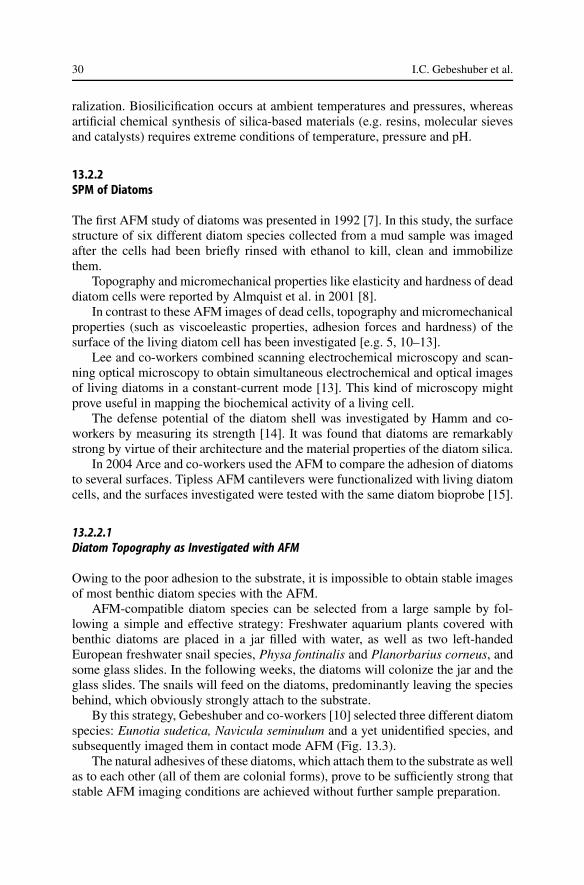
By this strategy, Gebeshuber and co-workers [10] selected three different diatomspecies: Eunotia sudetica, Navicula seminulum and a yet unidentified species, andsubsequently imaged them in contact mode AFM (Fig. 13.3).
The natural adhesives of these diatoms, which attach them to the substrate as wellas to each other (all of them are colonial forms), prove to be sufficiently strong thatstable AFM imaging conditions are achieved without further sample preparation.

13 Scanning Probe Microscopy: From Living Cells to the Subatomic Range 31
Fig. 13.3. AFM image of parts of two living diatom cells of the species Navicula seminulumgrowing on a glass slide. Note that the flat area does not correspond to the surface of the glassslide, but is determined by the maximum possible extension of the z-piezo of the microscope.Image acquired using AFM contact-mode imaging in water, imaging parameter topography,scan size 8 × 8 µm2, scanning frequency 1 Hz. Reprinted with permission from Gebeshuber IC,Kindt JH, Thompson JB, Del Amo Y, Stachelberger H, Brzezinski M, Stucky, GD, Morse DE,Hansma PK (2003) J Microsc 212:292 [10] © 2003, The Royal Microscopical Society
The cells are imaged in their culture medium or in tap water while they are stillgrowing on the glass slides. Tapping-mode as well as contact mode imaging is easyto achieve as long as engaging the cantilever takes place on the cell surface.
Navicula seminulum grows in stacks of cells pointing out from the glass slide.These chains of cells can be about 10 cells high, as investigated by SEM (data notshown). Figure 13.3 reveals detailed surface patterning of the top valve faces of twoadjacent cells of Navicula seminulum.
The chains of Eunotia sudetica and of the yet unidentified species grow withthe valve faces perpendicular to the surface of the glass slide, allowing for AFMinvestigation of the girdle bands.
The cells are alive and continue to divide after imaging.
13.2.2.2Diatom Adhesives Investigated by SPM
Most man-made adhesives fail to bond in wet conditions, owing to chemical modi-fication of the adhesive or its substrate. Engineering strong and robust underwateradhesives that are stable in wet environments is a challenge to current technology.Diatoms produce excellent adhesives that are stable and robust in wet environments.
Phase images depict the phase delay between the drive and response of thecantilever. These images contain information about the energy dissipated during
32 I.C. Gebeshuber et al.
the interaction of the AFM tip with the sample, and can help us to understand theviscoelastic and adhesion properties of the surfaces investigated, specifically of theorganic material responsible for diatom adhesion.
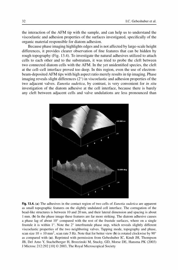
Because phase imaging highlights edges and is not affected by large-scale heightdifferences, it provides clearer observation of fine features that can be hidden byrough topography (Fig. 13.4). To investigate the natural adhesives utilized to attachcells to each other and to the substratum, it was tried to probe the cleft betweentwo connected diatom cells with the AFM. In the yet unidentified species, the cleftat the cell–cell interface proved too deep. In this region, even the use of electron-beam-deposited AFM tips with high aspect ratio merely results in tip imaging. Phaseimaging reveals slight differences (2◦) in viscoelastic and adhesion properties of thetwo adjacent valves. Eunotia sudetica, by contrast, is very convenient for in situinvestigation of the diatom adhesive at the cell interface, because there is barelyany cleft between adjacent cells and valve undulations are less pronounced than
Fig. 13.4. (a) The adhesives in the contact region of two cells of Eunotia sudetica are apparentas small topographic features on the slightly undulated cell interface. The corrugation of thebead-like structures is between 10 and 20 nm, and their lateral dimension and spacing is about1 mm. (b) In the phase image these features are far more striking. The diatom adhesive causesa phase lag of about 10◦ compared with the rest of the frustule surfaces, where on a singlefrustule it is within 1◦. Note the 2◦ interfrustule phase step, which reveals slightly differentviscoelastic properties of the two neighboring valves. Tapping mode, topography and phase,scan size 10 × 10 mm2, scan rate 5 Hz. Note that for better view (b) is rotated clockwise by 90◦
as compared with (a). Reprinted with permission from Gebeshuber IC, Kindt JH, ThompsonJB, Del Amo Y, Stachelberger H, Brzezinski M, Stucky, GD, Morse DE, Hansma PK (2003)J Microsc 212:292 [10] © 2003, The Royal Microscopical Society
13 Scanning Probe Microscopy: From Living Cells to the Subatomic Range 33
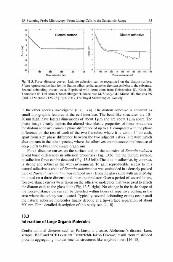
Fig. 13.5. Force–distance curves. Left: no adhesion can be recognized on the diatom surface.Right: representative data for the diatom adhesive that attaches Eunotia sudetica to the substrate.Several debonding events occur. Reprinted with permission from Gebeshuber IC, Kindt JH,Thompson JB, Del Amo Y, Stachelberger H, Brzezinski M, Stucky, GD, Morse DE, Hansma PK(2003) J Microsc 212:292 [10] © 2003, The Royal Microscopical Society
in the other species investigated (Fig. 13.4). The diatom adhesive is apparent assmall topographic features at the cell interface. The bead-like structures are 10–20 nm high, have lateral dimensions of about 1 µm and are about 1 µm apart. Thephase image clearly depicts the altered viscoelastic properties of these structures:the diatom adhesive causes a phase difference of up to 10◦ compared with the phasedifference on the rest of each of the two frustules, where it is within 1◦ on each,apart from a 2◦ phase difference between the two adjacent valves, a feature whichalso appears in the other species, where the adhesives are not accessible because ofdeep clefts between the single organisms.
Force–distance curves on the surface and on the adhesive of Eunotia sudeticareveal basic differences in adhesion properties (Fig. 13.5). On the diatom surface,no adhesion force can be detected (Fig. 13.5 left). The diatom adhesive, by contrast,is strong and robust in the wet environment. To gain reproducible access to thisnatural adhesive, a chain of Eunotia sudetica that was embedded in a densely packedfield of Navicula seminulum was scraped away from the glass slide with an STM-tipmounted on a three-dimensional micromanipulator. Over a period of several hours,force–distance curves were taken on the adhesive molecules that were used to attachthe diatom cells to the glass slide (Fig. 13.5, right). No change in the basic shape ofthe force–distance curves can be detected within hours of repetitive pulling in thearea where the colony was located. Typically, several debonding events occur untilthe natural adhesive molecules finally debond at a tip–surface separation of about600 nm. For a detailed description of this study, see [4, 10].
13.3Interaction of Large Organic Molecules
Conformational diseases such as Parkinson’s disease, Alzheimer’s disease, kuru,scrapie, BSE and vCJD (variant Creutzfeldt-Jakob Disease) result from misfoldedproteins aggregating into detrimental structures like amyloid fibers [16–18].

34 I.C. Gebeshuber et al.
The amount of protein involved ranges from scarcely detectable to kilograms.Partial unfolding might expose significant regions of the polypeptide chain to
the outside world, allowing the protein to aggregate and convert into amyloid fibrils.Once formed, the strong hydrogen bonding between molecules can make this processeffectively irreversible.
As with crystallization, the formation of amyloid fibrils is “seeded” by pre-formed aggregates, a phenomenon that might also be responsible for the rapidprogression of sporadic diseases such as Alzheimer’s once the symptoms becomeevident. BSE, for example, has almost undoubtedly resulted from the highly unnatu-ral practice of feeding young cows on the remains of old ones, with the disease thenbeing transmitted to humans as vCJD. Both kuru and BSE have virtually disappearedas a result of effective action taken once their origins were understood.
The proteins that have emerged under evolutionary pressure are normally robustenough to resist reversion to aggregated states. Evolutionary processes have selectedsequences of amino acids with the remarkable ability to form monomeric structuresin which the main chain is folded in a unique way within the mass of close-packedside chains, preventing it from interacting with other molecules.
Furthermore, “chaperone” proteins help to protect against such changes.Chaperones are proteins whose function is to assist other proteins in achieving
proper folding: They prevent protein aggregation by providing encapsulated hydro-phobic environments that allow the protein to fold properly.
Many chaperones are heat or cold shock proteins, that is, proteins expressed inheat or cold shock conditions. The reason for this behavior is that protein folding isseverely affected by extreme temperatures. Chaperones act to counteract the potentialdamage. Although most proteins can fold in the absence of chaperones, a minoritystrictly requires them.
A large number of chaperones need adenosine triphosphate (ATP) to functionproperly. Chaperones recognize unfolded proteins by the hydrophobic residues theseexpose to the solvent. Exposed hydrophobic residues are unusual for properly foldedproteins. Since the environment of the cell is characterized by hydrophilic groups(mostly water), incompletely folded or misfolded proteins with exposed hydro-phobic groups have a tendency to aggregate to larger structures, where again, thehydrophobic residues would be hidden from the surrounding.
Chaperonins are a subset of chaperone proteins found in prokaryotes, mitochon-dria and plastids.
The AFM has proven to be a useful tool for studying proteins at the singlemolecule level. For a review on single molecule techniques in biomedicine andpharmacology, see [19].
Many of the single molecule studies with the AFM have been restricted by noiseand speed limitations.
The first protein–protein interactions on the single molecule level imaged in realtime were presented in 2000 [20]. This study demonstrated the enormous contribu-tions AFM can make to molecular biology. Bulk results are interesting, but there aremany valuable properties that can only be investigated on the single molecule level.
This work was enabled by the development of small cantilevers [21–23]. Smallcantilevers allow for faster imaging and faster force spectroscopy of single biopo-lymers, because they have higher resonant frequencies and lower coefficients ofviscous damping.
13 Scanning Probe Microscopy: From Living Cells to the Subatomic Range 35
A new generation of AFMs using small cantilevers will enable the study ofbiological processes with greater time resolution, possibly at video refresh rates.Furthermore, small cantilever AFMs allow to narrow the gap in time between resultsfrom force spectroscopy experiments and molecular dynamics calculations.
The small cantilevers are fabricated out of low stress silicon nitride. They areten micrometers long, have widths of 3–5 mm, and their thickness is about 75 nm.These cantilevers can measure smaller forces than larger cantilevers with the samespring constant because they have lower coefficients of viscous damping.
The prototype small AFM detects the motion of small cantilevers by usinghigh numerical aperture optics to focus a laser beam onto the cantilever and thenmeasuring angular changes in the reflected light beam.
This microscopy was used to observe, in real time, the interactions between in-dividual molecules of the Escherichia coli chaperonin protein GroES binding to andthen dissociating from individual E. coli GroEL proteins, which were immobilizedon a mica support.
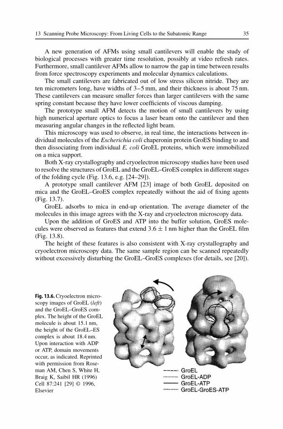
Both X-ray crystallography and cryoelectron microscopy studies have been usedto resolve the structures of GroEL and the GroEL–GroES complex in different stagesof the folding cycle (Fig. 13.6, e.g. [24–29]).
A prototype small cantilever AFM [23] image of both GroEL deposited onmica and the GroEL–GroES complex repeatedly without the aid of fixing agents(Fig. 13.7).
GroEL adsorbs to mica in end-up orientation. The average diameter of themolecules in this image agrees with the X-ray and cryoelectron microscopy data.
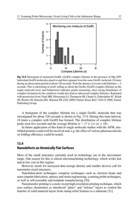
Upon the addition of GroES and ATP into the buffer solution, GroES mole-cules were observed as features that extend 3.6 ± 1 nm higher than the GroEL film(Fig. 13.8).
The height of these features is also consistent with X-ray crystallography andcryoelectron microscopy data. The same sample region can be scanned repeatedlywithout excessively disturbing the GroEL–GroES complexes (for details, see [20]).
Fig. 13.6. Cryoelectron micro-scopy images of GroEL (left)and the GroEL–GroES com-plex. The height of the GroELmolecule is about 15.1 nm,the height of the GroEL–EScomplex is about 18.4 nm.Upon interaction with ADPor ATP, domain movementsoccur, as indicated. Reprintedwith permission from Rose-man AM, Chen S, White H,Braig K, Saibil HR (1996)Cell 87:241 [29] © 1996,Elsevier
36 I.C. Gebeshuber et al.
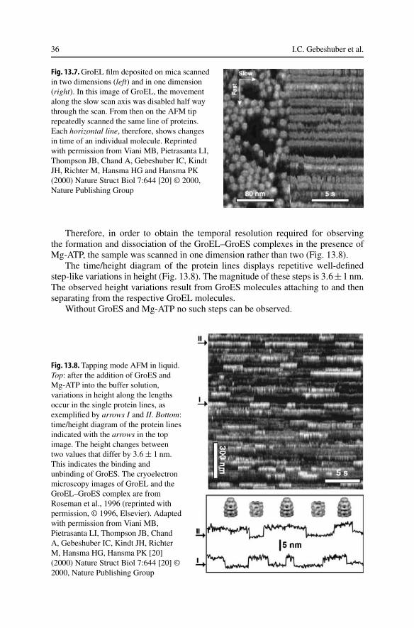
Fig. 13.7. GroEL film deposited on mica scannedin two dimensions (left) and in one dimension(right). In this image of GroEL, the movementalong the slow scan axis was disabled half waythrough the scan. From then on the AFM tiprepeatedly scanned the same line of proteins.Each horizontal line, therefore, shows changesin time of an individual molecule. Reprintedwith permission from Viani MB, Pietrasanta LI,Thompson JB, Chand A, Gebeshuber IC, KindtJH, Richter M, Hansma HG and Hansma PK(2000) Nature Struct Biol 7:644 [20] © 2000,Nature Publishing Group
Therefore, in order to obtain the temporal resolution required for observingthe formation and dissociation of the GroEL–GroES complexes in the presence ofMg-ATP, the sample was scanned in one dimension rather than two (Fig. 13.8).
The time/height diagram of the protein lines displays repetitive well-definedstep-like variations in height (Fig. 13.8). The magnitude of these steps is 3.6±1 nm.The observed height variations result from GroES molecules attaching to and thenseparating from the respective GroEL molecules.
Without GroES and Mg-ATP no such steps can be observed.
Fig. 13.8. Tapping mode AFM in liquid.Top: after the addition of GroES andMg-ATP into the buffer solution,variations in height along the lengthsoccur in the single protein lines, asexemplified by arrows I and II. Bottom:time/height diagram of the protein linesindicated with the arrows in the topimage. The height changes betweentwo values that differ by 3.6 ± 1 nm.This indicates the binding andunbinding of GroES. The cryoelectronmicroscopy images of GroEL and theGroEL–GroES complex are fromRoseman et al., 1996 (reprinted withpermission, © 1996, Elsevier). Adaptedwith permission from Viani MB,Pietrasanta LI, Thompson JB, ChandA, Gebeshuber IC, Kindt JH, RichterM, Hansma HG, Hansma PK [20](2000) Nature Struct Biol 7:644 [20] ©2000, Nature Publishing Group
13 Scanning Probe Microscopy: From Living Cells to the Subatomic Range 37
Fig. 13.9. Histogram of measured GroEL–GroES complex lifetime in the presence of Mg-ATP.Individual GroES molecules attach to and then separate from the same GroEL molecule 18 timesduring an observation period of about 120 seconds. Note the absence of events with lifetimes < 2seconds. This is interesting in itself, telling us about the GroEL-GroES complex lifetime on thesingle molecule level, and furthermore indicates gentle measuring, since strong disturbance ofcomplex formation by the cantilever would also lead to subsecond complex lifetimes. Reprintedwith permission from Viani MB, Pietrasanta LI, Thompson JB, Chand A, Gebeshuber IC, KindtJH, Richter M, Hansma HG, Hansma PK [20] (2000) Nature Struct Biol 7:644 © 2000, NaturePublishing Group
A histogram of the complex lifetime for a single GroEL molecule that wasinvestigated for about 120 seconds is shown in Fig. 13.9. During this time interval,18 times a complex with GroES has formed. The distribution of complex lifetimepeaks near five seconds and the average lifetime is ∼ (7 ± 1) s (n = 18).
In future application of this kind of single molecule studies with the AFM, mis-folded proteins could well be involved and, e.g. the effect of various pharmaceuticalson folding efficiency could be tested.
13.4Nanodefects on Atomically Flat Surfaces
Most of the small structures currently used in technology are in the micrometerrange. One reason for this is silicon micromachining technology, which works fastand at low cost in this regime.
However, needs for increased data-storage density and smaller devices call fornanometer-sized structures.
Nanofabrication techniques comprise techniques such as electron beam andnano-imprint fabrication, epitaxy and strain engineering, scanning probe techniques,as well as self-assembly and template manufacturing [30].
Nanotransfer printing is a more recent high-resolution printing technique, whichuses surface chemistries as interfacial “glues” and “release” layers to control thetransfer of solid material layers from stamp relief features to a substrate [31].
38 I.C. Gebeshuber et al.
One important way to produce nanostructures on surfaces involves kinetic sput-tering by “fast” ions. However, fast ions unavoidably cause unwanted radiationdamage. As opposed to this, potential sputtering (PS), i.e. desorption induced by thepotential energy of slow multiply charged ions (MCI), holds great promise for moregentle nanostructuring of insulating surfaces [32, 33].
It can cause high sputter yields even at such low ion impact energies wherekinetic sputtering and defect creation in deeper layers is not possible. While thephysical mechanisms of PS have been the subject of extensive investigation [34–38],technical applications of slow MCI have so far remained largely unexplored, despitethe fact that they provide unique opportunities for etching, ultra-thin film growthand nanostructure fabrication.
The AFM is the microscope of choice for investigating ion induced nanodefectson flat crystals, because of its unprecedented resolution and of the fact that it canalso image insulating materials.
13.4.1Ion Bombardment of Highly Oriented Pyrolytic Graphite (HOPG)
HOPG is used as a diffracting element in monochromators for X-ray and neutronscattering and as a calibration standard for STM and AFM. The graphite surface iseasily prepared as a clean atomically flat surface by cleavage with an adhesive tape.HOPG is, therefore, used in many laboratories as the surface of choice for “seeingatoms”.
Surface defects in HOPG produced by the impact of individual (singly charged)ions have already been investigated via STM/AFM by a number of groups [40–49,and further references therein].
However, first results were reported only recently for impact of slow multiplycharged ions and the effect of the projectile charge state (or potential energy) on thesize of the produced nanodefects [49–52].
Moreover, in most previous studies, either STM in air was used or the irradiatedsamples were transported in air towards STM inspection after ion bombardment.If, e.g., chemical bonds at the surface are broken due to the ion impact, impuritiescould preferentially adsorb at these sites and thus change the topography of thesurface (and the resulting STM image) during contact with air. Therefore, here MCIbombardment has been followed by STM/AFM investigations without breaking theultra-high vacuum. In this way, possible influences from target surface exposure toair can be ruled out.
Figure 13.10 shows STM and AFM scans of the HOPG surface before bombard-ment.
The STM image of HOPG bombarded with 800 eV Ar+ ions reveals a largenumber of individual nanosized defects as a result of ion bombardment (Fig. 13.11).In AFM scans of the same surface, no significant topographic changes could bedetected [53].
For very highly charged projectile ions, surface defects have recently also beenobserved in AFM studies [51, 52].
Meguro and co-workers found that HCI impact and subsequent treatment eitherby electron injection from an STM tip or by He-Cd laser irradiation induce a localized
13 Scanning Probe Microscopy: From Living Cells to the Subatomic Range 39
Fig. 13.10. Highly oriented pyrolytic graphite imaged in ultrahigh vacuum with atomic resolution.Left: scanning tunneling microscopy image, image size 4×4 nm2. Right: atomic force microscopyimage, image size 1 × 1 nm2
transition from sp2 to sp3 hybridization in graphite, resulting in the formation ofnanoscale diamond-like structures (nanodiamonds) at the impact region [54].
In an investigation of HOPG bombarded with 400 eV Ar+ and Ar8+ ions invol-ving Raman spectroscopy, Hida and co-workers found that the charge state of theions as well as their mass have an influence on the disordering of HOPG and thatthe defects introduced by Ar8+ are not simple vacancies, but assumed to be vacancyclusters in contrast to their results for Ar+ irradiation [55].
Several hundred defects from different sample positions have been statisticallyanalyzed for each projectile type (Ar+, Ar8+, Ar9+).
Fig. 13.11. Highly orien-ted pyrolytic graphitebombarded with 800 eVAr+ ions imaged withSTM in ultrahigh va-cuum. Image size100 × 100 nm2. Theion induced nanodefectsare clearly visible
40 I.C. Gebeshuber et al.
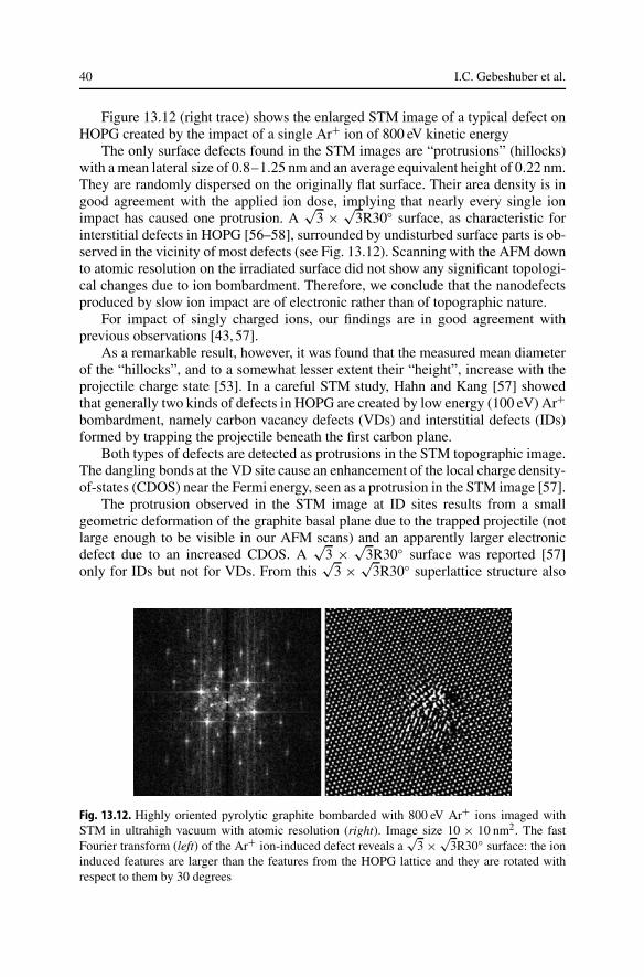
Figure 13.12 (right trace) shows the enlarged STM image of a typical defect onHOPG created by the impact of a single Ar+ ion of 800 eV kinetic energy
The only surface defects found in the STM images are “protrusions” (hillocks)with a mean lateral size of 0.8–1.25 nm and an average equivalent height of 0.22 nm.They are randomly dispersed on the originally flat surface. Their area density is ingood agreement with the applied ion dose, implying that nearly every single ionimpact has caused one protrusion. A
√3 ×
√3R30◦ surface, as characteristic for
interstitial defects in HOPG [56–58], surrounded by undisturbed surface parts is ob-served in the vicinity of most defects (see Fig. 13.12). Scanning with the AFM downto atomic resolution on the irradiated surface did not show any significant topologi-cal changes due to ion bombardment. Therefore, we conclude that the nanodefectsproduced by slow ion impact are of electronic rather than of topographic nature.
For impact of singly charged ions, our findings are in good agreement withprevious observations [43, 57].
As a remarkable result, however, it was found that the measured mean diameterof the “hillocks”, and to a somewhat lesser extent their “height”, increase with theprojectile charge state [53]. In a careful STM study, Hahn and Kang [57] showedthat generally two kinds of defects in HOPG are created by low energy (100 eV) Ar+
bombardment, namely carbon vacancy defects (VDs) and interstitial defects (IDs)formed by trapping the projectile beneath the first carbon plane.
Both types of defects are detected as protrusions in the STM topographic image.The dangling bonds at the VD site cause an enhancement of the local charge density-of-states (CDOS) near the Fermi energy, seen as a protrusion in the STM image [57].
The protrusion observed in the STM image at ID sites results from a smallgeometric deformation of the graphite basal plane due to the trapped projectile (notlarge enough to be visible in our AFM scans) and an apparently larger electronicdefect due to an increased CDOS. A
√3 ×
√3R30◦ surface was reported [57]
only for IDs but not for VDs. From this√
3 ×√
3R30◦ superlattice structure also
Fig. 13.12. Highly oriented pyrolytic graphite bombarded with 800 eV Ar+ ions imaged withSTM in ultrahigh vacuum with atomic resolution (right). Image size 10 × 10 nm2. The fastFourier transform (left) of the Ar+ ion-induced defect reveals a
√3 ×
√3R30◦ surface: the ion
induced features are larger than the features from the HOPG lattice and they are rotated withrespect to them by 30 degrees
13 Scanning Probe Microscopy: From Living Cells to the Subatomic Range 41
observed in our experiments (see Fig. 13.12), we therefore conclude that the majorityof the “hillocks” observed are due to IDs, or VDs created along with IDs. Thestrong increase of the lateral protrusion size with increasing charge state of theprojectile ion is interpreted as a “pre-equilibrium” effect of the stopping of slowmultiply charged ions in HOPG, as has so far only been observed for higher chargestates [44].
Although MCI are converted already into neutral hollow atoms (i.e., an atomwhose inner shells remain essentially unoccupied) during their approach towards thesurface, their captured electrons remain in highly exited states until surface impact,where they are gradually peeled off and replaced by conduction band electronsforming a partial screening cloud around the MCI [59].
Before final deexcitation of the hollow atom can take place within the solid,reduced screening should result in a strongly increased energy loss of the projectiles.According to SRIM-2000 (© IBM) calculations [60], the mean range of 150 eV Arprojectiles in HOPG is about two monolayers. An increased stopping and stragglingof the higher charged Ar projectiles would lead to IDs located closer to the surface,as well as to more VDs due to a higher momentum transfer to the carbon atoms of thefirst plane. Because of the extreme surface sensitivity of STM, this pre-equilibriumeffect in the stopping power is not masked by (equilibrium) bulk effects and isapparently observable with unprecedented clearness.
Extending pertinent work by other groups with singly charged ions only, ourcombined STM/AFM studies revealed nanodefects that comprise a disturbance ofthe electronic density-of-states of the surface rather than its topography.
Whereas the size of these defects increases with the ion charge (here up to q = 9),as expected for any conducting target surface they showed no evidence for potentialsputtering.
For more detailed information on these studies, see [50, 53].
13.4.1.1Revealing the Hidden Atom in Graphite by Low-Temperature AFM
Despite the proverbial ease of imaging graphite by STM with atomic resolution,every second atom in the hexagonal surface unit cell remains hidden, and STMimages show only a single atom in the unit cell.
The reason for this is that the tunneling current is not a function of the surfacetopography, but of the local electronic structure. On the graphite surface, there aretwo different types of carbon atoms in the basal plane, as distinguished by thepresence (α) or absence (β) of a carbon atom in the plane immediately below thesurface. The α atoms are located directly above another α atom, in the layer directlyunderneath, the β atoms are located above a hollow site. These local electronicstructure variations imply that the STM can only detect every other atom on thegraphite surface. Consequently, an alternative imaging method is required to detectthe “hidden” α atoms on the graphite surface [61].
Also in contact-mode AFM images of graphite the quasi-atomic resolutionimages show only one protrusion per unit cell [62].
Recent progress in dynamic AFM allows researchers to routinely achieve trueatomic resolution on conductors and insulators [63, 64], but once again only one
42 I.C. Gebeshuber et al.
maximum within a hexagonal unit cell of the graphite surface was obtained in theattractive noncontact mode [65].
In 2003, Hembacher and co-workers presented measurements with a low-temperature atomic force microscope with pico-Newton force sensitivity that revealthe hidden surface atom [66].
The instrument used in this investigation is a combined ultrahigh vacuum (UHV)STM/AFM to simultaneously probe the charge density at the Fermi level and thetotal charge density of graphite by recording tunneling currents and forces, respec-tively. The instrument is immersed in a liquid He bath cryostat, yielding a sampletemperature of 4.89 K and exceptionally low thermal drifts of about 0.02 nm/h (atroom temperature, even with drift correction, currently 2–10 nm/h are achieved). Toprotect the microscopy from external vibrations, the setup is built on a foundationwith a mass of 30,000 kg.
In their dynamic AFM images of graphite, recorded at small oscillation ampli-tudes and with weak repulsive forces, both the α atoms and the β atoms are detected.The reason for this is that the repulsive forces utilized in AFM involve differentelectrons in the tungsten tip than in the STM mode.
Revealing the hidden atoms in graphite by means of room-temperature AFMmight become possible with miniaturized AFMs based on nano- or microelectro-mechanical systems (NEMS/MEMS) technology (since they show small drift). Insuch an instrument, the operating frequency could be commensurately increased andthere would be no need for a 30,000 kg fundament [61].
13.4.2Bombardment of Single Crystal Insulators with Multicharged Ions
Systematic STM/AFM investigations on nanoscopic defect production at atomicallyclean insulator surfaces of Al2O3 after bombardment by slow (impact energy ≤1.2 keV) singly and multiply charged ions under strict UHV conditions is the topicof this section.
It will be demonstrated that on monocrystalline insulator surfaces, well-definedtopographic features of typically nm extensions are produced (“potential sputte-ring”). For Al2O3, there exists a clear dependence of the defect size on the projectileion charge. These results are discussed in view of possible new nanoscopic surfacestructuring and modification methods for which the kinetic projectile energy playsonly a minor role.
Impact of slow ions on solid surfaces can give rise to inelastic processes thatmodify the geometric and electronic structure at and below the surface, cause emis-sion of electrons and photons as well as neutral and ionized target particles (atoms,molecules, clusters), remove surface-adsorbed material and lead to projectile neu-tralization. The transfer of electrons between surface and projectile possibly acts asprecursor for the above-mentioned processes and makes them proceed irrespectiveof the kinetic projectile energy.
The importance of such “electronic” processes increases with multicharged pro-jectile ions and their role is elucidated when slow ions of the same kinetic energy,but with different charge states are applied as projectiles.
13 Scanning Probe Microscopy: From Living Cells to the Subatomic Range 43
For certain insulator surfaces, the impact of slow multicharged ions (MCIs)Zq+ gives rise to considerably stronger ablation than the well-established kineticsputtering by neutral or ionized projectiles. First experimental evidence for this PSwas reported for alkali-halide surfaces and explained by “Coulomb explosion” [67],i.e. the creation of small positively charged surface spots from the rapid electroncapture by impinging MCI, and the subsequent ablation because of strong mutualtarget ion repulsion.
“Coulomb explosion” was also invoked in order to explain AFM observations ofblister-like defects on mica samples produced by highly charged ions Zq+ (kineticenergy 1–3 keV/atomic mass unit) [36, 68].
However, studies for impact of slow (≤ 1 keV) MCI on thin polycrystallinefilms of alkali-halides (LiF, NaCl) and Al2O3 deposited on quartz microbalancecrystals [69] suggested a different explanation for PS, namely defect-stimulateddesorption induced by very efficient electron capture [35].
It has been established that such desorption processes are induced by electrons(electron stimulated desorption, ESD) or photons (photon stimulated desorption,PSD) on such materials where self-trapping of specific crystal defects proceeds viaelectron–phonon coupling in the crystal lattice [70].
However, such defect trapping as the prerequisite for PS may also be caused orat least supported by the kinetic projectile energy (“kinetically assisted PS” [37]),which could also explain some PS-like effects reported for target species whereno electron–phonon coupling can take place, i.e. for semiconductors like Si andGaAs [68]. In any case, for slow ion impact, the self-trapping mechanism is mostrelevant for PS. Consequently, for metal and semiconductor surfaces no slow MCI-induced PS can be observed, so far [71].
As the surface region from which a slow MCI does capture electrons should berather small (nm extensions), it is probable that the surface defects caused by PS areof similar size. In order to study such defect structures, we applied AFM in UHVon monocrystalline target surfaces of insulator species for which PS by slow MCIimpact has already been demonstrated on polycrystalline thin films [37, 69, 71].
The results for Al2O3 presented below are of possible interest for nanostructuringthese surfaces.
Observations of slow ion-induced nanodefects on different atomically cleantarget surfaces were performed under strict UHV conditions with a combinedAFM/STM instrument (UHV-AFM/STM, OMICRON Nanotechnology GmbH, Ger-many). Nanodefects were looked for on freshly prepared surfaces of sapphire c-planeAl2O3(0001) after irradiation with low doses of slow singly and multiply chargedions. In order to avoid disturbing noise from an ion irradiation chamber directlyattached to the AFM/STM instrument, a transportable UHV vault for target transfer,which was alternatingly coupled via UHV locks to the target ion irradiation chamberand the AFM/STM was used. This procedure kept the target surfaces under perma-nent UHV conditions after initial cleaning, thermal annealing, and during subsequentslow ion irradiation until completion of the AFM/STM inspection. Ion irradiation ofthe insulator surfaces was accompanied by low-energy (≤ 4 eV) electron floodingto compensate for surface charge-up, which otherwise strongly inhibits AFM obser-vation or makes it even impossible. The electron gun was arranged at 2 cm distance

44 I.C. Gebeshuber et al.
to the sample. All AFM observations were made in the contact mode, with the basepressure in the AFM/STM chamber kept at about 10−10 mbar during measurements.
The singly and multiply charged ions for target irradiation have been extractedfrom a 5 GHz electron cyclotron resonance ion source [72], magnetically analyzedand guided via electrostatic lenses to the UHV irradiation chamber. The ions weredecelerated in front of the target surface to their desired impact energy (≤ 1.2 keV).Uniform irradiation was assured by rapidly scanning the ion beam across the targetsurface by means of deflection plates.
13.4.2.1Production of Slow Ion-Induced Surface Defects on Al2O3 Insulator Targets
Polished Al2O3(0001) c-plane single crystals (TBL Kelpin, Neuhausen, Germany)were CO2 snow cleaned (to remove micrometer and submicrometer particles andhydrocarbon-based contamination) and then annealed in UHV for 3 h at 400 ◦C. Thispreparation technique yields very flat crystal surfaces.
AFM contact mode studies on 14 samples prepared by the standard preparationtechnique revealed a root mean square (rms) roughness of 0.093 ± 0.06 nm rms.Bombardment with Ar ions of different charge states and kinetic energies (500 eVAr+ and Ar7+, 1.2 keV Ar+, Ar4+ and Ar7+) results – as seen in AFM contact mode– in hillock-like nanodefects (see Fig. 13.13).
The ion-induced defects on the sapphire single crystal surface can be removed byannealing at 450 ◦C for 5 h. The density of nanodefects does not directly correspondwith the applied ion dose: an ion dose of 5 × 10¹² ions/cm2, which is equivalent tofive ions per 10 nm × 10 nm, leads to a rather small, however reproducible, densityof defects on the sapphire surface: about 10 nanodefects per 1000 nm×1000 nm canbe observed after bombardment in the energy range reported here. This is equivalent
Fig. 13.13. UHV AFM contact mode image of sapphire (Al2O3, c-plane 0001) bombarded with500 eV Ar+ (left image) and Ar7+ (right image) ions. The nanodefects induced by Ar7+ ions(which have the same kinetic but higher potential energy than the Ar+ ions) are considerablyhigher and wider than those caused by singly charged ions. The defects are real topographicfeatures; the units on the three axes are nanometers. Reprinted with permission from GebeshuberIC, Cernusca S, Aumayr F, Winter HP (2003) Int J Mass Spectrom 229:27 [53] © 2003, ElsevierScience B.V.

13 Scanning Probe Microscopy: From Living Cells to the Subatomic Range 45
to a dose to defect ratio of 5000. More detailed experiments with different ion dosesare needed. Analysis of the statistics of random impacts will clarify how manyindividual ion impacts are needed to form a visible nanodefect on the insulatorsurface.
A possibly similar migration and subsequent recombination of point defects atthe surface has previously been reported for silicon bombarded by 5 keV He ionsabove 160 K [73].
In fact, the only case where the number of defects corresponded fairly well tothe applied ion dose was for the conducting HOPG samples (see Sect. 13.4.1).
The Al2O3 c-plane proved to be the insulator surface showing most clearlya dependence of the ion bombardment induced defects with the kinetic energy andcharge states of the projectiles. 500 eV Ar+ ions produce defects that are about1 nm high (Fig. 13.13) and have lateral dimensions of some tens of nanometers(one should keep in mind that the height is more accurately measurable with theAFM than lateral dimensions), whereas the defects produced by 500 eV Ar7+ ionsare several nanometers high (Fig. 13.13) and show lateral dimensions of about 100(!) nanometers. At higher kinetic energy the differences in the slow ion-inducednanodefects on the sapphire c-plane became even more distinct.
1.2 keV Ar+-induced defects are up to about 8 nm high and their width is some10 nm. For a higher charge state such as Ar4+, two different kinds of defects occurredon the sapphire surface.
They have about the same height, but their lateral dimensions vary considerably:some are nearly 200 nm wide, whereas the smaller defects are only about 50 nmwide.
The height of both kinds of defects is about 2 nm. For Ar7+, only one kind ofdefect was visible in the AFM images, with about 50 nm diameter and about 2 nmheight (for a more detailed description of these results and for similar investigationon SiO2 surfaces, see [53]).
Al2O3 is, therefore, a good candidate for PS-induced nanostructuring. This ma-terial is relevant for applications in microelectronics and nanotechnology.
13.5Subatomic Features
In this section, the detection of atomic orbitals and single electron spins by means ofSPM is described. In many cases, sophisticated signal acquisition techniques haveto be applied, and the instruments have to be operated at very low temperature, sinceextremely small drift is required.
13.5.1Atom Orbitals
Silicon and tungsten are the two chemical elements that already have been investi-gated with SPM regarding their atomic orbitals.

46 I.C. Gebeshuber et al.
13.5.1.1Silicon (111)-(7 × 7) Surface
Publications concerning the imaging of subatomic features with the AFM startedin the year 2000, when Giessibl and co-workers published their paper on imagingof subatomic features on the reconstructed silicon (111)-(7 × 7) surface [74]. Fora review on semiconductor surface reconstruction, see [75].
A scientific discussion, in which Hug and co-workers questioned this result byproposing that the subatomic features are caused by a feedback artifact, followedthis publication [76].
In the course of this argument, Giessibl and co-workers presented refined calcu-lations, showing striking similarities to the experimental images (see Fig. 13.14).
In 2003, Huang and co-workers presented a theoretical work demonstrating thefeasibility of seeing atomic orbitals on the Si(111)-(7 × 7) surface with AFM [77].
Fig. 13.14. Refined calculations of the normalized frequency shift of a single adatom on thereconstructed silicon (111)-(7 × 7) surface (right) performed by the Giessibl group, showingstriking similarities with the experimental images (left). Reprinted with permission from Hug HJ,Lantz MA, Abdurixit A, van Schendel PJA, Hoffmann R, Kappenberger P, Baratoff A, GiessiblFJ, Hembacher S, Bielefeldt H, Mannhart J (2001) Science 291:2509 [76] © 2001, AAAS
13.5.1.2Tungsten
In 2004, Giessibl and co-workers finally ended this discussion by presenting imagesof an individual tungsten atom by AFM at a resolution of 77 pm [78]. The diameter ofa tungsten atom is 274 pm. Four distinct peaks that are attributed to highly localizedelectron clouds can be identified (Fig. 13.15).
The experiment was performed in UHV at a temperature of about five Kelvin.The microscope was isolated from vibrations by a 30 t foundation and from soundand electromagnetic stray fields by a metal chamber.
In contrast to STM (which only probes the most loosely bound electrons withenergies at the Fermi level) AFM can resolve the charge density variations withina single atom, because the forces between the AFM tip and the sample are ofelectrostatic nature.

13 Scanning Probe Microscopy: From Living Cells to the Subatomic Range 47
Fig. 13.15. UHV low temperature (5 K) AFMconstant-height mode image reveals four-fold symmetryin the amplitudes of the higher harmonics signal(centered close to the maximum of the tunneling current,data not shown). Reprinted with permission fromHembacher S, Giessibl FJ and Mannhart J (2004) Science305:380 [78] © 2004, AAAS
The electron structure originates from the quantum-mechanical nature of tungs-ten bonding: tungsten develops a body centered cubic crystal structure such thatevery tungsten atom is surrounded by eight nearest neighbor atoms, causing “arms”of increased charge density which point to the next neighbors. Four of these preciselylocalized electron clouds are visible on surface atoms.
The role of tip and sample was switched in the experiment: the front atom ina sharp tungsten tip was imaged by a light carbon atom of a graphite surface. Thereason a light atom was used for probing was to minimize image blurring, sincethe mapping of one atom with another atom always involves a convolution of theelectronic states. The tunneling current is confined to the top atom because of thesharp increase of tunneling probability with decreasing distance.
Instead of measuring static deflections or frequency changes, higher harmonicstriggered by forces between the tip and the sample are recorded in this technique.These higher harmonics are much more sensitive to short-range interactions thanstatic deflections or frequency changes.
13.5.2Single Electron Spin Detection with AFM and STM
Single-spin detection is a vital goal for read-out in quantum computing, and singlenuclear spin detection could solve the problem of how to distinguish between mate-rials at the atomic level.
Several research groups have reported various single spin-detection methods[79–86].
In 1989, Manassen and co-workers presented the first direct observation ofthe precession of individual paramagnetic spins on partially oxidized silicon (111)surfaces [79].
They used an STM to detect the modulation in the tunneling current at the Larmorfrequency. The Larmor frequency is the frequency at which magnetic resonancecan be excited. It is given by the Larmor equation, which states that the resonantfrequency is proportional to the overall (macroscopic and microscopic) magneticfield. Balatsky and Martin presented the theoretical explanation of this result [87] in2001.
48 I.C. Gebeshuber et al.
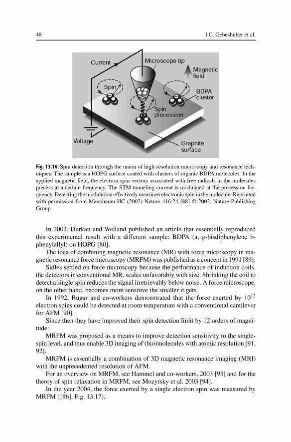
Fig. 13.16. Spin detection through the union of high-resolution microscopy and resonance tech-niques. The sample is a HOPG surface coated with clusters of organic BDPA molecules. In theapplied magnetic field, the electron-spin vectors associated with free radicals in the moleculesprecess at a certain frequency. The STM tunneling current is modulated at the precession fre-quency. Detecting the modulation effectively measures electronic spin in the molecule. Reprintedwith permission from Manoharan HC (2002) Nature 416:24 [88] © 2002, Nature PublishingGroup
In 2002, Durkan and Welland published an article that essentially reproducedthis experimental result with a different sample: BDPA (a, g-bisdiphenylene b-phenylallyl) on HOPG [80].
The idea of combining magnetic resonance (MR) with force microscopy in ma-gnetic resonance force microscopy (MRFM) was published as a concept in 1991 [89].
Sidles settled on force microscopy because the performance of induction coils,the detectors in conventional MR, scales unfavorably with size. Shrinking the coil todetect a single spin reduces the signal irretrievably below noise. A force microscope,on the other hand, becomes more sensitive the smaller it gets.
In 1992, Rugar and co-workers demonstrated that the force exerted by 1012
electron spins could be detected at room temperature with a conventional cantileverfor AFM [90].
Since then they have improved their spin detection limit by 12 orders of magni-tude:
MRFM was proposed as a means to improve detection sensitivity to the single-spin level, and thus enable 3D imaging of (bio)molecules with atomic resolution [91,92].
MRFM is essentially a combination of 3D magnetic resonance imaging (MRI)with the unprecedented resolution of AFM.
For an overview on MRFM, see Hammel and co-workers, 2003 [93] and for thetheory of spin relaxation in MRFM, see Mozyrsky et al. 2003 [94].
In the year 2004, the force exerted by a single electron spin was measured byMRFM ([86], Fig. 13.17).
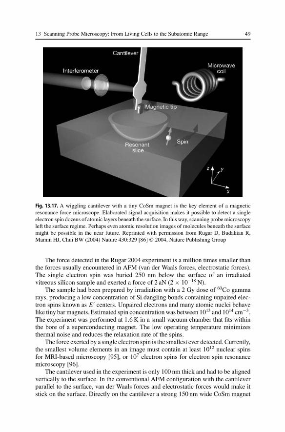
13 Scanning Probe Microscopy: From Living Cells to the Subatomic Range 49
Fig. 13.17. A wiggling cantilever with a tiny CoSm magnet is the key element of a magneticresonance force microscope. Elaborated signal acquisition makes it possible to detect a singleelectron spin dozens of atomic layers beneath the surface. In this way, scanning probe microscopyleft the surface regime. Perhaps even atomic resolution images of molecules beneath the surfacemight be possible in the near future. Reprinted with permission from Rugar D, Budakian R,Mamin HJ, Chui BW (2004) Nature 430:329 [86] © 2004, Nature Publishing Group
The force detected in the Rugar 2004 experiment is a million times smaller thanthe forces usually encountered in AFM (van der Waals forces, electrostatic forces).The single electron spin was buried 250 nm below the surface of an irradiatedvitreous silicon sample and exerted a force of 2 aN (2 × 10⁻¹⁸ N).
The sample had been prepared by irradiation with a 2 Gy dose of 60Co gammarays, producing a low concentration of Si dangling bonds containing unpaired elec-tron spins known as E ′ centers. Unpaired electrons and many atomic nuclei behavelike tiny bar magnets. Estimated spin concentration was between 1013 and 1014 cm−3.The experiment was performed at 1.6 K in a small vacuum chamber that fits withinthe bore of a superconducting magnet. The low operating temperature minimizesthermal noise and reduces the relaxation rate of the spins.
The force exerted by a single electron spin is the smallest ever detected. Currently,the smallest volume elements in an image must contain at least 1012 nuclear spinsfor MRI-based microscopy [95], or 107 electron spins for electron spin resonancemicroscopy [96].
The cantilever used in the experiment is only 100 nm thick and had to be alignedvertically to the surface. In the conventional AFM configuration with the cantileverparallel to the surface, van der Waals forces and electrostatic forces would make itstick on the surface. Directly on the cantilever a strong 150 nm wide CoSm magnet

50 I.C. Gebeshuber et al.
is attached. It generates a field gradient of 200,000 T/m. The cantilever is slowlyscanned over the surface. A laser interferometer records the cantilever deflections andsophisticated measurement signal acquisition techniques are needed for successfulsingle spin detection. The strong magnetic field gradient allows for distinguishingmagnetic resonance signals arising from different spatial locations, enabling accuratespin localization. By scanning the tip over the sample, a local magnetic resonanceforce is detected, which corresponds with a spatial resolution of about 25 nm. Thisspatial isolation of the signal is also the main argument that a single spin is beingdetected. Currently this method is very slow. As Stokstad mentions in his “ScienceNews of the Week” article on the Rugar experiment, scanning a 170 nm stretch ofthe irradiated silicon sample took several weeks [97].
MRFM could serve as an invaluable tool for the implementation of a spin-based solid state quantum computer. It provides an attractive means for addressingthe characterization and control of the fabrication process of the device during itsconstruction and the readout of the computational result [98, 99].
If developed further, the MRFM technique could prove useful for investigatingthe atomic structure inside materials used in the electronics industry and to imagebiomolecules – such as proteins – at atomic resolution. However, to reach this goal,nuclear spins have to be detected. Nuclear spins are harder to detect than electronspins, because a proton’s magnetic moment is 658 times smaller than that of anelectron.
13.6Conclusions and Outlook
In this review, we have presented scanning probe microscopy across dimensionsfrom large samples like single cells, via single biomolecules and nanometer smallion induced defects on crystal surfaces to subatomic features like electronic orbitalsand single electron spins.
Scanning probe microscopy is on its way to a standard laboratory method:subatomic features can be imaged, and with magnetic resonance force microscopyit has even left the two-dimensional surface regime. Perhaps in the not too distantfuture 3D-imaging of (complex) molecules, at surfaces or in the bulk state, withatomic resolution might become possible with these powerful techniques. The 3-DMRFM would also deliver chemical specific information because each magneticnucleus has a unique gyromagnetic ratio.
Acknowledgements. Part of this work was supported by the Austrian Science Fund (FWF) andwas carried out at Vienna University of Technology.
Part of this work was funded by the “Austrian Kplus-Program” and was done at the “AustrianCenter of Competence for Tribology”, AC2T research GmbH.

13 Scanning Probe Microscopy: From Living Cells to the Subatomic Range 51
References
1. Round FE, Crawford RM, Mann DG (1990) Diatoms: biology and morphology of thegenera, Cambridge University Press
2. Hecky RE, Mopper K, Kilham P, Degens ET (1973) Marine Biol 19:3233. Gordon R, Sterrenburg F, Sandhage K (guest eds) (2005) Diatom nanotechnology, special
issue J Nanosci Nanotechnol 5:14. Gebeshuber IC, Thompson JB, Del Amo Y, Stachelberger H, Kindt JH (2002) Mat Sci
Technol 18:7635. Werner D (1977) The biology of diatoms, University of California Press6. Gordon R, Drum RW (1994) Int Rev Cytol 150:2437. Linder A, Colchero J, Apell H-J, Marti O, Mlynek J (1992) Ultramicrosc 42-44:3298. Almqvist N, Delamo Y, Smith BL, Thomson NH, Bartholdson A, Lal R, Brzezinski M,
Hansma PK (2001) J Microsc 202:5189. Higgins MJ, Crawford SA, Mulvaney P, Wetherbee R (2002) Protist 153:25
10. Gebeshuber IC, Kindt JH, Thompson JB, Del Amo Y, Stachelberger H, Brzezinski M,Stucky GD, Morse DE, Hansma PK (2003a) J Microsc 212:292
11. Higgins MJ, Sader JE, Mulvaney P, Wetherbee R (2003a) J Phycol 39:72212. Higgins MJ, Molino P, Mulvaney P, Wetherbee R (2003b) J Phycol 39:118113. Lee Y, Ding Z, Bard AJ (2002) Anal Chem 74:363414. Hamm CE, Merkel R, Springer O, Jurkojc P, Maier C, Prechtel K, Smetacek V (2003)
Nature 421:84115. Arce FT, Avci R, Beech IB, Cooksey KE, Wigglesworth-Cooksey B (2004) Biophys J
87(6):428416. Solomon B, Taraboulos A, Katchalski-Katzir E (2002) Conformational diseases: a com-
pendium based on the 1st international workshop on conformational diseases, S KargerPub, Tunbridge Wells, UK
17. Dobson CM (2002) Nature 418:72918. Dobson CM (2003) Nature 426:88419. Greulic KO (2004) Curr Pharmac Biotech 5:24320. Viani MB, Pietrasanta LI, Thompson JB, Chand A, Gebeshuber IC, Kindt JH, Richter M,
Hansma HG, Hansma PK (2000) Nature Struct Biol 7:64421. Walters DA, Cleveland JP, Thomson NH, Hansma PK, Wendman MA, Gurley G, Elings
V (1996) Rev Sci Instrum 67:358322. Viani MB, Schäffer TE, Chand A, Rief M, Gaub HE, Hansma PK (1999a) J Appl Phys
86:225823. Viani MB, Schäffer TE, Paloczi GT, Pietrasanta LI, Smith BL, Thompson JB, Richter M,
Rief M, Gaub HE, Plaxco KW, Cleland AN, Hansma HG, Hansma PK (1999b) Rev SciInstrum 70:4300
24. Braig K, Otwinowski Z, Hegde R, Boisvert DC, Joachimiak A, Horwich AL, Sigler PB(1994) Nature 371:578
25. Hunt JF, Weaver AJ, Landry SJ, Gierasch L, Eisenhofer J (1996) Nature 379:3726. Boisvert DC, Wang J, Otiwonowski Z, Horwich AL, Sigler PB (1996) Nature Struct Biol
3:17027. Xu Z, Horwich AL, Sigler PB (1997) Nature 388:74128. Chen S, Roseman AM, Hunter AS, Wood SP, Burston SG, Ranson NA, Clarke AR, Saibil
HR (1994) Nature 371:26129. Roseman AM, Chen S, White H, Braig K, Saibil HR (1996) Cell 87:24130. Ziaie B, Baldi A, Atashbar MZ (2004) Introduction to micro/nanofabrication In: Bhushan
B (ed) Springer handbook of nanotechnology. Springer, Berlin Heidelberg New York,p 147
52 I.C. Gebeshuber et al.
31. Rogers JA (2004) Stamping techniques for micro and nanofabrication: methods and ap-plications. In: Bhushan B (ed) Springer handbook of nanotechnology. Springer, BerlinHeidelberg New York, p 185
32. Arnau A, Aumayr F, Echenique PM, Grether M, Heiland W, Limburg J, Morgenstern R,Roncin P, Schippers S, Schuch R, Stolterfoht N, Varga P, Zouros TJM, Winter HP (1997)Surf Sci Rep 27:113
33. Winter HP, Aumayr F (2002) Europhys News 6:21534. Sporn M, Libiseller G, Neidhart T, Schmid M, Aumayr F, Winter HP, Varga P, Grether M,
Niemann D, Stolterfoht N (1997) Phys Rev Lett 79:94535. Aumayr F, Burgdörfer J, Varga P, Winter HP (1999) Comm Atom Molecul Phys 34:20136. Schenkel T, Hamza AV, Barnes AV, DH Schneider (1999) Progr Surf Sci 61:2337. Hayderer G, Cernusca S, Schmid M, Varga P, Winter HP, Aumayr F, Niemann D, Hoffmann
V, Stolterfoht N, Lemell C, Wirtz L, Burgdörfer J (2001) Phys Rev Lett 86:353038. Hayderer G, Schmid M, Varga P, Winter HP, Aumayr F, Wirtz L, Lemell C, Burgdörfer J,
Hägg L, Reinhold CO (1999) Phys Rev Lett 83:394839. Porte L, de Villeneuve CH, Phaner M (1991) J Vac Sci Technol B 9, 106440. Coregater R, Claverie A, Chahboun A, Landry V, Ajustron F, Beauvillain J (1992) Surf
Sci 262:20841. You HX, Brown NMD, Al-Assadi KF (1992) Surf Sci 279:18942. Mazukawa T, Suzuki S, Fukai T, Tanaka T and Ohdomari I (1996) Appl Surf Sci 107:22743. Mochiji K, Yamamoto S, Shimizu H, Ohtani S, Seguchi T, Kobayashi N (1997) J Appl
Phys 82:603744. Reimann KP, Bolse W, Geyer U, Lieb KP (1995) Europhys Lett 30:46345. Habenicht S, Bolse W, Feldermann H, Geyer U, Hofsäss H, Lieb KP, Roccaforte F (2000)
Europhys Lett 50:20946. Neumann R (1999) Nucl Instrum Meth B 151:4247. Hahn R, Kang K, Song S, J Jeon (1996) Phys Rev B 53:172548. Hahn R, Kang K (1999) Phys Rev B 60:60049. Minniti R, Ratliff LP, Gillaspy JD (2001) Phys Scr T92:2250. Hayderer G, Cernusca S, Schmid M, Varga P, Winter HP, Aumayr F (2001) Phys Scr
T92:15651. Terada M, Nakamura N, Nakai Y, Kanai Y, Ohtani S, Komaki K, Yamazaki Y (2004)
Observation of an HCI-induced nano-dot on an HOPG surface with STM and AFM In:Rudzikas Z (ed) Abstracts HCI-2004 12th international conference on the physics of highlycharged ions, European Physical Society, p 208
52. Terada M, Nakamura N, Nakai Y, Kanai Y, Ohtani S, Komaki K, Yamazaki Y (2005) NuclInstrum Meth Phys Res B 235:452
53. Gebeshuber IC, Cernusca S, Aumayr F and Winter HP (2003) Int J Mass Spectrom 229:2754. Meguro T, Hida A, Koguchi Y, Miyamoto S, Yamamoto Y, Takai H, Maeda K, Aoyagi Y
(2003) Nuc Instrum Meth B 209:17055. Hida A, Meguro T, Maeda K, Aoyagi Y (2003) Nuc Instrum Meth B 205:73656. Hahn R, Kang K, Song S, Jeon J (1996) Phys Rev B 53:172557. Hahn R, Kang K (1999) Phys Rev B 60:600758. Krasheninnikov AV, Elsin F (2000) Surf Sci 519:45459. Winter HP, Aumayr F (1999) J Phys B: At Mol Opt Phys 32: R3960. Ziegler JF, Biersack JP, Littmark U (1985) The stopping and range of ions in matter 1.
Pergamon, New York61. Hersam MC and Chung Y-W (2003) Proc Natl Acad Sci 100:1253162. Albrecht TR and Quate CF (1988) J Vac Sci Technol A 6:27163. Morita S, Wiesendanger R, Meyer E (2002) (eds) Noncontact atomic force microscopy.
Springer, New York
13 Scanning Probe Microscopy: From Living Cells to the Subatomic Range 53
64. Giessibl FJ (2003) Rev Mod Phys 75:94965. Hölscher H, Allers W, Schwarz UD, Schwarz A, Wiesendanger R (2000) Phys Rev B
62:696766. Hembacher S, Giessibl FJ, Mannhart J, Quate CF (2003) Proc Nat Acad Sci 100:1253967. Bitensky IS, Murakhmetov MN, Parilis ES (1979) Sov Phys Tech Phys 25:61868. Schneider DH, Briere MA, McDonald J, Biersack J (1993) Radiat Eff Def Sol 127:11369. Hayderer G, Schmid M, Varga P, Winter HP, Aumayr F (1999) Rev Sci Instrum 70:369670. Townsend P (1983) In: Behrisch R (ed) Sputtering by particle bombardment II. Berlin,
Heidelberg, New York, p 14771. Varga P, Neidhard T, Sporn M, Libiseller G, Schmid M, Aumayr F, Winter HP (1997) Phys
Scr T73:30772. Leitner M, Wutte D, Brandstötter J, Aumayr F, Winter HP (1994) Rev Sci Instrum 65:109173. Bedrossian PJ, de la Rubia TD (1998) J Vac Sci Technol A 16:104374. Giessibl FJ, Hembacher S, Bielefeldt H, Mannhart J (2000) Science 289:42275. Duke CB (1996) Chem Rev 96:123776. Hug HJ, Lantz MA, Abdurixit A, van Schendel PJA, Hoffmann R, Kappenberger P, Baratoff
A, Giessibl FJ, Hembacher S, Bielefeldt H, Mannhart J (2001) Science 291:250977. Huang M, Cuma M, Liu F (2003) Phys Rev Lett 90:25610178. Hembacher S, Giessibl FJ, Mannhart J (2004) Science 305:38079. Manassen Y, Hamers RJ, Demuth JE, Castellano AJ jun (1989) Phys Rev Lett 62:253180. Durkan C, Welland ME (2002) Appl Phys Lett 80:45881. Wrachtrup J, von Borczyskowski C, Bernard J, Orritt M, Brown R (1993) Nature 363:24482. Köhler J, Disselhorst JAJM, Donckers MCJM, Groenen EJJ, Schmidt J, Moerner WE
(1993) Nature 363:24283. Jelezko F, Popa I, Gruber A, Tietz C, Wrachtrup J, Nizovtsev A, Kilin S (2002) Appl Phys
Lett 81:216084. Elzerman JM, Hanson R, Willems van Beveren LH, Witkamp B, Vandersypen LMK,
Kouwenhoven LP (2004) Nature 430:43185. Xiao M, Martin I, Yablonovitch E, Jiang HW (2004) Nature 430:43586. Rugar D, Budakian R, Mamin HJ, Chui BW (2004) Nature 430:32987. Balatsky AV, Martin I (2002) Quant Inf Proc 1:35588. Manoharan HC (2002) Nature 416:2489. Sidles JA (1991) Appl Phys Lett 58:285490. Rugar D, Yannoni CS, Sidles JA (1992) Nature 360:56391. Sidles JA (1992) Phys Rev Lett 68:112492. Sidles JA, Garbini JL, Bruland KJ, Rugar D, Züger O, Hoen S, Yannoni CS (1995) Rev
Mod Phys 67:24993. Hammel PC, Pelekhov DV, Wigen PE, Gosnell TR, Midzor MM, Roukes ML (2003) Proc
IEEE 91:78994. Mozyrsky D, Martina I, Pelekhov D, PC Hammel (2003) Appl Phys Lett 82:127895. Ciobanu L, Seeber DA, Pennington CH (2002) J Magn Reson 158:17896. Blank A, Dunnam CR, Borbat PP, Freed JH (2003) J Magn Reson 165:1197. Stokstad E (2004) Science 305:32298. Berman GP, Doolen GD, Hammel PC, Tsifrinovich VI (2000) Phys Rev B 61:1469499. Pelekhov DV, Martin I, Suter A, Reagor, DW, Hammel PC (2002) Proc SPIE 4656:1
![THE COW - Institut für Angewandte Physik [IAP/TU Wien]gebeshuber/Nanotechnology_of_the_cow_VetLife... · Production Rohan Lingam Photographer Craig Biggs Contributor Arvind Raj Selva](https://static.documents.pub/doc/80x56/5e1d1b3ae161f12bce24af0b/the-cow-institut-fr-angewandte-physik-iaptu-wien-gebeshubernanotechnologyofthecowvetlife.jpg)


