33
Sitara™ AM335x ARM ® Cortex™-A8 Microprocessors (MPUs) Silicon Revisions 2.1, 2.0, 1.0 Silicon Errata Literature Number: SPRZ360E October 2011–Revised April 2013

Sitara™ AM335x ARM® Cortex™-A8Microprocessors (MPUs)Silicon Revisions 2.1, 2.0, 1.0
Silicon Errata
Literature Number: SPRZ360E
October 2011–Revised April 2013

Contents
1 Introduction ........................................................................................................................ 31.1 AM335x Device and Development Support Tool Nomenclature .................................................. 3
1.2 Revision Identification ................................................................................................... 4
2 All Errata Listed With Silicon Revision Number ...................................................................... 63 Usage Notes and Known Design Exceptions to Functional Specifications ................................. 8
3.1 Usage Notes ............................................................................................................. 83.1.1 LCD: Color Assignments of LCD_DATA Terminals ..................................................... 83.1.2 DDR3: JEDEC Compliance for Maximum Self-Refresh Command Limit ............................ 83.1.3 Boot: USB Boot ROM Code Uses Default DATAPOLARITY .......................................... 93.1.4 Boot: Multiplexed Signals GPMC_WAIT0, GMII2_CRS, and RMII2_CRS_DV Cause NAND Boot
Issue ........................................................................................................... 93.1.5 Pin Multiplexing: Valid IO Sets and Restrictions ....................................................... 103.1.6 Boot: Multiplexed Signals GPMC_WAIT0 and GMII2_CRS Cause NAND Boot Issue ........... 103.1.7 OSC1: RTC_XTALIN Terminal Has an Internal Pull-up Resistor When OSC1 is Disabled ...... 11
3.2 Known Design Exceptions to Functional Specifications .......................................................... 12
Revision History ......................................................................................................................... 32
2 Table of Contents SPRZ360E–October 2011–Revised April 2013Submit Documentation Feedback
Copyright © 2011–2013, Texas Instruments Incorporated

Silicon ErrataSPRZ360E–October 2011–Revised April 2013
Sitara™ AM335x ARM® Cortex™-A8Microprocessors (MPUs)
(Silicon Revision 2.1, 2.0, 1.0)
1 Introduction
This document describes the known exceptions to the functional specifications for the Sitara™ AM335xARM® Cortex™-A8 Microprocessors (MPUs). [See the Sitara AM335x ARM Cortex-A8 Microprocessors(MPUs) data manual (literature number SPRS717).]
For additional information, see the latest version of the Sitara AM335x ARM Cortex-A8 Microprocessors(MPUs) Technical Reference Manual (literature number SPRUH73).
1.1 AM335x Device and Development Support Tool Nomenclature
To designate the stages in the product development cycle, TI assigns prefixes to the part numbers of allmicroprocessors (MPUs) and support tools. Each device has one of three prefixes: X, P, or null (no prefix)(for example, XAM3358ZCE). Texas Instruments recommends two of three possible prefix designators forits support tools: TMDX and TMDS. These prefixes represent evolutionary stages of product developmentfrom engineering prototypes (TMDX) through fully qualified production devices and tools (TMDS).
Device development evolutionary flow:
X — Experimental device that is not necessarily representative of the final device's electricalspecifications and may not use production assembly flow.
P — Prototype device that is not necessarily the final silicon die and may not necessarily meet finalelectrical specifications.
null — Production version of the silicon die that is fully qualified.
Support tool development evolutionary flow:
TMDX — Development-support product that has not yet completed Texas Instruments internalqualification testing.
TMDS — Fully-qualified development-support product.
X and P devices and TMDX development-support tools are shipped against the following disclaimer:
"Developmental product is intended for internal evaluation purposes."
Production devices and TMDS development-support tools have been characterized fully, and the qualityand reliability of the device have been demonstrated fully. TI's standard warranty applies.
Predictions show that prototype devices (X or P) have a greater failure rate than the standard productiondevices. Texas Instruments recommends that these devices not be used in any production systembecause their expected end-use failure rate still is undefined. Only qualified production devices are to beused.
Sitara is a trademark of Texas Instruments.Cortex is a trademark of ARM Ltd or its subsidiaries.ARM is a registered trademark of ARM Ltd or its subsidiaries.All other trademarks are the property of their respective owners.
3SPRZ360E–October 2011–Revised April 2013 Sitara™ AM335x ARM® Cortex™-A8 Microprocessors (MPUs) (SiliconRevision 2.1, 2.0, 1.0)Submit Documentation Feedback
Copyright © 2011–2013, Texas Instruments Incorporated

Lot Trace Code
XAM3352AZCE
YMLLLLS
962 ZCE
G1
Device Revision Lot Trace Code
XAM3359AZCZ
YMLLLLS
962 ZCZ
G1
Device Revision
Introduction www.ti.com
1.2 Revision Identification
The device revision can be determined by the symbols marked on the top of the package. Figure 1provides an example of the AM335x device markings.
Figure 1. Example of Device Revision Codes for the AM335x Microprocessor
NOTES:(A) Non-qualified devices are marked with the letters "X" or "P" at the beginning of the device name, while
qualified devices have a "blank" at the beginning of the device name.
(B) The AM3352 and AM3359 devices shown in this device marking example are two of several valid partnumbers for the AM335x family of devices.
(C) The device revision code is the device revision (A, B, and so on).
(D) YM denotes year and month.
(E) LLLL denotes Lot Trace Code.
(F) 962 is a generic family marking ID.
(G) G1 denotes green, lead-free.
(H) ZCE or ZCZ is the package designator.
(I) S denotes Assembly Site Code.
(J) On some "X" devices, the device speed may not be shown.
4 SPRZ360E–October 2011–Revised April 2013Sitara™ AM335x ARM® Cortex™-A8 Microprocessors (MPUs) (SiliconRevision 2.1, 2.0, 1.0) Submit Documentation Feedback
Copyright © 2011–2013, Texas Instruments Incorporated

www.ti.com Introduction
Silicon revision is identified by a code marked on the package. The code is of the format AM3352x orAM3358x, where "x" denotes the silicon revision. Table 1 lists the information associated with each siliconrevision for each device type. For more details on device nomenclature, see the device-specific datamanual.
Table 1. Production Device Revision Codes
DEVICE REVISION CODE SILICON REVISION COMMENTS
(blank) 1.0 Silicon revision is new
A 2.0 Silicon revision 2.0
B 2.1 Silicon revision 2.1
Each silicon revision uses a specific revision of TI's ARM® Cortex™-A8 processor. The ARM Cortex-A8processor variant and revision can be read from the Main ID Register. The DEVREV field (bits 31-28) ofthe Device_ID register located at address 0x44E10600 provides a 4-bit binary value that represents thedevice revision. The ROM code revision can be read from address 2BFFCh. The ROM code versionconsists of two decimal numbers: major and minor. The major number is always 22, minor number countsROM code version. The ROM code version is coded as hexadecimal readable values; for example, ROMversion 22.02 is coded as 0000 2202h. Table 2 shows the ARM Cortex-A8 Variant and Revision, DeviceRevision, and ROM Code Revision values for each silicon revision of the device.
Table 2. Silicon Revision Variables
SILICON ARM CORTEX-A8 DEVICE ROMREVISION VARIANT AND REVISION REVISION REVISION
1.0 r3p2 0000 22.02
2.0 r3p2 0001 22.03
2.1 r3p2 0010 22.03
5SPRZ360E–October 2011–Revised April 2013 Sitara™ AM335x ARM® Cortex™-A8 Microprocessors (MPUs) (SiliconRevision 2.1, 2.0, 1.0)Submit Documentation Feedback
Copyright © 2011–2013, Texas Instruments Incorporated

All Errata Listed With Silicon Revision Number www.ti.com
2 All Errata Listed With Silicon Revision Number
Advisories are numbered in the order in which they were added to this document. Some advisory numbersmay be moved to the next revision and others may have been removed because the design exceptionwas fixed or documented in the device-specific data manual or peripheral user's guide. When items aremoved or deleted, the remaining numbers remain the same and are not re-sequenced.
Table 3. All Usage Notes
SILICON REVISION AFFECTEDNUMBER TITLE
1.0 2.0 2.1
Section 3.1.1 LCD: Color Assignments of LCD_DATA Terminals X X X
DDR3: JEDEC Compliance for Maximum Self-RefreshSection 3.1.2 X X XCommand Limit
Section 3.1.3 Boot: USB Boot ROM Code Uses Default DATAPOLARITY X X X
Boot: Multiplexed Signals GPMC_WAIT0, GMII2_CRS, andSection 3.1.4 XRMII2_CRS_DV Cause NAND Boot Issue
Section 3.1.5 Pin Multiplexing: Valid IO Sets and Restrictions X X X
Boot: Multiplexed Signals GPMC_WAIT0 and GMII2_CRSSection 3.1.6 X XCause NAND Boot Issue
OSC1: RTC_XTALIN Terminal Has an Internal Pull-upSection 3.1.7 X X XResistor When OSC1 is Disabled
Table 4. All Design Exceptions to Functional Specifications
SILICON REVISION AFFECTEDNUMBER TITLE
1.0 2.0 2.1
DDR2, DDR3, mDDR PHY: Control and Status RegistersAdvisory 1.0.1 X X XConfigured for Write Only
Debug Subsystem: EMU[4:2] Signals Are Not Available byAdvisory 1.0.2 X X XDefault After Reset
Debug Subsystem: Internal Inputs Tied-off to the WrongAdvisory 1.0.3 X X XValue
Advisory 1.0.4 PRU-ICSS: Clock Domain Crossing (CDC) Issue X
Advisory 1.0.5 RTC: 32.768-kHZ Clock is Gating Off X
EXTINTn: Input Function of the EXTINTn Terminal isAdvisory 1.0.6 XInverted
Advisory 1.0.7 Boot: Ethernet Boot ROM Code PHY Link Speed Detection X
Boot: Ethernet Boot ROM Code Sends an Incorrect VendorAdvisory 1.0.8 XClass Identifier in BOOTP Packet
Ethernet Media Access Controller and Switch Subsystem:Advisory 1.0.9 C0_TX_PEND and C0_RX_PEND Interrupts Not Connected X
to ARM Cortex-A8
GMII_SEL Register: RGMII1_IDMODE andAdvisory 1.0.10 RGMII2_IDMODE Bits Reset to Non-supported Mode of X
Operation
USB: Attached Non-compliant USB Device that RespondsAdvisory 1.0.11 Xto Spurious Invalid Short Packet May Lock Up Bus
UART: Extra Assertion of FIFO Transmit DMA Request,Advisory 1.0.12 X X XUARTi_DMA_TX
USB: Data May be Lost When USB Subsystem is OperatingAdvisory 1.0.13 in DMA Mode and More Than One Endpoint is Transferring X
Data
GMII_SEL and CPSW Related Pad Control Registers:Advisory 1.0.14 Context of These Registers is Lost During Transitions of X
PD_PER
ARM Cortex-A8: OPP50 Operation on MPU Domain NotAdvisory 1.0.15 XSupported
6 SPRZ360E–October 2011–Revised April 2013Sitara™ AM335x ARM® Cortex™-A8 Microprocessors (MPUs) (Silicon Revision2.1, 2.0, 1.0) Submit Documentation Feedback
Copyright © 2011–2013, Texas Instruments Incorporated

www.ti.com All Errata Listed With Silicon Revision Number
Table 4. All Design Exceptions to Functional Specifications (continued)
SILICON REVISION AFFECTEDNUMBER TITLE
1.0 2.0 2.1
RMII: 50-MHz RMII Reference Clock Output Does NotAdvisory 1.0.16 X X XSatisfy Clock Input Requirements of RMII Ethernet PHYs
Advisory 1.0.17 VDDS_DDR: High-Power Consumption During DeepSleep0 X
ROM: Ethernet Boot Code Does Not Change DefaultAdvisory 1.0.18 Direction of RMII1 Reference Clock When Booting from X
Ethernet Using RMII
DDR3: Fully-Automated Hardware READ and WRITEAdvisory 1.0.19 X X XLeveling Not Supported
Boot: USB Boot ROM Code Overlapping Data in TXFIFOAdvisory 1.0.20 Xand RXFIFO
SmartReflex: Limited Support Due to Issue Described inAdvisory 1.0.21 XAdvisory 1.0.15
EMIF: Dynamic Voltage Frequency Scaling (DVFS) is NotAdvisory 1.0.22 X X XSupported
Ethernet Media Access Controller and Switch Subsystem:Advisory 1.0.23 X X XReset Isolation Feature is Not Supported
Boot: System Boot is Not Reliable if Reset is AssertedAdvisory 1.0.24 X X XWhile Operating in OPP50
Boot: System Boot Temporarily Stalls if an Attempt to BootAdvisory 1.0.25 X X Xfrom Ethernet is Not Successful
Advisory 1.0.26 I2C: SDA and SCL Open-Drain Output Buffer Issue X X
Advisory 1.0.27 LCDC: LIDD DMA Mode Issue X X X
LCDC: Raster Mode, Hardware Auto Underflow RestartAdvisory 1.0.28 X X XDoes Not Work
Latch-up Performance: Latch-up Performance Limits forAdvisory 1.0.29 X XSilicon Revsions 1.0 and 2.0
7SPRZ360E–October 2011–Revised April 2013 Sitara™ AM335x ARM® Cortex™-A8 Microprocessors (MPUs) (SiliconRevision 2.1, 2.0, 1.0)Submit Documentation Feedback
Copyright © 2011–2013, Texas Instruments Incorporated

23 22 21 20 19 18 17 16 15 14 13 12 11 10 9 8 7 6 5 4 3 2 1 0
PIXEL_n
0 0 0 0 0 0 0 0 R[7:3] G[7:2] B[7:3]
16-bit panel
24-bit panel
23 22 21 20 19 18 17 16 15 14 13 12 11 10 9 8 7 6 5 4 3 2 1 0
PIXEL_n
B[0] G[0] R[0] B[1] G[1] R[1] B[2] R[2] B[7:3] G[7:2] R[7:3]
16-bit panel
24-bit panel
Usage Notes and Known Design Exceptions to Functional Specifications www.ti.com
3 Usage Notes and Known Design Exceptions to Functional Specifications
3.1 Usage Notes
This document contains Usage Notes. Usage Notes highlight and describe particular situations where thedevice's behavior may not match presumed or documented behavior. This may include behaviors thataffect device performance or functional correctness. These notes may be incorporated into futuredocumentation updates for the device (such as the device-specific data manual), and the behaviors theydescribe may or may not be altered in future device revisions.
3.1.1 LCD: Color Assignments of LCD_DATA Terminals
The blue and red color assignments to the LCD data pins are reversed when operating in RGB888(24bpp) mode compared to RGB565 (16bpp) mode. In order to correctly display RGB888 data from theSGX, or any source formatted as RGB in memory, it is necessary to connect the LCD panel as shown inFigure 2. Using the LCD Controller with this connection scheme limits the use of RGB565 mode. Any datagenerated for the RGB565 mode requires the red and blue color data values be swapped in order todisplay the correct color.
Figure 2. RGB888 Mode LCD Controller Output Pin Mapping (LCD_DATA[23:0])
When operating the LCD Controller in RGB565 mode the LCD panel should be connected as shown inFigure 3. Using the LCD Controller with this connection scheme limits the use of RGB888 mode. Any datagenerated for the RGB888 mode requires the red and blue color data values be swapped in order todisplay the correct color.
Figure 3. RGB565 Mode LCD Controller Output Pin Mapping (LCD_DATA[23:0])
3.1.2 DDR3: JEDEC Compliance for Maximum Self-Refresh Command Limit
When using DDR3 EMIF Self-Refresh, it is possible to violate the maximum refresh command requirementspecified in the JEDEC standard DDR3 SDRAM Specification (JESD79-3E, July 2010). This requirementstates that the DDR3 EMIF controller should issue no more than 16 refresh commands within any 15.6-μsinterval.
To avoid this requirement violation, when using the DDR3 EMIF and Self-Refresh (setting LP_MODE =0x2 field in the PMCR), the SR_TIM value in the PMCR must to be programmed to a value greater than orequal to 0x9.
8 SPRZ360E–October 2011–Revised April 2013Sitara™ AM335x ARM® Cortex™-A8 Microprocessors (MPUs) (SiliconRevision 2.1, 2.0, 1.0) Submit Documentation Feedback
Copyright © 2011–2013, Texas Instruments Incorporated

www.ti.com Usage Notes and Known Design Exceptions to Functional Specifications
3.1.3 Boot: USB Boot ROM Code Uses Default DATAPOLARITY
The AM335x USB PHYs supports a DATAPOLARITY feature that allows the data plus (DP) and dataminus (DM) data signals to be swapped. This feature was added to simplify PCB layout.
In some cases, the DP and DM data signals may need to cross over each other to connect to therespective USB connector pins. Crossing these signals on the PCB may cause signal integrity issues if notimplemented properly since they must be routed as high-speed differential transmission lines. TheDATAPOLARITY feature in the USB PHYs can be used resolve this issue.
The DATAPOLARITY feature is controlled by DATAPOLARITY_INV (bit 23) of the respective USB_CTRLregister.
The USB boot ROM code uses the default value for DATAPOLARITY_INV when booting from USB.Therefore, the PCB must be designed to use the default DATAPOLARITY if the system must support USBboot.
3.1.4 Boot: Multiplexed Signals GPMC_WAIT0, GMII2_CRS, and RMII2_CRS_DV Cause NAND BootIssue
The AM335x device multiplexes the GPMC_WAIT0, GMII2_CRS, and RMII2_CRS_DV signals on thesame terminal. This causes a problem when the system must support NAND boot while an MII or RMIIEthernet PHY is connected to port 2 of the Ethernet media access controller and switch (CPSW). TheGPMC_WAIT0 signal is required for NAND boot. The GMII2_CRS or RMII2_CRS_DV signal is required bythe respective MII or RMII Ethernet PHY and the only pin multiplexing option for these signals isGPMC_WAIT0.
In this case, there are two sources that need to be connected to the GPMC_WAIT0 terminal. The NANDREADY or BUSY output must source the GPMC_WAIT0 terminal during NAND boot and the MII CRS orRMII CRS_DV output must source the GPMC_WAIT0 terminal when the application software is using port2 of the CPSW. Therefore, a GPIO-controlled external 2-to-1 multiplexer must be implemented in thesystem to select between the two sources. The GPIO selected to control the 2-to-1 multiplexer needs tohave an internal or external resistor that selects the NAND READY or BUSY output as soon as power isapplied and remains in that state until the application software initializes the CPSW.
The TI TS5A3157 SPDT analog switch is an example device that can be used as a 2-to-1 multiplexer.This device inserts minimum propagation delay to the signal path since it is an analog switch. Thepropagation delay inserted by the 2-to-1 multiplexer must be analyzed to confirm it does not cause timingviolations for the respective interface.
The NAND, Ethernet PHY, AM335x VDDSHV1, AM335x VDDSHV3 (when using the ZCZ package), and2-to-1 multiplexer IO power supply domains may need to operate at the same voltage since they sharecommon signals.
9SPRZ360E–October 2011–Revised April 2013 Sitara™ AM335x ARM® Cortex™-A8 Microprocessors (MPUs) (SiliconRevision 2.1, 2.0, 1.0)Submit Documentation Feedback
Copyright © 2011–2013, Texas Instruments Incorporated

Usage Notes and Known Design Exceptions to Functional Specifications www.ti.com
3.1.5 Pin Multiplexing: Valid IO Sets and Restrictions
The AM335x device contains many peripheral interfaces. In order to reduce package size and loweroverall system cost while maintaining maximum functionality, many of the AM335x terminals can multiplexup to eight signal functions. Although there are many combinations of pin multiplexing that are possible,only a certain number of sets, called IO Sets, are valid due to timing limitations. These valid IO Sets werecarefully chosen to provide many possible application scenarios for the user.
Texas Instruments has developed a Windows®-based application called Pin Mux Utility that helps asystem designer select the appropriate pin-multiplexing configuration for their AM335x-based productdesign. The Pin Mux Utility provides a way to select valid IO Sets of specific peripheral interfaces toensure the pin multiplexing configuration selected for a design only uses valid IO Sets supported by theAM335x device.
A few IO Sets have additional restrictions not defined in the Pin Mux Utility. These additional restrictionsare described below:
• MMC0, MMC1, MMC2 Interfaces
– Only Standard (STD) and High Speed (HS) modes are supported. SDR12, SDR25, SDR50 modesas defined in SD3.0 specification are not supported.
• GEMAC_CPSW Interface
– Operation of GEMAC_CPSW is not supported for OPP50.
3.1.6 Boot: Multiplexed Signals GPMC_WAIT0 and GMII2_CRS Cause NAND Boot Issue
The AM335x device multiplexes the GPMC_WAIT0 and GMII2_CRS signals on the same terminal. Thiscauses a problem when the system must support NAND boot while an MII Ethernet PHY is connected toport 2 of the Ethernet media access controller and switch (CPSW). The GPMC_WAIT0 signal is requiredfor NAND boot. The GMII2_CRS signal is required by the MII Ethernet PHY and the only pin multiplexingoption for these signals is GPMC_WAIT0.
In this case, there are two sources that need to be connected to the GPMC_WAIT0 terminal. The NANDREADY or BUSY output must source the GPMC_WAIT0 terminal during NAND boot and the MII CRSoutput must source the GPMC_WAIT0 terminal when the application software is using port 2 of theCPSW. Therefore, a GPIO-controlled external 2-to-1 multiplexer must be implemented in the system toselect between the two sources. The GPIO selected to control the 2-to-1 multiplexer needs to have aninternal or external resistor that selects the NAND READY or BUSY output as soon as power is appliedand remains in that state until the application software initializes the CPSW.
The TI TS5A3157 SPDT analog switch is an example device that can be used as a 2-to-1 multiplexer.This device inserts minimum propagation delay to the signal path since it is an analog switch. Thepropagation delay inserted by the 2-to-1 multiplexer must be analyzed to confirm it does not cause timingviolations for the respective interface.
The NAND, Ethernet PHY, AM335x VDDSHV1, AM335x VDDSHV3 (when using the ZCZ package), and2-to-1 multiplexer IO power supply domains may need to operate at the same voltage since they sharecommon signals.
10 SPRZ360E–October 2011–Revised April 2013Sitara™ AM335x ARM® Cortex™-A8 Microprocessors (MPUs) (SiliconRevision 2.1, 2.0, 1.0) Submit Documentation Feedback
Copyright © 2011–2013, Texas Instruments Incorporated

www.ti.com Usage Notes and Known Design Exceptions to Functional Specifications
3.1.7 OSC1: RTC_XTALIN Terminal Has an Internal Pull-up Resistor When OSC1 is Disabled
The RTC_XTALIN terminal has an internal pull-up resistor that is turned on when OSC1 is disabled. OSC1is disabled by default after power is applied.
This internal pull-up resistor was not properly documented in data sheet revisions D and earlier. Theseearly data sheet revisions recommended an external pull-down resistor to be connected to theRTC_XTALIN terminal if OSC1 was not used. The recommendation should have been to leave thisterminal open-circuit when not using OSC1.
Connecting an external pull-down to the RTC_XTALIN terminal may cause unexpected leakage current.
The current recommendation is to remove any external pull-down resistor from the RTC_XTALIN terminaland leave this terminal open-circuit when not using OSC1.
11SPRZ360E–October 2011–Revised April 2013 Sitara™ AM335x ARM® Cortex™-A8 Microprocessors (MPUs) (SiliconRevision 2.1, 2.0, 1.0)Submit Documentation Feedback
Copyright © 2011–2013, Texas Instruments Incorporated

Usage Notes and Known Design Exceptions to Functional Specifications www.ti.com
3.2 Known Design Exceptions to Functional Specifications
The following advisories are known design exceptions to functional specifications. Advisories arenumbered in the order in which they were added to this document. Some advisory numbers may bemoved to the next revision and others may have been removed because the design exception was fixedor documented in the device-specific data manual or peripheral user's guide. When items are moved ordeleted, the remaining numbers remain the same and are not re-sequenced.
Advisory 1.0.1 DDR2, DDR3, mDDR PHY: Control and Status Registers Configured for Write Only
Revisions Affected 2.1, 2.0, 1.0
Details The DDR2, DDR3, mDDR PHY control and status registers mapped in address range0x44e12000-0x44E123FF are configured for write-only operations, so the contents ofthese register cannot be read.
These registers must be configured by performing write-only operations.
Workarounds There is no workaround for this issue.
Advisory 1.0.2 Debug Subsystem: EMU[4:2] Signals Are Not Available by Default After Reset
Revisions Affected 2.1, 2.0, 1.0
Details All Debug subsystem components should remain unchanged when warm reset isasserted. For example, warm reset should not affect export of debug trace messages onthe EMU[4:0] signals.
The AM335x EMU[4:2] signals can not be used to export trace messages from theDebug subsystem since AM335x does support warm reset and the EMU[4:2] signals arenot assigned to pins after reset is asserted.
Workarounds Do not assert warm reset while performing trace functions.
Advisory 1.0.3 Debug Subsystem: Internal Inputs Tied-off to the Wrong Value
Revisions Affected 2.1, 2.0, 1.0
Details Internal inputs dbg_dpio_attr_dp_app_owner[4:0] and dbg_dpio_attr_dp_debug_only[4:0]to the Debug subsystem are used to report which EMU[4:0] signals can currently beused to export trace messages. These inputs were tied-off to the wrong value. The tie-offvalues used always indicates EMU[4:2] signals are not available and EMU[1:0] signalsare available to export trace messages.
This should not cause a problem for EMU[4:2] since these signals can not be used toexport trace messages for the reason explained in advisory 1.3. However, the AM335xpins used for EMU[1:0] signals may be configured as GPIO. The Debug subsystemwould not know these signals are not available for exporting trace messages when thesepins are configured as GPIO.
Workarounds Do not configure the AM335x EMU[1:0] pins to operate as GPIO if you need to exporttrace messages.
12 SPRZ360E–October 2011–Revised April 2013Sitara™ AM335x ARM® Cortex™-A8 Microprocessors (MPUs) (SiliconRevision 2.1, 2.0, 1.0) Submit Documentation Feedback
Copyright © 2011–2013, Texas Instruments Incorporated

www.ti.com Usage Notes and Known Design Exceptions to Functional Specifications
Advisory 1.0.4 PRU-ICSS: Clock Domain Crossing (CDC) Issue
Revisions Affected 1.0
Details The PRU-ICSS has a clock domain crossing issue when the MII receive multiplexer isconfigured to connect PR1_MII1 signals to PRU0 and PR1_MII0 signals to PRU1.
The multiplexer logic always uses the PR1_MII_MR0_CLK input to synchronize thePRU0 MII receive signals and the PR1_MII_MR1_CLK input to synchronize the PRU1MII receive signals. This cause the wrong clock to be used when the MII receivemultiplexer is configured to connect PR1_MII1 signals to PRU0 and PR1_MII0 signals toPRU1.
As a result of this issue, support for EtherCAT media redundancy is not available.
Workarounds There is no workaround for this issue.
Advisory 1.0.5 RTC: 32.768-kHZ Clock is Gating Off
Revisions Affected 1.0
Details The RTC has a clock gating issue that stops the internal 32.768-kHz clock when theVDD_CORE voltage domain drops below the recommended operating range or thePWRONRSTn input terminal is held low. This issue has the following side effects:
• The RTC counters stop incrementing when the 32.768-kHz clock is gated. Thiscauses the RTC to lose time while the clock is gated.
• A wakeup event applied to the EXT_WAKEUP input terminal is masked if theEXT_WAKEUP_DB_EN bit in the RTC PMIC register (0x98) is set to 1 which enablesthe de-bounce function for the EXT_WAKEUP input. This occurs because the32.768-kHz clock is being used to clock the de-bounce circuit.
Workarounds Do not turn off the VDD_CORE power source or source a logic low to the PWRONRSTninput while expecting RTC to keep an accurate time.
Do not enable the de-bounce circuit on the EXT_WAKEUP input if an external wakeupevent needs to be detected while the 32.768-kHz clock is gated.
Advisory 1.0.6 EXTINTn: Input Function of the EXTINTn Terminal is Inverted
Revisions Affected 1.0
Details The EXTINTn input is active high.
Workarounds Use an active high interrupt source or use an external inverter to change the polarity ofany active low interrupt source.
13SPRZ360E–October 2011–Revised April 2013 Sitara™ AM335x ARM® Cortex™-A8 Microprocessors (MPUs) (SiliconRevision 2.1, 2.0, 1.0)Submit Documentation Feedback
Copyright © 2011–2013, Texas Instruments Incorporated

Usage Notes and Known Design Exceptions to Functional Specifications www.ti.com
Advisory 1.0.7 Boot: Ethernet Boot ROM Code PHY Link Speed Detection
Revisions Affected 1.0
Details The device ROM code relies on the external PHY's Control Register (Register 0),specifically bits 0.6 [Speed Selection (MSB)] and 0.13 [Speed Selection (LSB)], todetermine the operating speed of the link.
If the external PHY does not update its link speed selection bits to reflect the currentoperating speed, the ROM code incorrectly assumes the PHY is operating at the speedindicated by the link speed selection bits and configure the device Ethernet MAC to thewrong speed. For example, if the default value of the PHY link speed selection bitsindicates 100 Mbps, when the PHY is actually operating at 1 Gbps, the ROM incorrectlyconfigures the device Ethernet MAC for 100 Mbps mode.
The IEEE 802.3 specification states: When the Auto-Negotiation Enable (bit 0.12) isenabled, bits 0.6 and 0.13 can be read or written to, but the state of bits 0.6 and 0.13have no effect on the link configuration, and it is not necessary for bits 0.6 and 0.13 toreflect the operating speed of the link when it is read. While some PHYs update the linkspeed in these bits to reflect the current operating speed, other PHYs do not updatethese bits because it is not mandatory according to the specification.
Workarounds When using Ethernet boot, an external PHY that updates the Register 0 link speedselection bits (0.6 and 0.13) to reflect the current operating speed is required.
Advisory 1.0.8 Boot: Ethernet Boot ROM Code Sends an Incorrect Vendor Class Identifier inBOOTP Packet
Revisions Affected: 1.0
Details: When using Ethernet boot, the device ROM code should send a BOOTP request with aunique identifier to distinguish itself from other devices on the same network. Instead,the ROM code sends the same identifier, "DM814x ROM v1.0", for all devices (DM814x,DM816x, and AM335x); hence, the download host attempting to bootstrap the devicescan no longer determine which device is requesting the code to be downloaded.
Applications using the DM814x, DM816x, and AM335x devices cannot coexist in thesame network if they are booted from Ethernet.
Workaround: There is no workaround for this issue.
For some applications, it might be necessary to uniquely identify and service BOOTPpackets from a client. The recommended approach to uniquely identify clients is to usethe MAC address. Every device comes with a unique MAC address. A list of MACaddresses and the device type can be made available to the host in advance, so that thehost can take device-specific action when it receives a BOOTP packet from a MACaddress on the host's list.
14 SPRZ360E–October 2011–Revised April 2013Sitara™ AM335x ARM® Cortex™-A8 Microprocessors (MPUs) (SiliconRevision 2.1, 2.0, 1.0) Submit Documentation Feedback
Copyright © 2011–2013, Texas Instruments Incorporated

www.ti.com Usage Notes and Known Design Exceptions to Functional Specifications
Advisory 1.0.9 Ethernet Media Access Controller and Switch Subsystem: C0_TX_PEND andC0_RX_PEND Interrupts Not Connected to ARM Cortex-A8
Revisions Affected 1.0
Details The Ethernet Media Access Controller/Switch (CPSW) subsystem C0_TX_PEND andC0_RX_PEND interrupt outputs provide a single transmit interrupt that combinestransmit channel interrupts TXPEND[7:0] and a single receive interrupt that combinesreceive channel interrupts RXPEND[7:0]. The TXPEND[0] and RXPEND[0] interruptoutputs are connected to the ARM Cortex-A8 interrupt controller (INTC) rather than theC0_TX_PEND and C0_RX_PEND interrupt outputs. This only allows channel 0 tointerrupt the ARM Cortex-A8.
The C0_TX_PEND and C0_RX_PEND interrupt outputs are the only interrupt outputsthat support interrupt pacing. If transmit channel interrupts 1-7, receive channel interrupts1-7, or interrupt pacing is required, the following workaround must be implemented.
Workarounds DMTIMER Workaround
The C0_TX_PEND and C0_RX_PEND interrupts can be re-routed to the ARM Cortex-A8through two of the AM335x timers. TIMER5 and TIMER6 can be used when configuredto operate in capture mode. The time captured while operating in this mode is notrelevant, since the capture event notification to the ARM Cortex-A8 represents theoriginal causal interrupts coming from the EMAC and Switch subsystem.
The re-routed interrupts path are:
• ARM Cortex-A8: TINT5 (interrupt 93) <-- TIMER5 Capture Event <-- [Event CaptureMux: event 8] <-- EMAC and Switch: C0_RX_PEND
• ARM Cortex-A8: TINT6 (interrupt 94) <-- TIMER6 Capture Event <-- [Event CaptureMux: event 9] <-- EMAC and Switch: C0_TX_PEND
Configuration
The following configurations are required to use timer capture module interrupts:
• TIMER5 and TIMER6 are enabled with capture mode during initialization.
– Set bit 2 of the TIMER5 IRQENABLE set register located at 0x4804_602C to 1b.
– Set bit 2 of the TIMER6 IRQENABLE set register located at 0x4804_802C to 1b.
• Write the value 0x908 to the TIMER_EVT_CAPT register located at 0x44E1_0FD0 toselect EMAC and Switch event 8 (C0_RX_PEND) for TIMER 5 and EMAC andSwitch event 9 (C0_TX_PEND) for TIMER6.
• Configure TIMER5 and TIMER6 to single-capture mode by resetting theCAPT_MODE bit of each TCLR register.
– Reset bit 13 of the TIMER5 TCLR register located at 0x4804_6038 to 0b.
– Reset bit 13 of the TIMER6 TCLR register located at 0x4804_8038 to 0b.
• Select rising-edge transition by setting the TCM bit of the TCLR register.
– Set bit 8 of the TIMER5 TCLR register located at 0x4804_6038 to 1b.
– Set bit 8 of the TIMER6 TCLR register located at 0x4804_8038 to 1b.
• Use ARM Cortex-A8 interrupt 93 for C0_RX_PEND and interrupt 94 forC0_TX_PEND instead of interrupts 41 and 42.
Interrupt Servicing
The following is the recommended procedure for servicing interrupts. This method clearsand re-enables the interrupts properly to ensure no interrupts are missed by theDMTimer edge detection logic. This procedure applies for both receive and transmitinterrupts.
• Clear the timer capture interrupt by writing 1 to the TCAR_IT_FLAG bit of therespective IRQSTATUS register.
15SPRZ360E–October 2011–Revised April 2013 Sitara™ AM335x ARM® Cortex™-A8 Microprocessors (MPUs) (SiliconRevision 2.1, 2.0, 1.0)Submit Documentation Feedback
Copyright © 2011–2013, Texas Instruments Incorporated

Usage Notes and Known Design Exceptions to Functional Specifications www.ti.com
– Clear the TIMER5 interrupt by setting bit 2 of the TIMER5 IRQSTATUS registerlocated at 0x4804_6028 to 1b.
– Clear the TIMER6 interrupt by setting bit 2 of the TIMER6 IRQSTATUS registerlocated at 0x4804_8028 to 1b.
• Disable all CPSW interrupts by clearing the C0_xx_EN field in the respectiveC0_RX_EN/C0_TX_EN register.
• Acknowledge the interrupt by writing the appropriate RX or TX vector to theCPDMA_EOI_VECTOR register.
• Process all received or transmitted packets.
• Enable the desired CPSW interrupts in the C0_xx_EN field in the respectiveC0_RX_EN/C0_TX_EN register.
16 SPRZ360E–October 2011–Revised April 2013Sitara™ AM335x ARM® Cortex™-A8 Microprocessors (MPUs) (SiliconRevision 2.1, 2.0, 1.0) Submit Documentation Feedback
Copyright © 2011–2013, Texas Instruments Incorporated

www.ti.com Usage Notes and Known Design Exceptions to Functional Specifications
Advisory 1.0.10 GMII_SEL Register: RGMII1_IDMODE and RGMII2_IDMODE Bits Reset to Non-supported Mode of Operation
Revisions Affected 1.0
Details The reset state of RGMII1_IDMODE (bit 4) and RGMII2_IDMODE (bit 5) in theGMII_SEL register enables internal delay mode on the transmit clock of the respectiveRGMII port. The AM335x device does not support internal delay mode, soRGMII1_IDMODE and RGMII2_IDMODE must be set to 1b.
Workarounds Many RGMII Ethernet PHYs provide an internal delay mode that may be enabled toinsert delays required to meet the setup and hold timing requirements of the AM335xdevice and attached RGMII PHY. A timing analysis is recommended before the printedcircuit board (PCB) design has been completed, in case it is necessary to insertadditional delays on the RGMII signals connecting the AM335x device and attachedRGMII PHY.
It is necessary to insert PCB delays if the RGMII PHY being connected to the AM335xdevice does not support internal delay mode. A complete timing analysis is required todetermine the optimum delay of each PCB signal trace.
17SPRZ360E–October 2011–Revised April 2013 Sitara™ AM335x ARM® Cortex™-A8 Microprocessors (MPUs) (SiliconRevision 2.1, 2.0, 1.0)Submit Documentation Feedback
Copyright © 2011–2013, Texas Instruments Incorporated
Usage Notes and Known Design Exceptions to Functional Specifications www.ti.com
Advisory 1.0.11 USB: Attached Non-compliant USB Device that Responds to Spurious InvalidShort Packet May Lock Up Bus
Revisions Affected 1.0
Details The integrated USB PHY (analog transceiver) has a timing error that turns on its receivertoo early and occasionally detects the end of its own transmit data as receive data. Thiscauses the USB controller to transmit an invalid short packet. Normally this invalid shortpacket would be ignored by the attached USB device and the data transmission wouldcontinue as expected.
At least one mass storage class USB device has been found to be non-compliant to theUSB specification, by responding to this packet. This non-compliant response (NACK) tothe invalid short packet violates USB protocol and causes the bus to hang.
Poor signal integrity of the differential signal pair used to connect the attached USBdevice may contribute to this issue. Impedance discontinuities and mismatchedterminations on the differential signal pair may cause reflections to propagate longerthan expected, which allows the transceiver to detect these reflections of its own transmitdata as receive data.
Workarounds There is no workaround for this issue.
To prevent an unexpected response to any invalid short packets, attach only USBdevices that are compliant with the USB specification.
To minimize reflections, it is also recommended that the USB DP and DM signals arerouted as a 90-Ω differential pair transmission line with minimum impedancediscontinuities and proper terminations.
Advisory 1.0.12 UART: Extra Assertion of FIFO Transmit DMA Request, UARTi_DMA_TX
Revisions Affected 2.1, 2.0, 1.0
Details A UART transmit request with a DMA THRESHOLD default configuration of 64 bytesresults in an extra DMA request assertion when the FIFO TX_FULL is switched fromhigh to low.
Workarounds To avoid an extra DMA request assertion, use:
TX_THRESHOLD + TRIGGER_LEVEL ≤ 63 (TX FIFO Size - 1).
18 SPRZ360E–October 2011–Revised April 2013Sitara™ AM335x ARM® Cortex™-A8 Microprocessors (MPUs) (SiliconRevision 2.1, 2.0, 1.0) Submit Documentation Feedback
Copyright © 2011–2013, Texas Instruments Incorporated

www.ti.com Usage Notes and Known Design Exceptions to Functional Specifications
Advisory 1.0.13 USB: Data May be Lost When USB Subsystem is Operating in DMA Mode andMore Than One Endpoint is Transferring Data
Revisions Affected 1.0
Details Data loss may occur due to a USB data toggle synchronization error that occurs whenan internal data toggle counter is erroneously reset from the DATA1 state to the DATA0state while the USB subsystem is actively receiving data from more than one endpoint.The erroneous reset of the data toggle counter occurs because the associated logic inthe USB subsystem DMA contains an error that does not support the correct data toggleupdate with data transfers from multiple endpoints.
If the DATA1 state is erroneously reset to the DATA0 state immediately following a USBtransaction in which the PID is DATA0, the transmitter and receiver become de-synchronized. This data toggle synchronization error causes the receiver, per the USBspecification, to silently discard the non-synchronized packet, which causes the packetand any data contain therein to be lost.
NOTE: For more information related to the definition of DATA0 and DATA1 PIDsand functional requirements of data toggle synchronization, see sections8.4.4 and 8.6 of the Universal Serial Bus Specification Revision 2.0.
Workarounds
• Operating in USB host mode - The workaround involves detecting and correcting thedata toggle mismatch by software after receiving each USB packet. In order toimplement this workaround, the CPPI4.1 DMA must be configured to operate intransparent mode; generic RNDIS mode cannot be used. Software must save theprevious data toggle value then compare the current data toggle value and the savedvalue to detect a data toggle mismatch. If a synchronization error is detected, it mustbe corrected by simultaneously writing 1b to the data toggle write enable and datatoggle bits in the respective RxCSR registers.
• Operating in USB device mode - There is no workaround for this mode of operation.
19SPRZ360E–October 2011–Revised April 2013 Sitara™ AM335x ARM® Cortex™-A8 Microprocessors (MPUs) (SiliconRevision 2.1, 2.0, 1.0)Submit Documentation Feedback
Copyright © 2011–2013, Texas Instruments Incorporated

Usage Notes and Known Design Exceptions to Functional Specifications www.ti.com
Advisory 1.0.14 GMII_SEL and CPSW Related Pad Control Registers: Context of These Registers isLost During Transitions of PD_PER
Revisions Affected 1.0
Details The GMII_SEL and CPSW related pad control registers listed below are reset to theirdefault state during transitions of peripheral power domain (PD_PER) while theISO_CONTROL bit in the RESET_ISO register is set to its default value (0b). Thisoccurs when the AM335x device enters or exits DeepSleep0.
REGISTER NAME REGISTER ADDRESS
GMII_SEL 0x44E1_0650
CONF_GPMC_A0 0x44E1_0840
CONF_GPMC_A1 0x44E1_0844
CONF_GPMC_A2 0x44E1_0848
CONF_GPMC_A3 0x44E1_084C
CONF_GPMC_A4 0x44E1_0850
CONF_GPMC_A5 0x44E1_0854
CONF_GPMC_A6 0x44E1_0858
CONF_GPMC_A7 0x44E1_085C
CONF_GPMC_A8 0x44E1_0860
CONF_GPMC_A9 0x44E1_0864
CONF_GPMC_A10 0x44E1_0868
CONF_GPMC_A11 0x44E1_086C
CONF_GPMC_WAIT0 0x44E1_0870
CONF_GPMC_WPN 0x44E1_0874
CONF_GPMC_BEN1 0x44E1_0878
CONF_MII1_COL 0x44E1_0908
CONF_MII1_CRS 0x44E1_090C
CONF_MII1_RX_ER 0x44E1_0910
CONF_MII1_TX_EN 0x44E1_0914
CONF_MII1_RX_DV 0x44E1_0918
CONF_MII1_TXD3 0x44E1_091C
CONF_MII1_TXD2 0x44E1_0920
CONF_MII1_TXD1 0x44E1_0924
CONF_MII1_TXD0 0x44E1_0928
CONF_MII1_TX_CLK 0x44E1_092C
CONF_MII1_RX_CLK 0x44E1_0930
CONF_MII1_RXD3 0x44E1_0934
CONF_MII1_RXD2 0x44E1_0938
CONF_MII1_RXD1 0x44E1_093C
CONF_MII1_RXD0 0x44E1_0940
CONF_RMII1_REF_CLK 0x44E1_0944
CONF_MDIO 0x44E1_0948
CONF_MDC 0x44E1_094C
Workarounds Re-initialize these registers after exiting DeepSleep0.
20 SPRZ360E–October 2011–Revised April 2013Sitara™ AM335x ARM® Cortex™-A8 Microprocessors (MPUs) (SiliconRevision 2.1, 2.0, 1.0) Submit Documentation Feedback
Copyright © 2011–2013, Texas Instruments Incorporated
www.ti.com Usage Notes and Known Design Exceptions to Functional Specifications
Advisory 1.0.15 ARM Cortex-A8: OPP50 Operation on MPU Domain Not Supported
Revisions Affected 1.0
Details Reliability tests have shown that a logic cell used in the ARM Cortex-A8 exhibitsweakness during low-voltage operation as defined by OPP50. This eliminates support foroperating the ARM Cortex-A8 at the lower voltage defined by OPP50. Therefore, theminimum voltage limit for the ARM Cortex-A8 power terminals (VDD_MPU on the ZCZpackage and VDD_CORE on the ZCE package) is the minimum voltage limit defined byOPP100.
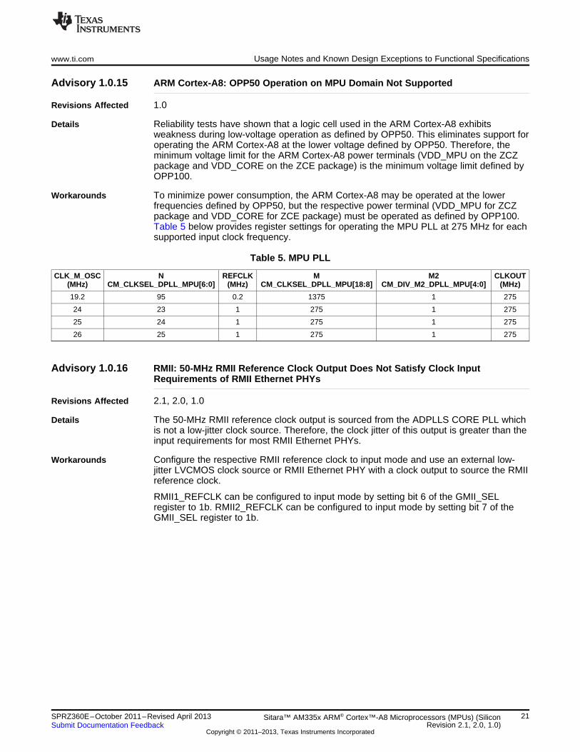
Workarounds To minimize power consumption, the ARM Cortex-A8 may be operated at the lowerfrequencies defined by OPP50, but the respective power terminal (VDD_MPU for ZCZpackage and VDD_CORE for ZCE package) must be operated as defined by OPP100.Table 5 below provides register settings for operating the MPU PLL at 275 MHz for eachsupported input clock frequency.
Table 5. MPU PLL
CLK_M_OSC N REFCLK M M2 CLKOUT(MHz) CM_CLKSEL_DPLL_MPU[6:0] (MHz) CM_CLKSEL_DPLL_MPU[18:8] CM_DIV_M2_DPLL_MPU[4:0] (MHz)
19.2 95 0.2 1375 1 275
24 23 1 275 1 275
25 24 1 275 1 275
26 25 1 275 1 275
Advisory 1.0.16 RMII: 50-MHz RMII Reference Clock Output Does Not Satisfy Clock InputRequirements of RMII Ethernet PHYs
Revisions Affected 2.1, 2.0, 1.0
Details The 50-MHz RMII reference clock output is sourced from the ADPLLS CORE PLL whichis not a low-jitter clock source. Therefore, the clock jitter of this output is greater than theinput requirements for most RMII Ethernet PHYs.
Workarounds Configure the respective RMII reference clock to input mode and use an external low-jitter LVCMOS clock source or RMII Ethernet PHY with a clock output to source the RMIIreference clock.
RMII1_REFCLK can be configured to input mode by setting bit 6 of the GMII_SELregister to 1b. RMII2_REFCLK can be configured to input mode by setting bit 7 of theGMII_SEL register to 1b.
21SPRZ360E–October 2011–Revised April 2013 Sitara™ AM335x ARM® Cortex™-A8 Microprocessors (MPUs) (SiliconRevision 2.1, 2.0, 1.0)Submit Documentation Feedback
Copyright © 2011–2013, Texas Instruments Incorporated

Usage Notes and Known Design Exceptions to Functional Specifications www.ti.com
Advisory 1.0.17 VDDS_DDR: High-Power Consumption During DeepSleep0
Revisions Affected 1.0
Details The REG_PHY_ENABLE_DYNAMIC PWRDN bit in the DDR_PHY_CTRL_1 registerprovides control for powering down the SSTL and HSTL input buffers to achieve lowerpower consumption from the VDDS_DDR power source. This register is reset to itsdefault value during DeepSleep0 which prevents powering down the DDR SSTL andHSTL input buffers which causes higher power consumption during DeepSleep0.
Workarounds Input buffers associated with the bi-directional DDR terminals can be configured tooperate as SSTL and HSTL or LVCMOS inputs. Low-power consumption can beachieved during DeepSleep0 by configuring the input buffers to operate in LVCMOSmode and enabling internal pull-downs on each of the bi-directional DDR terminalsbefore entering DeepSleep0. Power consumption from the VDDS_DDR power source ofthis solution is similar to powering down the DDR SSTL and HSTL input buffers.
The DDR PHY can be configured to operate in LVCMOS mode by setting theMDDR_SEL bit in the DDR_IO_CTRL register to 1b.
The internal pull-downs are configured by writing0011_1111_1111_0000_0000_00pp_pppp_pppp, where p = previous binary value, tothe DDR_DATA0_IOCTRL and DDR_DATA1_IOCTRL registers.
Advisory 1.0.18 ROM: Ethernet Boot Code Does Not Change Default Direction of RMII1 ReferenceClock When Booting from Ethernet Using RMII
Revisions Affected 1.0
Details The default direction of the RMII1 reference clock is output mode. This mode ofoperation is not supported, as described in Advisory 1.0.16.
When the SYSBOOT[7:6] boot mode inputs are set to 01b, which selects RMII mode,the RMII1_REF_CLK terminal is configured to operate in the non-supported output modeas soon as the ROM code changes the MUXMODE bits of the CONF_RMII1_REF_CLKregister from the default state of GPIO0_29 (111b) to RMII1_REFCLK (000b).
This causes contention on the RMII1 reference clock signal if the ROM code attempts toboot from RMII since the only RMII mode of operation supported requires theRMII1_REF_CLK terminal to be driven by an external 50-MHz RMII reference clocksource. Therefore, the ROM code must never be configured such that it attempts to bootfrom RMII.
Workarounds Use MII if Ethernet boot is required.
22 SPRZ360E–October 2011–Revised April 2013Sitara™ AM335x ARM® Cortex™-A8 Microprocessors (MPUs) (SiliconRevision 2.1, 2.0, 1.0) Submit Documentation Feedback
Copyright © 2011–2013, Texas Instruments Incorporated

www.ti.com Usage Notes and Known Design Exceptions to Functional Specifications
Advisory 1.0.19 DDR3: Fully-Automated Hardware READ and WRITE Leveling Not Supported
Revisions Affected 2.1, 2.0, 1.0
Details DDR3-based systems use a "fly-by" layout routing scheme where the address, clock,and control signals are connected to multiple memory devices using a daisy-chaintopology, as opposed to DDR2-based systems which connect multiple devices using abalanced T-topology. The "fly-by" routing scheme introduces skew in the arrival time ofthe DDR signals to each memory device. DDR3 memories and DDR3 memory controllerprovide hardware assisted training that optimizes timing for each data byte lane. This iscommonly referred to as READ and WRITE leveling. The objective of the READ andWRITE leveling is to obtain correct values of the DLL ratios to compensate for the skewand is done automatically during the initialization process.
The DDR3 controller does not reliably arrive at the optimal DLL ratios during theautomatic training process. Therefore, the automated hardware READ and WRITEleveling is not supported.
Workarounds Use the software-leveling procedure outlined below to obtain optimal DLL ratios thatcompensate READ and WRITE timing:
1. Disable automated hardware READ and WRITE leveling by setting theREG_RDWRLVL_EN bit in the RDWR_LVL_RMP_CTRL register to 0b.
2. Configure all EMIF4D registers, including AC timing values, as required for theattached DDR3 memory device.
3. Determine the initial seed DLL ratio values to be used in the software-levelingalgorithm. These values are based on board trace lengths of DDR_CK(n) andDDR_DQS(n).
4. Run the software-leveling algorithm with the initial seed DLL ratio values. Thealgorithm iterates several times to find the optimum values for the givenconfiguration.
5. The software-leveling algorithm determines the optimum values for the followingregisters in the DDR controller. Use the optimum values obtained from the programwhen initializing the DDR controller.
• DATA_PHY_RD_DQS_SLAVE_RATIO
• DATA_PHY_FIFO_WE_SLAVE_RATIO
• DATA_PHY_WR_DQS_SLAVE_RATIO
• DATA_PHY_WR_DATA_SLAVE_RATIO
This procedure is only required once for a given combination of DDR3 memory devices,DDR3 operating frequency, and printed circuit board layout. If there are any changes tomemory devices, operating frequency, or printed circuit board layout, the procedureoutlined above must be re-run.
23SPRZ360E–October 2011–Revised April 2013 Sitara™ AM335x ARM® Cortex™-A8 Microprocessors (MPUs) (SiliconRevision 2.1, 2.0, 1.0)Submit Documentation Feedback
Copyright © 2011–2013, Texas Instruments Incorporated

Usage Notes and Known Design Exceptions to Functional Specifications www.ti.com
Advisory 1.0.20 Boot: USB Boot ROM Code Overlapping Data in TXFIFO and RXFIFO
Revisions Affected 1.0
Details The USB boot ROM code is overlapping data in the TXFIFO and RXFIFO which leads todata corruption. This data corruption causes a data abort and prevents USB boot fromworking.
Workarounds There is no workaround for this issue.
Advisory 1.0.21 SmartReflex: Limited Support Due to Issue Described in Advisory 1.0.15
Revisions Affected 1.0
Details SmartReflex is not supported on the VDD_MPU power domain of the ZCZ packagewhen configured for OPP100 because SmartReflex may reduce the VDD_MPU voltageto OPP50 levels. Advisory 1.0.15 describes why operating the ARM Cortex-A8 at thelower voltage defined by OPP50 is not supported. For more details related to this issue,see Advisory 1.0.15.
SmartReflex is not supported on the ZCE package.
SmartReflex is supported on the ZCZ package for the following power domain and OPPcombinations:
• VDD_CORE configured for OPP100.
• VDD_MPU configured for any valid OPP greater than OPP100.
Workarounds There is no workaround for this issue.
24 SPRZ360E–October 2011–Revised April 2013Sitara™ AM335x ARM® Cortex™-A8 Microprocessors (MPUs) (SiliconRevision 2.1, 2.0, 1.0) Submit Documentation Feedback
Copyright © 2011–2013, Texas Instruments Incorporated

www.ti.com Usage Notes and Known Design Exceptions to Functional Specifications
Advisory 1.0.22 EMIF: Dynamic Voltage Frequency Scaling (DVFS) is Not Supported
Revisions Affected 2.1, 2.0, 1.0
Details The L3 Interconnect and EMIF internal hookup does not allow changing the EMIFoperating frequency while OCP transactions are pending. This prevents dynamicswitching from OPP100 to OPP50 or from OPP50 to OPP100. The application softwaremust initialize a static OPP50 or OPP100 configuration before enabling EMIF.
Workarounds There is no workaround for this issue.
Advisory 1.0.23 Ethernet Media Access Controller and Switch Subsystem: Reset Isolation Featureis Not Supported
Revisions Affected 2.1, 2.0, 1.0
Details The Ethernet Media Access Controller and Switch (CPSW) subsystem may lock up if theReset Isolation feature is enabled when a warm reset is applied while the host port istransmitting data. Since most warm reset sources can be asynchronous events, thislock-up condition can only be prevented by not enabling this feature.
The Reset Isolation feature is not enabled by default.
Workarounds There is no workaround for this issue.
25SPRZ360E–October 2011–Revised April 2013 Sitara™ AM335x ARM® Cortex™-A8 Microprocessors (MPUs) (SiliconRevision 2.1, 2.0, 1.0)Submit Documentation Feedback
Copyright © 2011–2013, Texas Instruments Incorporated

Usage Notes and Known Design Exceptions to Functional Specifications www.ti.com
Advisory 1.0.24 Boot: System Boot is Not Reliable if Reset is Asserted While Operating in OPP50
Revisions Affected 2.1, 2.0, 1.0
Details The system attempts to boot using the ARM (A8), L3, L4, and respective DDR clockfrequencies defined by OPP100 when a reset is asserted. The system may fail to boot ifthe system is operating with reduced VDD_MPU and VDD_CORE power supply voltagesas defined by OPP50 when reset is asserted. This issue occurs because the device isbeing operated at OPP100 clock frequencies with OPP50 supply voltages. Thisunsupported operating condition potentially over-clocks the logic which was only timingclosed to operate at OPP50 clock frequencies with OPP50 supply voltages.
There are three basic reset sources, the PWRONRSTn terminal, the WARMRSTnterminal, and the internal watchdog timer, that need to be considered when designing aproduct that supports OPP50.
It is important to return VDD_MPU and VDD_CORE power supplies to OPP100 definedvoltages before any of these resets sources are asserted.
Workarounds Only source the PWRONRSTn terminal from a power management circuit that alwaysreturns VDD_MPU and VDD_CORE power supplies to OPP100 defined voltages beforeasserting PWRONRSTn.
There are two possible workarounds that can be applied to the other two reset sources.The first workaround provides the lowest power consumption option but eliminates thewatchdog timer and WARMRSTn terminal functions. The second workaround retains thewatchdog timer and WARMRSTn terminal functions, but causes the device to consumehigher power.
• Disable the watchdog timer and do not assert the WARMRSTn terminal while theVDD_MPU and VDD_CORE power supply voltages are less than those defined byOPP100.
• Retain the VDD_MPU and VDD_CORE power supply voltages defined by OPP100while operating the ARM (A8), L3, L4, and the respective DDR clocks at the reducedfrequencies defined by OPP50.
26 SPRZ360E–October 2011–Revised April 2013Sitara™ AM335x ARM® Cortex™-A8 Microprocessors (MPUs) (SiliconRevision 2.1, 2.0, 1.0) Submit Documentation Feedback
Copyright © 2011–2013, Texas Instruments Incorporated

www.ti.com Usage Notes and Known Design Exceptions to Functional Specifications
Advisory 1.0.25 Boot: System Boot Temporarily Stalls if an Attempt to Boot from Ethernet is NotSuccessful
Revisions Affected 2.1, 2.0, 1.0
Details The system is delayed for up to 4.5 minutes before continuing to the next boot device ifan attempt to boot from Ethernet fails for any reason.
This delay is likely to cause an undesirable user experience when the boot sequenceattempts Ethernet boot before booting from the primary boot device. For example, it maybe desirable to select SYSBOOT [4:0] = 00111b for a product that would normally skipover Ethernet boot which is the first boot device in this sequence and boots from MMC0which is the second boot device in this sequence. This example boot sequence providesan option to boot from Ethernet as a way to break into the boot sequence to updateMMC0 boot code by simply connecting it to an Ethernet host capable of booting theproduct for the purpose of updating MMC0 boot code. However, this boot sequenceattempts to boot from Ethernet first which would insert an undesirable long delay whenbooting from MMC0.
Workarounds There is no device-level workaround, but it may be possible to develop a system-levelsolution that mitigates the effect of this issue when an occasional Ethernet boot isrequired. In the example described above, the system could be designed with the bootsequence defined by SYSBOOT [4:0] = 11001b which attempts to boot from MMC0before Ethernet. This does not provide a default method to break into the boot sequencewith Ethernet boot, but the product could be designed with a switch that temporarilydisables MMC0 boot as a way to invoke Ethernet boot. The switch would only be used totemporarily disable MMC0 while the product boots from Ethernet. Once the product hasbooted from Ethernet, the switch would be returned to its normal operating mode beforethe MMC0 boot code is updated.
27SPRZ360E–October 2011–Revised April 2013 Sitara™ AM335x ARM® Cortex™-A8 Microprocessors (MPUs) (SiliconRevision 2.1, 2.0, 1.0)Submit Documentation Feedback
Copyright © 2011–2013, Texas Instruments Incorporated

Usage Notes and Known Design Exceptions to Functional Specifications www.ti.com
Advisory 1.0.26 I2C: SDA and SCL Open-Drain Output Buffer Issue
Revisions Affected 2.0, 1.0
Details The I2Cx_SDA and I2Cx_SCL outputs are implemented with push-pull 3-state outputbuffers rather than open-drain output buffers as required by I2C. While it is possible forthe push-pull 3-state output buffers to behave as open-drain outputs, an internal timingskew issue causes the outputs to drive a logic-high for a duration of (0–5 ns) before theoutputs are disabled. The unexpected high-level pulse will only occur when the SCL orSDA outputs transition from a driven low state to a high-impedance state and there issufficient internal timing skew on the respective I2C output.
This short high-level pulse injects energy in the I2C signals traces, which causes the I2Csignals to sustain a period of ringing as a result of multiple transmission line reflections.This ringing should not cause an issue on the SDA signal because it only occurs at timeswhen SDA is expected to be changing logic levels and the ringing will have time to dampbefore data is latched by the receiving device. The ringing may have enough amplitudeto cross the SCL input buffer switching threshold several times during the first fewnanoseconds of this ringing period, which may cause clock glitches. This ringing shouldnot cause a problem if the amplitude is damped within the first 50 ns because I2Cdevices are required to filter their SCL inputs to remove clock glitches. Therefore, it isimportant to design the PCB signal traces to limit the duration of the ringing to less than50 ns. One possible solution is to insert series termination resistors near the AM335xSCL and SDA terminals to attenuate transmission line reflections.
This issue may also cause the SDA output to be in contention with the slave SDA outputfor the duration of the unexpected high-level pulse when the slave begins its ACK cycle.This occurs because the slave may already be driving SDA low before the unexpectedhigh-level pulse occurs. The glitch that occurs on SDA as a result of this short period ofcontention does not cause any I2C protocol issue but the peak current applies unwantedstress to both I2C devices and potentially increases power supply noise. Therefore, aseries termination resistor located near the respective AM335x SDA terminal is requiredto limit the current during the short period of contention.
A similar contention problem can occur on SCL when connected to I2C slave devicesthat support clock stretching. This occurs because the slave is driving SCL low beforethe unexpected high-level pulse occurs. The glitch that occurs on SCL as a result of thisshort period of contention does not cause any I2C protocol issue because I2C devicesare required to apply a glitch filter to their SCL inputs. However, the peak current appliesunwanted stress to both I2C devices and potentially increases power supply noise.Therefore, a series termination resistor located near the respective AM335x SCLterminal is required to limit the current during the short period of contention.
If another master is connected, the unexpected high-level pulses on the SCL and SDAoutputs can cause contention during clock synchronization and arbitration. The seriestermination resistors described above will also limit the contention current in this usecase without creating any I2C protocol issue.
Workarounds Insert series termination resistors on the SCL and SDA signals and locate them near theAM335x SCL and SDA terminals. The SCL and SDA pullup resistors should also belocated near the AM335x SCL and SDA terminals. The placement of the seriestermination resistor and pullup resistor should be connected as shown in Figure 4.
28 SPRZ360E–October 2011–Revised April 2013Sitara™ AM335x ARM® Cortex™-A8 Microprocessors (MPUs) (SiliconRevision 2.1, 2.0, 1.0) Submit Documentation Feedback
Copyright © 2011–2013, Texas Instruments Incorporated

I2C
Signal Traces ConnectingOther I2C DevicesVDDSHVx
Rpu
Rst
I2Cx_SCLI2Cx_SDA
AM335x
I2C
I2C
www.ti.com Usage Notes and Known Design Exceptions to Functional Specifications
Figure 4. Placement of Series Termination Resistor and Pullup Resistor
Table 6 provides series termination and pullup resistor value recommendations. The I2Csignal level and respective VDDSHVx power supply voltage is shown in the first column.Two resistor value combination options are provided for each voltage. One optionsupports a maximum high-level input current of 200 uA to all attached I2C devices, whilethe other option supports a maximum high-level input current of 100 uA to all attachedI2C devices.
Table 6. Recommended Values for Series Termination Resistor and Pullup Resistor
I2C SIGNAL LEVEL AND SERIES TERMINATIONRESPECTIVE VDDSHVx PULLUP RESISTOR (Ω) NOTESRESISTOR (Ω)POWER SUPPLY (V)
Maximum high-level input1.8 60 1500 current up to 200 µA
Maximum high-level input1.8 75 3300 current up to 100 µA
Maximum high-level input3.3 60 3300 current up to 200 µA
Maximum high-level input3.3 75 6600 current up to 100 µA
29SPRZ360E–October 2011–Revised April 2013 Sitara™ AM335x ARM® Cortex™-A8 Microprocessors (MPUs) (SiliconRevision 2.1, 2.0, 1.0)Submit Documentation Feedback
Copyright © 2011–2013, Texas Instruments Incorporated

Usage Notes and Known Design Exceptions to Functional Specifications www.ti.com
Advisory 1.0.27 LCDC: LIDD DMA Mode Issue
Revisions Affected 2.1, 2.0, 1.0
Details After a DMA transfer is complete, the LIDD_DMA_EN bit in the LIDD_CTRL register isdriven low and the read/write pointers of the Asynchronous FIFO are designed to reset.However, only the write pointer gets reset and, therefore, the FIFO sequence is corrupt.This could cause flickering or tearing of images being displayed on an LCD.
Workarounds After each DMA transfer, wait for Done interrupt by polling the DONE_RAW_SET bit inthe IRQSTATUS_RAW register, and then write 1 to the DMA_RST and LIDD_RST bitsin the CLKC_RESET register to perform software reset of the L3 and LIDD clockdomains. This returns the write and read FIFO pointers to their default values and allowsfor proper FIFO operation.
This workaround has a side effect that needs to be considered. The LCDC drives theLCD control signals to their active state when software reset is asserted if the activestates of the LCD panel inputs are opposite the LCDC default states. If this is the case, itmay be necessary to add a hardware isolation circuit to the LCD panel chip select signalthat disconnects the LCDC output from the LCD panel input before the software reset isasserted. The LCDC output could be reconnected to the LCD panel input after LCDChas been re-initialized. An example isolation circuit may be a single channel bus FETswitch inserted in the chip select signal path with the enable being controlled by a GPIO.The LCD panel input would need a pull-up or pull-down resistor to force an inactive statewhile the switch is open.
30 SPRZ360E–October 2011–Revised April 2013Sitara™ AM335x ARM® Cortex™-A8 Microprocessors (MPUs) (SiliconRevision 2.1, 2.0, 1.0) Submit Documentation Feedback
Copyright © 2011–2013, Texas Instruments Incorporated

www.ti.com Usage Notes and Known Design Exceptions to Functional Specifications
Advisory 1.0.28 LCDC: Raster Mode, Hardware Auto Underflow Restart Does Not Work
Revisions Affected 2.1, 2.0, 1.0
Details The hardware restart of the LCDC during a FIFO underflow condition does not work.Setting the AUTO_UFLOW_RESTART bit in the LCDC control register has no effect.
Workarounds This functionality can be implemented using the software reset method outlined inSection 13.4.6, Disable and Software Reset Sequence, of the AM335x ARM Cortex-A8Microprocessors (MPUs) Technical Reference Manual (literature number SPRUH73).
Below are the summarized steps to perform a software reset:
1. Write 0 to the LCDEN bit in the RASTER_CTRL register.
2. Wait for Done interrupt by polling the DONE_RAW_SET bit in the IRQSTATUS_RAWregister.
3. Write 1 to the MAIN_RST, or DMA_RST and CORE_RST bits in the CLKC_RESETregister.
4. Wait several clock cycles.
5. Write 0 to the MAIN_RST, or DMA_RST and CORE_RST bits in the CLKC_RESETregister.
6. Write 1 to the LCDEN bit in the RASTER_CTRL register.
Advisory 1.0.29 Latch-up Performance: Latch-up Performance Limits for Silicon Revsions 1.0 and2.0
Revisions Affected 2.0, 1.0
Details Latch-up performance was improved in silicon revision 2.1 devices and the new limitshave been updated in revision F of the AM335x ARM Cortex-A8 Microprocessors(MPUs) data manual (literature number SPRS717).
Table 7 provides latch-up performance limits published in previous revisions of theAM335x data manual and these limits apply to silicon revisions 1.0 and 2.0.
Table 7. Latch-up Performance Limits - Silicon Revisions 1.0 and 2.0
PARAMETER MIN MAX UNITS
Latch-up Performance Class II (105°C) 25 mA
Workarounds Not applicable.
31SPRZ360E–October 2011–Revised April 2013 Sitara™ AM335x ARM® Cortex™-A8 Microprocessors (MPUs) (SiliconRevision 2.1, 2.0, 1.0)Submit Documentation Feedback
Copyright © 2011–2013, Texas Instruments Incorporated

Revision History www.ti.com
Revision History
Changes from D Revision (February 2013) to E Revision ............................................................................................. Page
• Modified Table 1, Production Device Revision Codes ............................................................................... 5• Modified Table 2, Silicon Revision Variables ......................................................................................... 5• Modified Table 3, All Usage Notes ..................................................................................................... 6• Modified Table 4, All Design Exceptions to Functional Specifications ............................................................ 6• Deleted McASP0 and McASP1 list items in Section 3.1.5, Pin Multiplexing: Valid IO Sets and Restrictions .............. 10• Added 2.1 to Revision Affected on all applicable Advisories ...................................................................... 12• Added Advisory 1.0.29, Latch-up Performance: Latch-up Performance Limits for Silicon Revsions 1.0 and 2.0 .......... 31
NOTE: Page numbers for previous revisions may differ from page numbers in the current version.
32 Revision History SPRZ360E–October 2011–Revised April 2013Submit Documentation Feedback
Copyright © 2011–2013, Texas Instruments Incorporated

IMPORTANT NOTICE
Texas Instruments Incorporated and its subsidiaries (TI) reserve the right to make corrections, enhancements, improvements and otherchanges to its semiconductor products and services per JESD46, latest issue, and to discontinue any product or service per JESD48, latestissue. Buyers should obtain the latest relevant information before placing orders and should verify that such information is current andcomplete. All semiconductor products (also referred to herein as “components”) are sold subject to TI’s terms and conditions of salesupplied at the time of order acknowledgment.
TI warrants performance of its components to the specifications applicable at the time of sale, in accordance with the warranty in TI’s termsand conditions of sale of semiconductor products. Testing and other quality control techniques are used to the extent TI deems necessaryto support this warranty. Except where mandated by applicable law, testing of all parameters of each component is not necessarilyperformed.
TI assumes no liability for applications assistance or the design of Buyers’ products. Buyers are responsible for their products andapplications using TI components. To minimize the risks associated with Buyers’ products and applications, Buyers should provideadequate design and operating safeguards.
TI does not warrant or represent that any license, either express or implied, is granted under any patent right, copyright, mask work right, orother intellectual property right relating to any combination, machine, or process in which TI components or services are used. Informationpublished by TI regarding third-party products or services does not constitute a license to use such products or services or a warranty orendorsement thereof. Use of such information may require a license from a third party under the patents or other intellectual property of thethird party, or a license from TI under the patents or other intellectual property of TI.
Reproduction of significant portions of TI information in TI data books or data sheets is permissible only if reproduction is without alterationand is accompanied by all associated warranties, conditions, limitations, and notices. TI is not responsible or liable for such altereddocumentation. Information of third parties may be subject to additional restrictions.
Resale of TI components or services with statements different from or beyond the parameters stated by TI for that component or servicevoids all express and any implied warranties for the associated TI component or service and is an unfair and deceptive business practice.TI is not responsible or liable for any such statements.
Buyer acknowledges and agrees that it is solely responsible for compliance with all legal, regulatory and safety-related requirementsconcerning its products, and any use of TI components in its applications, notwithstanding any applications-related information or supportthat may be provided by TI. Buyer represents and agrees that it has all the necessary expertise to create and implement safeguards whichanticipate dangerous consequences of failures, monitor failures and their consequences, lessen the likelihood of failures that might causeharm and take appropriate remedial actions. Buyer will fully indemnify TI and its representatives against any damages arising out of the useof any TI components in safety-critical applications.
In some cases, TI components may be promoted specifically to facilitate safety-related applications. With such components, TI’s goal is tohelp enable customers to design and create their own end-product solutions that meet applicable functional safety standards andrequirements. Nonetheless, such components are subject to these terms.
No TI components are authorized for use in FDA Class III (or similar life-critical medical equipment) unless authorized officers of the partieshave executed a special agreement specifically governing such use.
Only those TI components which TI has specifically designated as military grade or “enhanced plastic” are designed and intended for use inmilitary/aerospace applications or environments. Buyer acknowledges and agrees that any military or aerospace use of TI componentswhich have not been so designated is solely at the Buyer's risk, and that Buyer is solely responsible for compliance with all legal andregulatory requirements in connection with such use.
TI has specifically designated certain components as meeting ISO/TS16949 requirements, mainly for automotive use. In any case of use ofnon-designated products, TI will not be responsible for any failure to meet ISO/TS16949.
Products Applications
Audio www.ti.com/audio Automotive and Transportation www.ti.com/automotive
Amplifiers amplifier.ti.com Communications and Telecom www.ti.com/communications
Data Converters dataconverter.ti.com Computers and Peripherals www.ti.com/computers
DLP® Products www.dlp.com Consumer Electronics www.ti.com/consumer-apps
DSP dsp.ti.com Energy and Lighting www.ti.com/energy
Clocks and Timers www.ti.com/clocks Industrial www.ti.com/industrial
Interface interface.ti.com Medical www.ti.com/medical
Logic logic.ti.com Security www.ti.com/security
Power Mgmt power.ti.com Space, Avionics and Defense www.ti.com/space-avionics-defense
Microcontrollers microcontroller.ti.com Video and Imaging www.ti.com/video
RFID www.ti-rfid.com
OMAP Applications Processors www.ti.com/omap TI E2E Community e2e.ti.com
Wireless Connectivity www.ti.com/wirelessconnectivity
Mailing Address: Texas Instruments, Post Office Box 655303, Dallas, Texas 75265Copyright © 2013, Texas Instruments Incorporated