15
SSD (Solid State Disk) http://en.wikipedia.org/wiki/Solid-state_drive
SSD
(Solid State Disk)http://en.wikipedia.org/wiki/Solid-state_drive
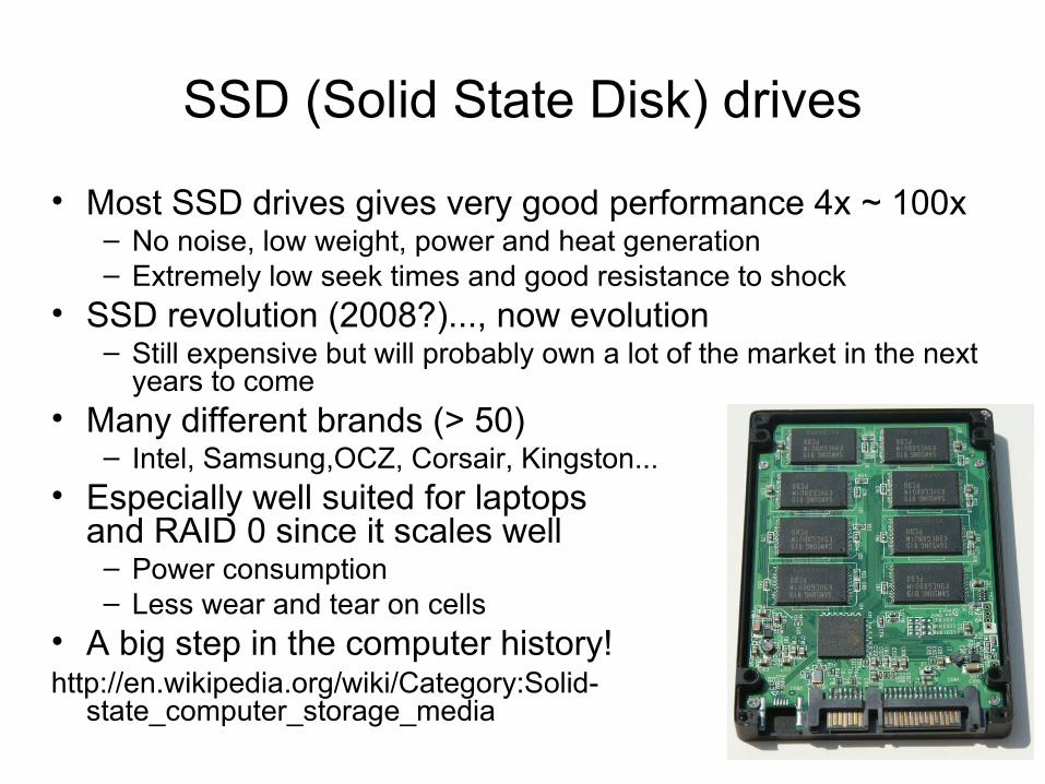
SSD (Solid State Disk) drives
• Most SSD drives gives very good performance 4x ~ 100x– No noise, low weight, power and heat generation– Extremely low seek times and good resistance to shock
• SSD revolution (2008?)..., now evolution – Still expensive but will probably own a lot of the market in the next
years to come• Many different brands (> 50)
– Intel, Samsung,OCZ, Corsair, Kingston...• Especially well suited for laptops
and RAID 0 since it scales well– Power consumption– Less wear and tear on cells
• A big step in the computer history!http://en.wikipedia.org/wiki/Category:Solid-
state_computer_storage_media
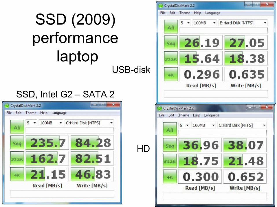
SSD (2009) performance
laptop
HD
USB-disk
SSD, Intel G2 – SATA 2
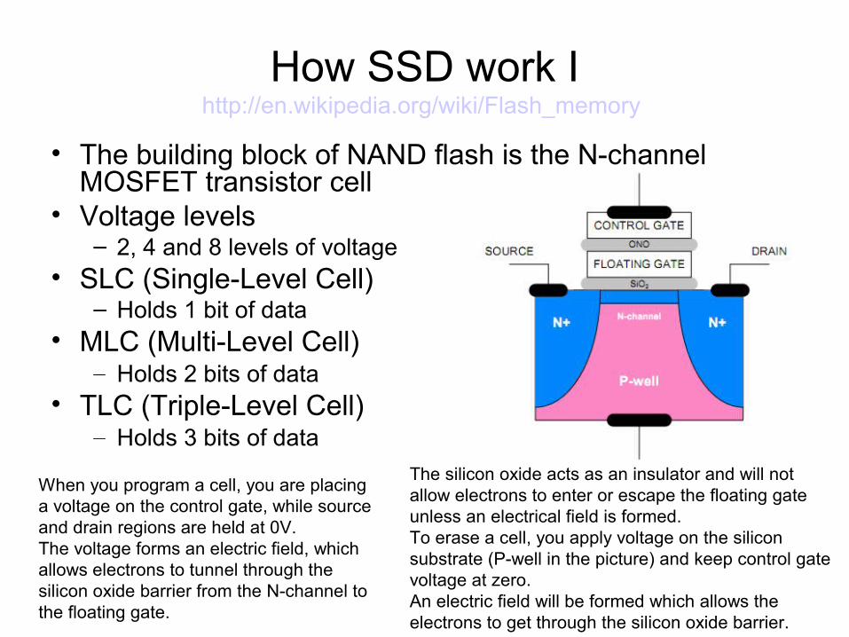
How SSD work Ihttp://en.wikipedia.org/wiki/Flash_memory
• The building block of NAND flash is the N-channel MOSFET transistor cell
• Voltage levels– 2, 4 and 8 levels of voltage
• SLC (Single-Level Cell)– Holds 1 bit of data
• MLC (Multi-Level Cell)– Holds 2 bits of data
• TLC (Triple-Level Cell)– Holds 3 bits of data
When you program a cell, you are placing a voltage on the control gate, while source and drain regions are held at 0V.The voltage forms an electric field, which allows electrons to tunnel through the silicon oxide barrier from the N-channel to the floating gate.
The silicon oxide acts as an insulator and will not allow electrons to enter or escape the floating gate unless an electrical field is formed. To erase a cell, you apply voltage on the silicon substrate (P-well in the picture) and keep control gate voltage at zero. An electric field will be formed which allows the electrons to get through the silicon oxide barrier.
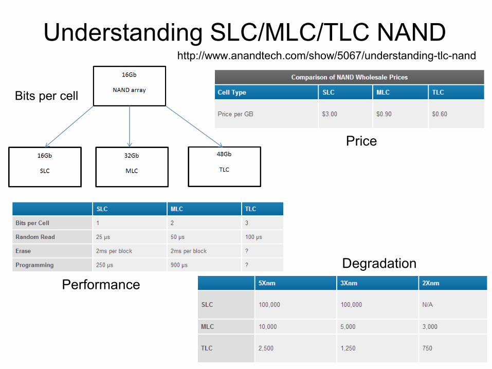
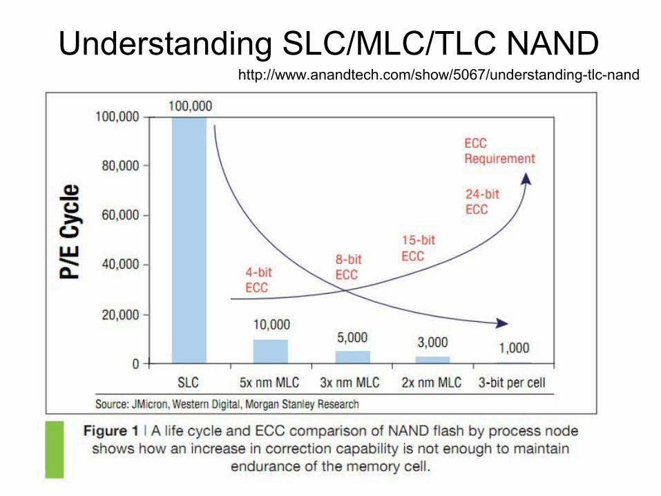
Understanding SLC/MLC/TLC NANDhttp://www.anandtech.com/show/5067/understanding-tlc-nand
Degradation
Performance
Bits per cell
Price
Understanding SLC/MLC/TLC NANDhttp://www.anandtech.com/show/5067/understanding-tlc-nand
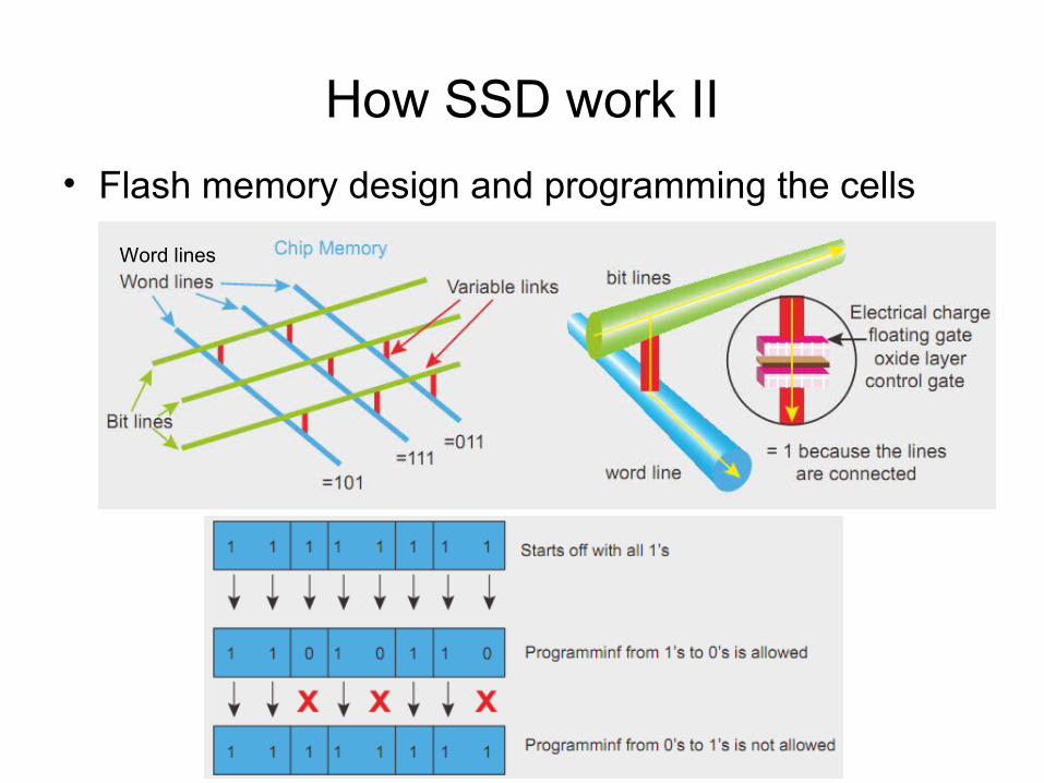
How SSD work II
Word lines
• Flash memory design and programming the cells
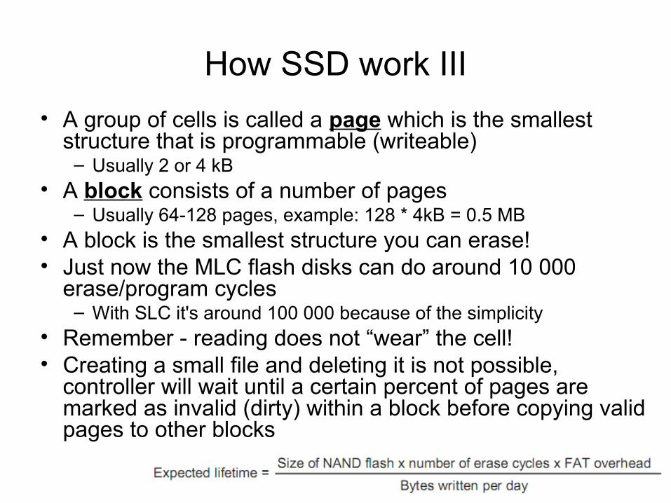
How SSD work III
• A group of cells is called a page which is the smallest structure that is programmable (writeable)
– Usually 2 or 4 kB• A block consists of a number of pages
– Usually 64-128 pages, example: 128 * 4kB = 0.5 MB• A block is the smallest structure you can erase!• Just now the MLC flash disks can do around 10 000
erase/program cycles– With SLC it's around 100 000 because of the simplicity
• Remember - reading does not “wear” the cell!• Creating a small file and deleting it is not possible,
controller will wait until a certain percent of pages are marked as invalid (dirty) within a block before copying valid pages to other blocks
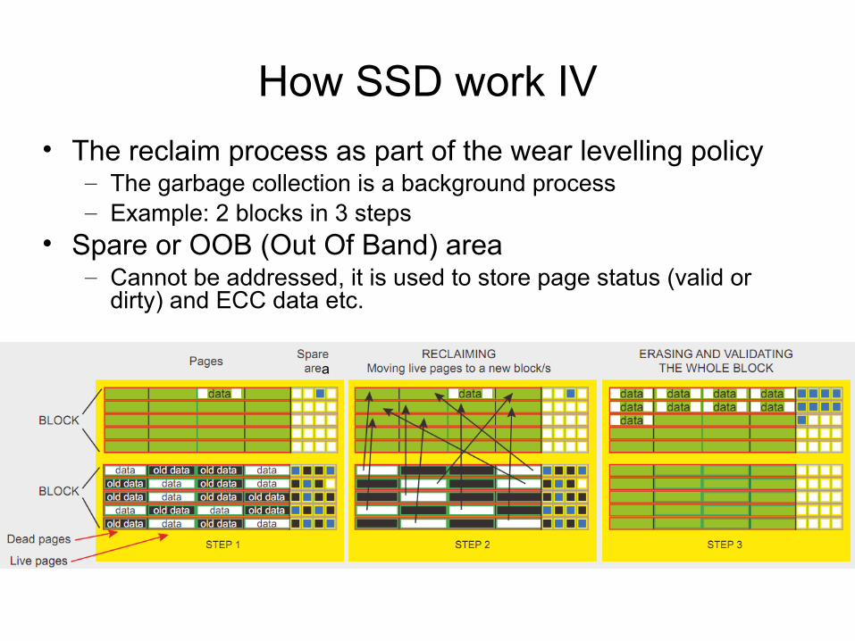
How SSD work IV
• The reclaim process as part of the wear levelling policy– The garbage collection is a background process – Example: 2 blocks in 3 steps
• Spare or OOB (Out Of Band) area– Cannot be addressed, it is used to store page status (valid or
dirty) and ECC data etc.
a
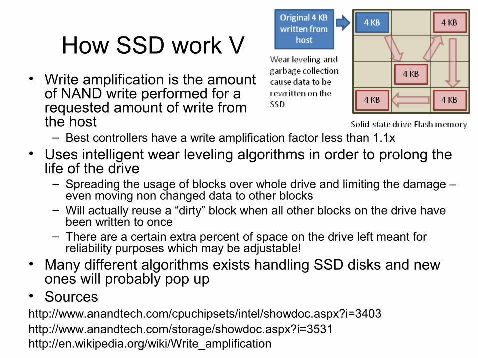
How SSD work V• Write amplification is the amount
of NAND write performed for a requested amount of write from the host
– Best controllers have a write amplification factor less than 1.1x• Uses intelligent wear leveling algorithms in order to prolong the
life of the drive– Spreading the usage of blocks over whole drive and limiting the damage –
even moving non changed data to other blocks– Will actually reuse a “dirty” block when all other blocks on the drive have
been written to once– There are a certain extra percent of space on the drive left meant for
reliability purposes which may be adjustable!• Many different algorithms exists handling SSD disks and new
ones will probably pop up• Sourceshttp://www.anandtech.com/cpuchipsets/intel/showdoc.aspx?i=3403http://www.anandtech.com/storage/showdoc.aspx?i=3531http://en.wikipedia.org/wiki/Write_amplification
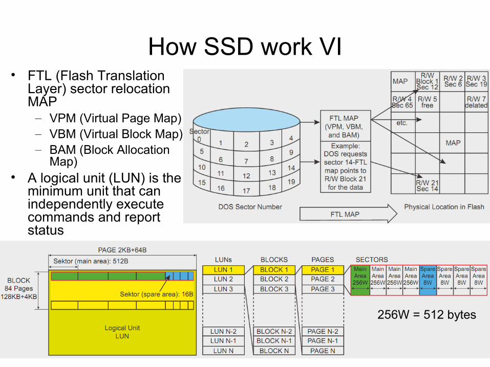
How SSD work VI• FTL (Flash Translation
Layer) sector relocation MAP– VPM (Virtual Page Map)– VBM (Virtual Block Map)– BAM (Block Allocation
Map)• A logical unit (LUN) is the
minimum unit that can independently execute commands and report status
256W = 512 bytes
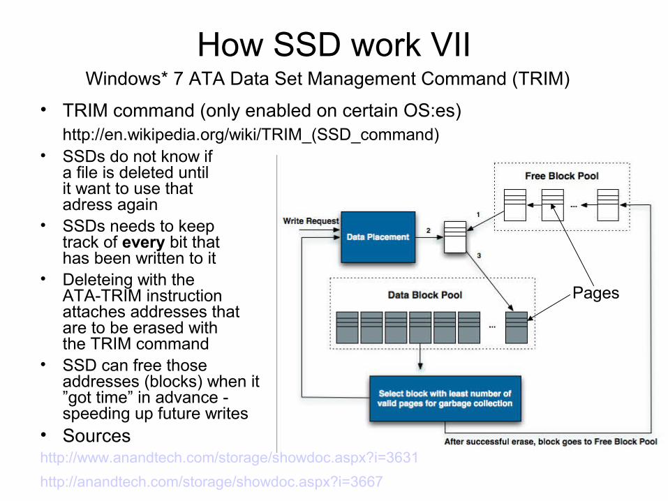
How SSD work VII
• TRIM command (only enabled on certain OS:es)http://en.wikipedia.org/wiki/TRIM_(SSD_command)
• SSDs do not know if a file is deleted until it want to use that adress again
• SSDs needs to keeptrack of every bit that has been written to it
• Deleteing with the ATA-TRIM instruction attaches addresses that are to be erased with the TRIM command
• SSD can free thoseaddresses (blocks) when it ”got time” in advance - speeding up future writes
• Sourceshttp://www.anandtech.com/storage/showdoc.aspx?i=3631
http://anandtech.com/storage/showdoc.aspx?i=3667
Windows* 7 ATA Data Set Management Command (TRIM)
Pages
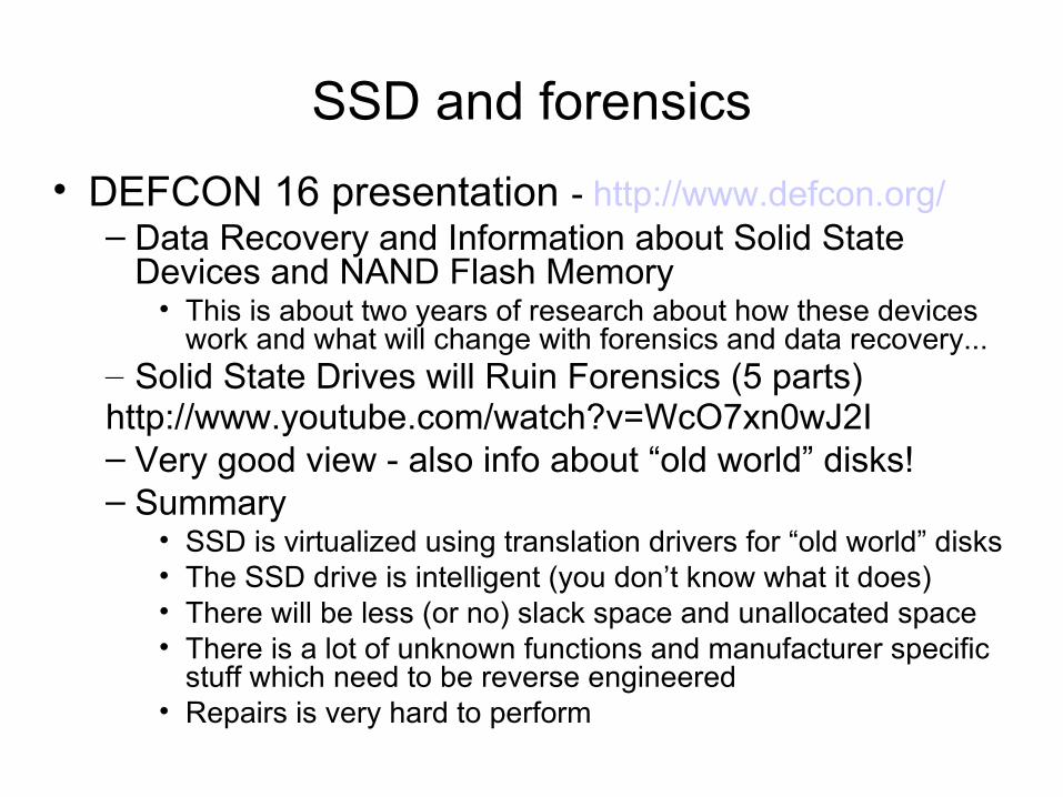
SSD and forensics
• DEFCON 16 presentation - http://www.defcon.org/– Data Recovery and Information about Solid State
Devices and NAND Flash Memory • This is about two years of research about how these devices
work and what will change with forensics and data recovery...– Solid State Drives will Ruin Forensics (5 parts)http://www.youtube.com/watch?v=WcO7xn0wJ2I– Very good view - also info about “old world” disks!– Summary
• SSD is virtualized using translation drivers for “old world” disks• The SSD drive is intelligent (you don’t know what it does)• There will be less (or no) slack space and unallocated space• There is a lot of unknown functions and manufacturer specific
stuff which need to be reverse engineered• Repairs is very hard to perform
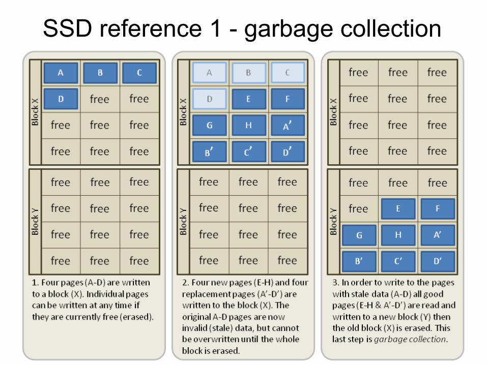
SSD reference 1 - garbage collection
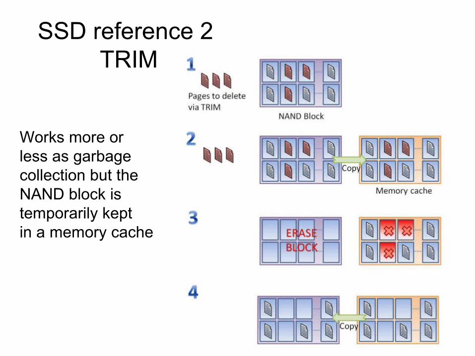
SSD reference 2 TRIM
Works more or less as garbage collection but theNAND block is temporarily kept in a memory cache


![JEDEC SSD Specifications Explained [Compatibility Mode]_0.pdf · JEDEC SSD Standards ‣JESD218, Solid State Drive (SSD) Requirements and Endurance Test Method ‣JESD219, Solid State](https://static.documents.pub/doc/80x56/5be0a70f09d3f284588c4801/jedec-ssd-specifications-compatibility-mode0pdf-jedec-ssd-standards-jesd218.jpg)


