Page 1
Sitronix Technology Corp. reserves the right to change the contents in this document without prior notice.
ST7775R 176RGB x 220 dot 262K Color with Frame Memory
Single-Chip TFT Controller/Driver
Datasheet Preliminary Version 0.1 2010/03
Page 2
ST7775R
Version 0.1 Page 2 of 128 2010/03
LIST OF CONTENT 1 GENERAL DESCRIPTION..................................................................... 8
2 FEATURES ............................................................................................ 9
3 PAD ARRANGEMENT ......................................................................... 11
3.1.. Pad Arrangement...............................................................................................11
3.2.. Bump Dimension ...............................................................................................12
3.3.. Alignment Mark Dimension................................................................................13
3.4.. Chip Information ................................................................................................13
4 PAD CENTER COORDINATES ........................................................... 14
5 BLOCK DIAGRAM ............................................................................... 29
6 PIN DESCRIPTION .............................................................................. 30
6.1.. Power Supply Pins.............................................................................................30
6.2.. Interface Logic Pins ...........................................................................................31
6.3.. Driver Output Pins .............................................................................................33
6.4.. Test Pins............................................................................................................34
7 DRIVER ELECTRICAL CHARACTERISTICS...................................... 35
7.1.. Absolute Operation Range ................................................................................35
7.2.. DC Characteristics.............................................................................................36
7.3.. Power Consumption ..........................................................................................37
7.4.. AC Characteristics .............................................................................................38
7.4.1 8080 Series MCU Parallel Interface Characteristics: 18/16/9/8-bit Bus ...................... 38
7.4.2 6800 Series MCU Parallel Interface Characteristics: 18/16/9/8-bit Bus ...................... 40
7.4.3 Serial Data Transfer Interface Characteristics: ............................................................. 41
7.4.4 RGB Interface Characteristics: ....................................................................................... 42
8 INTERFACE ......................................................................................... 44
8.1.. MCU Interface Type Selection...........................................................................44
8.2.. 8080-Series MCU Write Cycle Sequence..........................................................45
8.3.. 6800-Series MCU Write Cycle Sequence..........................................................46
8.3.1 18 bits Interface Write Data Format................................................................................ 47
8.3.2 16 bits Interface Write Data Format................................................................................ 48
8.3.3 9 bits Interface Write Data Format .................................................................................. 49
8.3.4 8 bits Interface Write Data Format .................................................................................. 51
8.3.5 8080-series MCU Read Cycle Sequence ........................................................................ 53
8.3.6 6800-series MCU Read Cycle Sequence ........................................................................ 54
8.3.7 18bits interface read data format.................................................................................... 55
8.3.8 16bits Interface Read Data Format ................................................................................. 56
8.3.9 9bits Interface Read Data Format ................................................................................... 57
8.3.10 8bits Interface Read Data Format ................................................................................... 58
Page 3
ST7775R
Version 0.1 Page 3 of 128 2010/03
8.4.. RGB Input Interface ...........................................................................................60
8.4.1 RGB Interface ................................................................................................................... 61
8.4.2 RGB Interface Timing....................................................................................................... 62
8.4.3 Moving Picture Mode ....................................................................................................... 64
8.4.4 6-bit RGB Interface........................................................................................................... 66
8.4.5 16-bit RGB Interface......................................................................................................... 67
8.4.6 18-bit RGB Interface......................................................................................................... 68
8.5.. Interface Timing .................................................................................................71
8.6.. 24-bit Serial Peripheral Interface (24-bit SPI) ....................................................72
8.7.. 9-bit Serial Peripheral Interface (9-bit SPI) ........................................................76
8.8.. 8-bit Serial Peripheral Interface (8-bit SPI) ........................................................78
8.9.. Data Transfer Recovery.....................................................................................80
8.10.. Register Descriptions.........................................................................................80
9 COMMAND........................................................................................... 84
9.1.. System Function Command List ........................................................................84
9.2.. System Function Command...............................................................................86
9.2.1 Index (IR) ........................................................................................................................... 86
9.2.2 Device ID Code Read (R00h) ........................................................................................... 86
9.2.3 Device Output Control (R01h) ......................................................................................... 86
9.2.4 LCD Driving Wave Control (R02h) .................................................................................. 88
9.2.5 Entry Mode (R03h)............................................................................................................ 89
9.2.6 Display Control 1 (R07h).................................................................................................. 92
9.2.7 Display Control 2 (R08h).................................................................................................. 94
9.2.8 Frame Cycle Control (R0Bh) ........................................................................................... 95
9.2.9 RGB Display Interface Control 1 (R0Ch)........................................................................ 96
9.2.10 Oscillator Control (R0Fh)................................................................................................. 97
9.2.11 Power Control 1 (R10h).................................................................................................... 97
9.2.12 Power Control 2 (R11h).................................................................................................... 98
9.2.13 DRAM Horizontal/Vertical Address Set (R20h, R21h)................................................... 98
9.2.14 Write Data to DRAM (R22h) ............................................................................................. 99
9.2.15 Read Data from DRAM (R22h)....................................................................................... 100
9.2.16 Softwave Reset (R28h)................................................................................................... 101
9.2.17 Gate Scan Control (R30h).............................................................................................. 102
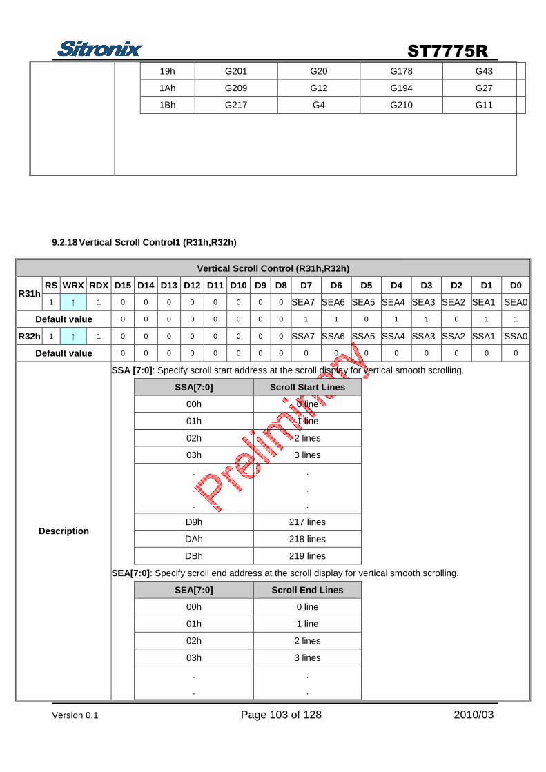
9.2.18 Vertical Scroll Control1 (R31h,R32h) ........................................................................... 103
9.2.19 Vertical Scroll Control1 (R33h) ..................................................................................... 104
9.2.20 Partial Screen Driving Position (R34h,R35h)............................................................... 105
9.2.21 Horizontal and Vertical RAM Address Position (R36h, R37h, R38h, R39h) ............. 105
9.2.22 Gamma Control (R50h~R59h) ....................................................................................... 106
Page 4
ST7775R
Version 0.1 Page 4 of 128 2010/03
9.2.23 ID Code(R65h, Read Only)............................................................................................. 108
9.2.24 SPI Read/Write Control(R66h)....................................................................................... 108
9.2.25 Power Control 2 (RB0h) ................................................................................................. 109
9.2.26 Power Control 3 (RB1h) ................................................................................................. 111
9.2.27 Power Control 4 (RB2h) ................................................................................................. 112
9.2.28 Power Control 5 (RB3h) .................................................................... 錯誤! 尚未定義書籤。
9.2.29 Power Control 6 (RB5h) .................................................................... 錯誤! 尚未定義書籤。
9.2.30 NVM ID Code (RD2h) ...................................................................................................... 113
9.2.31 NVM Control Status (RD9h)........................................................................................... 113
9.2.32 NVM Write Command (RDFh)........................................................................................ 114
9.2.33 NVM Enable (RFAh)........................................................................................................ 115
9.2.34 NVM VCOM Offset (RFEh) ............................................................................................. 115
9.2.35 NVM Command Enable (RFFh) ..................................................................................... 115
10 RESET FUNCTION ............................................................................ 116
10.1.. System Function Command List ......................................................................116
10.2.. RAM Data Initialization ....................................................................................116
10.3.. Note on Reset Function ...................................................................................116
10.4.. Reset Timing Characteristic.............................................................................116
11 8 - COLOR DISPLAY MODE.............................................................. 118
12 WINDOW ADDRESS FUNCTION ...................................................... 119
13 GAMMA CORRECTION..................................................................... 120
14 APPLICATION ................................................................................... 123
14.1.. Configuration of Power Supply Circuit .............................................................123
14.2.. Standby Mode..................................................................................................124
14.3.. Power Supply Configuration ............................................................................125
14.4.. Voltage Generation..........................................................................................126
14.5.. Applied Voltage to the TFT panel ....................................................................127
15 REVISION HISTORY.......................................................................... 128
Page 5
ST7775R
Version 0.1 Page 5 of 128 2010/03
LIST OF FIGURES Figure 1 Parallel Interface Timing Characteristics (8080-Series MCU Interface) ........................................... 38
Figure 2 Rising and Falling Timing for I/O Signal ............................................................................................ 39
Figure 3 Write-to-Read and Read-to-Write Timing.......................................................................................... 39
Figure 4 Parallel Interface Timing Characteristics (6800-Series MCU Interface) ........................................... 40
Figure 5 SPI Interface Timing Characteristics ................................................................................................. 41
Figure 6 RGB Interface Timing Characteristics ............................................................................................... 42
Figure 7 8080-Series WRX Protocol ............................................................................................................... 45
Figure 8 8080-Series Parallel Bus Protocol, Write to Register or Display RAM ............................................. 45
Figure 9 6800-Series WRX Protocol ............................................................................................................... 46
Figure 10 6800-Series Parallel Bus Protocol, Write to Register or Display RAM ........................................... 46
Figure 11 18 bits Interface Data Format (Command Write/DRAM Write) ....................................................... 47
Figure 12 16 bits Interface Data Format (Command Write/Display RAM Write)............................................. 49
Figure 13 9 bits Interface Data Format (Command Write/Display RAM Write)............................................... 50
Figure 14 8 bits interface data format (command write/Display RAM write) ................................................... 52
Figure 15 8080-Series Read Protocol ............................................................................................................. 53
Figure 16 8080-series parallel bus protocol, read data from register or display RAM .................................... 53
Figure 17 6800-Series Read Protocol ............................................................................................................. 54
Figure 18 6800-series parallel bus protocol, read data from register or display RAM .................................... 54
Figure 19 18 bits Interface Data Format (Command Read/Display RAM Read) ............................................ 55
Figure 20 16 bits Interface Data Format (Command Read/Display RAM Read) ............................................ 56
Figure 21 9 bits Interface Data Format (Command Read/Display RAM Read) .............................................. 57
Figure 22 8 bits Interface Data Format (Command Read/Display RAM Read) .............................................. 58
Figure 23 DRAM Address Map Table.............................................................................................................. 59
Figure 24 RGB Interface Data Format............................................................................................................. 60
Figure 25 DRAM Access Area by RGB Interface............................................................................................ 61
Figure 26 Timing Chart of Signals in 18-/16-bit RGB Interface Mode............................................................. 62
Figure 27 Timing chart of signals in 6-bit RGB interface mode....................................................................... 63
Figure 28 Example of update the still and moving picture............................................................................... 65
Figure 29 Example of 6-bit RGB interface data format ................................................................................... 66
Figure 30 6-bit Transfer Synchronization ........................................................................................................ 66
Figure 31 Example of 16-Bit RGB Interface and Data Format........................................................................ 67
Figure 32 Example of 18-bit RGB Interface and Data Format ........................................................................ 68
Figure 33 Internal clock operation/RGB interface mode switching ................................................................. 69
Figure 34 DRAM access between system interface and RGB interface......................................................... 70
Figure 35 Relationship between RGB I/F signals and LCD Driving Signals for Pane .................................... 71
Figure 36 Data Format of SPI Interface........................................................................................................... 73
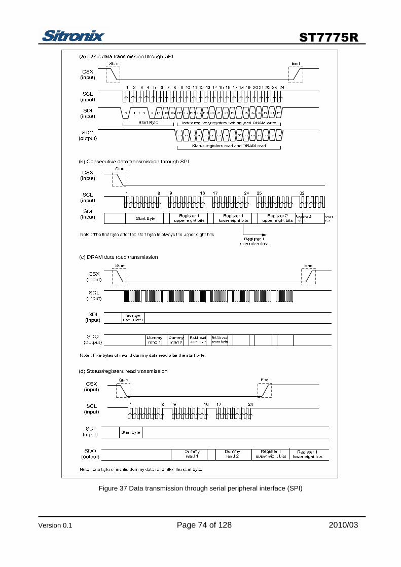
Figure 37 Data transmission through serial peripheral interface (SPI) ........................................................... 74
Page 6
ST7775R
Version 0.1 Page 6 of 128 2010/03
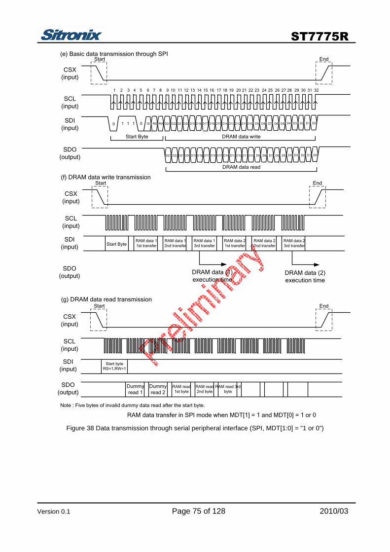
Figure 38 Data transmission through serial peripheral interface (SPI, TRI=”1” and DFM=”1 or 0”) ............... 75
Figure 39 9-bit SPI Write Register Mode......................................................................................................... 76
Figure 40 9-bit SPI Read Register mode......................................................................................................... 77
Figure 41 9-bit SPI 65K colors Serial Data Transfer, ...................................................................................... 77
Figure 42 9-bit SPI 262K colors Serial Data Transfer ..................................................................................... 78
Figure 43 8-bit SPI Write Register Mode......................................................................................................... 78
Figure 44 8-bit SPI Read Register mode......................................................................................................... 79
Figure 45 8-bit SPI 65K colors Serial Data Transfer, ...................................................................................... 79
Figure 46 8-bit SPI 262K colors Serial Data Transfer ..................................................................................... 79
Figure 47 Data Transfer Recovery .................................................................................................................. 80
Figure 48 Register Setting with Serial Peripheral Interface (SPI) ................................................................... 81
Figure 49 Register setting with i80 System Interface ...................................................................................... 82
Figure 50 Register Read/Write Timing of i80 System Interface ...................................................................... 83
Figure 51 Reset Timing ................................................................................................................................. 116
Figure 52 8-Color Display Mode.................................................................................................................... 118
Figure 53 DRAM Access Window Map ......................................................................................................... 119
Figure 54 Grayscale Voltage Generation (Positive) ...................................................................................... 120
Figure 55 Grayscale Voltage Generation (Negative) .................................................................................... 121
Figure 56 Relationship between Source Output and VCOM......................................................................... 122
Figure 57 Relationship between DRAM Data and Output Level ................................................................... 122
Figure 58 Power Supply Circuit Block ........................................................................................................... 123
Figure 59 Standby Mode Register Setting Sequence ................................................................................... 124
Figure 60 Power Supply ON/OFF Sequence ................................................................................................ 125
Figure 61 Power Booster Level ..................................................................................................................... 126
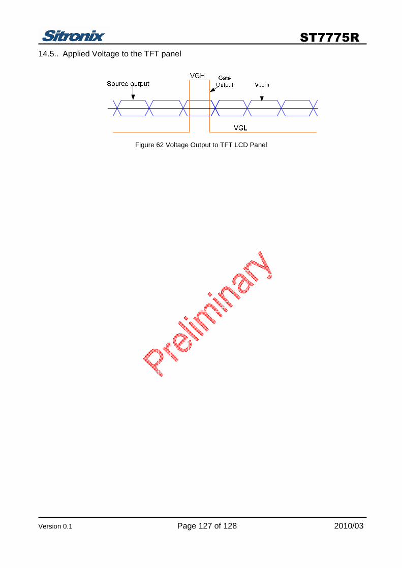
Figure 62 Voltage Output to TFT LCD Panel ................................................................................................ 127
Page 7
ST7775R
Version 0.1 Page 7 of 128 2010/03
LIST OF TABLES Table 1 Absolute Operation Range ................................................................................................................. 35
Table 2 Basic DC Characteristics.................................................................................................................... 36
Table 3 Power Consumption ........................................................................................................................... 37
Table 4 8080 Parallel Interface Characteristics............................................................................................... 39
Table 5 8080 Parallel Interface Characteristics............................................................................................... 40
Table 6 SPI Interface Characteristics .............................................................................................................. 41
Table 7 18/16 Bits RGB Interface Timing Characteristics ............................................................................... 42
Table 8 6 Bits RGB Interface Timing Characteristics ...................................................................................... 43
Table 9 Interface Type Selection..................................................................................................................... 44
Table 10 System Function Command List....................................................................................................... 85
Table 11 Reset timing Characteristics........................................................................................................... 117
Table 12 Outside Components...................................................................................................................... 123
Page 8
ST7775R
Version 0.1 Page 8 of 128 2010/03
1 GENERAL DESCRIPTION
The ST7775R is a single-chip controller/driver for 262K-color, graphic type TFT-LCD. It consists of 528
source line and 220 gate line driving circuits. This chip is capable of connecting directly to an external
microprocessor, and accepts, 8-bits/9-bits/16-bits/18-bits parallel interface. Display data can be stored in the
on-chip display data RAM of 176x220x18 bits. It can perform display data RAM read/write operation with no
external operation clock to minimize power consumption. In addition, because of the integrated power supply
circuit necessary to drive liquid crystal; it is possible to make a display system with the fewest components.
Page 9
ST7775R
Version 0.1 Page 9 of 128 2010/03
2 FEATURES
Single chip TFT-LCD Controller/Driver with On-chip Frame Memory (FM)
Display Resolution: 176*RGB (H) *220(V)
Frame Memory Size: 176 x 220 x 18-bit = 696,960 bits
LCD Driver Output Circuits
- Source Outputs: 176 RGB Channels
- Gate Outputs: 220 Channels
- Common Electrode Output
Display Colors (Color Mode)
- Full Color: 262K, RGB=(666) max., Idle Mode Off
- Color Reduce: 8-color, RGB=(111), Idle Mode On
Programmable Pixel Color Format (Color Depth) for Various Display Data input Format
- 12-bit/pixel: RGB=(444) using the 696,960 bits frame memory
- 16-bit/pixel: RGB=(565) using the 696,960 bits frame memory
- 18-bit/pixel: RGB=(666) using the 696,960 bits frame memory
MCU Interface
- Parallel 8080-series MCU Interface (8-bit, 9-bit, 16-bit & 18-bit)
- Parallel 6800-series MCU Interface (8-bit, 9-bit, 16-bit & 18-bit)
- 6/16/18 RGB Interface(VSYNC, HSYNC, DOTCLK, ENABLE, DB[17:0])
- Serial Peripheral Interface(SPI Interface)
- VSYNC Interface
Display Features
- Programmable Partial Display Duty
Support LC Type
- Support both normal-black & normal-white LC
On Chip Build-In Circuits
- DC/DC Converter
- Adjustable VCOM Generation
- Non-Volatile (NV) Memory to Store Initial Register Setting and Factory Default Value (Module ID,
Module Version, etc)
- Oscillator for Display Clock Generation
- Timing Controller
Build-In NV Memory for LCD Initial Register Setting
- 4-bits for ID2
- 5-bits for flicker adjustment
Driving Algorithm
- Dot Inversion
Page 10
ST7775R
Version 0.1 Page 10 of 128 2010/03
- Column Inversion
Wide Supply Voltage Range
- I/O Voltage (VDDI to DGND): 1.65V ~ 3.3V
- Analog Voltage (VDD to AGND): 2.5V ~ 3.3V
On-Chip Power System
- Source Voltage (GVDD to GVCL): +4.7~-4.7V
- VCOM level: -0.425V ~ -2V
- Gate driver HIGH level (VGH to AGND): +10.0V ~ +15V
- Gate driver LOW level (VGL to AGND): -13V ~ -7.5V
Optimized layout for COG Assembly
Operate temperature range: −30 to +85
Lower Power Consumption
Page 11
ST7775R
Version 0.1 Page 11 of 128 2010/03
VCCVCCVCCVCCVCCVCCVCCVCCVCCVDDI
VDDIVDDIVDDIVDDIVDDI
DUMMYDUMMYGVDDGVDDGVDD
GVDDGVCLGVCLVCLVCL
DUMMYDUMMYDUMMYDUMMYVCOM
VCOMVCOMVCOM
DUMMYDUMMY
Y
X
DUMMYDUMMYDUMMYDUMMYG1G3G5G7G9G11
G207G209G211G213G215G217G219DUMMYDUMMYDUMMYDUMMYDUMMYDUMMYDUMMYDUMMY
S253S254S255S256S257S258S259S260S261S262S263S264
S265S266S267S268S269S270S271S272S273S274S275S276
S520S521S522S523S524S525S526S527S528
G220G218G216G214
G14G12G10G8G6G4G2DUMMYDUMMYDUMMYDUMMY
DUMMYDUMMYVCOMVCOMVCOMVCOM
DUMMYVGHVGHVGH
VGHVGH
DUMMY VGLVGLVGLVGLVGL
DUMMYVPP
VPPVPP
DUMMYDUMMYDUMMYDUMMYDUMMYDUMMYDUMMYDUMMY
DUMMYDUMMYDUMMYAGNDAGNDAGNDAGNDAGNDAGNDAGND
AGNDAGNDAGND
DUMMYDUMMYDUMMYDUMMYDUMMYDUMMYDUMMY
DUMMYDUMMYDUMMYDUMMYDUMMYDUMMYDUMMYDUMMYDUMMYDUMMY
DUMMYDUMMYDUMMYDUMMYDUMMYDUMMYDUMMYDUMMYDUMMYDUMMY
DUMMYDUMMYDUMMYDUMMYDUMMYDUMMYDUMMYDUMMYDUMMYDUMMY
DUMMYDUMMYDUMMYDUMMYDUMMYDUMMYDUMMYAVDDAVDDAVDD
AVDDAVDDAVDDAVDDAVDDVDDVDDVDDVDDVDD
VDDVDDVDDVDDVDDAVCLAVCLAVCLAVCLAVCL
DUMMYDCXCSX
VSYNCHSYNCDOTCLKENABLERESET
SDIRDX
WRX_SCLDB17DB16DB15DB14DB13DB12DB11DB10DB9
DB8DB7DB6DB5DB4DB3DB2DB1DB0IM3
IM2IM1
IM0/IDSDO
DUMMYFMARKTPI0TPI1TPI2TPI3
TPO0TPO1TPO2TPO3
DUMMYOSC
AGNDAGNDAGNDAGND
AGNDAGNDAGNDAGNDAGNDDGNDDGNDDGNDDGNDDGND
DGNDDGNDDGNDDGND DGNDAGNDAGND VCC VCCVCC
S1S2S3S4S5S6S7S8S9
Bump View
DUMMYDUMMYDUMMYDUMMYDUMMYDUMMYDUMMYDUMMYDUMMY
3 PAD ARRANGEMENT
3.1.. Pad Arrangement
Au bump height 12µm
16µmx85µm
Gate : G1~G220
Source : S1~S528 Au bump size
40µmx36µm
Input Pads : Pad1 to Pad215
Page 12
ST7775R
Version 0.1 Page 12 of 128 2010/03
3.2.. Bump Dimension
output Pads
S1~S528、G1~G220、DUMMY
(No.216~988)
input Pads
I/O Pads
(No.1~215)
E F
G
H
Symbol Item Size
A Bump Width 16 um
B Bump Gap 1 (Horizontal) 16 um
C Bump Height 85 um
D Bump Gap 2 (Vertical) 68 um
Symbol Item Size
E Bump Width 40 um
F Bump Gap 20、45 um
G Bump Height 46 um
H Bump Pitch 60、85 um
Page 13
ST7775R
Version 0.1 Page 13 of 128 2010/03
3.3.. Alignment Mark Dimension
Alignment Mark: A1(X,Y)=(-6852.5,266.5)
2525 25
25
23
Alignment Mark: A2(X,Y)=(6852.5,266.5)
2525 25
25
23
3.4.. Chip Information
Chip size 14000µm x660µm
Chip thickness 300µm
Pad Location Pad center
Coordinate Origin Chip center
Page 14
ST7775R
Version 0.1 Page 14 of 128 2010/03
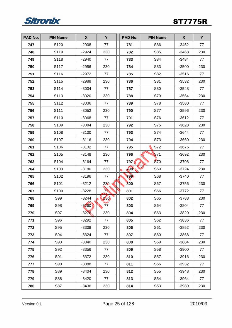
4 PAD CENTER COORDINATES
PAD No. PIN Name X Y PAD No. PIN Name X Y
1 DUMMY -6695 -251 34 AGND -4715 -251
2 DUMMY -6635 -251 35 AGND -4655 -251
3 VCOM -6575 -251 36 AGND -4595 -251
4 VCOM -6515 -251 37 AGND -4535 -251
5 VCOM -6455 -251 38 AGND -4475 -251
6 VCOM -6395 -251 39 AGND -4415 -251
7 DUMMY -6335 -251 40 AGND -4355 -251
8 VGH -6275 -251 41 AGND -4295 -251
9 VGH -6215 -251 42 AGND -4235 -251
10 VGH -6155 -251 43 AGND -4175 -251
11 VGH -6095 -251 44 DUMMY -4115 -251
12 VGH -6035 -251 45 DUMMY -4055 -251
13 DUMMY -5975 -251 46 DUMMY -3995 -251
14 VGL -5915 -251 47 DUMMY -3935 -251
15 VGL -5855 -251 48 DUMMY -3875 -251
16 VGL -5795 -251 49 DUMMY -3815 -251
17 VGL -5735 -251 50 DUMMY -3755 -251
18 VGL -5675 -251 51 DUMMY -3695 -251
19 DUMMY -5615 -251 52 DUMMY -3635 -251
20 VPP -5555 -251 53 DUMMY -3575 -251
21 VPP -5495 -251 54 DUMMY -3515 -251
22 VPP -5435 -251 55 DUMMY -3455 -251
23 DUMMY -5375 -251 56 DUMMY -3395 -251
24 DUMMY -5315 -251 57 DUMMY -3335 -251
25 DUMMY -5255 -251 58 DUMMY -3275 -251
26 DUMMY -5195 -251 59 DUMMY -3215 -251
27 DUMMY -5135 -251 60 DUMMY -3155 -251
28 DUMMY -5075 -251 61 DUMMY -3095 -251
29 DUMMY -5015 -251 62 DUMMY -3035 -251
30 DUMMY -4955 -251 63 DUMMY -2975 -251
31 DUMMY -4895 -251 64 DUMMY -2915 -251
32 DUMMY -4835 -251 65 DUMMY -2855 -251
33 DUMMY -4775 -251 66 DUMMY -2795 -251
Page 15
ST7775R
Version 0.1 Page 15 of 128 2010/03
PAD No. PIN Name X Y PAD No. PIN Name X Y
67 DUMMY -2735 -251 101 VDD -695 -251
68 DUMMY -2675 -251 102 VDD -635 -251
69 DUMMY -2615 -251 103 VDD -575 -251
70 DUMMY -2555 -251 104 VDD -515 -251
71 DUMMY -2495 -251 105 VDD -455 -251
72 DUMMY -2435 -251 106 AVCL -395 -251
73 DUMMY -2375 -251 107 AVCL -335 -251
74 DUMMY -2315 -251 108 AVCL -275 -251
75 DUMMY -2255 -251 109 AVCL -215 -251
76 DUMMY -2195 -251 110 AVCL -155 -251
77 DUMMY -2135 -251 111 DUMMY -95 -251
78 DUMMY -2075 -251 112 DCX(RS) -35 -251
79 DUMMY -2015 -251 113 CSX 25 -251
80 DUMMY -1955 -251 114 VSYNC 85 -251
81 DUMMY -1895 -251 115 HSYNC 145 -251
82 DUMMY -1835 -251 116 DOTCLK 205 -251
83 DUMMY -1775 -251 117 ENABLE 265 -251
84 DUMMY -1715 -251 118 RESET 325 -251
85 DUMMY -1655 -251 119 SDI(SDA) 385 -251
86 DUMMY -1595 -251 120 RDX 445 -251
87 DUMMY -1535 -251 121 WRX(SCL) 505 -251
88 AVDD -1475 -251 122 DB17 565 -251
89 AVDD -1415 -251 123 DB16 650 -251
90 AVDD -1355 -251 124 DB15 735 -251
91 AVDD -1295 -251 125 DB14 820 -251
92 AVDD -1235 -251 126 DB13 905 -251
93 AVDD -1175 -251 127 DB12 990 -251
94 AVDD -1115 -251 128 DB11 1075 -251
95 AVDD -1055 -251 129 DB10 1160 -251
96 VDD -995 -251 130 DB9 1245 -251
97 VDD -935 -251 131 DB8 1330 -251
98 VDD -875 -251 132 DB7 1415 -251
99 VDD -815 -251 133 DB6 1500 -251
100 VDD -755 -251 134 DB5 1585 -251
Page 16
ST7775R
Version 0.1 Page 16 of 128 2010/03
PAD No. PIN Name X Y PAD No. PIN Name X Y
135 DB4 1670 -251 169 DGND 3935 -251
136 DB3 1755 -251 170 DGND 3995 -251
137 DB2 1840 -251 171 DGND 4055 -251
138 DB1 1925 -251 172 DGND 4115 -251
139 DB0 2010 -251 173 DGND 4175 -251
140 IM3 2095 -251 174 DGND 4235 -251
141 IM2 2155 -251 175 DGND 4295 -251
142 IM1 2215 -251 176 AGND 4355 -251
143 IM0_ID 2275 -251 177 AGND 4415 -251
144 SDO 2335 -251 178 VCC 4475 -251
145 DUMMY 2420 -251 179 VCC 4535 -251
146 FMARK 2505 -251 180 VCC 4595 -251
147 TPI0 2590 -251 181 VCC 4655 -251
148 TPI1 2675 -251 182 VCC 4715 -251
149 TPI2 2735 -251 183 VCC 4775 -251
150 TPI3 2795 -251 184 VCC 4835 -251
151 TPO0 2855 -251 185 VCC 4895 -251
152 TPO1 2915 -251 186 VCC 4955 -251
153 TPO2 2975 -251 187 VCC 5015 -251
154 TPO3 3035 -251 188 VCC 5075 -251
155 DUMMY 3095 -251 189 VCC 5135 -251
156 OSC 3155 -251 190 VDDI 5195 -251
157 AGND 3215 -251 191 VDDI 5255 -251
158 AGND 3275 -251 192 VDDI 5315 -251
159 AGND 3335 -251 193 VDDI 5375 -251
160 AGND 3395 -251 194 VDDI 5435 -251
161 AGND 3455 -251 195 VDDI 5495 -251
162 AGND 3515 -251 196 DUMMY 5555 -251
163 AGND 3575 -251 197 DUMMY 5615 -251
164 AGND 3635 -251 198 GVDD 5675 -251
165 AGND 3695 -251 199 GVDD 5735 -251
166 DGND 3755 -251 200 GVDD 5795 -251
167 DGND 3815 -251 201 GVDD 5855 -251
168 DGND 3875 -251 202 GVCL 5915 -251
Page 17
ST7775R
Version 0.1 Page 17 of 128 2010/03
PAD No. PIN Name X Y PAD No. PIN Name X Y
203 GVCL 5975 -251 237 G36 6436 77
204 VCL 6035 -251 238 G38 6420 230
205 VCL 6095 -251 239 G40 6404 77
206 DUMMY 6155 -251 240 G42 6388 230
207 DUMMY 6215 -251 241 G44 6372 77
208 DUMMY 6275 -251 242 G46 6356 230
209 DUMMY 6335 -251 243 G48 6340 77
210 VCOM 6395 -251 244 G50 6324 230
211 VCOM 6455 -251 245 G52 6308 77
212 VCOM 6515 -251 246 G54 6292 230
213 VCOM 6575 -251 247 G56 6276 77
214 DUMMY 6635 -251 248 G58 6260 230
215 DUMMY 6695 -251 249 G60 6244 77
216 DUMMY 6772 230 250 G62 6228 230
217 DUMMY 6756 77 251 G64 6212 77
218 DUMMY 6740 230 252 G66 6196 230
219 DUMMY 6724 77 253 G68 6180 77
220 G2 6708 230 254 G70 6164 230
221 G4 6692 77 255 G72 6148 77
222 G6 6676 230 256 G74 6132 230
223 G8 6660 77 257 G76 6116 77
224 G10 6644 230 258 G78 6100 230
225 G12 6628 77 259 G80 6084 77
226 G14 6612 230 260 G82 6068 230
227 G16 6596 77 261 G84 6052 77
228 G18 6580 230 262 G86 6036 230
229 G20 6564 77 263 G88 6020 77
230 G22 6548 230 264 G90 6004 230
231 G24 6532 77 265 G92 5988 77
232 G26 6516 230 266 G94 5972 230
233 G28 6500 77 267 G96 5956 77
234 G30 6484 230 268 G98 5940 230
235 G32 6468 77 269 G100 5924 77
236 G34 6452 230 270 G102 5908 230
Page 18
ST7775R
Version 0.1 Page 18 of 128 2010/03
PAD No. PIN Name X Y PAD No. PIN Name X Y
271 G104 5892 77 305 G172 5348 77
272 G106 5876 230 306 G174 5332 230
273 G108 5860 77 307 G176 5316 77
274 G110 5844 230 308 G178 5300 230
275 G112 5828 77 309 G180 5284 77
276 G114 5812 230 310 G182 5268 230
277 G116 5796 77 311 G184 5252 77
278 G118 5780 230 312 G186 5236 230
279 G120 5764 77 313 G188 5220 77
280 G122 5748 230 314 G190 5204 230
281 G124 5732 77 315 G192 5188 77
282 G126 5716 230 316 G194 5172 230
283 G128 5700 77 317 G196 5156 77
284 G130 5684 230 318 G198 5140 230
285 G132 5668 77 319 G200 5124 77
286 G134 5652 230 320 G202 5108 230
287 G136 5636 77 321 G204 5092 77
288 G138 5620 230 322 G206 5076 230
289 G140 5604 77 323 G208 5060 77
290 G142 5588 230 324 G210 5044 230
291 G144 5572 77 325 G212 5028 77
292 G146 5556 230 326 G214 5012 230
293 G148 5540 77 327 G216 4996 77
294 G150 5524 230 328 G218 4980 230
295 G152 5508 77 329 G220 4964 77
296 G154 5492 230 330 DUMMY 4948 230
297 G156 5476 77 331 DUMMY 4932 77
298 G158 5460 230 332 DUMMY 4916 230
299 G160 5444 77 333 DUMMY 4900 77
300 G162 5428 230 334 DUMMY 4884 230
301 G164 5412 77 335 DUMMY 4868 77
302 G166 5396 230 336 DUMMY 4852 230
303 G168 5380 77 337 DUMMY 4836 77
304 G170 5364 230 338 DUMMY 4820 230
Page 19
ST7775R
Version 0.1 Page 19 of 128 2010/03
PAD No. PIN Name X Y PAD No. PIN Name X Y
339 S528 4804 77 373 S494 4260 77
340 S527 4788 230 374 S493 4244 230
341 S526 4772 77 375 S492 4228 77
342 S525 4756 230 376 S491 4212 230
343 S524 4740 77 377 S490 4196 77
344 S523 4724 230 378 S489 4180 230
345 S522 4708 77 379 S488 4164 77
346 S521 4692 230 380 S487 4148 230
347 S520 4676 77 381 S486 4132 77
348 S519 4660 230 382 S485 4116 230
349 S518 4644 77 383 S484 4100 77
350 S517 4628 230 384 S483 4084 230
351 S516 4612 77 385 S482 4068 77
352 S515 4596 230 386 S481 4052 230
353 S514 4580 77 387 S480 4036 77
354 S513 4564 230 388 S479 4020 230
355 S512 4548 77 389 S478 4004 77
356 S511 4532 230 390 S477 3988 230
357 S510 4516 77 391 S476 3972 77
358 S509 4500 230 392 S475 3956 230
359 S508 4484 77 393 S474 3940 77
360 S507 4468 230 394 S473 3924 230
361 S506 4452 77 395 S472 3908 77
362 S505 4436 230 396 S471 3892 230
363 S504 4420 77 397 S470 3876 77
364 S503 4404 230 398 S469 3860 230
365 S502 4388 77 399 S468 3844 77
366 S501 4372 230 400 S467 3828 230
367 S500 4356 77 401 S466 3812 77
368 S499 4340 230 402 S465 3796 230
369 S498 4324 77 403 S464 3780 77
370 S497 4308 230 404 S463 3764 230
371 S496 4292 77 405 S462 3748 77
372 S495 4276 230 406 S461 3732 230
Page 20
ST7775R
Version 0.1 Page 20 of 128 2010/03
PAD No. PIN Name X Y PAD No. PIN Name X Y
407 S460 3716 77 441 S426 3172 77
408 S459 3700 230 442 S425 3156 230
409 S458 3684 77 443 S424 3140 77
410 S457 3668 230 444 S423 3124 230
411 S456 3652 77 445 S422 3108 77
412 S455 3636 230 446 S421 3092 230
413 S454 3620 77 447 S420 3076 77
414 S453 3604 230 448 S419 3060 230
415 S452 3588 77 449 S418 3044 77
416 S451 3572 230 450 S417 3028 230
417 S450 3556 77 451 S416 3012 77
418 S449 3540 230 452 S415 2996 230
419 S448 3524 77 453 S414 2980 77
420 S447 3508 230 454 S413 2964 230
421 S446 3492 77 455 S412 2948 77
422 S445 3476 230 456 S411 2932 230
423 S444 3460 77 457 S410 2916 77
424 S443 3444 230 458 S409 2900 230
425 S442 3428 77 459 S408 2884 77
426 S441 3412 230 460 S407 2868 230
427 S440 3396 77 461 S406 2852 77
428 S439 3380 230 462 S405 2836 230
429 S438 3364 77 463 S404 2820 77
430 S437 3348 230 464 S403 2804 230
431 S436 3332 77 465 S402 2788 77
432 S435 3316 230 466 S401 2772 230
433 S434 3300 77 467 S400 2756 77
434 S433 3284 230 468 S399 2740 230
435 S432 3268 77 469 S398 2724 77
436 S431 3252 230 470 S397 2708 230
437 S430 3236 77 471 S396 2642 77
438 S429 3220 230 472 S395 2626 230
439 S428 3204 77 473 S394 2610 77
440 S427 3188 230 474 S393 2594 230
Page 21
ST7775R
Version 0.1 Page 21 of 128 2010/03
PAD No. PIN Name X Y PAD No. PIN Name X Y
475 S392 2578 77 509 S358 2034 77
476 S391 2562 230 510 S357 2018 230
477 S390 2546 77 511 S356 2002 77
478 S389 2530 230 512 S355 1986 230
479 S388 2514 77 513 S354 1970 77
480 S387 2498 230 514 S353 1954 230
481 S386 2482 77 515 S352 1938 77
482 S385 2466 230 516 S351 1922 230
483 S384 2450 77 517 S350 1906 77
484 S383 2434 230 518 S349 1890 230
485 S382 2418 77 519 S348 1874 77
486 S381 2402 230 520 S347 1858 230
487 S380 2386 77 521 S346 1842 77
488 S379 2370 230 522 S345 1826 230
489 S378 2354 77 523 S344 1810 77
490 S377 2338 230 524 S343 1794 230
491 S376 2322 77 525 S342 1778 77
492 S375 2306 230 526 S341 1762 230
493 S374 2290 77 527 S340 1746 77
494 S373 2274 230 528 S339 1730 230
495 S372 2258 77 529 S338 1714 77
496 S371 2242 230 530 S337 1698 230
497 S370 2226 77 531 S336 1682 77
498 S369 2210 230 532 S335 1666 230
499 S368 2194 77 533 S334 1650 77
500 S367 2178 230 534 S333 1634 230
501 S366 2162 77 535 S332 1618 77
502 S365 2146 230 536 S331 1602 230
503 S364 2130 77 537 S330 1586 77
504 S363 2114 230 538 S329 1570 230
505 S362 2098 77 539 S328 1554 77
506 S361 2082 230 540 S327 1538 230
507 S360 2066 77 541 S326 1522 77
508 S359 2050 230 542 S325 1506 230
Page 22
ST7775R
Version 0.1 Page 22 of 128 2010/03
PAD No. PIN Name X Y PAD No. PIN Name X Y
543 S324 1490 77 577 S290 946 77
544 S323 1474 230 578 S289 930 230
545 S322 1458 77 579 S288 914 77
546 S321 1442 230 580 S287 898 230
547 S320 1426 77 581 S286 882 77
548 S319 1410 230 582 S285 866 230
549 S318 1394 77 583 S284 850 77
550 S317 1378 230 584 S283 834 230
551 S316 1362 77 585 S282 818 77
552 S315 1346 230 586 S281 802 230
553 S314 1330 77 587 S280 786 77
554 S313 1314 230 588 S279 770 230
555 S312 1298 77 589 S278 754 77
556 S311 1282 230 590 S277 738 230
557 S310 1266 77 591 S276 722 77
558 S309 1250 230 592 S275 706 230
559 S308 1234 77 593 S274 690 77
560 S307 1218 230 594 S273 674 230
561 S306 1202 77 595 S272 658 77
562 S305 1186 230 596 S271 642 230
563 S304 1170 77 597 S270 626 77
564 S303 1154 230 598 S269 610 230
565 S302 1138 77 599 S268 594 77
566 S301 1122 230 600 S267 578 230
567 S300 1106 77 601 S266 562 77
568 S299 1090 230 602 S265 546 230
569 S298 1074 77 603 S264 -554 77
570 S297 1058 230 604 S263 -570 230
571 S296 1042 77 605 S262 -586 77
572 S295 1026 230 606 S261 -602 230
573 S294 1010 77 607 S260 -618 77
574 S293 994 230 608 S259 -634 230
575 S292 978 77 609 S258 -650 77
576 S291 962 230 610 S257 -666 230
Page 23
ST7775R
Version 0.1 Page 23 of 128 2010/03
PAD No. PIN Name X Y PAD No. PIN Name X Y
611 S256 -682 77 645 S222 -1226 77
612 S255 -698 230 646 S221 -1242 230
613 S254 -714 77 647 S220 -1258 77
614 S253 -730 230 648 S219 -1274 230
615 S252 -746 77 649 S218 -1290 77
616 S251 -762 230 650 S217 -1306 230
617 S250 -778 77 651 S216 -1322 77
618 S249 -794 230 652 S215 -1338 230
619 S248 -810 77 653 S214 -1354 77
620 S247 -826 230 654 S213 -1370 230
621 S246 -842 77 655 S212 -1386 77
622 S245 -858 230 656 S211 -1402 230
623 S244 -874 77 657 S210 -1418 77
624 S243 -890 230 658 S209 -1434 230
625 S242 -906 77 659 S208 -1450 77
626 S241 -922 230 660 S207 -1466 230
627 S240 -938 77 661 S206 -1482 77
628 S239 -954 230 662 S205 -1498 230
629 S238 -970 77 663 S204 -1514 77
630 S237 -986 230 664 S203 -1530 230
631 S236 -1002 77 665 S202 -1546 77
632 S235 -1018 230 666 S201 -1562 230
633 S234 -1034 77 667 S200 -1578 77
634 S233 -1050 230 668 S199 -1594 230
635 S232 -1066 77 669 S198 -1610 77
636 S231 -1082 230 670 S197 -1626 230
637 S230 -1098 77 671 S196 -1642 77
638 S229 -1114 230 672 S195 -1658 230
639 S228 -1130 77 673 S194 -1674 77
640 S227 -1146 230 674 S193 -1690 230
641 S226 -1162 77 675 S192 -1706 77
642 S225 -1178 230 676 S191 -1722 230
643 S224 -1194 77 677 S190 -1738 77
644 S223 -1210 230 678 S189 -1754 230
Page 24
ST7775R
Version 0.1 Page 24 of 128 2010/03
PAD No. PIN Name X Y PAD No. PIN Name X Y
679 S188 -1770 77 713 S154 -2314 77
680 S187 -1786 230 714 S153 -2330 230
681 S186 -1802 77 715 S152 -2346 77
682 S185 -1818 230 716 S151 -2362 230
683 S184 -1834 77 717 S150 -2378 77
684 S183 -1850 230 718 S149 -2394 230
685 S182 -1866 77 719 S148 -2410 77
686 S181 -1882 230 720 S147 -2426 230
687 S180 -1898 77 721 S146 -2442 77
688 S179 -1914 230 722 S145 -2458 230
689 S178 -1930 77 723 S144 -2474 77
690 S177 -1946 230 724 S143 -2490 230
691 S176 -1962 77 725 S142 -2506 77
692 S175 -1978 230 726 S141 -2522 230
693 S174 -1994 77 727 S140 -2538 77
694 S173 -2010 230 728 S139 -2554 230
695 S172 -2026 77 729 S138 -2570 77
696 S171 -2042 230 730 S137 -2586 230
697 S170 -2058 77 731 S136 -2602 77
698 S169 -2074 230 732 S135 -2618 230
699 S168 -2090 77 733 S134 -2634 77
700 S167 -2106 230 734 S133 -2650 230
701 S166 -2122 77 735 S132 -2716 77
702 S165 -2138 230 736 S131 -2732 230
703 S164 -2154 77 737 S130 -2748 77
704 S163 -2170 230 738 S129 -2764 230
705 S162 -2186 77 739 S128 -2780 77
706 S161 -2202 230 740 S127 -2796 230
707 S160 -2218 77 741 S126 -2812 77
708 S159 -2234 230 742 S125 -2828 230
709 S158 -2250 77 743 S124 -2844 77
710 S157 -2266 230 744 S123 -2860 230
711 S156 -2282 77 745 S122 -2876 77
712 S155 -2298 230 746 S121 -2892 230
Page 25
ST7775R
Version 0.1 Page 25 of 128 2010/03
PAD No. PIN Name X Y PAD No. PIN Name X Y
747 S120 -2908 77 781 S86 -3452 77
748 S119 -2924 230 782 S85 -3468 230
749 S118 -2940 77 783 S84 -3484 77
750 S117 -2956 230 784 S83 -3500 230
751 S116 -2972 77 785 S82 -3516 77
752 S115 -2988 230 786 S81 -3532 230
753 S114 -3004 77 787 S80 -3548 77
754 S113 -3020 230 788 S79 -3564 230
755 S112 -3036 77 789 S78 -3580 77
756 S111 -3052 230 790 S77 -3596 230
757 S110 -3068 77 791 S76 -3612 77
758 S109 -3084 230 792 S75 -3628 230
759 S108 -3100 77 793 S74 -3644 77
760 S107 -3116 230 794 S73 -3660 230
761 S106 -3132 77 795 S72 -3676 77
762 S105 -3148 230 796 S71 -3692 230
763 S104 -3164 77 797 S70 -3708 77
764 S103 -3180 230 798 S69 -3724 230
765 S102 -3196 77 799 S68 -3740 77
766 S101 -3212 230 800 S67 -3756 230
767 S100 -3228 77 801 S66 -3772 77
768 S99 -3244 230 802 S65 -3788 230
769 S98 -3260 77 803 S64 -3804 77
770 S97 -3276 230 804 S63 -3820 230
771 S96 -3292 77 805 S62 -3836 77
772 S95 -3308 230 806 S61 -3852 230
773 S94 -3324 77 807 S60 -3868 77
774 S93 -3340 230 808 S59 -3884 230
775 S92 -3356 77 809 S58 -3900 77
776 S91 -3372 230 810 S57 -3916 230
777 S90 -3388 77 811 S56 -3932 77
778 S89 -3404 230 812 S55 -3948 230
779 S88 -3420 77 813 S54 -3964 77
780 S87 -3436 230 814 S53 -3980 230
Page 26
ST7775R
Version 0.1 Page 26 of 128 2010/03
PAD No. PIN Name X Y PAD No. PIN Name X Y
815 S52 -3996 77 849 S18 -4540 77
816 S51 -4012 230 850 S17 -4556 230
817 S50 -4028 77 851 S16 -4572 77
818 S49 -4044 230 852 S15 -4588 230
819 S48 -4060 77 853 S14 -4604 77
820 S47 -4076 230 854 S13 -4620 230
821 S46 -4092 77 855 S12 -4636 77
822 S45 -4108 230 856 S11 -4652 230
823 S44 -4124 77 857 S10 -4668 77
824 S43 -4140 230 858 S9 -4684 230
825 S42 -4156 77 859 S8 -4700 77
826 S41 -4172 230 860 S7 -4716 230
827 S40 -4188 77 861 S6 -4732 77
828 S39 -4204 230 862 S5 -4748 230
829 S38 -4220 77 863 S4 -4764 77
830 S37 -4236 230 864 S3 -4780 230
831 S36 -4252 77 865 S2 -4796 77
832 S35 -4268 230 866 S1 -4812 230
833 S34 -4284 77 867 DUMMY -4828 77
834 S33 -4300 230 868 DUMMY -4844 230
835 S32 -4316 77 869 DUMMY -4860 77
836 S31 -4332 230 870 DUMMY -4876 230
837 S30 -4348 77 871 DUMMY -4892 77
838 S29 -4364 230 872 DUMMY -4908 230
839 S28 -4380 77 873 DUMMY -4924 77
840 S27 -4396 230 874 DUMMY -4940 230
841 S26 -4412 77 875 G219 -4956 77
842 S25 -4428 230 876 G217 -4972 230
843 S24 -4444 77 877 G215 -4988 77
844 S23 -4460 230 878 G213 -5004 230
845 S22 -4476 77 879 G211 -5020 77
846 S21 -4492 230 880 G209 -5036 230
847 S20 -4508 77 881 G207 -5052 77
848 S19 -4524 230 882 G205 -5068 230
Page 27
ST7775R
Version 0.1 Page 27 of 128 2010/03
PAD No. PIN Name X Y PAD No. PIN Name X Y
883 G203 -5084 77 917 G135 -5628 77
884 G201 -5100 230 918 G133 -5644 230
885 G199 -5116 77 919 G131 -5660 77
886 G197 -5132 230 920 G129 -5676 230
887 G195 -5148 77 921 G127 -5692 77
888 G193 -5164 230 922 G125 -5708 230
889 G191 -5180 77 923 G123 -5724 77
890 G189 -5196 230 924 G121 -5740 230
891 G187 -5212 77 925 G119 -5756 77
892 G185 -5228 230 926 G117 -5772 230
893 G183 -5244 77 927 G115 -5788 77
894 G181 -5260 230 928 G113 -5804 230
895 G179 -5276 77 929 G111 -5820 77
896 G177 -5292 230 930 G109 -5836 230
897 G175 -5308 77 931 G107 -5852 77
898 G173 -5324 230 932 G105 -5868 230
899 G171 -5340 77 933 G103 -5884 77
900 G169 -5356 230 934 G101 -5900 230
901 G167 -5372 77 935 G99 -5916 77
902 G165 -5388 230 936 G97 -5932 230
903 G163 -5404 77 937 G95 -5948 77
904 G161 -5420 230 938 G93 -5964 230
905 G159 -5436 77 939 G91 -5980 77
906 G157 -5452 230 940 G89 -5996 230
907 G155 -5468 77 941 G87 -6012 77
908 G153 -5484 230 942 G85 -6028 230
909 G151 -5500 77 943 G83 -6044 77
910 G149 -5516 230 944 G81 -6060 230
911 G147 -5532 77 945 G79 -6076 77
912 G145 -5548 230 946 G77 -6092 230
913 G143 -5564 77 947 G75 -6108 77
914 G141 -5580 230 948 G73 -6124 230
915 G139 -5596 77 949 G71 -6140 77
916 G137 -5612 230 950 G69 -6156 230
Page 28
ST7775R
Version 0.1 Page 28 of 128 2010/03
PAD No. PIN Name X Y PAD No. PIN Name X Y
951 G67 -6172 77 985 DUMMY -6716 77
952 G65 -6188 230 986 DUMMY -6732 230
953 G63 -6204 77 987 DUMMY -6748 77
954 G61 -6220 230 988 DUMMY -6764 230
955 G59 -6236 77
956 G57 -6252 230
957 G55 -6268 77
958 G53 -6284 230
959 G51 -6300 77
960 G49 -6316 230
961 G47 -6332 77
962 G45 -6348 230
963 G43 -6364 77
964 G41 -6380 230
965 G39 -6396 77
966 G37 -6412 230
967 G35 -6428 77
968 G33 -6444 230
969 G31 -6460 77
970 G29 -6476 230
971 G27 -6492 77
972 G25 -6508 230
973 G23 -6524 77
974 G21 -6540 230
975 G19 -6556 77
976 G17 -6572 230
977 G15 -6588 77
978 G13 -6604 230
979 G11 -6620 77
980 G9 -6636 230
981 G7 -6652 77
982 G5 -6668 230
983 G3 -6684 77
984 G1 -6700 230
Page 29
ST7775R
Version 0.1 Page 29 of 128 2010/03
5 BLOCK DIAGRAM
176 Source Buffer
DAC
Level Shifter
Data Latch
Display Ram176x 220x 18bits
Voltage Reference
Gamma Circuit
Gamma Table
Display Control
220 Gate Buffer
Level Shifter
Gate Decoder
Vcom Generator
OSC
Booster
Instruction Register
NVM
Interface
SDO
SDI
RDX
WRX/SCL
CSX
DCX/RS
IM[3:0]
RESET
DB[17:0]
AVDD
VDDI
VDD
GVDD
VCOM
GVCL
AVCL
VGH
VGL
VCL
DOTCLK
ENABLE
VSYNC
HSYNC
Page 30
ST7775R
Version 0.1 Page 30 of 128 2010/03
6 PIN DESCRIPTION
6.1.. Power Supply Pins
Name I/O Description Connect Pin
VDD I Power Supply for Analog, Digital System and Booster Circuit. VDD
VDDI I Power Supply for I/O System. VDDI
AGND I System Ground for Analog System and Booster Circuit. GND
DGND I System Ground for I/O System and Digital System. GND
Page 31
ST7775R
Version 0.1 Page 31 of 128 2010/03
6.2.. Interface Logic Pins
Name I/O Description Connect Pin
IM3, IM2,
IM1, IM0/ID I
-The MCU interface mode select.
IM3 IM2 IM1 IM0 MCU Interface Mode Data pin
0 0 0 0 68-16 bit DB[17:10], DB[8:1]
0 0 0 1 68-8 bit DB[17:10]
0 0 1 0 80-16 bit DB[17:10], DB[8:1]
0 0 1 1 80-8 bit DB[17:10],
0 1 0 ID 24-bit SPI CSX ,SCL ,SDI, SDO
0 1 1 0 9- bit SPI CSX,SCL,SDA
0 1 1 1 8- bit SPI CSX,SCL,SDA,DCX
1 0 0 0 68-18 bit DB[17:0]
1 0 0 1 68-9 bit DB[17:9]
1 0 1 0 80-18bit DB[17:0]
1 0 1 1 80-9bit DB[17:9]
1 1 -- -- Setting invalid
-When the SPI interface is selected, IM0 pin will be used for the ID
setting.
DGND/VDDI
RESET I
-This signal will reset the device and it must be applied to properly
initialize the chip.
-Signal is active low.
MCU
CSX I
-Chip selection pin
Low enable.
High disable.
MCU
DCX
(RS) I
-Display data/command selection pin in MCU interface.
DCX=’1’: display data or parameter.
DCX=’0’: command data.
-If not used, please fix this pin at VDDI or DGND level.
MCU
RDX I -Read enable in 8080 MCU parallel interface.
-If not used, please fix this pin at VDDI or DGND level. MCU
WRX
(SCL) I
-Write enable in MCU parallel interface.
In SPI mode, this is used as SCL.
-If not used, please fix this pin at VDDI or DGND level.
MCU
VSYNC I
-Vertical (Frame) synchronizing input signal for RGB interface operation.
VSPL = “0”: Active low.
VSPL = “1”: Active high.
-Fix to the GND level when not in use.
MCU
Page 32
ST7775R
Version 0.1 Page 32 of 128 2010/03
Name I/O Description Connect Pin
HSYNC I
-Horizontal (Line) synchronizing input signal for RGB interface operation.
HSPL = “0”: Active low, HSPL = “1”: Active high.
-Fix to the GND level when not in use
MCU
ENABLE I
-Data enable signal for RGB interface operation.
Low: Select (access enabled), High: Not select (access disabled)
The EPL bit inverts the polarity of the ENABLE signal.
-If not used, please fix this pin at VDDI or DGND level.
MCU
DOTCLK I
-Dot clock signal for RGB interface operation.
DPL = “0”: Input data on the rising edge of DOTCLK
DPL = “1”: Input data on the falling edge of DOTCLK
-If not used, please fix this pin at DGND level.
MCU
SDI
(SDA) I
-SPI interface input pin.
-The data is latched on the rising edge of the SCL signal.
-In the 24-bit serial peripheral interface, this pin is used as input Pin.
-In the 8/9-bit serial peripheral interface, this pin is used as bi-directional
data pin.
-If not used, please fix this pin at DGND level.
MCU
SDO I
-SPI interface output pin.
-The data is outputted on the falling edge of the SCL signal.
If not used, please fix this pin at floating.
MCU
DB[17:0] I/O
-DB[17:0] are used as MCU parallel interface data bus.
8-bit I/F: DB[17:10] is used.
9-bit I/F: DB[17:9] is used.
16-bit I/F: DB[17:10] and DB[8:1] is used.
18-bit I/F: DB[17:0] is used.
-DB[17:0] are used as RGB interface data bus.
6-bit RGB I/F: DB[17:12] are used.
16-bit RGB I/F: DB[17:13] and DB[11:1] are used.
18-bit RGB I/F: DB[17:0] are used.
-If not used, please fix this pin at VDDI or DGND level.
MCU
FMARK O
-Output frame head pulse signal is used as synchronies MCU to frame
rate
-If not used, Let this pin open
MCU
Note1. “1” = VDDI level, “0” = DGND level.
Note2. When in parallel mode, unused data pins must be connected to “1” or “0”.
Note3. When CSX=”1”, there is no influence to the parallel and serial interface.
Page 33
ST7775R
Version 0.1 Page 33 of 128 2010/03
6.3.. Driver Output Pins
Name I/O Description Connect pin
S1 to S528 O
-Source driver output pins
-To change the shift direction of signal outputs, use the SS bit.
SS = “0”, the data in the RAM address “h00000” is output from S1.
SS = “1”, the data in the RAM address “h00000” is output from S528.
-When SS=”0”
S1, S4, S7, … display red (R), S2, S5, S8, ... display green (G), and S3,
S6, S9 ... display blue (B)
LCD
G1 to G220 O
-Gate driver output pins.
VGH: Selecting Gate Lines Level.
VGL: Non-selecting Gate Lines Level.
LCD
AVDD O -Power pad for analogy circuit.
-Connect a capacitor for stabilization. Capacitor
GVDD O
- A power output of grayscale voltage generator.
- When internal GVDD generator is not used, connect an external power
supply (AVDD-0.5V) to this pin.
-
AVCL O - A power supply pin for generating GVCL.
- Connect a capacitor for stabilization. Capacitor
GVCL O
- A power output (Negative) of grayscale voltage generator.
- When internal GVCL generator is not used, connect an external power
supply (AVCL+0.5V) to this pin.
-
VCL O - A power output of VCOM voltage (Negative) generator. -
VGH O - Power output pin for gate driver -
VGL O - Power output (Negative) pin for gate driver -
VCC O - Monitoring pin of internal digital reference voltage. -
VCOM O -A power supply for the TFT-LCD common electrode. Common
Electrode
Page 34
ST7775R
Version 0.1 Page 34 of 128 2010/03
6.4.. Test Pins
Name I/O Description Connect pin
TPI0 I -These test pins for Driver vender test used. Leave this pin open Open
TPI1
TPI2
TPI3
I -This pin is for testing.
-In normal operation, connect this pin to DGND or VDDI DGND/VDDI
TPO0
TPO1
TPO2
O -These test pins for Driver vender test used.
-Please open these pins. Open
TPO3 O -This pin is for testing
-In normal operation, connect this pin to DGND or VDDI DGND/VDDI
OSC O -This pin is for testing.
- In normal operation, connect this pin to DGND or VDDI. DGND/VDDI
Dummy -
-These pins are dummy (have no function inside).
-Can allow signal traces pass through these pads on TFT glass.
-Please open these pins.
Open
Page 35
ST7775R
Version 0.1 Page 35 of 128 2010/03
7 DRIVER ELECTRICAL CHARACTERISTICS
7.1.. Absolute Operation Range
Item Symbol Rating Unit
Supply Voltage VDD - 0.3 ~ +4.6 V
Supply Voltage (Logic) VDDI - 0.3 ~ +4.6 V
Supply Voltage (Digital) VCC - 0.3 ~ +4.6 V
Driver Supply Voltage VGH-VGL - 0.3 ~ +30.0 V
Logic Input Voltage Range VIN - 0.5 ~ VDDI + 0.5 V
Logic Output Voltage Range VO - 0.5 ~ VDDI + 0.5 V
Operating Temperature Range TOPR -30 ~ +85
Storage Temperature Range TSTG -40 ~ +125
Table 1 Absolute Operation Range
Note: If one of the above items is exceeded its maximum limitation momentarily, the quality of the product may be degraded. Absolute
maximum limitation, therefore, specify the values exceeding which the product may be physically damaged. Be sure to use the product
within the recommend range.
Page 36
ST7775R
Version 0.1 Page 36 of 128 2010/03
7.2.. DC Characteristics
Specification Parameter Symbol Condition
MIN. TYP. MAX. Unit
Related
Pins
Power & Operation Voltage
System Voltage VDD Operating
voltage 2.5 2.75 3.3 V
Interface Operation Voltage VDDI I/O Supply
Voltage 1.65 1.8 3.3 V
Gate Driver High Voltage VGH 10 15 V
Gate Driver Low Voltage VGL -12.4 -7.5 V
Gate Driver Supply Voltage | VGH-VGL | 17.5 27.4 V
Input / Output
Logic-High Input Voltage VIH 0.8VDDI VDDI V Note 1
Logic-Low Input Voltage VIL VSS 0.2VDDI V Note 1
Logic-High Output Voltage VOH IOH = -1.0mA 0.8VDDI VDDI V Note 1
Logic-Low Output Voltage VOL IOL = +1.0mA VSS 0.2VDDI V Note 1
Logic-High Input Current IIH VIN = VDDI 1 uA Note 1
Logic-Low Input Current IIL VIN = VSS -1 uA Note 1
Input Leakage Current IIL IOH = -1.0mA -0.1 +0.1 uA Note 1
VCOM Voltage
VCOM amplitude VCOM -2 -0.425 V
Source Driver
Source Output Range VSout GVCL GVDD V
Gamma Reference
Voltage(Positive) GVDD 3.15 4.7 V
Gamma Reference
Voltage(Negative) GVCL -4.7 -3.15 V
Source Output Settling Time Tr Below with 99%
precision 20 us Note 2
Output Offset Voltage VOFFSET 35 mV Note 3
Table 2 Basic DC Characteristics
Notes:
1. TA= -30 to 85.
2. Source channel loading= 2KΩ+12pF/channel, Gate channel loading=5KΩ+40pF/channel.
3. The Max. value is between measured point of source output and gamma setting value.
Page 37
ST7775R
Version 0.1 Page 37 of 128 2010/03
7.3.. Power Consumption
Ta=25, Frame rate = 60Hz, Registers setting are IC default setting.
Current Consumption
Typical Maximum Operation Mode Image
IDDI
(mA)
IDD
(mA)
IDDI
(mA)
IDD
(mA)
Normal Mode Note 1 TBD TBD TBD TBD
Stand-by Mode Note 1 TBD TBD TBD TBD
Table 3 Power Consumption
Notes:
1. All pixels black.
2. All pixels white.
3. The Current Consumption is DC characteristics of ST7775R.
4. Typical: VDDI=1.8V, VDD=2.75V; Maximum: VDDI=1.65 to 3.3V, VDD=2.5 to 3.3V
Page 38
ST7775R
Version 0.1 Page 38 of 128 2010/03
7.4.. AC Characteristics
7.4.1 8080 Series MCU Parallel Interface Characteristics: 18/16/9/8-bit Bus
Figure 1 Parallel Interface Timing Characteristics (8080-Series MCU Interface)
VDDI=1.65 to 3.3V, VDD=2.5 to 3.3V, AGND=DGND=0V, Ta=25
Signal Symbol Parameter Min Max Unit Description
TAST Address Setup Time TBD ns DCX
TAHT Address Hold Time (Write/Read) TBD ns
TWC Write Cycle TBD ns
TWRH Control Pulse “H” Duration TBD ns WRX
TWRL Control Pulse “L” Duration TBD ns
TRC Read Cycle (ID) TBD ns
TRDH Control Pulse “H” Duration (ID) TBD ns RDX
TRDL Control Pulse “L” Duration (ID) TBD ns
When Read ID Data
TDST Data Setup Time TBD ns DB[17:0]
TDHT Data Hold Time TBD ns
TRAT, TRATFM: 3K
ohm Pull up or Down
Page 39
ST7775R
Version 0.1 Page 39 of 128 2010/03
Signal Symbol Parameter Min Max Unit Description
TRAT Read Access Time (ID) TBD ns
TODH Output Disable Time TBD TBD ns
and 30pF Parallel
Cap. To GND.
TODH: 3K ohm Pull
up or Down.
Table 4 8080 Parallel Interface Characteristics
Figure 2 Rising and Falling Timing for I/O Signal
Figure 3 Write-to-Read and Read-to-Write Timing
Note: The rising time and falling time (Tr, Tf) of input signal and fall time are specified at 15 ns or less. Logic high and low levels are
specified as 30% and 70% of VDDI for Input signals.
Page 40
ST7775R
Version 0.1 Page 40 of 128 2010/03
7.4.2 6800 Series MCU Parallel Interface Characteristics: 18/16/9/8-bit Bus
Figure 4 Parallel Interface Timing Characteristics (6800-Series MCU Interface)
VDDI=1.65 to 3.3V, VDD=2.5 to 3.3V, AGND=DGND=0V, Ta=25
Signal Symbol Parameter Min Max Unit Description
TAST Address setup time TBD ns DCX
TAHT Address hold time (Write/Read) TBD ns -
TWC Write cycle TBD ns
TWRH Control pulse “H” duration TBD ns E
TWRL Control pulse “L” duration TBD ns
TRC Read cycle (ID) TBD ns
TRDH Control pulse “H” duration (ID) TBD ns RDX (ID)
TRDL Control pulse “L” duration (ID) TBD ns
When read ID data
TRCFM Read cycle (FM) TBD ns
TRDHFM Control pulse “H” duration (FM) TBD ns RDX
(FM) TRDLFM Control pulse “L” duration (FM) TBD ns
When read from frame
memory
TDST Data setup time TBD ns
TDHT Data hold time TBD ns DB[17:0]
TODH Output disable time TBD TBD ns
For maximum
CL=30pF
For minimum CL=8pF
Table 5 8080 Parallel Interface Characteristics
Page 41
ST7775R
Version 0.1 Page 41 of 128 2010/03
7.4.3 Serial Data Transfer Interface Characteristics:
Figure 5 SPI Interface Timing Characteristics
VDDI=1.65 to 3.3V, VDD=2.5 to 3.3V, AGND=DGND=0V, Ta=25
Signal Symbol Parameter Min Max Unit Description
TCSU Chip Select Setup Time TBD ns CSX
TCH Chip Select Hold Time TBD ns -
TSCr ,TSCf Serial clock rise/fall time TBD ns
TSCH SCL “H” pulse width (Write) TBD ns
TSCH SCL “H” pulse width (Read) TBD ns
TSCYC Serial clock cycle (Write) TBD μs
TSCYC Serial clock cycle (Read) TBD μs
TSCL SCL “L” pulse width (Write) TBD ns
SCL
TSCL SCL “L” pulse width (Read) TBD ns
TSISU Serial Input Data Setup Time TBD ns SDI
TSIH Serial Input Data Hold Time TBD ns
TSOD Serial Output Data Setup Time TBD ns SDO
TSOH Serial Output Data Hold Time TBD TBD ns
Table 6 SPI Interface Characteristics
Page 42
ST7775R
Version 0.1 Page 42 of 128 2010/03
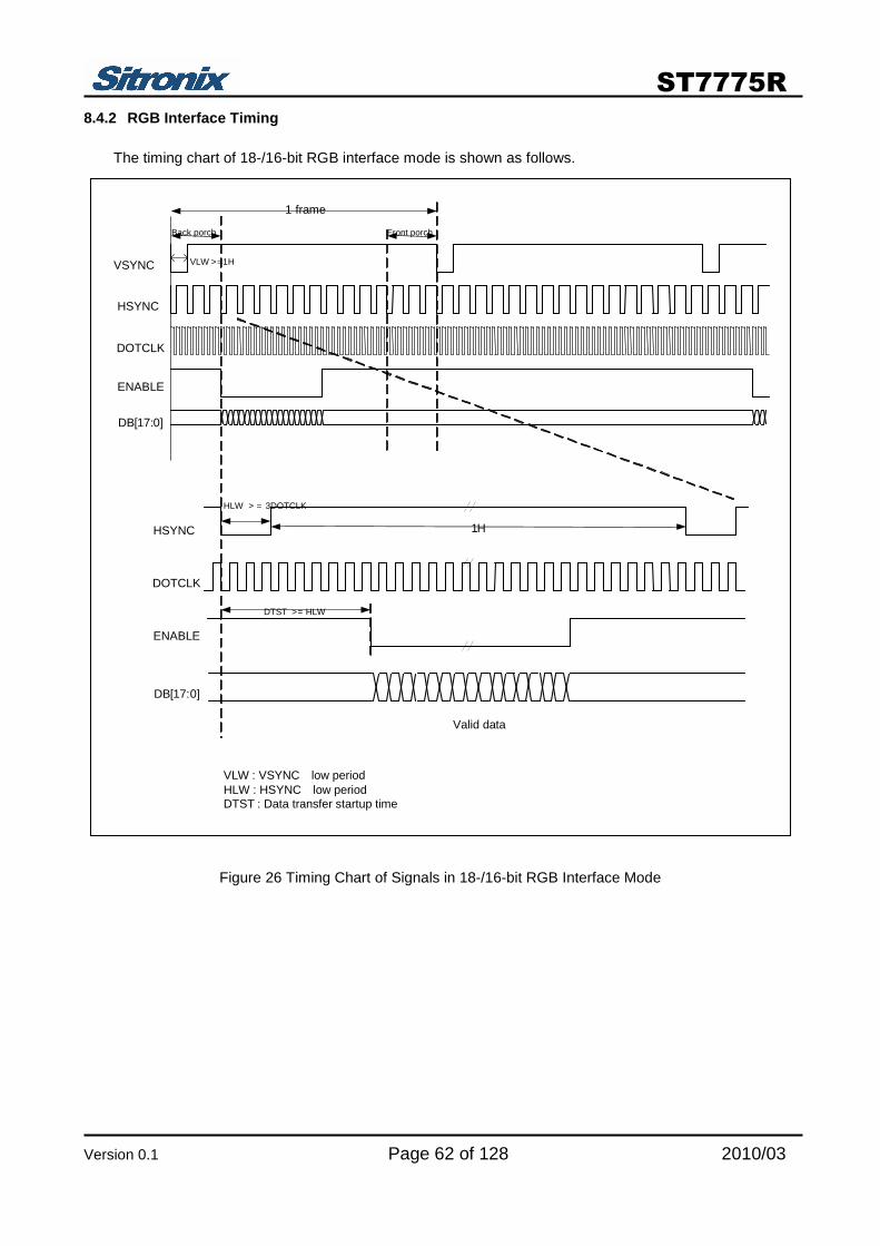
7.4.4 RGB Interface Characteristics:
Figure 6 RGB Interface Timing Characteristics
VDDI=1.65 to 3.3V, VDD=2.5 to 3.3V, AGND=DGND=0V, Ta=25
Signal Symbol Parameter MIN MAX Unit Description
TSYNCS VSYNC, HSYNC Setup Time TBD ns HSYNC,
VSYNC Trghr, Trghf VSYNC, HSYNC Rise/Fall time TBD ns
TENS Enable Setup Time TBD ns ENABLE
TENH Enable Hold Time TBD ns
PWDH DOTCLK High-level Pulse Width TBD ns
PWDL DOTCLK Low-level Pulse Width TBD ns
TCYCD DOTCLK Cycle Time TBD ns DOTCLK
Trghr, Trghf DOTCLK Rise/Fall time TBD ns
TPDS PD Data Setup Time TBD ns DB
TPDH PD Data Hold Time TBD ns
Table 7 18/16 Bits RGB Interface Timing Characteristics
HSYNC VSYNC
DOTCLK
Data Bus Write
V IH
V IL
T SYNCS
ENABLE V
IH V
IL
T ENS T ENH
V IH
V IL V
IH
V IH
V IL
V IH
V IL
Write Data
V IH
V IL
PWDL PWDH
T CYCD
T PDS T PDH
T rgbf T rgbr
T rgbf T rgbr
Page 43
ST7775R
Version 0.1 Page 43 of 128 2010/03
VDDI=1.65 to 3.3V, VDD=2.5 to 3.3V, AGND=DGND=0V, Ta=25
Signal Symbol Parameter MIN MAX Unit Description
TSYNCS VSYNC, HSYNC Setup Time TBD ns HSYNC,
VSYNC Trghr, Trghf VSYNC, HSYNC Rise/Fall time TBD ns
TENS Enable Setup Time TBD ns ENABLE
TENH Enable Hold Time TBD ns
PWDH DOTCLK High-level Pulse Width TBD ns
PWDL DOTCLK Low-level Pulse Width TBD ns
TCYCD DOTCLK Cycle Time TBD ns DOTCLK
Trghr, Trghf DOTCLK Rise/Fall time TBD ns
TPDS PD Data Setup Time TBD ns DB
TPDH PD Data Hold Time TBD ns
Table 8 6 Bits RGB Interface Timing Characteristics
Page 44
ST7775R
Version 0.1 Page 44 of 128 2010/03
8 INTERFACE
8.1.. MCU Interface Type Selection
ST7775R supports 8/16/9/18 bit parallel data bus for 8080 series CPU, 6800 series CPU, RGB serial
interfaces. Selection of these interfaces are set by IM[3:0] pins as shown below.
IM3 IM2 IM1 IM0 Interface Read Back Data Bus Selection
0 0 0 0 6800 MCU16-bit Parallel DB[17:10], DB[8:1]
0 0 0 1 6800 MCU8-bit Parallel DB[17:10]
0 0 1 0 8080 MCU16-bit Parallel DB[17:10], DB[8:1]
0 0 1 1 8080 MCU8-bit Parallel DB[17:10],
0 1 0 ID Serial Peripheral Interface(SPI) SDI, SDO
0 1 1 0 3-wire serial interface CSX,SCL,SDA
0 1 1 1 4-wire serial interface CSX,SCL,SDA,DCX
1 0 0 0 6800 MCU18-bit Parallel DB[17:0]
1 0 0 1 6800 MCU9-bit Parallel DB[17:9]
1 0 1 0 8080 MCU18-bit Parallel DB[17:0]
1 0 1 1 8080 MCU9-bit Parallel DB[17:9]
1 1 -- -- Setting invalid -
Table 9 Interface Type Selection
Page 45
ST7775R
Version 0.1 Page 45 of 128 2010/03
8.2.. 8080-Series MCU Write Cycle Sequence
The write cycle means that the host writes information (command / data) to the display via the interface.
Each write cycle (WRX high-low-high sequence) consists of 3 control signals (DCX, RDX, WRX) and data
signals (DB[17:0]). DCX bit is a control signal, which tells if the data is a command or a data. The data signals
are the command if the control signal is low (=’0’) and vice versa it is data (=’1’).
Figure 7 8080-Series WRX Protocol
Note: WRX is an unsynchronized signal (It can be stopped).
Figure 8 8080-Series Parallel Bus Protocol, Write to Register or Display RAM
Page 46
ST7775R
Version 0.1 Page 46 of 128 2010/03
8.3.. 6800-Series MCU Write Cycle Sequence
The write cycle means that the host writes information (command or/and data) to the display via the interface.
Each write cycle (E low-high-low sequence) consists of 3 control signals (DCX, E, RWX) and data signals
(D[17:0]). DCX bit is a control signal, which tells if the data is a command or a data. The data signals are the
command if the control signal is low (=’0’) and vice versa it is data (=’1’).
Figure 9 6800-Series WRX Protocol
Note: E is an unsynchronized signal (It can be stopped)
Figure 10 6800-Series Parallel Bus Protocol, Write to Register or Display RAM
Page 47
ST7775R
Version 0.1 Page 47 of 128 2010/03
8.3.1 18 bits Interface Write Data Format
The 8080-18bits interface is selected by setting the IM [3:0] =”1010”. The 6800-18bits interface is
selected by setting the IM [3:0] =”1000”.The 18 bits mode only 262k colors format in display. In this interface
write instructions and DRAM method following figure.
MCU ST7775
/CS
A0
/WR
/RD
/RST
D[17:0]
/CS
RS
/WR
/RD
RESET
DB[17:0]18
Figure 11 18 bits Interface Data Format (Command Write/DRAM Write)
Page 48
ST7775R
Version 0.1 Page 48 of 128 2010/03
8.3.2 16 bits Interface Write Data Format
The 8080-16bits interface is selected by setting IM [3:0] =”0010”. The 6800-16bits interface is selected by
setting IM [3:0] =”0000”.The mode can display 262k or 65k colors format. When the 262k color format is
display, two transfers mode is used (first transfer: 2 bits, second transfer: 16 bits or first transfer: 16 bits,
second transfer: 2 bits).
Page 49
ST7775R
Version 0.1 Page 49 of 128 2010/03
Figure 12 16 bits Interface Data Format (Command Write/Display RAM Write)
8.3.3 9 bits Interface Write Data Format
The 8080-9bits interface is selected by setting the IM [3:0] = “1011” The 6800-9bits interface is selected
by setting the IM [3:0] = “1001” and the DB [17:9] pins are used to transfer the data. When writing the 16-bit
register, the data is divided into upper byte and lower byte and the upper byte is transferred first. The display
data is also divided in upper byte (9 bits) and lower byte, and the upper byte is transferred first. The unused
DB [8:0] pins must be tied to either VDDI or DGND.
MCU Driver IC
/CS
A0
/WR
/RD
/RST
D[8:0]
/CS
RS
/WR
/RD
RESET
DB[17:9]
9DB[8:0]
Page 50
ST7775R
Version 0.1 Page 50 of 128 2010/03
Figure 13 9 bits Interface Data Format (Command Write/Display RAM Write)
Page 51
ST7775R
Version 0.1 Page 51 of 128 2010/03
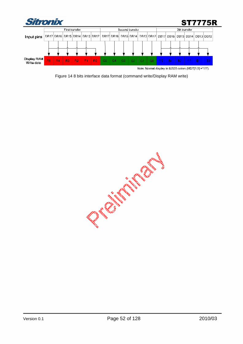
8.3.4 8 bits Interface Write Data Format
The 8080 8-bit interface is selected by setting the IM [3:0] as “0011” The 6800 8-bit interface is selected
by setting the IM [3:0] as “0001” and the DB [17:10] pins are used to transfer the data. The mode can display
262k or 65k colors format. When writing the 16-bit register, the data is divided into upper byte lower byte and
the upper byte is transferred first. The display data is also divided in upper byte (8 bits) and lower byte, and
the upper byte is transferred first. The written data is expanded into 18 bits internally (see the figure below)
and then written into DRAM. The unused DB [9:0] pins must be tied to either VDDI or DGND.
Page 52
ST7775R
Version 0.1 Page 52 of 128 2010/03
Figure 14 8 bits interface data format (command write/Display RAM write)
Page 53
ST7775R
Version 0.1 Page 53 of 128 2010/03
8.3.5 8080-series MCU Read Cycle Sequence
The read cycle (RDX “1”- “0”- “1” sequence) means that the host reads information from display via
interface. The driver sends data (DB [17:0]) to the host when there is a falling edge of RDX and the host reads
data when there is a rising edge of RDX.
Figure 15 8080-Series Read Protocol
Note1: RDX is an unsynchronized signal (It can be stopped)
CMD DM PA CMD DM & data Data DataS P
CMD DM PA CMD DM & Data Data DataS P
“1”
Hi-Z
Read Parameter Read Display Data
CMD: Write Command Code
PA: Parameter or Display Data
DM PA1 DM & data PAN-2 PAN-1 PS
CMD CMDS PHi-Z Hi-Z
Hi-Z
DB[17:0]
RESET
CSX
DCX
(RS)
RDX
WRX
Host DB[17:0]
(Host to LCD)
Driver DB[17:0]
(LCD to Host)
DB[17:0]
Signals on DB[17:0],DCX,WRX,RDX
pins during CSX=1 are ignored
DM: Dummy Read
Figure 16 8080-series parallel bus protocol, read data from register or display RAM
Page 54
ST7775R
Version 0.1 Page 54 of 128 2010/03
8.3.6 6800-series MCU Read Cycle Sequence
The read cycle (E low-high-low sequence) means that the host reads information from LCD driver via
interface. The driver sends data (DB [17:0]) to the host when there is a rising edge of E and the host reads
data when there is a falling edge of E.
Figure 17 6800-Series Read Protocol
Note: E is an unsynchronized signal (It can be stopped)
Figure 18 6800-series parallel bus protocol, read data from register or display RAM
Page 55
ST7775R
Version 0.1 Page 55 of 128 2010/03
8.3.7 18bits interface read data format
Figure 19 18 bits Interface Data Format (Command Read/Display RAM Read)
Page 56
ST7775R
Version 0.1 Page 56 of 128 2010/03
8.3.8 16bits Interface Read Data Format
Figure 20 16 bits Interface Data Format (Command Read/Display RAM Read)
Page 57
ST7775R
Version 0.1 Page 57 of 128 2010/03
8.3.9 9bits Interface Read Data Format
Figure 21 9 bits Interface Data Format (Command Read/Display RAM Read)
Output pins
IB15 IB14 IB13 IB12 IB11 IB10 IB8 IB7 IB6 IB5 IB4 IB3 IB2 IB1IB9 IB0Register data
First Second
First
DB17 DB16 DB15 DB14 DB13 DB12 DB11 DB10 DB17 DB16 DB15 DB14 DB13 DB12 DB11 DB10DB9 DB9
Second
Page 58
ST7775R
Version 0.1 Page 58 of 128 2010/03
8.3.10 8bits Interface Read Data Format
Figure 22 8 bits Interface Data Format (Command Read/Display RAM Read)
Page 59
ST7775R
Version 0.1 Page 59 of 128 2010/03
SS = ’0’ S1 S2 S3 S4 S5 S6 ------ S523 S524 S525 S526 S527 S528
SS = ’1’ S526 S527 S528 S523 S524 S525 ------- S4 S5 S6 S1 S2 S3
BGR=’0’ R G B R G B ------- R G B R G B
GS
= ’1’
GS
= ’0’
BGR=’1’ B G R B G R B G R B G R
X Address “0000”h “0001”h “00AE”h “00AF”h
G220
G1
Y Address “0000”h “0000”h -------
“0000”h “0000”h
X Address “0000”h “0001”h “00AE”h “00AF”h
G219
G2
Y Address “0001”h “0001”h -------
“0001”h “0001”h
|
|
|
|
|
|
|
|
|
|
|
|
|
|
|
|
|
|
|
|
-------
|
|
|
|
|
|
|
|
X Address “0000”h “0001”h “00AE”h “00AF”h G2
G219 Y Address “00DA”h “00DA”h
------- “00DA”h “00DA”h
X Address “0000”h “0001”h “00AE”h “00AF”h G1
G220 Y Address “00DB”h “00DB”h
------- “00DB”h “00DB”h
Figure 23 DRAM Address Map Table
Note:
X Address End Instruction:R36h
X Address Start Instruction:R37h
Y Address End Instruction:R38h
Y Address Start Instruction:R39h
SS/GS ,RGB Setting Instruction:R03h
Page 60
ST7775R
Version 0.1 Page 60 of 128 2010/03
8.4.. RGB Input Interface
The RGB Interface mode for ST7775R is selected by setting the RIM[1:0] bits as following table.
RIM1 RIM0 RGB Interface Mode Data pins
0 0 18-bit RGB Interface DB[17:0]
0 1 16-bit RGB Interface DB[17:13], DB[11:1]
1 0 6-bit RGB Interface DB[17:12]
1 1 Setting prohibited
18-bit RGB Interface ( 262K colors )
DB
17
DB
16
DB
11
DB
12
DB
13
DB
14
DB
15
DB
4
DB
5
DB
6
DB
7
DB
8
DB
10
DB
9
DB
3
DB
0
DB
1
DB
2
WD
17
WD
16
WD
11
WD
12
WD
13
WD
14
WD
15
WD
4
WD
5
WD
6
WD
7
WD
8
WD
10
WD
9
WD
3
WD
0
WD
1
WD
2
R5 R4 G5R0R1R2R3 B4B5G0G1G2G4 G3 B3 B0B1B2
Input Data
Write Data
Register
DRAM Data&
RGB Mapping
16-bit RGB Interface ( 65K colors )
DB
17
DB
16
DB
11
DB
13
DB
14
DB
15
DB
4
DB
5
DB
6
DB
7
DB
8
DB
10
DB
9
DB
3
DB
1
DB
2
WD
17
WD
16
WD
11
WD
13
WD
14
WD
15
WD
4
WD
5
WD
6
WD
7
WD
8
WD
10
WD
9
WD
3
WD
1
WD
2
R5 R4 G5R0R1R2R3 B4B5G0G1G2G4 G3 B3 B0B1B2
6-bit RGB Interface ( 262K colors )
DB
17
DB
16
DB
17
DB
12
DB
13
DB
14
DB
15
DB
16
DB
17
DB
12
DB
13
DB
14
DB
16
DB
15
DB
15
DB
12
DB
13
DB
14
WD
17
WD
16
WD
11
WD
12
WD
13
WD
14
WD
15
WD
4
WD
5
WD
6
WD
7
WD
8
WD
10
WD
9
WD
3
WD
0
WD
1
WD
2
R5 R4 G5R0R1R2R3 B4B5G0G1G2G4 G3 B3 B0B1B2
1st Transfer 2nd Transfer 3rd Transfer
Input Data
Write Data
Register
DRAM Data&
RGB Mapping
Input Data
Write Data
Register
DRAM Data&
RGB Mapping
Figure 24 RGB Interface Data Format
Page 61
ST7775R
Version 0.1 Page 61 of 128 2010/03
8.4.1 RGB Interface
The display operation via the RGB interface is synchronized with the VSYNC, HSYNC, and DOTCLK
signals. The data can be written only within the specified area with low power consumption by using window
address function and high-speed write mode (HWM = 1). The back porch and front porch are used to set the
RGB interface timing.
HSYNC
DOTCLK
DB[17:0]
ENABLE
VSYNC
Back Porch
Period (BP[3:0])
Display Period
(NL[4:0])
Front Porch
Period (FP[3:0])
Moving Picture
Display Area
RAM Data Display Area
Note 1 : Front porth period continues until
the next input of VSYNC.
Note 2 : Input DOTCLK throughout the
operation.
Note 3 : Supply the VSYNC,HSYNC and
DOTCLK with frequency that can meet the
resolution requirement of panel.
Figure 25 DRAM Access Area by RGB Interface
Page 62
ST7775R
Version 0.1 Page 62 of 128 2010/03
8.4.2 RGB Interface Timing
The timing chart of 18-/16-bit RGB interface mode is shown as follows.
Figure 26 Timing Chart of Signals in 18-/16-bit RGB Interface Mode
VSYNC
HSYNC
DOTCLK
ENABLE
DB [ 17 : 0 ]
1 frame
Front porch Back porch
VLW > = 1 H
HSYNC
DOTCLK
ENABLE
DB [ 17 : 0 ]
1 H
Valid data
HLW > = 3 DOTCLK
DTST > = HLW
VLW : VSYNC low period HLW : HSYNC low period DTST : Data transfer startup time
Page 63
ST7775R
Version 0.1 Page 63 of 128 2010/03
The timing chart of 6-bit RGB interface mode is shown as follows.
Figure 27 Timing chart of signals in 6-bit RGB interface mode
VSYNC
HSYNC
DOTCLK
ENABLE
DB [ 17 : 12 ]
1 frame
Front porch Back porch
VLW > = 1 H
HSYNC
DOTCLK
ENABLE
DB [ 17 : 12 ]
1 H
Valid data
HLW > = 3 DOTCLK
DTST > = HLW
VLW : VSYNC low period HLW : HSYNC low period DTST : Data transfer startup time Note 1 : Use the high speed write mode ( HWM = 1 ) to write data through the RGB interface . Note 2 : In 6 - bite RGB interface mode , each dot of one pixel ( R , G and B ) is transferred in synchronization with DOTCLKs . Note 3 : In 6 - bite RGB interface mode , set the cycles of VSYNC , HSYNC and ENABLE to 3 multiples of DOTCLKs .
R G B R G B B R G B
Page 64
ST7775R
Version 0.1 Page 64 of 128 2010/03
8.4.3 Moving Picture Mode
ST7775R has the RGB interface to display moving picture and incorporates DRAM to store display data,
which has following merits in displaying a moving picture.
The window address function defined the update area of DRAM.
The DRAM is updated only the moving picture area.
It can contribute to lower the power consumption of the system by reducing data transfer.
When display the moving picture in RGB interface mode, the DB[17:0] can be switched as system
interface to update still picture area and registers, such as icons.
RAM access via a system interface in RGB-I/F mode
ST7775R allows DRAM access via the system interface in RGB interface mode. In RGB interface mode,
data are written to the internal DRAM in synchronization with DOTCLK while ENABLE signal is “Low”. When
write data to the internal DRAM by the system interface, set ENABLE(“High”) to stop write data via RGB
interface. Then set RM = “0” to enable RAM access via system interface. When restart RAM access in RGB
interface mode, wait one read/write cycle, set RM = “1” and then the index register (R22h) to start accessing
RAM via the RGB interface. If RAM accesses via two interfaces conflicts, there is no guarantee that data are
written to the internal DRAM.
The following figure illustrates the operation of the ST7775R when displaying a moving picture via the
RGB interface and rewriting the still picture RAM area via the system interface.
Page 65
ST7775R
Version 0.1 Page 65 of 128 2010/03
Figure 28 Example of update the still and moving picture
Update
a frame
Update
a frame
Update
moving
picture
area
Update
moving
picture
area
Set IR
to R22h
Set
RM=0
Set
AD[16:0]
Set IR
to R22h
Set
RM=1
Set
AD[16:0]
Set IR
to R22h
Update display
data in other than
the moving
picture area
Write still picture area
VSYNC
ENABLE
DOTCLK
DB[17:0]
Page 66
ST7775R
Version 0.1 Page 66 of 128 2010/03
8.4.4 6-bit RGB Interface
The 6-bit RGB interface is selected by setting the RIM[1:0] bits to “10”. The display operation is
synchronized with VSYNC, HSYNC, and DOTCLK signals. Display data are transferred to the internal DRAM
in synchronization with the display operation via 6-bit RGB data bus (DB[17:12]) according to the data enable
signal (ENABLE). Unused pins (DB[11:0]) must be fixed at GND level. Registers can be set by the system
interface (i80/SPI).
Figure 29 Example of 6-bit RGB interface data format
Data transfer synchronization in 6-bit RGB interface mode
ST7775R has counters to count the first, second, third 6 bit transfers via 6-bit RGB interface. The transfer
counters are always reset to first data on the falling edge of VSYNC from the next frame period. If a mismatch
data transfer occurs, the correct data transfer will be restart via 6 bit interface in next frame period. When data
transfer is consecutively in moving picture operation, this function can help the display system restoring
normal display operation and minimizes effects in occurring mismatch data transfer.
Figure 30 6-bit Transfer Synchronization
Page 67
ST7775R
Version 0.1 Page 67 of 128 2010/03
8.4.5 16-bit RGB Interface
The 16-bit RGB interface is selected by setting the RIM[1:0] bits to “01”. The display operation is
synchronized with VSYNC, HSYNC, and DOTCLK signals. Display data are transferred to the internal RAM in
synchronization with the display operation via 16-bit RGB data bus (DB[17:13], DB[11:1]) according to the
data enable signal (ENABLE). Registers are set only via the system interface.
Figure 31 Example of 16-Bit RGB Interface and Data Format
Page 68
ST7775R
Version 0.1 Page 68 of 128 2010/03
8.4.6 18-bit RGB Interface
The 18-bit RGB interface is selected by setting the RIM[1:0] bits to “00”. The display operation is
synchronized with VSYNC, HSYNC, and DOTCLK signals. Display data are transferred to the internal RAM in
synchronization with the display operation via 18-bit RGB data bus (DB[17:0]) according to the data enable
signal (ENABLE). Registers are set only via the system interface.
RGB Interface With 18-bit Data Bus
DB
17
DB
16
DB
11
DB
12
DB
13
DB
14
DB
15
DB
4
DB
5
DB
6
DB
7
DB
8
DB
10
DB
9
DB
4
DB
0
DB
1
DB
2
R5 R4 G5R0R1R2R3 B4B5G0G1G2G4 G3 B3 B0B1B2
Input Data
RGB
Assignment Figure 32 Example of 18-bit RGB Interface and Data Format
Notes to external display in using the RGB Input Interface
1. The following are the functions not available in RGB Input Interface mode.
Function RGB Interface I80 System Interface
Partial display Not available Available
Scroll function Not available Available
Interlaced scan Not available Available
Graphics operation function Not available Available
2. VSYNC, HSYNC, and DOTCLK signals must be supplied during a display operation period.
3. In RGB interface mode, the panel controlling signals are generated from DOTCLK, not the internal clock
generated from the internal oscillator.
4. In 6-bit RGB interface mode, each of RGB dots are transferred in synchronization with DOTCLK signals.
In other words, one pixel data needs to take three DOTCLKs to transfer.
5. In 6-bit RGB interface mode, the cycles of VSYNC, HSYNC, ENABLE, DOTCLK signals must be set
correctly so that the data transfer is completed in units of pixels.
6. When switching between the internal operation mode and the external display interface operation mode,
follow the sequences below in setting instruction.
7. In RGB interface mode, the front porch period continues until the next VSYNC input is detected after
drawing one frame.
8. In RGB interface mode, a RAM address (AD[16:0]) is set in the address counter every frame on the
falling edge of VSYNC.
Page 69
ST7775R
Version 0.1 Page 69 of 128 2010/03
Figure 33 Internal clock operation/RGB interface mode switching
Page 70
ST7775R
Version 0.1 Page 70 of 128 2010/03
Set DM[1:0]=01 and
RM=0 with RGB
Interface Mode
HWM=1/0
Set AD[16:0]
Set IR to R22h
(DRAM Data Write)
Write Data to DRAM
through System Interface
System Interface Operation
Write Data Through RGB
Interface to Write Data
Through System Interface
RGB Interface Operation
Write Data Through System
Interface to Write Data
Through RGB Interface
System Interface Operation
Write Data to DRAM
through System Interface
HWM=1/0
Set AD[16:0]
Set DM[1:0]=01 and
RM=0 with RGB
Interface Mode
Set IR to R22h
(DRAM Data Write)
RGB Interface Operation
Figure 34 DRAM access between system interface and RGB interface
Page 71
ST7775R
Version 0.1 Page 71 of 128 2010/03
8.5.. Interface Timing
The following are diagrams of interfacing timing with LCD panel control signals in internal operation and
RGB interface.
VSYNC
HSYNC
DOTCLK
ENABLE
1 2 3 4 5 1 2 3 4218 219 220
1 2 3 4 5 218 219 220
DB[17:0]
FLM
G1
G2
G220
.
.
.
S[528:1]
VCOM
Figure 35 Relationship between RGB I/F signals and LCD Driving Signals for Pane
Page 72
ST7775R
Version 0.1 Page 72 of 128 2010/03
8.6.. 24-bit Serial Peripheral Interface (24-bit SPI)
The Serial Peripheral Interface (SPI) is selected by setting the IM[3:0] pins as “010x” level. The chip
select pin (CSX), the serial transfer clock pin (SCL), the serial data input pin (SDI) and the serial data output
pin (SDO) are used in SPI mode. The ID pin sets the least significant bit of the identification code. The
DB[17:0] pins, which are not used, must be tied to GND.
The SPI interface operation enables from the falling edge of CSX and ends of data transfer on the rising
edge of CSX. The start byte is transferred to start the SPI interface and the read/write operation and RS
information are also included in the start byte. When the start byte is matched, the subsequent data is
received by ST7775R.
The seventh bit of start byte is RS bit. When RS = “0”, either index write operation or status read
operation is executed. When RS = “1”, either register write operation or RAM read/write operation is executed.
The eighth bit of the start byte is used to select either read or write operation (R/W bit). Data is written when
the R/W bit is “0” and read back when the R/W bit is “1”.
After receiving the start byte, ST7775R starts to transfer or receive the data in unit of byte and the data
transfer starts from the MSB bit. All the registers of the ST7775R are 16-bit format and receive the first and
the second byte data as the upper and the lower eight bits of the 16-bit register respectively. In SPI mode, 5
bytes dummy read is necessary and the valid data starts from 6th byte of read back data.
Start Byte Format
Transferred bits S 8 7 6 5 4 3 2 1
R/W RS Device IC Code Start byte format Transfer start
1/0 1/0 ID 0 1 1 1 0
Notes: .ID bit is selected by setting the IM0/ID pin
RS and R/W Bit Function
RS R/W Function
0 0 Set an index register
0 1 Read a status
1 0 Write a register or DRAM data
1 1 Read a register or DRAM data
Page 73
ST7775R
Version 0.1 Page 73 of 128 2010/03
Figure 36 Data Format of SPI Interface
Page 74
ST7775R
Version 0.1 Page 74 of 128 2010/03
Figure 37 Data transmission through serial peripheral interface (SPI)
Page 75
ST7775R
Version 0.1 Page 75 of 128 2010/03
(e) Basic data transmission through SPI
CSX(input)
SCL
(input)
SDI(input)
SDO
(output)
0 01 1 1
Start Byte
DRAM data read
Start End
1 3 42 5 6 7 8 10 119 12 13 14 15 16 17 18 19 20 21 22 23 24 25 26 27 28 29 30 31 32
ID RS RW D15 D14 D13D12D11D10 D9 D8 D7 D6 D5 D4 D3 D2 D1 D0D23 D22D21D20 D19D18 D17 D16
DRAM data write
D15 D14 D13D12D11D10 D9 D8 D7 D6 D5 D4 D3 D2 D1 D0D22D21D20 D19D18 D17 D16D23
(f) DRAM data write transmission
CSX
(input)
Start End
SCL
(input)
SDI
(input)
SDO(output)
RAM data 1
1st transferStart ByteRAM data 1
2nd transfer
RAM data 1
3rd transfer
RAM data 2
1st transfer
RAM data 2
2nd transfer
RAM data 2
3rd transfer
DRAM data (1)
execution timeDRAM data (2)
execution time
(g) DRAM data read transmission
CSX
(input)
Start End
SCL(input)
SDI(input)
SDO
(output)
Start byte RS=1,RW=1
Dummy
read 1
Dummy
read 2
RAM read 1st byte
RAM read 2nd byte
RAM read 3rd byte
Note : Five bytes of invalid dummy data read after the start byte.
RAM data transfer in SPI mode when MDT[1] = 1 and MDT[0] = 1 or 0
Figure 38 Data transmission through serial peripheral interface (SPI, MDT[1:0] = ”1 or 0”)
Page 76
ST7775R
Version 0.1 Page 76 of 128 2010/03
8.7.. 9-bit Serial Peripheral Interface (9-bit SPI)
This SPI mode uses a 3-wire 9-bit serial interface. The chip-select CSX (active low) enables and disables the
serial interface. SCL is the serial data clock and SDA is serial data.
Serial data must be input to SDA in the sequence DCX, D7 to D0. The ST7775R reads the data at the rising
edge of SCL signal. The first bit of serial data DCX is data/command flag. When DCX = "1", D7 to D0 bits are
DRAM data or command parameters. When DCX = "0" D7 to D0 bits are commands.
Register Write Mode:
Figure 39 9-bit SPI Write Register Mode
Page 77
ST7775R
Version 0.1 Page 77 of 128 2010/03
Register Read Mode:
When users need to read back the register or DRAM data, the register R66h must be set as “1” first, and then
write the register index to read back the register or DRAM data. The following timing diagrams show
examples to read back the register data.
Figure 40 9-bit SPI Read Register mode
9-bit Serial Data Transfer Interface
Figure 41 9-bit SPI 65K colors Serial Data Transfer,
Page 78
ST7775R
Version 0.1 Page 78 of 128 2010/03
Figure 42 9-bit SPI 262K colors Serial Data Transfer
8.8.. 8-bit Serial Peripheral Interface (8-bit SPI)
This SPI mode uses a 4-wire 8-bit serial interface. The chip-select CSX (active low) enables and disables the
serial interface. DCX is the command or data select signal, SCL is the serial data clock and SDA is serial data.
Serial data must be input to SDA in the sequence D7 to D0. The ST7775R reads the data at the rising edge of
SCL signal. The DCX signal indicates data/command. When DCX = "1", D7 to D0 bits are display RAM data
or command parameters. When DCX = "0" D7 to D0 bits are commands.
Register Write Mode:
Figure 43 8-bit SPI Write Register Mode
Register Read Mode: When users need to read back the register or DRAM data, the register R66h must be set as “1” first, and then
write the register index to read back the register or DRAM data. The following timing diagrams show
examples to read back the register data.
Page 79
ST7775R
Version 0.1 Page 79 of 128 2010/03
Figure 44 8-bit SPI Read Register mode
8-bit Serial Data Transfer
Figure 45 8-bit SPI 65K colors Serial Data Transfer,
Figure 46 8-bit SPI 262K colors Serial Data Transfer
Page 80
ST7775R
Version 0.1 Page 80 of 128 2010/03
8.9.. Data Transfer Recovery
If there is a break in data transmission while transferring a command or DRAM data or multiple register data,
before Bit D0 of the byte has been completed, then the ST7775R will reject the previous bits and have reset
the interface such that it will be ready to receive the same byte retransmitted when the chip select line (CSX)
is next activated. See the following example:
Figure 47 Data Transfer Recovery
If the 2 parameter of command is being sent and a break occurs while sending any parameter before the last
one and if the host then sends a new command rather than re-transmitting the parameter that was interrupted,
then the parameters that were successfully sent are stored and the parameter where the break occurred is
rejected. The interface is ready to receive next byte as show below.
Note: Break can be e.g. another command or noise pulse.
8.10.. Register Descriptions
ST7775R adopts 18-bit bus interface architecture for high-performance microprocessor. All the functional
Blocks of ST7775R starts to work after receiving the correct instruction from the external microprocessor by
the 18-, 16-, 9-, 8-bit interface. The index register (IR) stores the register address to which the instructions and
Display data will be written. The register selection signal (RS), the read/write signals (RDX/WRX) and data
bus D[17:0] are used to read/write the instructions and data of ST7775R. The registers of the ST7775R are
categorized into the following groups.
1. Specify the index of register (IR)
2. Read a status
3. Display control
4. Power management Control
5. Graphics data processing
Page 81
ST7775R
Version 0.1 Page 81 of 128 2010/03
6. Set internal DRAM address (AC)
7. Transfer data to/from the internal DRAM (R22)
8. Internal grayscale γ-correction (R30 ~ R39)
Normally, the display data (DRAM) is most often updated, and in order since the ST7775R can update
internal DRAM address automatically as it writes data to the internal DRAM and minimize data transfer by
using the window address function, there are fewer loads on the program in the microprocessor. The way of
assigning data to the 16 register bits (D[15:0]) varies for each interface. Send registers in accordance with the
following data transfer format.
Figure 48 Register Setting with Serial Peripheral Interface (SPI)
Page 82
ST7775R
Version 0.1 Page 82 of 128 2010/03
i80-18bits Data bus Interface
DB
16
DB
11
DB
12
DB
13
DB
14
DB
15
DB
4
DB
5
DB
6
DB
7
DB
10
DB
9
DB
3
DB
0
DB
1
DB
2
Data Bus
(DB[17:0])
Register
Bit(D[15:0])
DB
8
D
15
D
10
D
11
D
12
D
13
D
14D4D5D6D7D9 D8 D3 D0D1D2
DB
17
i80-16bits Data bus Interface
DB
16
DB
11
DB
12
DB
13
DB
14
DB
15
DB
4
DB
5
DB
6
DB
7
DB
10
DB
3
DB
1
DB
2
Data Bus
(DB[17:10])
(DB[8:1])
Register
Bit(D[15:0])
DB
8
D
15
D
10
D
11
D
12
D
13
D
14D4D5D6D7D9 D8 D3 D0D1D2
DB
17
i80-9bits Data bus Interface
DB
16
DB
11
DB
12
DB
13
DB
14
DB
15
DB
13
DB
14
DB
15
DB
16
DB
10
DB
9
DB
12
DB
9
DB
10
DB
11
Data Bus
(DB[17:9])
Register
Bit(D[15:0])
DB
17
D
15
D
10
D
11
D
12
D
13
D
14D4D5D6D7D9 D8 D3 D0D1D2
DB
17
i80-8bits Data bus Interface / Serial Peripheral Interface (2/3 transmission)
DB
16
DB
11
DB
12
DB
13
DB
14
DB
15
DB
4
DB
5
DB
6
DB
7
DB
10
DB
3
DB
1
DB
2
Data Bus
(DB[17:10])
Register
Bit(D[15:0])
DB
8
D
15
D
10
D
11
D
12
D
13
D
14D4D5D6D7D9 D8 D3 D0D1D2
DB
17
1st Transfer 2nd Transfer
1st Transfer 2nd Transfer
Figure 49 Register setting with i80 System Interface
Page 83
ST7775R
Version 0.1 Page 83 of 128 2010/03
Figure 50 Register Read/Write Timing of i80 System Interface
Page 84
ST7775R
Version 0.1 Page 84 of 128 2010/03
9 COMMAND
9.1.. System Function Command List
No Registers W/R RS D15 D14 D13 D12 D11 D10 D9 D8 D7 D6 D5 D4 D3 D2 D1 D0
IR Index Register W 0 - - - - - - - - ID7 ID6 ID5 ID4 ID3 ID2 ID1 ID0
00h Driver Code Read R 1 0 1 1 1 0 1 1 1 0 1 1 1 0 1 0 1
01h Driver Output Control W/R 1 VSPL HSPL DPL EPL 0 SM GS SS 0 0 0 NL4 NL3 NL2 NL1 NL0
02h LCD Driving Control W/R 1 0 0 0 0 0 0 0 INV 0 0 0 0 0 0 0 0
03h Entry Mode W/R 1 0 0 0 BGR 0 0 MDT1 MDT0 0 0 I/D1 I/D0 AM 0 0 0
07h Display Control 1 W/R 1 0 0 0 TEMON 0 0 0 0 0 0 0 GON CL REV D1 D0
08h Display control 2 W/R 0 0 0 0 FP3 FP2 FP1 FP0 0 0 0 0 BP3 BP2 BP1 BP0 0
0Bh Display Control 4 W/R 1 0 0 0 0 0 0 0 0 0 0 0 0 RTN3 RTN2 RTN1 RTN0
0Ch RGB Display Interface
Control 1 W/R 1 0 0 0 0 0 0 0 RM 0 0 0 DM 0 0 RIM1 RIM0
0Fh Frame Marker Position W/R 1 0 0 0 0 0 0 0 0 0 0 0 0 0 0 0 OSC_EN
10h Power Control 1 W/R 1 0 0 0 0 0 0 0 0 0 0 0 0 0 0 SLP STB
11h Power Control 2 W/R 1 0 0 0 APON 0 0 0 0 0 0 0 0 0 0 0 0
20h Horizontal DRAM
Address Set W/R 1 0 0 0 0 0 0 0 0 AD7 AD6 AD5 AD4 AD3 AD2 AD1 AD0
21h Vertical DRAM Address
Set W/R 1 0 0 0 0 0 0 0 0 AD15 AD14 AD13 AD12 AD11 AD10 AD9 AD8
22h Write Data to GRAM W 1
22h Read Data from GRAM R 1
DRAM Write Data (WD17-0) / Read Data (RD17-0)
28h Software Reset W 1 0 0 0 0 0 0 0 0 0 0 0 0 0 0 0 0
30h Gate Scan Control W/R 1 0 0 0 0 0 0 0 0 0 0 0 SCN4 SCN3 SCN2 SCN1 SCN0
31h Vertical Scroll Control 1 W/R 1 0 0 0 0 0 0 0 0 SEA7 SEA6 SEA5 SEA4 SEA3 SEA2 SEA1 SEA0
32h Vertical Scroll Control 2 W/R 1 0 0 0 0 0 0 0 0 SSA7 SSA6 SSA5 SSA4 SSA3 SSA2 SSA1 SSA0
33h Vertical Scroll Control 3 W/R 1 0 0 0 0 0 0 0 0 SST7 SST6 SST5 SST4 SST3 SST2 SST1 SST0
34h Partial Driving Control 1 W/R 1 0 0 0 0 0 0 0 0 SE17 SE16 SE15 SE14 SE13 SE12 SE11 SE10
35h Partial Driving Control 2 W/R 1 0 0 0 0 0 0 0 0 SS17 SS16 SS15 SS14 SS13 SS12 SS11 SS10
36h Horizontal Address End
Position W/R 1 0 0 0 0 0 0 0 0 HEA7 HEA6 HEA5 HEA4 HEA3 HEA2 HEA1 HEA0
37h Horizontal Address Start
Position W/R 1 0 0 0 0 0 0 0 0 HSA7 HSA6 HSA5 HSA4 HSA3 HSA2 HSA1 HSA0
38h Vertical Address End
Position W/R 1 0 0 0 0 0 0 0 0 VEA7 VEA6 VEA5 VEA4 VEA3 VEA2 VEA1 VEA0
Page 85
ST7775R
Version 0.1 Page 85 of 128 2010/03
39h Vertical Address Start
Position W/R 1 0 0 0 0 0 0 0 0 VSA7 VSA6 VSA5 VSA4 VSA3 VSA2 VSA1 VSA0
50h Gamma Control 1 W/R 1 0 0 0 0 0 KP1[2] KP1[1] KP1[0] 0 0 0 0 0 KP0[2] KP0[1] KP0[0]
51h Gamma Control 2 W/R 1 0 0 0 0 KP3[3] KP3[2] KP3[1] KP3[0] 0 0 0 0 KP2[3] KP2[2] KP2[1] KP2[0]
52h Gamma Control 3 W/R 1 0 0 0 0 0 KP5[2] KP5[1] KP5[0] 0 0 0 0 KP4[3] KP4[2] KP4[1] KP4[0]
53h Gamma Control 4 W/R 1 0 0 SELV63
P[2]
SELV63
P[1]
SELV63
P[0]
SELV62
P[2]
SELV62
P[1]
SELV62
P[0]
SELV1
P[3]
SELV1
P[2]
SELV1
P[1]
SELV1
P[0]
SELV0
P[3]
SELV0
P[2]
SELV0
P[1]
SELV0
P[0]
54h Gamma Control 5 W/R 1 0 0 0 0 VOS0
P[3]
VOS0
P[2]
VOS0
P[1]
VOS0
P[0] 0 0 0 0
VRF0
P[3]
VRF0
P[2]
VRF0
P[1]
VRF0
P[0]
55h Gamma Control 6 W/R 1 0 0 0 0 0 KN1[2] KN1[1] KN1[0] 0 0 0 0 0 KN0[2] KN0[1] KN0[0]
56h Gamma Control 7 W/R 1 0 0 0 0 KN3[3] KN3[2] KN3[1] KN3[0] 0 0 0 0 KN2[3] KN2[2] KN2[1] KN2[0]
57h Gamma Control 8 W/R 1 0 0 0 0 0 KN5[2] KN5[1] KN5[0] 0 0 0 0 KN4[3] PKN4[2] KN4[1] KN4[0]
58h Gamma Control 9 W/R 1 0 0 SELV63
N[2]
SELV63
N[1]
SELV63
N[0]
SELV62
N[2]
SELV62
N[1]
SELV62
N[0]
SELV1
N[3]
SELV1
N[2]
SELV1
N[1]
SELV1
N[0]
SELV0
N[3]
SELV0
N[2]
SELV0
N[1]
SELV0
N[0]
59h Gamma Control 10 W/R 1 0 0 0 0 VOS0
N[3]
VOS0
N[2]
VOS0
N[1]
VOS0
N[0] 0 0 0 0
VRF0
N[3]
VRF0
N[2]
VRF0
N[1]
VRF0
N[0]
65h ID code R 0 0 0 0 0 0 0 0 0 0 0 0 ID3 ID2 ID1 ID0
66h SPI Read/Write Control W/R 1 0 0 0 0 0 0 0 0 0 0 0 0 0 0 0 R/WX
B0h Power Control 3 W/R 1 0 0 VCM5 VCM4 VCM3 VCM2 VCM1 VCM0 0 0 VGLSEL
1
VGLSEL
0 0 0 VGHBT1 VGHBT0
B1h Power Control 4 W/R 1 0 0 0 VRHN4 VRHN3 VRHN2 VRHN1 VRHN0 0 0 0 VRHP4 VRHP3 VRHP2 VRHP1 VRHP0
B2h Power Control 5 W/R 1 0 0 0 0 0 AVCLS2 AVCLS1 AVCLS0 0 0 BCLK_DI
V1 BCLK_DI
V0 0 AVDDS2 AVDDS1 AVDDS0
D2h NVM ID Code W/R 1 0 0 0 0 0 0 0 0 0 0 0 0 ID3 ID2 ID1 ID0
D9h NVM Control Status W/R 1 0 0 0 0 0 0 0 0 0 VMF_EN 0 0 0 0 0 0
DFh NVM Write Command W 1 0 0 0 0 0 0 0 0 1 0 1 0 0 1 0 1
FAh NVM Enable W/R 1 0 0 0 0 0 0 0 0 PROG
_MODE 0 0 0 0 1 MTP
_PROG 0
FEh NVM VCOM Offset W/R 1 0 0 0 0 0 0 0 0 1 0 0 VMF4 VMF3 VMF2 VMF1 VMF0
FFh NVM Command Enable W 1 0 0 0 0 0 0 0 0 0 0 0 0 0 0 CMD1_
EN
CMD2_
EN
Table 10 System Function Command List
Page 86
ST7775R
Version 0.1 Page 86 of 128 2010/03
9.2.. System Function Command
9.2.1 Index (IR)
Note: “-“Don’t care
Index(IR)
RS WRX RDX D15 D14 D13 D12 D11 D10 D9 D8 D7 D6 D5 D4 D3 D2 D1 D0
0 ↑ 1 - - - - - - - - ID7 ID6 ID5 ID4 ID3 ID2 ID1 ID0
Description
The index register specifies the index R00h to RFFh of the control register or RAM control to be
accessed. The access to the register and instruction bits in it is prohibited unless the index is
specified in the index register.
9.2.2 Device ID Code Read (R00h)
Device ID Code Read Out (R00h)
RS WRX RDX D15 D14 D13 D12 D11 D10 D9 D8 D7 D6 D5 D4 D3 D2 D1 D0
1 1 ↑ 0 1 1 1 0 1 1 1 0 1 1 1 0 1 0 1
Description When read this register, the device output device ID code
9.2.3 Device Output Control (R01h)
Device Output Control (R01H)
RS WRX RDX D15 D14 D13 D12 D11 D10 D9 D8 D7 D6 D5 D4 D3 D2 D1 D0
1 ↑ 1 VSPL HSPL DPL EPL 0 SM GS SS 0 0 0 NL4 NL3 NL2 NL1 NL0
Default value 0 0 0 0 0 0 0 0 0 0 0 1 1 1 0 0
Description
VSPL : Sets the signal polarity of the VSYNC pin.
VSPL=”0”, Low active
VSPL=”1”, High active
HSPL : Sets the signal polarity of the HSYNC pin.
HSPL=”0”, Low active
HSPL=”1”, High active
DPL : Sets the signal polarity of the DOTCLK pin.
DPL = “0” The data is input on the positive edge of DOTCLK
DPL = “1” The data is input on the negative edge of DOTCLK
EPL: Sets the signal polarity of the ENABLE pin.
EPL = “0”
The data DB17-0 is written when ENABLE = “0”.
Disable write data operation when ENABLE = “1”
Page 87
ST7775R
Version 0.1 Page 87 of 128 2010/03
EPL = “1”
The data DB17-0 is written when ENABLE = “1”.
Disable write data operation when ENABLE = “0”.
SS: Select the shift direction of outputs from the source driver.
When SS = 0, the shift direction of outputs is from S1 to S528
When SS = 1, the shift direction of outputs is from S528 to S1.
In addition to the shift direction, the settings for both SS and BGR bits are required to change the
Assignment of R, G, B dots to the source driver pins.
To assign R, G, B dots to the source driver pins from S1 to S528, set SS = 0.
To assign R, G, B dots to the source driver pins from S528 to S1, set SS = 1.
Note: When changing SS or BGR bits, DRAM data must be rewritten.
GS: Sets the direction of scan by the gate driver. Set GS bit in combination with SM and SS bits for the
convenience of the display module configuration and the display direction.
SM: Sets the gate driver pin arrangement in combination with the GS bit to select the optimal scan mode
for the module.
SM GS Scan Direction Gate Output Sequence
0 0 TFT Panel
G218G220
G2G4
G217G219
G1G3
Driver IC
Even
Number
G2 to G220
G1 to G219
Odd
Number
G1,G2,G3,G4…..,G220
G217,G218,G219, G220
0 1 TFT Panel
G218G220
G2G4
G217G219
G1G3
Driver IC
Even
Number
G2 to G220
G1 to G219
Odd
Number
G220,G219,…...…G216
G7,G6,G5,G4,G3,G2,G1
Page 88
ST7775R
Version 0.1 Page 88 of 128 2010/03
1 0
G2
G220
G1
G219
Driver IC
TFT Panel
Odd Number
Even Number
G1,G3,G5….……G211
G213,G215,G217,G219
G2,G4,G6….……G212
G214,G216,G218,G220
1 1
G2
G220
G1
G219
Driver IC
TFT Panel
Odd Number
Even Number
G220,G218,….…..G14
G12,G10,G8,G6,G4,G2
G219,G217….….G13
G11,G9,G7,G5,G3,G1
NL [4:0]: Sets the number of lines to drive the LCD at an interval of 8 lines. The DRAM address
mapping is not affected by the number of lines set by NL[4:0]. The number of lines must be the same or
more than the number of lines necessary for the size of the liquid crystal panel.
NL[4:0] LCD Drive Line NL[4:0] LCD Drive Line
6’h00 Reserved
6’h01 8 lines
6’h02 16 lines
.
.
.
.
.
.
6’h03 24 lines 6’h1A 208 lines
6’h04 32 lines 6’h1B 216 lines
6’h05 40 lines 6’h1C 220 lines
9.2.4 LCD Driving Wave Control (R02h)
LCD Driving Wave Control (R02h)
RS WRX RDX D15 D14 D13 D12 D11 D10 D9 D8 D7 D6 D5 D4 D3 D2 D1 D0
1 ↑ 1 0 0 0 0 0 0 0 INV 0 0 0 0 0 0 0 0
Default value 0 0 0 0 0 0 0 0 0 0 0 0 0 0 0 0
Description
INV: VCOM Driving Wave Control.
When INV = 0, the column inversion is selected
When INV = 1, the dot inversion is selected.
Page 89
ST7775R
Version 0.1 Page 89 of 128 2010/03
9.2.5 Entry Mode (R03h)
Entry Mode (R03h)
RS WRX RDX D15 D14 D13 D12 D11 D10 D9 D8 D7 D6 D5 D4 D3 D2 D1 D0
1 ↑ 1 0 0 0 BGR 0 0 MDT1 MDT0 0 0 I/D1 I/D0 AM 0 0 0
Default value 0 0 0 0 0 0 0 0 0 0 1 1 0 0 0 0
Description
AM: Sets the DRAM Update Direction
When AM = “0”, set the horizontal writing direction.
When AM = “1”, set the vertical writing direction.
When a window area is set by registers R36h/R37h and R38h/R39h, only the addressed DRAM area is
updated based on I/D [1:0] and AM bits setting.
I/D [1:0]: Control the address counter (AC) to automatically increase or decrease by 1 when update
one pixel display data.
AM ID[1:0] Write DRAM
Direction AM ID[1:0]
Write DRAM
Direction
0 00
1 00
0 01
1 01
0 10
1 10
Page 90
ST7775R
Version 0.1 Page 90 of 128 2010/03
0 11
1 11
AM I/D[1:0] Register R20/R21 Start Address
R20 00AFh 00
R21 00DBh
R20 0000h 01
R21 00DBh
R20 00AFh 10
R21 0000h
R20 0000h
0/1
11 R21 0000h
BGR: Reverses the order from RGB to BGR in writing 18-bit pixel data in the DRAM.
BGR = 0: Write data in the order of RGB to the DRAM.
BGR=0
D17 D16 D15 D14 D13 D12 D11 D10 D9 D8 D7 D6 D5 D4 D3 D2 D1 D0
R5 R4 R3 R2 R1 R0 G5 G4 G3 G2 G1 G0 B5 B4 B3 B2 B1 B0
BGR = 1: Reverse the order from RGB to BGR in writing data to the DRAM.
BGR=1
D17 D16 D15 D14 D13 D12 D11 D10 D9 D8 D7 D6 D5 D4 D3 D2 D1 D0
] B4 B3 B2 B1 B0 G5 G4 G3 G2 G1 G0 R5 R4 R3 R2 R1 R0
MDT1: This bit is active on the 80-system of 8-bit bus and the data for 1-pixel is transported to the
memory for 3 write cycles. This bit is on the 80-system of 16-bit bus, and the data for 1-pixel is
Transported to the memory for 2 write cycles. When the 80-system interface mode is not set in the 8-bit
or16-bit mode et MDT1 bit to be “0”.
Page 91
ST7775R
Version 0.1 Page 91 of 128 2010/03
MDT0: When 8-bit or16-bit 80 interface mode and MDT1 bit =1, MDT0 defines color depth for the IC.
Interface MDT1 MDT0 Write data to DRAM
0 0 Default transfer value. Multiple data transfer (MDT[1:0]) function is not
available. Data transfer is controlled by interface mode *
0 1 Multiple data transfer (MDT[1:0]) function is not available
1 0
R5 R4 R3 R2 R1 R0 G4 G2 G1 G0 B5 B4 B3 B2G5 B1G3 B0
First Second
DB17 DB16 DB15 DB14 DB13 DB12 DB17 DB16 DB15 DB14 DB13 DB12 DB17 DB16 DB15 DB14 DB13 DB12
Third
8080-8 bit
1 1
Interface MDT1 MDT0 Write data to DRAM
0 1
1 0
DB17 DB16 DB15 DB14 DB13 DB12 DB11 DB10
R5 R4 R3 R2 R1 R0 G4 G2 G1 G0 B5 B4 B3 B2G5 B1G3 B0
DB8 DB7 DB6 DB5 DB4 DB3 DB2 DB1 DB17 DB16
1th Transfer 2th Transfer
8080-16bit
1 1
8bit (8080-8 bit),MDT0=0:262k-coloer (3 times of 6-bit data transfer to DRAM)
8bit (8080-8 bit),MDT0=1:65k-coloer (5-bit,6-bit,5-bit data transfer to DRAM)
8bit (8080-16bit),MDT0=0:262k-coloer (16-bit ,2-bit data transfer to DRAM)
8bit (8080-16 bit),MDT0=1:262k-coloer (2-bit,16-bit data transfer to DRAM)
Page 92
ST7775R
Version 0.1 Page 92 of 128 2010/03
9.2.6 Display Control 1 (R07h)
Display Control 1 (R07h)
RS WRX RDX D15 D14 D13 D12 D11 D10 D9 D8 D7 D6 D5 D4 D3 D2 D1 D0
1 ↑ 1 0 0 0 TEMON 0 0 0 0 0 0 0 GON CL REV D1 D0
Default value 0 0 0 0 0 0 0 0 0 0 0 0 0 0 0 0
Description
D [1:0]: A graphics display is turned on the screen when writing D1 = “1”, and is turned off when writing
D1 = “0”. When writing D1 = “0”, the graphics display data is retained in the internal DRAM and the
ST7775R displays the data when writing D1 = “1”. When D1 = “0”, i.e. while no display is shown on the
panel, all source outputs becomes the GND level to reduce charging/discharging current, which is
generated within the LCD while driving liquid crystal with AC voltage.
When the display is turned off by setting D [1:0] =00, the ST7775R’s internal display operation is halted
completely. In combination with the GON setting, the D [1:0] setting controls display ON/OFF.
D1 D0 GON Source Output Gate Output VCOM Output Display
0 0 X VSS VGL VSS Off
0 VSS VGL VSS Off 0 1
1 VSS Operate VSS Off
0 White on Normally White Panel
Black on Normally Black Panel VGL Operate Off
1 0
1 White on Normally White Panel
Black on Normally Black Panel Operate Operate Off
0 Normally Display VGL Operate Off 1 1
1 Normally Display Operate Operate On
Note1: Data write operation from the microcontroller is performed irrespective of the setting of D [1:0] bits.
GON Set the output level of gate driver G1 ~ G220 as follows
GON G1~G220 Gate Output
0 VGL
1 Normal display
Page 93
ST7775R
Version 0.1 Page 93 of 128 2010/03
CL: When CL = “1”, the ST7775R halt grayscale amplifiers to display 8-color with low power
consumption. When setting 8-color display mode, follow the sequence of 8-color display mode setting
.
CL Display color
0 262,144
1 8
Note: When CL = 1, do not write the data corresponding to the grayscales, for which the operation of amplifier is halted.
REV: Enables the grayscale inversion of the image by setting REV = 1. This enables the ST7775R to
display the same image from the same set of data whether the liquid crystal panel is normally black or
white.
Non- Display Area REV DRAM Data
Positive Polarity Negative Polarity
18’h00000 V63 V0
.
.
.
.
.
.
.
.
.
0
18’h3FFFF V0 V63
18’h00000 V0 V63
.
.
.
.
.
.
.
.
.
1
18’h3FFFF V63 V0
TEMON : TEMON = 1, Enable the Frame flag output signal from the FMARK signal line for preventing
Tearing Effect.
TEMON = 0, Disable the Frame flag output signal from the FMARK signal line for preventing Tearing
Effect.
Page 94
ST7775R
Version 0.1 Page 94 of 128 2010/03
9.2.7 Display Control 2 (R08h)
Display Control 2 (R08h)
RS WRX RDX D15 D14 D13 D12 D11 D10 D9 D8 D7 D6 D5 D4 D3 D2 D1 D0
1 ↑ 1 0 0 0 0 FP3 FP2 FP1 FP0 0 0 0 0 BP3 BP2 BP1 BP0
Default value 0 0 0 0 1 0 0 0 0 0 0 0 1 0 0 0
Description
FP [3:0]: Sets the number of lines for a front porch period (a blank period following the end of
display).
BP [3:0]: Sets the number of lines for a back porch period (a blank period made before the
beginning of display).
Note: In 8080 interface operation mode, BP>=2 lines, FP>=2 lines, BP+FP<=16 lines
In external display interface operation, a back porch (BP) period starts on the falling edge of the
FMARK signal and the display operation starts after the back porch period. A blank period will start
after a front porch (FP) period and it will continue until next FMARK input is detected.
FP[3:0]
BP[3:0] Porch Lines
0000 Setting Prohibited
0001 Setting Prohibited
0010 2 lines
0011 3 lines
0100 4 lines
0101 5 lines
0110 6 lines
0111 7 lines
1000 8 lines
1001 9 lines
1010 10 lines
1011 11 lines
1100 12 lines
1101 13 lines
1110 14 lines
1111 Setting Prohibited
Page 95
ST7775R
Version 0.1 Page 95 of 128 2010/03
Set BP[3:0] and FP[3:0] bits as below for each operation mode
Operation Mode Number of Interlace
Scan Field BP FP BP+FP
FLD=0 BP>=2 BP>=2 FP+BP>=16 8080/6800 System Interface
FLD=0 BP>=3 BP>=5
RGB Interface BP>=2 l BP>=2 FP+BP>=16
Note: BP and FP unit is lines
9.2.8 Frame Cycle Control (R0Bh)
Frame Cycle Control (R0Bh)
RS WRX RDX D15 D14 D13 D12 D11 D10 D9 D8 D7 D6 D5 D4 D3 D2 D1 D0
1 ↑ 1 0 0 0 0 0 0 0 0 0 0 0 0 RTN3 RTN2 RTN1 RTN0
Default value 0 0 0 0 0 0 0 0 0 0 0 0 0 0 0 0
Description
RTNI[3:0]: Sets 1H (line) period. This setting is enabled while the ST7775R’s display operation
is synchronized with internal clock.
RTN[3:0] Clocks/Line
00h 0 clock
01h 1 clock
02h 2 clocks
03h 3 clocks
04h 4 clocks
05h 5 clocks
06h 6 clocks
07h 7 clocks
08h 8 clocks
09h 9 clocks
0Ah 10 clocks
0Bh 11 clocks
0Ch 12 clocks
0Dh 13 clocks
0Eh 14 clocks
0Fh 15 clocks
Page 96
ST7775R
Version 0.1 Page 96 of 128 2010/03
9.2.9 RGB Display Interface Control 1 (R0Ch)
RGB Display Interface Control 1 (R0Ch)
RS WRX RDX D15 D14 D13 D12 D11 D10 D9 D8 D7 D6 D5 D4 D3 D2 D1 D0
1 ↑ 1 0 0 0 0 0 0 0 RM 0 0 0 DM 0 0 RIM1 RIM0
Default value 0 0 0 0 0 0 0 0 0 0 0 0 0 0 0 0
Description
RIM [1:0]: Select the RGB interface data format.
RIM[1:0] RGB Interface Mode
00 18-bit RGB interface (1 transfer/pixel), DB[17:0]
01 16-bit RGB interface (1 transfer/pixel), DB[17:13] and DB[11:1]
10 6-bit RGB interface (3 transfers/pixel), DB[17:12]
11 Setting disabled
Note1: Registers are set only by the system interface.
Note2: Be sure that one pixel (3 dots) data transfer finished when interface switch.
DM [1:0]: Select the display operation mode.
DM[1:0] Display Interface
0 Internal system clock
1 RGB interface
Note1: The DM[1:0] setting allows switching between internal clock operation mode and external display interface
operation mode. However, switching between the RGB interface operation mode and the VSYNC interface operation
mode is prohibited.
RM: Select the interface to access the DRAM.
RM Interface FOR DRAM Access
0 Internal system clock interface
1 RGB interface (when writing display data the RGB interface )
Display Status Operation Mode RAM Access(RM)
Display
Operation
Mode(DM[1:0])
Still picture Internal clock
operation System interface(RM = 0)
Internal clock
operation
(DM = 0)
Moving picture RGB interface (1) RGB interface(RM = 1)
RGB interface
(DM = 1)
Page 97
ST7775R
Version 0.1 Page 97 of 128 2010/03
Rewrite still picture
area while displaying
moving pictures.
RGB interface (2) System interface(RM = 0) RGB interface
(DM = 1)
Note1: Registers are set only via the system interface or SPI interface.
Note2: Refer to the flowcharts of “RGB Input Interface” section for the mode switch.
9.2.10 Oscillator Control (R0Fh)
Oscillator Control (R0Fh)
RS WRX RDX D15 D14 D13 D12 D11 D10 D9 D8 D7 D6 D5 D4 D3 D2 D1 D0
1 ↑ 1 0 0 0 0 0 0 0 0 0 0 0 0 0 0 0 OSC_EN
Default value 0 0 0 0 0 0 0 0 0 0 0 0 0 0 0 1
Description
OSC_EN :This instruction starts the oscillator from the Halt State in the standby mode. After this
instruction,Wait at least 10 ms for oscillation to stabilize before giving the next instruction.
OSC_EN OSC Control
0 OSC. Off
1 OSC. On
9.2.11 Power Control 1 (R10h)
Power Control 1 (R10h)
RS WRX RDX D15 D14 D13 D12 D11 D10 D9 D8 D7 D6 D5 D4 D3 D2 D1 D0
1 ↑ 1 0 0 0 0 0 0 0 0 0 0 0 0 0 0 SLP STB
Default value 0 0 0 0 0 0 0 0 0 0 0 0 0 0 0 0
Description
SLP: When SLP = “1”, ST7775R enters the sleep mode and the display operation stops except the
RC oscillator to reduce the power consumption. No change to the DRAM data and instruction setting
is accepted and he DRAM data and the instruction setting are maintained in SLP mode.
STB: When STB = “1”, ST7775R enters the standby mode and the display operation stops except
the DRAM power supply to reduce the power consumption. No change to the DRAM data and
instruction setting is accepted and he DRAM data and the instruction setting are maintained in STB
mode.
Page 98
ST7775R
Version 0.1 Page 98 of 128 2010/03
9.2.12 Power Control 2 (R11h)
Power Control 2 (R11h)
RS WRX RDX D15 D14 D13 D12 D11 D10 D9 D8 D7 D6 D5 D4 D3 D2 D1 D0
1 ↑ 1 0 0 0 APON 0 0 0 0 0 0 0 0 0 0 0 0
Default value 0 0 0 0 0 0 0 0 0 0 0 0 0 0 0 0
Description
APON: This is an automatic-boosting-operation-starting bit for the booster circuits. In case of
APON=0, the auto booster sequence circuit is stopped. In case of APON=1, booster circuits are
automatically and sequentially operated.
9.2.13 DRAM Horizontal/Vertical Address Set (R20h, R21h)
DRAM Horizontal/Vertical Address Set (R20h,R21h)
RS WRX RDX D15 D14 D13 D12 D11 D10 D9 D8 D7 D6 D5 D4 D3 D2 D1 D0
1 ↑ 1 0 0 0 0 0 0 0 0 AD7 AD6 AD5 AD4 AD3 AD2 AD1 AD0
Default value 0 0 0 0 0 0 0 0 0 0 0 0 0 0 0 0
1 ↑ 1 0 0 0 0 0 0 0 0 AD15 AD14 AD13 AD12 AD11 AD10 AD9 AD8
Default value 0 0 0 0 0 0 0 0 0 0 0 0 0 0 0 0
Description
AD [15:0]:A DRAM address set initially in the AC (Address Counter).The address in the AC is
automatically updated according to the combination of AM, I/D[1:0] settings as the ST7775R writes
data to the internal DRAM so that data can be written consecutively without resetting the address in
the AC.
AD[15:0] DRAM Data Map
16’h0000~16’h00AF 1st line DRAM Data
16’h0100~16’h01AF 2nd line DRAM Data
16’h0200~16’h02AF 3rd line DRAM Data
16’h0300~16’h03AF 4th line DRAM Data
.
.
.
.
.
.
16’h0900~16’HD8AF 218th line DRAM Data
16’h0A00~16’hDAAF 219th line DRAM Data
16’h0B00~16’hDBAF 220h line DRAM Data
Page 99
ST7775R
Version 0.1 Page 99 of 128 2010/03
9.2.14 Write Data to DRAM (R22h)
Write Data to DRAM (R22h)
RS WRX RDX D15 D14 D13 D12 D11 D10 D9 D8 D7 D6 D5 D4 D3 D2 D1 D0
1 ↑ 1 WD [17:0] - DRAM Write Data
Description
WD [17:0]: The ST7775R develops data into 18 bits internally in write operation. The format to
develop data into 18 bits is different in different interface operation. The DRAM data represents the
grayscale level. The DRAM data represents the grayscale level. ST7775R automatically updates
the address to the begin point according to AM and I/D[1:0] settings as it’s wrote this register. The
DFM bit sets the format to develop 16-bit data into the 18-bit data in 16-bit or 8-bit interface
operation.
Page 100
ST7775R
Version 0.1 Page 100 of 128 2010/03
9.2.15 Read Data from DRAM (R22h)
Read Data from DRAM (R22h)
RS WRX RDX D15 D14 D13 D12 D11 D10 D9 D8 D7 D6 D5 D4 D3 D2 D1 D0
1 1 ↑ RD [17:0] - DRAM Read Data
Description
RD [17:0]: 18-bit data read from the DRAM. RAM read data RD [17:0] is transferred via different
data bus in different interface operation. When the ST7775R reads data from the DRAM to the
microcomputer, the first word read immediately after RAM address set is executed is taken in the
internal read-data latch and invalid data is sent to the data bus. Valid data is sent to the data bus
when the ST7775R reads out the second and subsequent words. When either 8-bit or 16-bit
interface is selected, the LSBs of R and B dot data are not read out.
The ST7775R also support function that automatically updates the address according to AM and
I/D[1:0] settings as it read data continuously address in the DRAM
Page 101
ST7775R
Version 0.1 Page 101 of 128 2010/03
Set I/D AM, HAS /HEA, VSA/VEA
Set Address M
Dummy Read (Invalid Data )DRAM -> Read Data Latch
Read Output (Data of Address M)Read Data Latch -> DB[17 : 0]
Auto Counter M=M+1
9.2.16 Softwave Reset (R28h)
Softwave Reset (R28h)
RS WRX RDX D15 D14 D13 D12 D11 D10 D9 D8 D7 D6 D5 D4 D3 D2 D1 D0
1 ↑ 1 0 0 0 0 0 0 0 0 1 1 0 0 1 1 1 0
Description When Software Reset parameter is 00CEh, It cause a software reset. This register automatically
set to Zero after a Software Reset.
Page 102
ST7775R
Version 0.1 Page 102 of 128 2010/03
9.2.17 Gate Scan Control (R30h)
Gate Scan Control (R30h)
RS WRX RDX D15 D14 D13 D12 D11 D10 D9 D8 D7 D6 D5 D4 D3 D2 D1 D0
1 ↑ 1 0 0 0 0 0 0 0 0 0 0 0 SCN4 SCN3 SCN2 SCN1 SCN0
Default value 0 0 0 0 0 0 0 0 0 0 0 0 0 0 0 0
Description
SCN [4:0]: Specifies the gate line where the gate driver starts scan.
Scanning Start Position
SM=0 SM=1 SCN[4:0]
GS=0 GS=1 GS=0 GS=1
00h G1 G220 G1 G220
01h G9 G212 G17 G204
02h G17 G204 G33 G188
03h G25 G296 G49 G172
04h G33 G188 G65 G165
05h G41 G180 G81 G140
06h G49 G172 G97 G124
07h G57 G164 G113 G108
08h G65 G156 G129 G92
09h G73 G148 G145 G76
0Ah G81 G140 G161 G60
0Bh G89 G132 G177 G44
0Ch G97 G124 G193 G28
0Dh G105 G116 G209 G12
0Eh G113 G108 G2 G219
0Fh G121 G100 G18 G203
10h G129 G92 G34 G187
11h G137 G84 G50 G171
12h G145 G76 G66 G155
13h G153 G68 G82 G139
14h G161 G60 G98 G123
15h G169 G52 G114 G107
16h G177 G44 G130 G91
17h G185 G36 G146 G75
18h G193 G28 G162 G59
Page 103
ST7775R
Version 0.1 Page 103 of 128 2010/03
19h G201 G20 G178 G43
1Ah G209 G12 G194 G27
1Bh G217 G4 G210 G11
9.2.18 Vertical Scroll Control1 (R31h,R32h)
Vertical Scroll Control (R31h,R32h)
RS WRX RDX D15 D14 D13 D12 D11 D10 D9 D8 D7 D6 D5 D4 D3 D2 D1 D0 R31h
1 ↑ 1 0 0 0 0 0 0 0 0 SEA7 SEA6 SEA5 SEA4 SEA3 SEA2 SEA1 SEA0
Default value 0 0 0 0 0 0 0 0 1 1 0 1 1 0 1 1
R32h 1 ↑ 1 0 0 0 0 0 0 0 0 SSA7 SSA6 SSA5 SSA4 SSA3 SSA2 SSA1 SSA0
Default value 0 0 0 0 0 0 0 0 0 0 0 0 0 0 0 0
Description
SSA [7:0]: Specify scroll start address at the scroll display for vertical smooth scrolling.
SSA[7:0] Scroll Start Lines
00h 0 line
01h 1 line
02h 2 lines
03h 3 lines
.
.
.
.
.
.
D9h 217 lines
DAh 218 lines
DBh 219 lines
SEA[7:0]: Specify scroll end address at the scroll display for vertical smooth scrolling.
SEA[7:0] Scroll End Lines
00h 0 line
01h 1 line
02h 2 lines
03h 3 lines
.
.
.
.
Page 104
ST7775R
Version 0.1 Page 104 of 128 2010/03
. .
D9h 217 lines
DAh 218 lines
DBh 219 lines
Note1 : Do not set any higher raster-row than 219 (“DB”H).
Note2 : Set SS17-10 _ SSA7-0, if set out of range, SSA7-0 = SS17-10.
Note3 : Set SE17-10 _ SEA7-0, if set out of range, SEA7-0 = SE17-10
9.2.19 Vertical Scroll Control1 (R33h)
Vertical Scroll Control 1(R33h)
RS WRX RDX D15 D14 D13 D12 D11 D10 D9 D8 D7 D6 D5 D4 D3 D2 D1 D0
1 ↑ 1 0 0 0 0 0 0 0 0 SST7 SST6 SST5 SST4 SST3 SST2 SST1 SST0
Default value 0 0 0 0 0 0 0 0 0 0 0 0 0 0 0 0
Description
SST [7:0]: Specify scroll start and step at the scroll display for vertical smooth scrolling. Any line
from the 1st to 220th can be scrolled for the number of the raster-row. After 219th line is displayed,
the display restarts from the first raster-row. When SST [7:0] = 00000000, Vertical Scroll Function is
disabled.
SST[7:0] Scrolling Lines
00h 0 line
01h 1 line
02h 2 lines
03h 3 lines
.
.
.
.
.
.
D9h 217 lines
DAh 218 lines
DBh 219 lines
Note:
1. Do not set any higher raster-row than 219 (“DB”H)
2. Set SS17-10 < SSA7-0 + SST7-0 _ SEA7-0 _ SE17-10, if set out of range, Scroll function is disabled
Page 105
ST7775R
Version 0.1 Page 105 of 128 2010/03
9.2.20 Partial Screen Driving Position (R34h,R35h)
Partial Screen Driving Position (R34h,R35h)
RS WRX RDX D15 D14 D13 D12 D11 D10 D9 D8 D7 D6 D5 D4 D3 D2 D1 D0 R31h
1 ↑ 1 0 0 0 0 0 0 0 0 SE17 SE16 SE15 SE14 SE13 SE12 SE11 SE10
Default value 0 0 0 0 0 0 0 0 1 1 0 1 1 0 1 1
R32h 1 ↑ 1 0 0 0 0 0 0 0 0 SS17 SS16 SS15 SS14 SS13 SS12 SS11 SS10
Default value 0 0 0 0 0 0 0 0 0 0 0 0 0 0 0 0
Description
SE1 [7:0]: Specify the driving end position for the screen in a line unit. The LCD driving is performed to
the ‘set value + 1’ gate driver. For example, when SS1[7:0] = 019h and SE1[7:0] = 029h are set, the
LCD driving is performed from G26 to G42, and non-display driving is performed for G1 to G25, G43,
and others. Ensure that SS1[7:0] <=SE1[7:0]<=DBh.
SS1 [7:0]: Specify the drive starting position for the first screen in a line unit. The LCD driving starts
from the ‘set value +1’ gate driver.
Note: Do not set the partial setting when the operation is in the normal display condition. Set this register only when in the partial
display condition.
9.2.21 Horizontal and Vertical RAM Address Position (R36h, R37h, R38h, R39h)
Horizontal and Vertical RAM Address Position(R36h,R37h,R38h,R39h)
RS WRX RDX D15 D14 D13 D12 D11 D10 D9 D8 D7 D6 D5 D4 D3 D2 D1 D0 R36h
1 ↑ 1 0 0 0 0 0 0 0 0 HEA7 HEA6 HEA5 HEA4 HEA3 HEA2 HEA1 HEA0
Default value 0 0 0 0 0 0 0 0 1 0 1 0 1 1 1 1
R37h 1 ↑ 1 0 0 0 0 0 0 0 0 HSA7 HSA6 HSA5 HSA4 HSA3 HSA2 HSA1 HSA0
Default value 0 0 0 0 0 0 0 0 0 0 0 0 0 0 0 0
R38h 1 ↑ 1 0 0 0 0 0 0 0 0 VEA7 VEA6 VEA5 VEA4 VEA3 VEA2 VEA1 VEA0
Default value 0 0 0 0 0 0 0 0 1 1 0 1 1 0 1 1
R39h 1 ↑ 1 0 0 0 0 0 0 0 0 VSA7 VSA6 VSA5 VSA4 VSA3 VSA2 VSA1 VSA0
Default value 0 0 0 0 0 0 0 0 0 0 0 0 0 0 0
Page 106
ST7775R
Version 0.1 Page 106 of 128 2010/03
Description
HSA [7:0], HEA [7:0] HSA[7:0] and HEA[7:0] are the start and end addresses of the window
address area in horizontal direction, respectively. HSA [7:0] and HEA [7:0] specify the horizontal
range to write data. Set HSA [7:0] and HEA [7:0] before starting RAM write operation. In setting,
make sure that 8’h00 ≤ HAS < HEA ≤ 8’hAF
VSA [7:0], VEA [7:0] VSA [7:0] and VEA [7:0] are the start and end addresses of the window
address area in vertical direction, respectively. VSA [7:0] and VEA [7:0] specify the vertical range to
write data. Set VSA [7:0] and VEA [70] before starting RAM write operation. In setting, make sure
that 9’h000 ≤ VSA < VEA ≤ 8’hDB.
9.2.22 Gamma Control (R50h~R59h)
Gamma Control (R50h~R59h)
RS WRX RDX D15 D14 D13 D12 D11 D10 D9 D8 D7 D6 D5 D4 D3 D2 D1 D0 R50h
1 ↑ 1 0 0 0 0 0 KP1[2] KP1[1] KP1[0] 0 0 0 0 0 KP0[2] KP0[1] KP0[0]
Default value 0 0 0 0 0 0 0 0 0 0 0 0 0 0 0 0
R51h 1 ↑ 1 0 0 0 0 KP3[3] KP3[2] KP3[1] KP3[0] 0 0 0 0 KP2[3] KP2[2] KP2[1] KP2[0]
Default value 0 0 0 0 0 0 0 0 0 0 0 0 0 0 0 0
R52h 1 ↑ 1 0 0 0 0 0 KP5[2] KP5[1] KP5[0] 0 0 0 0 KP4[3] KP4[2] KP4[1] KP4[0]
Default value 0 0 0 0 0 0 0 0 0 0 0 0 0 0 0 0
R53h 1 ↑ 1 0 0
SELV
63P[2]
SELV
63P[1]
SELV
63P[0]
SELV
62P[2]
SELV
62P[1]
SELV
62P[0]
SELV1
P[3]
SELV1
P[2]
SELV1
P[1]
SELV1
P[0]
SELV0
P[3]
SELV0
P[2]
SELV0
P[1]
SELV0
P[0]
Default value 0 0 0 0 0 0 0 0 0 0 0 0 0 0 0 0
R54h 1 ↑ 1 0 0 0 0 VOS0
P[3]
VOS0
P[2]
VOS0
P[1]
VOS0
P[0] 0 0 0 0
VRF0
P[3]
VRF0
P[2]
VRF0
P[1]
VRF0
P[0]
Default value 0 0 0 0 0 0 0 0 0 0 0 0 0 0 0 0
Page 107
ST7775R
Version 0.1 Page 107 of 128 2010/03
R55h 1 ↑ 1 0 0 0 0 0 KN1
[2]
KN1
[1]
KN1
[0] 0 0 0 0 0
KN0
[2]
KN0
[1]
KN0
[0]
Default value 0 0 0 0 0 0 0 0 0 0 0 0 0 0 0 0
R56h 1 ↑ 1 0 0 0 0 KN3
[3]
KN3
[2]
KN3
[1]
KN3
[0] 0 0 0 0
KN2
[3]
KN2
[2]
KN2
[1]
KN2
[0]
Default value 0 0 0 0 0 0 0 0 0 0 0 0 0 0 0 0
R57h 1 ↑ 1 0 0 0 0 0 KN5[2] KN5[1] KN5[0] 0 0 0 0 PKN4
[3]
PKN4
[2]
PKN4
[1]
PKN4
[0]
Default value 0 0 0 0 0 0 0 0 0 0 0 0 0 0 0 0
R58h 1 ↑ 1 0 0 SELV
63N[2]
SELV
63N[1]
SELV
63N[0]
SELV
62N[2]
SELV
62N[1]
SELV
62N[0]
SELV1
N[3]
SELV1
N[2]
SELV1
N[1]
SELV1
N[0]
SELV0
N[3]
SELV0
N[2]
SELV0
N[1]
SELV0
N[0]
Default value 0 0 0 0 0 0 0 0 0 0 0 0 0 0 0 0
R59h 1 ↑ 1 0 0 0 0 VOS0
N[3]
VOS0
N[2]
VOS0
N[1]
VOS0
N[0] 0 0 0 0
VRF0
N[3]
VRF0
N[2]
VRF0
N[1]
VRF0
N[0]
Default value 0 0 0 0 0 0 0 0 0 0 0 0 0 0 0 0
Description
KP5-0[2:0]: γfine Adjustment Register for Positive Polarity.
RP1-0[2:0]: γgradient Adjustment Register for Positive Polarity.
VRP1 [4:0]: γamplitude Adjustment Register for Positive Polarity.
VRP0 [3:0]: γamplitude Adjustment Register for Positive Polarity.
KN5-0[2:0]: γfine Adjustment Register for Negative Polarity.
RN1-0[2:0]: γgradient Adjustment Register for Negative Polarity.
VRN1 [4:0]: γamplitude Adjustment Register for Negative Polarity.
VRN0 [3:0]: γamplitude Adjustment Register for Negative Polarity.
Page 108
ST7775R
Version 0.1 Page 108 of 128 2010/03
9.2.23 ID Code(R65h, Read Only)
Read ID Code (R65h)
RS WRX RDX D15 D14 D13 D12 D11 D10 D9 D8 D7 D6 D5 D4 D3 D2 D1 D0
1 1 ↑ 0 0 0 0 0 0 0 0 0 0 0 0 ID3 ID2 ID1 ID0
Default value 0 0 0 0 0 0 0 0 0 0 0 0 0 0 0 0
Description ID[3:0] This ID code is store in the NV memory to record the LCM vendor code( read only).
9.2.24 SPI Read/Write Control(R66h)
SPI Read/Write Control (R66h)
RS WRX RDX D15 D14 D13 D12 D11 D10 D9 D8 D7 D6 D5 D4 D3 D2 D1 D0
1 ↑ 1 0 0 0 0 0 0 0 0 0 0 0 0 0 0 0 R/WX
Default value 0 0 0 0 0 0 0 0 0 0 0 0 0 0 0 0
Description
R/WX: This register is used to control the read/write function of registers when the 8/9-bit serial
interface is used. If users need to read back the register data by the 8/9-bit serial interface, the R/WX
bit must be set as ‘1’.
R/WX Description
0 Register Write Mode (default)
1 Register Read Mode
Page 109
ST7775R
Version 0.1 Page 109 of 128 2010/03
9.2.25 Power Control 2 (RB0h)
Power Control 2 (RB0h)
RS WRX RDX D15 D14 D13 D12 D11 D10 D9 D8 D7 D6 D5 D4 D3 D2 D1 D0
1 ↑ 1 0 0 VCM5 VCM4 VCM3 VCM2 VCM1 VCM0 0 0 VGLSEL1 VGLSEL0 0 0 VGHBT1 VGHBT0
Default value 0 0 0 0 1 0 0 0 0 0 0 1 0 0 0 1
Description
VCM [5:0]: VCOM voltage setting
VCM[5:0] VCOM VCM[5:0] VCOM
000000 -0.425 100000 -1.225
000001 -0.45 100001 -1.25
000010 -0.475 100010 -1.275
000011 -0.5 100011 -1.3
000100 -0.525 100100 -1.325
000101 -0.55 100101 -1.35
000110 -0.575 100110 -1.375
000111 -0.6 100111 -1.4
001000 -0.625 101000 -1.425
001001 -0.65 101001 -1.45
001010 -0.675 101010 -1.475
001011 -0.7 101011 -1.5
001100 -0.725 101100 -1.525
001101 -0.75 101101 -1.55
001110 -0.775 101110 -1.575
001111 -0.8 101111 -1.6
010000 -0.825 110000 -1.625
010001 -0.85 110001 -1.65
010010 -0.875 110010 -1.675
010011 -0.9 110011 -1.7
010100 -0.925 110100 -1.725
010101 -0.95 110101 -1.75
010110 -0.975 110110 -1.775
010111 -1 110111 -1.8
011000 -1.025 111000 -1.825
011001 -1.05 111001 -1.85
011010 -1.075 111010 -1.875
011011 -1.1 111011 -1.9
011100 -1.125 111100 -1.925
Page 110
ST7775R
Version 0.1 Page 110 of 128 2010/03
011101 -1.15 111101 -1.95
011110 -1.175 111110 -1.975
011111 -1.2 111111 -2
VGLSEL [1:0]: Set the VGH and VGL supply power level.
VGLSEL[1:0] VGL
00 -7.5
01 -10
10 -12.5
11 -13
VGHBT [1:0]: Set the VGH and VGL supply power level.
VGHBT[1:0] VGH
00 2*AVDD+VDD
01 3*AVDD
10 3*AVDD+VDD
11 4*AVDD
Page 111
ST7775R
Version 0.1 Page 111 of 128 2010/03
9.2.26 Power Control 3 (RB1h)
Power Control 3 (RB1h)
RS WRX RDX D15 D14 D13 D12 D11 D10 D9 D8 D7 D6 D5 D4 D3 D2 D1 D0
1 ↑ 1 0 0 0 VRHN4 VRHN3 VRHN2 VRHN1 VRHN0 0 0 0 VRHP4 VRHP3 VRHP2 VRHP1 VRHP0
Default value 0 0 0 0 0 0 1 0 0 0 0 0 0 0 1 0
Description
VRHN/VRHP [4:0]: GVCL/GVDD voltage setting
VRHN[4:0] GVCL VRHP[4:0] GVDD
00000 -4.7 00000 4.7
00001 -4.65 00001 4.65
00010 -4.6 00010 4.6
00011 -4.55 00011 4.55
00100 -4.5 00100 4.5
00101 -4.45 00101 4.45
00110 -4.4 00110 4.4
00111 -4.35 00111 4.35
01000 -4.3 01000 4.3
01001 -4.25 01001 4.25
01010 -4.2 01010 4.2
01011 -4.15 01011 4.15
01100 -4.1 01100 4.1
01101 -4.05 01101 4.05
01110 -4 01110 4
01111 -3.95 01111 3.95
10000 -3.9 10000 3.9
10001 -3.85 10001 3.85
10010 -3.8 10010 3.8
10011 -3.75 10011 3.75
10100 -3.7 10100 3.7
10101 -3.65 10101 3.65
10110 -3.6 10110 3.6
10111 -3.55 10111 3.55
11000 -3.5 11000 3.5
11001 -3.45 11001 3.45
11010 -3.4 11010 3.4
11011 -3.35 11011 3.35
11100 -3.3 11100 3.3
Page 112
ST7775R
Version 0.1 Page 112 of 128 2010/03
11101 -3.25 11101 3.25
11110 -3.2 11110 3.2
11111 -3.15 11111 3.15
9.2.27 Power Control 4 (RB2h)
Power Control 4 (RB2h)
RS WRX RDX D15 D14 D13 D12 D11 D10 D9 D8 D7 D6 D5 D4 D3 D2 D1 D0
1 ↑ 1 0 0 0 0 0 AVCLS2 AVCLS1 AVCLS0 0 0 BCLK
_DIV1
BCLK
_DIV0 0 AVDDS2 AVDDS1 AVDDS0
Default value 0 0 0 0 0 0 1 1 0 0 0 1 0 0 1 1
Description
AVCLS [2:0]: VCL voltage setting
AVCLS[2:0] VCL
000 -4.5
001 -4.6
010 -4.7
011 -4.8
100 -4.9
101 -5
110 -5.1
111 Don’t use this setting, reserve for testing.
BCLK_DIV [1:0]: Boost pumping frequency.
BCLK_DIV[1:0] Frequency (KHz)
00 4000
01 2000
10 1333
11 1000
AVDDS [2:0]: AVDD voltage setting
AVDDS[2:0] AVDD
000 4.5
001 4.6
010 4.7
011 4.8
Page 113
ST7775R
Version 0.1 Page 113 of 128 2010/03
100 4.9
101 5
110 5.1
111 Don’t use this setting, reserve for testing.
9.2.28 NVM ID Code (RD2h)
NVM ID Code (RD2h)
RS WRX RDX D15 D14 D13 D12 D11 D10 D9 D8 D7 D6 D5 D4 D3 D2 D1 D0
1 ↑ 1 0 0 0 0 0 0 0 0 0 0 0 0 ID3 ID2 ID1 ID0
Default value 0 0 0 0 0 0 0 0 0 0 0 0 0 0 0 0
Description ID [3:0]: ST7775R supply 4bit ID code for LCD module version ID
9.2.29 NVM Control Status (RD9h)
NVM Control Status (RD9h)
RS WRX RDX D15 D14 D13 D12 D11 D10 D9 D8 D7 D6 D5 D4 D3 D2 D1 D0
1 ↑ 1 0 0 0 0 0 0 0 0 0 VMF_EN 0 0 0 0 0 0
Default value 0 0 0 0 0 0 0 0 0 0 0 0 0 0 0 0
Description VMF_EN: ”1” = Command NVM VCOM Offset Control (RFEh) Enable.
”0” = Command NVM VCOM Offset Control (RFEh) Disable.
Page 114
ST7775R
Version 0.1 Page 114 of 128 2010/03
9.2.30 NVM Write Command (RDFh)
NVM Write Command (RDFh)
RS WRX RDX D15 D14 D13 D12 D11 D10 D9 D8 D7 D6 D5 D4 D3 D2 D1 D0
1 ↑ 1 0 0 0 0 0 0 0 0 1 0 1 0 0 1 0 1
Description
NVM Write Command.
Command
Parameter
Display
Action
Mode
Legend
Sequential
transter
Wait 20ms
Modify CMD register
(FEh)
CMD D9h, 40h
CMD FEh, xxh
CMD D9h, 00h
Enable NVM :
CMD FFh, 01h
CMD FAh, 86h
External VPP = 7.5V ON
NVM Program Flow
Erase CMD:
CMD DFh, C5h
CMD DFh, A5h
Program CMD:
CMD DFh, 3Ah
CMD DFh, A5h
Wait 20ms
Disable NVM :
CMD FAh, 04h
CMD FFh, 00h
External VPP = 7.5V OFF
Modify CMD register
(D2h)
CMD D2h, xxh
Page 115
ST7775R
Version 0.1 Page 115 of 128 2010/03
9.2.31 NVM Enable (RFAh)
NVM Enable (RFAh)
RS WRX RDX D15 D14 D13 D12 D11 D10 D9 D8 D7 D6 D5 D4 D3 D2 D1 D0
1 ↑ 1 0 0 0 0 0 0 0 0 PROG_MODE 0 0 0 0 1 NVM_PROG 0
Default value 0 0 0 0 0 0 0 0 0 0 0 0 0 1 0 0
Description PROG_MODE: ”1” = Enable NVM digital Function.
NVM_PROG: ”1” =Enable NVM Function.
9.2.32 NVM VCOM Offset (RFEh)
NVM VCOM Offset (RFEh)
RS WRX RDX D15 D14 D13 D12 D11 D10 D9 D8 D7 D6 D5 D4 D3 D2 D1 D0
1 ↑ 1 0 0 0 0 0 0 0 0 1 0 0 VMF4 VMF3 VMF2 VMF1 VMF0
Default value 0 0 0 0 0 0 0 0 1 0 0 1 0 0 0 0
Description
VCMF[4:0]: Set VCOM voltage level for reduce the flicker issue. (“1d”=25mV)
VCMF[4:0] VCOM Output Level
00000 “VCOM”-16d
00001 “VCOM”-15d
| |
01110 “VCOM”-2d
01111 “VCOM”-1d
10000 “VCOM”
10001 “VCOM”+1d
10010 “VCOM”+2d
| |
11110 “VCOM”+14d
11111 “VCOM”+15d
9.2.33 NVM Command Enable (RFFh)
NVM Command Enable (RFFh)
RS WRX RDX D15 D14 D13 D12 D11 D10 D9 D8 D7 D6 D5 D4 D3 D2 D1 D0
1 ↑ 1 0 0 0 0 0 0 0 0 0 0 0 0 0 0 CMD1_EN CMD2_EN
Description CMD2_EN:”1” for enable DFh function.
Page 116
ST7775R
Version 0.1 Page 116 of 128 2010/03
10 RESET FUNCTION
The ST7775R is initialized by the RESET input. During reset period, the ST7775R is in a busy state and
instruction from the MCU and DRAM access are not accepted. The ST7775R’s internal power supply circuit
unit is initialized also by the RESET input. The RESET period must be secured for at least 1ms. In case of
power-on reset, wait until the RC oscillation frequency stabilizes (for 1 ms). During this period, DRAM access
and initial instruction setting are prohibited.
10.1.. System Function Command List
See the Instruction description. The default value is shown in the parenthesis of each instruction bit cell.
10.2.. RAM Data Initialization
The RAM data is not automatically initialized by the RESET input. It must be initialized by software in
display-off period.
10.3.. Note on Reset Function
When a RESET input is entered into the ST7775R while it is in deep standby mode, the ST7775R starts
up the inside logic regulator and makes a transition to the initial state. During this period, the state of the
interface pins may become unstable. For this reason, do not enter a RESET input in deep standby
mode.
When transferring instruction in either two or three transfers via 8-/9-/16-bit interface, make sure to
execute data transfer synchronization after reset operation.
10.4.. Reset Timing Characteristic
Figure 51 Reset Timing
Page 117
ST7775R
Version 0.1 Page 117 of 128 2010/03
VDDI=1.65 to 3.3V, VDD=2.5 to 3.3V, AGND=DGND=0V, Ta=25
Signal Symbol Parameter Min Max Unit Description
TRESL Reset Low Level Width 1 - ms RESET
TREST Reset Complete Time 1 ms -
Table 11 Reset timing Characteristics
Page 118
ST7775R
Version 0.1 Page 118 of 128 2010/03
11 8 - COLOR DISPLAY MODE
The ST7775R has a function to display in 8 colors. In this display mode, only V0 and V63 are used and
power supplies to other grayscales are turned off to reduce power consumption. In 8-color display mode, the
γ-adjustment registers KP0~5, SELV0~1P, SELV62~63P, KN0~5, SELV0~1N, SELV62~63N, are disabled
and the power supplies to V1 to V62 are halted. The ST7775R does not require DRAM data rewrite for 8-color
display by writing the MSB to the rest in each dot data to display in 8 colors.
Grayscale
Amplifie
r
Figure 52 8-Color Display Mode
Page 119
ST7775R
Version 0.1 Page 119 of 128 2010/03
12 WINDOW ADDRESS FUNCTION
The window address function enables writing display data consecutively in a rectangular area (a window
address area) made on the internal DRAM. The window address area is made by setting the horizontal
address register (star: HAS[7:0], end HEA[7:0] bits) and the vertical address register(start: VSA[7:0], end:
VEA[7:0] bits) The AM bits sets the transition direction of RAM address(either increment or decrement).
These bits enable the ST7775R to write data including image data consecutively not taking data wrap
positions into account.
The window address area must be made within the DRAM address map area. Also, DRAM address bits
(RAM address set register) must be an address within the window address area.
[Window address setting area]
(Horizontal direction) 00H ≦ HSA[7:0] ≦ HEA[7:0] ≦ ”AF”H
(Vertical direction) 00H ≦VSA[7:0] ≦ VEA[7:0] ≦ ”BD”H
[RAM address, AD (an address within a window address area)]
(RAM address) HSA[7:0] ≦AD[7:0] ≦HEA[7:0]
VSA[7:0] ≦AD[15:8] ≦VEA[7:0]
Figure 53 DRAM Access Window Map
Page 120
ST7775R
Version 0.1 Page 120 of 128 2010/03
13 GAMMA CORRECTION
The structure of grayscale amplifier is shown as below. 16 voltage levels between GVDD and VSS are
determined by the high/ mid/ low level adjustment registers. Each mid-adjustment level is split into 64 levels
again by the internal ladder resistor network. As a result, grayscale amplifier generates 64 voltage levels
ranging from V0 to V63 and outputs one of 64 levels.
0~60
R
0~60R
8
3
11
23
11
4
8
16
16
16
8
16
16
8
8
Figure 54 Grayscale Voltage Generation (Positive)
Page 121
ST7775R
Version 0.1 Page 121 of 128 2010/03
0~60
R
0~60R
8
3
11
23
11
4
8
16
16
16
8
16
16
8
8
Figure 55 Grayscale Voltage Generation (Negative)
Page 122
ST7775R
Version 0.1 Page 122 of 128 2010/03
Figure 56 Relationship between Source Output and VCOM
Figure 57 Relationship between DRAM Data and Output Level
Page 123
ST7775R
Version 0.1 Page 123 of 128 2010/03
14 APPLICATION
14.1.. Configuration of Power Supply Circuit
Figure 58 Power Supply Circuit Block
The following table shows specifications of external elements connected to the ST7775R power supply circuit. Items Recommended Specification Pin Connection
1 µF Capacity 6.3 V AVCL, AVDD
Table 12 Outside Components
Page 124
ST7775R
Version 0.1 Page 124 of 128 2010/03
14.2.. Standby Mode
Figure 59 Standby Mode Register Setting Sequence
Page 125
ST7775R
Version 0.1 Page 125 of 128 2010/03
14.3.. Power Supply Configuration
When supplying and cutting off power, follow the sequence below. The setting time for oscillators, circuits
and operational amplifiers depends on external resistance and capacitance.
Figure 60 Power Supply ON/OFF Sequence
Page 126
ST7775R
Version 0.1 Page 126 of 128 2010/03
14.4.. Voltage Generation
The pattern diagram for setting the voltages and the waveforms of the voltages of the ST7775R are as
follows.
Figure 61 Power Booster Level
Page 127
ST7775R
Version 0.1 Page 127 of 128 2010/03
14.5.. Applied Voltage to the TFT panel
Figure 62 Voltage Output to TFT LCD Panel
Page 128
ST7775R
Version 0.1 Page 128 of 128 2010/03
15 REVISION HISTORY
Version Date Description
0.1 2010/03 First issue