29
Stacked Horizontal Nanowire based 3-D Integration for Future High Performance Computing Mostafizur Rahman ([email protected]) University of Missouri-Kansas City

Stacked Horizontal Nanowire based 3-D Integration for Future High Performance Computing
MostafizurRahman([email protected])UniversityofMissouri-KansasCity

In Memory Circuits
Beyond CMOS Boolean
Gates
Asymmetric Circuits
Digital FETs
Analog FETs
Detector Receiver
Spin torque(SFET, ASL, STO..)
Straintronics(MESH,MTJ)
Memristor(TMO, 2-D insulators..)
PCM (GST, GES..)
TFET(III-V, gnTFET..)
3-D circuits
Approximate gates
Probabilistic circuits
Neural Nets
Synaptic Circuit
Implication Logic
Majority Logic
Multivalued Circuits
Threshold Gates Binary
Gates
Circuit Layer
Device Layer
BeyondCMOSOpportunities
Ferroelectric(NCFET, P-
FET..)
Quantum Gates
Quantum Search
Quantum Algorithms
Gates Entangler
Architecture/Application Layer
SRC:IntelBCB2017,SRCNRI,ITRS
FETs
FETs
Spin
RRAM
Qubit

IntegratedTSV
WireBonding
TSVStackedMemory
HeterogenousDieswithTSVs
Monolithic3-D
SingleWafer
Multi-ChipPlanar WireandPadBonding
SiliconInterposer
2.5-D
3-D
2-D
LogicDensity
Wafer-Wafer
Die-Die
Device-Device
3-DICClassification
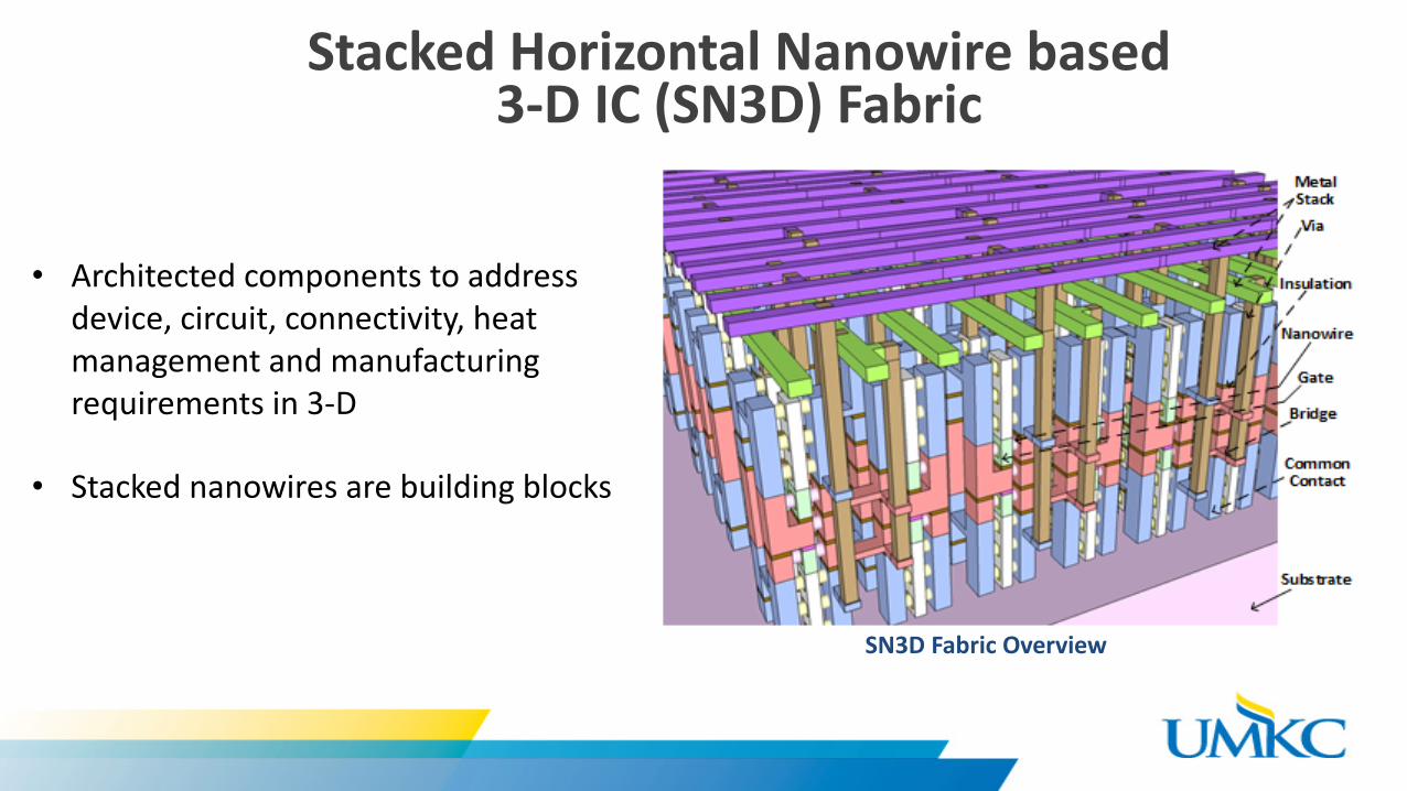
SN3DFabricOverview
• Architectedcomponentstoaddressdevice,circuit,connectivity,heatmanagementandmanufacturingrequirementsin3-D
• Stackednanowiresarebuildingblocks
StackedHorizontalNanowirebased3-DIC(SN3D)Fabric
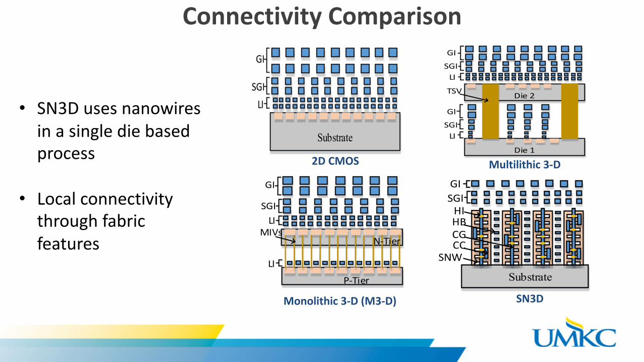
ConnectivityComparison
SGI
Substrate
GI
LI
Substrate
SGIGI
HIHBCGCC
SNW
MIVs
GI
SGILI
LI
N-Tier
P-Tier
TSV
GI
LI
Die2
SGI
GI
LISGI
Die12DCMOS
Monolithic3-D(M3-D)
Multilithic 3-D
SN3D
• SN3Dusesnanowiresinasinglediebasedprocess
• Localconnectivitythroughfabricfeatures

Outline
• SN3DCoreComponentsandLogic• Benchmarking• ThermalManagement• CostAnalysis

Gate(TiN)
Gate(Ti)
(ii)CommonGate
CoreComponents
• FabricassemblybyIntegrationofcorecomponents• Intrinsicthermalmanagement– starkcontrasttoother3-Ddirection
StackedNanowires
NWChannelGateOxide(HfO2)Contact
Gate(Ti/TiN)Spacer(Si3N4)
(i)CommonContact
Contact(Ni)
Contact(Al)
Junctionless Transistor
Nanowires
(iii)HorizontalBridge
BridgeHorizontalIsolation(SU8/SiO2)
HorizontalInsulation(HI)
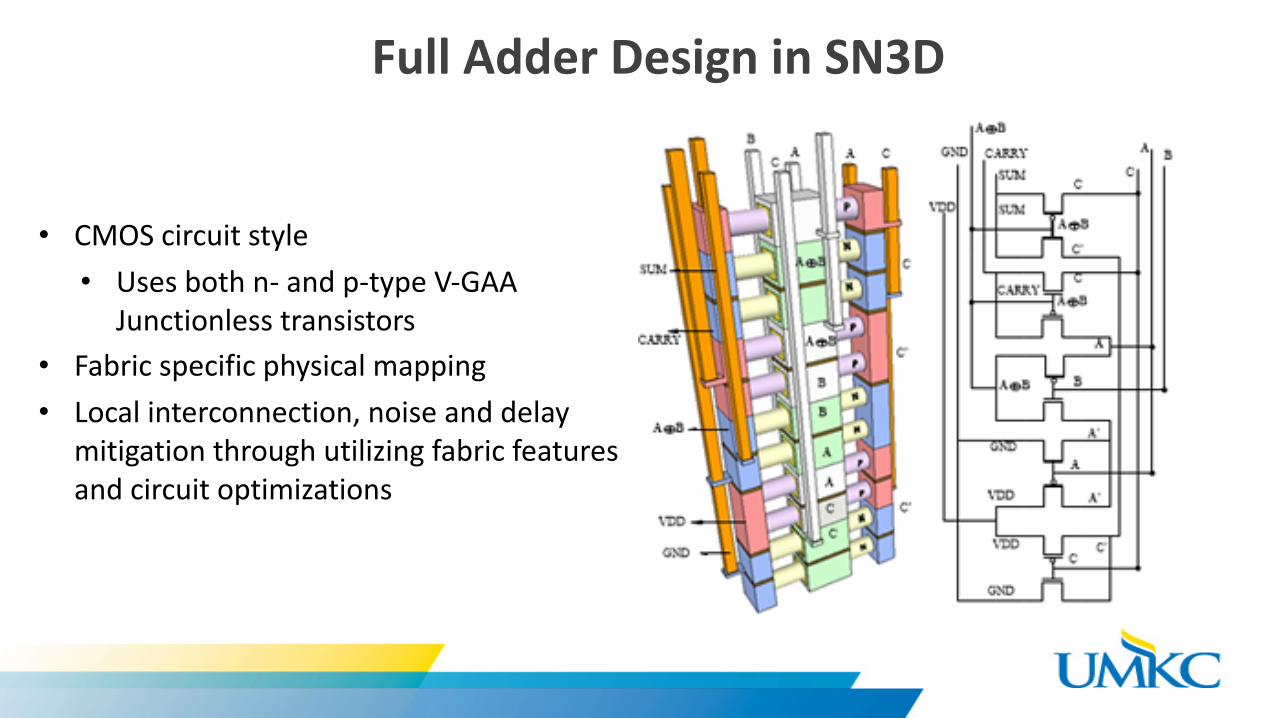
• CMOScircuitstyle• Usesbothn- andp-typeV-GAA
Junctionlesstransistors• Fabricspecificphysicalmapping• Localinterconnection,noiseanddelay
mitigationthroughutilizingfabricfeaturesandcircuitoptimizations
FullAdderDesigninSN3D

• Fabricspecificphysicalmapping• Highdrivestrengthtransistors• Stacked(series)Inverters– CC-CG
SRAMCellDesigninSN3D
ParallelNanowires(3xTpd) Inverter(X1)– 1xTpu:3xTpd
CGCC CCCG
CC CC
D
D
Vdd
Gnd
Vdd
Gnd D
D
X1
X2
Gnd
Gnd
Vdd
Vdd
DD
DD
TA1Wl
Bl
Bl WlTA2
Sp-nw
St1 St2
HB-CC
HB
HB
Wl
Wl
Bl
Bl
Bl Bl
Tpd
Vdd
Vdd
Vdd
Gnd
Gnd
D
D
X1
X2
Gnd
Tpu
Tpu
Tpd
Tpd
TA1
TA2

SN3DSRAMArrayOrganizationandBenefits
TwoAdjacentCells
2 13
45 5
Topview
C25 5
4
3
12
4
C1
C1 C2Bl
Gnd
WlVddWl
Bl
Bl
Gnd
Bl
-Metal2-Metal1
MetalRoutedLayout
• SharingFVs(BL, BL,Wl,Vdd,Gnd)– 2EffectiveFVsforeachcell• 3DAbutmentofadjacentCells
SRAMArrayinSN3D
Bl
Bl
Gnd
Wl Vdd Wl
Bl
Bl
Gnd
Bl
Bl
Gnd
Bl
Bl
Gnd
Bl
Bl
Gnd
GndWl Vdd Wl Wl Vdd Wl Wl Vdd Wl

DesignBenefits
Gnd
Gnd
Bl
WlVdd
z
45l
26 l
Bl
6T-Cell2D-CMOSLayout
PMOSt ier
Wl
Bl
NMOStier
Vdd Gnd VddBl
27l
30l
6T-CellM3DLayout
Bl
Gnd
VddWl
Bl
Bl
Gnd
Bl 27l
14l6T-CellSN3DLayout
• 3:2:1ratioforalldesigns• TSVsaddadditionalareaoverhead• M3Dislimitedtotwotierdesign,only30%reductioninfootprint• M3Dneedshighprecisionalignmentofinter-tier-vias

Benchmarking:MethodologyExperimental
Results
SN3DTCADProcessSimulation
3-DTCADDeviceI-VSimulation
3-DTCADDeviceC-VSimulation
DeviceModelingforHSPICEsimulation
SN3DCircuitandLayoutDesign:Logic,SRAMetc.,
InterconnectExtraction(PTMModel)
RCcalculations
DensityEvaluation
DesignRule
SN3DCircuit(Logic,SRAM)HSPICESimulation
Functionality,PowerandPerformanceEvaluation

BenchmarkingResults
Performance/powerforSN3DandM3Dvs.2-D
• 6.4xperformance/power,67%areareductionforSRAM
• >10xareareduction,19%and18%performanceandpowerimprovementsforlogic
0
20
40
60
80
100
120
PERC
ENTA
GE
2-D MONOLITHIC3D SN3D
PercentageReductioninSRAMFootprint
30.7%
67.8%
LogicBenchmarkingResults
RM=175.87mV
D(V)0.0 0.2 0.4 0.6 0.8 1.0
1.0
0.2
0.4
0.6
0.8
0.0
D(V
)
WM=380.25mV
D(V)0.0 0.2 0.4 0.6 0.8 1.0
1.0
0.2
0.4
0.6
0.8
0.0
D(V
)
HM=325.54mV
0.0 0.2 0.4 0.6 0.8 1.0
1.0
0.2
0.4
0.6
0.8
0.0
HM=325.54mV
D(V
)
D(V)NoiseMargin
0 1 2 3 4 5 6 7
1
SN3D M3D 2-D
6.4X
1.2X
[2] Naveen Macha, Sandeep Geedipally, Mostafizur Rahman, NANOARCH 2017, pp. 155-161, 2017.[3] N. K. MacHa, and M. Rahman, IEEE Transactions on Computer-Aided Design of Integrated Circuits and Systems, 2017, submitted.
[1] N. K. MacHa, M. A. Iqbal, and M. Rahman, NANOARCH, 2016, pp. 51-152.
Outline
• SN3DCoreComponentsandLogic• Benchmarking• ThermalManagement• CostAnalysis
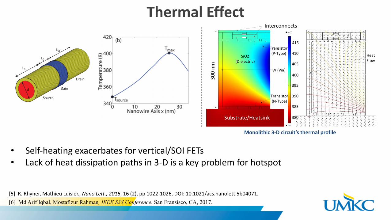
ThermalEffect
[5] R. Rhyner, Mathieu Luisier., Nano Lett., 2016, 16 (2), pp 1022-1026, DOI: 10.1021/acs.nanolett.5b04071.[6] Md Arif Iqbal, Mostafizur Rahman, IEEE S3S Conference, San Fransisco, CA, 2017.
300nm
Transistor(P-Type)
Interconnects
W(Via)
Substrate/Heatsink
SiO2(Dielectric)
Transistor(N-Type)
HeatFlow
415
410
405
400
395
390
385
380
• Self-heatingexacerbatesforvertical/SOIFETs• Lackofheatdissipationpathsin3-Disakeyproblemforhotspot
Monolithic3-Dcircuit’sthermalprofile

ThermalSimulationMethodology
• TheConductiveheattransferinsolidsisobtainedby:ρCp ∂T/∂t+∇ .(-k∇T)=Q
• FiniteElementBasedMethod(FEM)forfine-grainedmodeling
Region Material Dimension(LxWxT)nm
ThermalConductiv
ityWm-1 K-1
Drain Silicide 10x16x16 45.9Drain
Electrode
Ti 10x16x12 21
Channel DopedSi 16x16x16 13Source Silicide 10x16x16 45.9GateOxide HfO2 16x18x2 0.52
GateElectrod
eTiN 10x16x6 1.9
Spacer Si3N4 10x16x16 1.5
DEVICE MATERIALS AND THEIRDIMENSIONSThermalModelingof
Interconnects,Contacts.Powerrails,SignalNanowires,Devices
andPowerPillars
ThermalModelingof3-DCircuit
3-DCircuitLayout
HeatFluxfromHSPICEElectrical
Simulations
Calibration
3-DThermalProfile
EquivalentElectricalRepresentationandHSPICESimulation
FEMThermalSimulations
FEMMethodThermalCircuitSimulationMethod

ThermalSimulationResults(FEM)
• Temperaturereductionby53%to375Kfrom700K• HeatPillarwaseffectivelydissipatingheatfromheatedregion
FETbasedCircuitwithFeatures TransientThermalBehaviorofeachFETwithandwithoutFeatures

ThermalSimulationResults(FEM)
• HeatPillarcanbesharedamongneighboringFETs
• Highesttemperaturewas375Kfortoptransistors
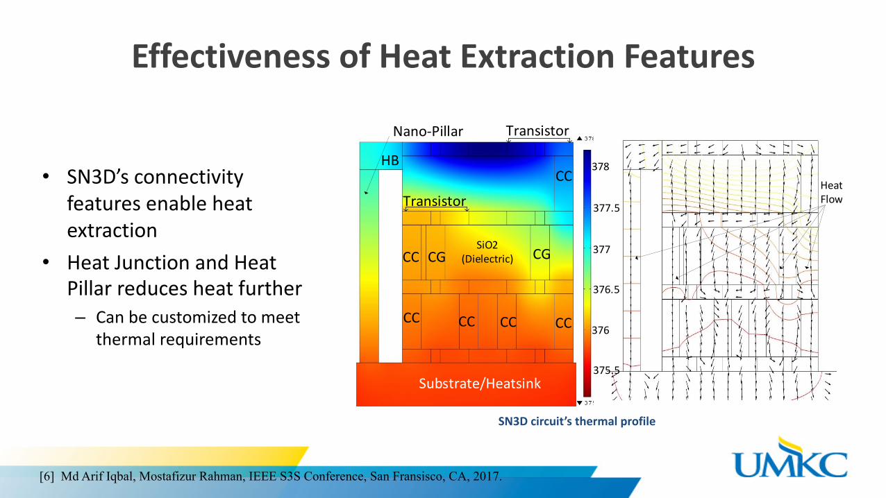
EffectivenessofHeatExtractionFeatures
• SN3D’sconnectivityfeaturesenableheatextraction
• HeatJunctionandHeatPillarreducesheatfurther– Canbecustomizedtomeet
thermalrequirements
HeatFlow
Nano-Pillar
Substrate/Heatsink
SiO2(Dielectric)
CC
CC
CG
CC
CG
CC
CC
CC
Transistor
Transistor
HB 378
377.5
377
376.5
376
375.5
SN3Dcircuit’sthermalprofile
[6] Md Arif Iqbal, Mostafizur Rahman, IEEE S3S Conference, San Fransisco, CA, 2017.

Outline
• SN3DCoreComponentsandLogic• Benchmarking• ThermalManagement• CostAnalysis
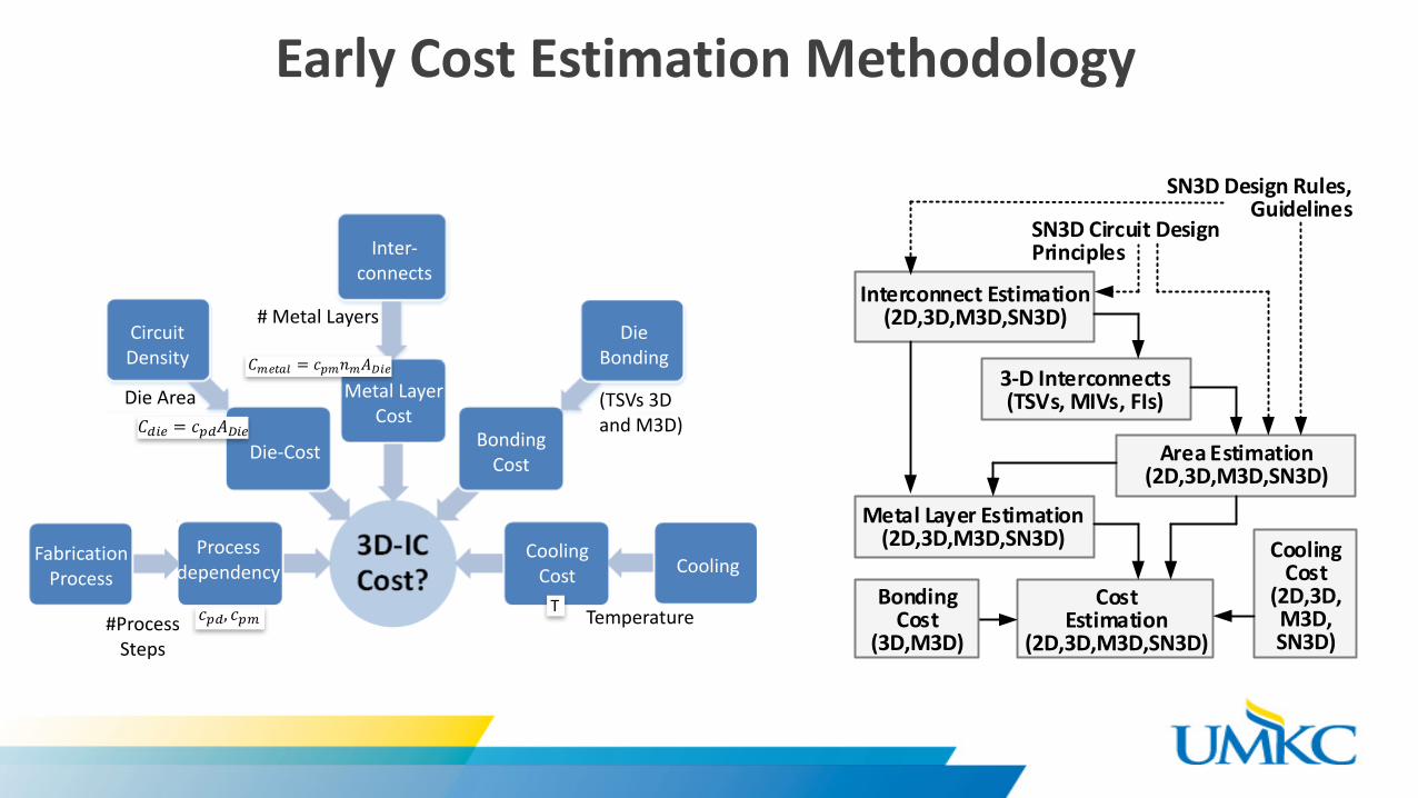
EarlyCostEstimationMethodology
(TSVs3DandM3D)
DieArea
#MetalLayers
#ProcessSteps
Temperature
CoolingCost
BondingCost
MetalLayerCost
Die-Cost
Processdependency
𝐶$%& = 𝑐)$𝐴+%&
𝐶-&./0 = 𝑐)-𝑛-𝐴+%&
𝑐)$, 𝑐)-T
Inter-connects
CircuitDensity
FabricationProcess
DieBonding
Cooling
SN3DDesignRules,Guidelines
SN3DCircuitDesignPrinciples
AreaEstimation(2D,3D,M3D,SN3D)
InterconnectEstimation(2D,3D,M3D,SN3D)
MetalLayerEstimation(2D,3D,M3D,SN3D)
CostEstimation
(2D,3D,M3D,SN3D)
3-DInterconnects(TSVs,MIVs,FIs)
CoolingCost
(2D,3D,M3D,SN3D)
BondingCost
(3D,M3D)

DieAreaEstimation4
3.5
3
2.5
2
1.5
1
0.5
Area(mm
2 )
5.0E+06 10.0E+06 20.0E+06Ng-Numberofgatesinthedesign
0
0.5
1
1.5
2
2.5
3
3.5
4
4.5
5.00E+06 1.00E+07 2.00E+07
A2D
A3D
AM3D
ASN3D
SN3DArea
2DArea3DAreaM3DArea
AverageGateArea2-D:
AverageGateArea3-D/M3D:
SN3DAverageGateArea:
86%,72%and74%reductioninfootprintcomparedto2D,T3DandM3Drespectively[7]
3125 l2 [8]
AreaComparison
3125 l2
2432l2
𝐴4+/678+ = 𝑁:𝐴:,4+/678+𝐴8+/;8+ = 𝑁:𝐴:,8+/;8+ +𝑁=6>/;?>𝐴=6>/;?>
SN3DGateArea
[7] N. K. MacHa and M. Rahman, IEEE S3S Conference, San Fransisco, CA, 2017.[8] X. Dong, J. Zhao, and Y. Xie, IEEE Trans. Comput. Des. Integr. Circuits Syst., vol. 29, no. 12, pp. 1959–1972, 2010.

Rent’s Correlation for Terminal Count:
InterconnectEstimation
[2] N. K. MacHa and M. Rahman, Available: https://arxiv.org/abs/1709.01965.[7] N. K. MacHa and M. Rahman, IEEE S3S Conference, San Fransisco, CA, 2017.
𝐼= = 𝛼𝑘𝑁:(1 − 𝑁:)F [2]
𝑇678+ = H𝑇%
I
%JK
= 𝑛𝑘𝑁:𝑛
)
Total Interconnect
𝑖 𝑙 = 𝑓(𝑁:, 𝑙, 𝑘, 𝑝)[7] ;Distribution
InterconnectDensityFunctio
n,i(l)
1.0E-01
1.0E+00
1.0E+01
1.0E+02
1.0E+03
1.0E+04
1.0E+05
1.0E+06
1.0E+07
1 10 100 1000 10000
1E71E6
1E5
1E3
1E21E1
1E0
0 10 100 10001E-1
1E4
i(l)2D i(l)3D i(l)SN3D
Interconnectlength,l[Gatepitches]
1.0E-06
1.0E-04
1.0E-02
1.0E+00
1.0E+02
1.0E+04
1.0E+06
1 10 100 1000InterconnectLength,l (gatepitches)
InterconnectDensity
Function,i(
l)
1.0E-06
1.0E-04
1.0E-02
1.0E+00
1.0E+02
1.0E+04
1.0E+06
1 10 100 1000 10000
Metal1
Metal2
.
.
Metali
.
Metaln
Lav,1Lav,2
...
Lav,i
...
Lav,i
METAL LAYER ESTIMATION Ng 2-D CMOS TSV 3D M 3D SN3D 5 M 5 5 3 3 10 M 6 5 4 3 20 M 7 6 5 4
MetalLayerEstimates
12%32%
16%
18%22%
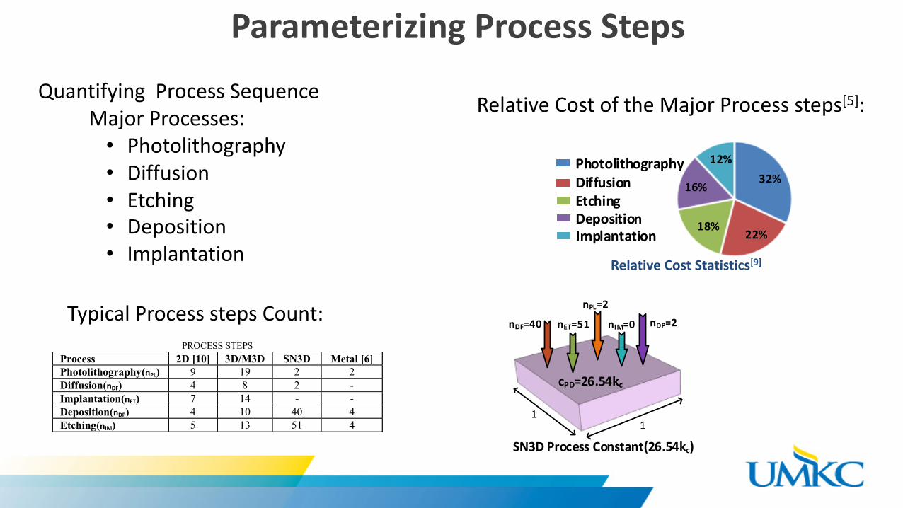
PhotolithographyDiffusionEtchingDepositionImplantation
ParameterizingProcessSteps
SN3DProcessConstant(26.54kc)
nPL=2
nIM=0nDF=40 nET=51 nDP=2
11
cPD=26.54kc
PROCESS STEPS Process 2D [10] 3D/M3D SN3D Metal [6] Photolithography(nPL) 9 19 2 2 Diffusion(nDF) 4 8 2 - Implantation(nET) 7 14 - - Deposition(nDP) 4 10 40 4 Etching(nIM) 5 13 51 4
RelativeCostoftheMajorProcesssteps[5]:
TypicalProcessstepsCount:
QuantifyingProcessSequenceMajorProcesses:
• Photolithography• Diffusion• Etching• Deposition• Implantation RelativeCostStatistics[9]

12%32%
16%
18%22%
PhotolithographyDiffusionEtchingDepositionImplantation
nPL=numberofPhotolithographystepsnDF=numberofDiffusionstepsnET=numberofEtchingstepsnDP=numberofDeposit ionstepsnIM=numberofImplantationsteps UnitProcessConstant(kc)
cPD=kc
nPL=1nIM=1nDF=1 nET=1 nDP=1
11
ParameterizingProcessSteps
SN3DProcessConstant(26.54kc)
nPL=2
nIM=0nDF=40 nET=51 nDP=2
11
cPD=26.54kc
PROCESS STEPS Process 2D [10] 3D/M3D SN3D Metal [6] Photolithography(nPL) 9 19 2 2 Diffusion(nDF) 4 8 2 - Implantation(nET) 7 14 - - Deposition(nDP) 4 10 40 4 Etching(nIM) 5 13 51 4
Arbitraryunitprocessconstant: RelativeCostoftheMajorProcesssteps[5]:
TypicalProcessstepsCount:
RelativeCostStatistics[9]
𝐶678+= 26.54𝑘U𝐴678+ +
2𝑘U𝑛-𝐴678+ +𝐶UVV0%IW
𝑘U = 𝑘XY + 𝑘+Z + 𝑘[= + 𝑘+X + 𝑘?; 𝑘XY = 0.32𝑘U; 𝑘+Z = 0.22𝑘U; 𝑘[= = 0.18𝑘U;𝑘+X = 0.16𝑘U; and𝑘?; = 0.12𝑘U
[6] N. K. MacHa and M. Rahman, Available: https://arxiv.org/abs/1709.01965.[9] Y. Lai, “Cost Per Wafer,” Imid 2009, pp. 1069–1072, 2009.[10] James D. Plummer, et al., ed. New Jersy: Prentice-Hall, 2000, ch. 2, pp. 49–92.

CostEstimationResults
𝐶4+ = 6.26𝑘U𝐴4+ + 2𝑘U𝑛-𝐴4+ +𝐶UVV0%IW𝐶8+/𝐶;8+ = 7.26𝑘U𝐴8+ + 2𝑘U𝑛-𝐴8+ +𝐶dVI$%IW + 𝐶UVV0%IW
𝐶678+ = 26.54𝑘U𝐴678+ + 2𝑘U𝑛-𝐴678+ + 𝐶UVV0%IW
• NoBondingCostforSN3D• BondingCostforTSV3-DandM3-Daretakenasarelativecostfrom[11]
• CoolingCost:1 𝐶UVV0%IW = 𝐾U𝑇 + 𝑐
FinalCostModels:
0
10
20
30
40
50
60
70
80
90
100
COST2D COST3D COSTM3D COSTSN3D2D0
10
20
30
40
50
60
70
80
Ng-Numberofgatesinthedesign
Priceinun
itsofK
c
90
3D M3D SN3D
Diecost
CoolingcostBondingcostMetalcost
CostComparisonResults
[11] X. Dong, J. Zhao, and Y. Xie, IEEE Trans. Comput. Des. Integr. Circuits Syst., vol. 29, no. 12, pp. 1959–1972, 2010.
83%and81%reductionintotalcostcompared2-DCMOSMonolithic3-Dintegration
[7] N. K. Macha and M. Rahman, IEEE S3S Conference, San Fransisco, CA, 2017.

[13] D. Sacchetto, et al., ESSDERC, Athens, Greece,September 14-18, 2009.
SN3DImplementationAspects
[12] M. Rahman, et al., “Skybridge : 3-D IntegratedCircuit Technology Alternative to CMOS,” pp. 44.
[14] Ricky M. Y. Ng et al., IEEE ElectronDevice Lett., vol. 30, no. 5, pp. 520–522,2009.
[15]M.Rahman,etal.,IEEENANO2015-15thInt.Conf.Nanotechnol.,pp.1214–1217,2016.

Summary
• BeyondCMOSopportunitiesspandifferentapplicationdomains
• 3-DIntegrationisobviouschoiceformovingforward– Highestadvantagewithmonolithic3-D
• SN3Disanewstackednanowirebased3-DICtechnique– Integrateddevice,circuit,connectivityandheatmanagement– Possibilityof>10xdensitybenefits– 83%costreductioncomparedto2-DCMOS

Acknowledgements
• CsabaAndrasMoritz(Umass Amherst)• SantoshKhasanvis (Bluerisc)• Pritish Narayanan(IBM)• MasudChowdhury(UMKC)• KelinKuhn(Cornell,prev.Intel)
SponsorsNSF,Univ.ofMissouriResearchFund


