pss applications and materials science a status solidi www.pss-a.com physica REPRINT Raman spectroscopy of WO 3 nano-wires and thermo-chromism study of VO 2 belts produced by ultrasonic spray and laser pyrolysis techniques B. W. Mwakikunga 1, 2, 3 , E. Sideras-Haddad 2 , A. Forbes 4, 5 , and C. Arendse 1 1 CSIR National Centre for Nano-Structured Materials, P.O. Box 395, Pretoria 0001, South Africa 2 School of Physics, University of the Witwatersrand, Private Bag X3, P.O. Wits, Johanneburg 2050, South Africa 3 Department of Physics and Biochemical Sciences, University of Malawi, The Polytechnic, Private Bag 303, Chichiri, Blantyre 3, Malawi 4 CSIR National Laser Centre, P.O. Box 395, Pretoria 0001, South Africa 5 School of Physics, University of Kwazulu-Natal, Private Bag X54001, Durban 4000, South Africa Received 2 May 2007, accepted 25 October 2007 Published online 15 January 2008 PACS 63.22.+m, 73.63.Bd, 78.30.Hv, 81.07.Bc, 81.15.Rs, 81.16.Mk Novel optical and electrical properties of newly synthesized nano-wires of monoclinic WO 3 and nano-belts of rutile VO 2 have been investigated by Raman spectroscopy and thermo- chromism studies respectively. Phonon confinement is ob- served in the WO 3 nano-wires and the previously modified Richter equation is fitted to the experimental Raman spec- troscopy data to obtain the optical phonon dispersion rela- tions for the 713 cm –1 branch and the 808 cm –1 branch of WO 3 phonon spectra for the first time. Electrical measure- ments on the VO 2 nano-belts at varying temperature reveal an enhanced hysteresis width of about 83 °C surpassing previ- ously reported values on the thermo-chromism studies on VO 2 . phys. stat. sol. (a) 205, No. 1, 150 – 154 (2008) / DOI 10.1002/pssa.200776829
Transcript
p s sapplications and materials science
a
statu
s
soli
di
www.pss-a.comph
ysi
ca
REPRINT
Raman spectroscopy of WO3
nano-wires and thermo-chromism studyof VO2 belts produced by ultrasonic sprayand laser pyrolysis techniques
B. W. Mwakikunga1, 2, 3, E. Sideras-Haddad2, A. Forbes4, 5, and C. Arendse1
1
CSIR National Centre for Nano-Structured Materials, P.O. Box 395, Pretoria 0001, South Africa
2
School of Physics, University of the Witwatersrand, Private Bag X3, P.O. Wits, Johanneburg 2050, South Africa
3
Department of Physics and Biochemical Sciences, University of Malawi, The Polytechnic, Private Bag 303, Chichiri, Blantyre 3,
Malawi
4
CSIR National Laser Centre, P.O. Box 395, Pretoria 0001, South Africa
5
School of Physics, University of Kwazulu-Natal, Private Bag X54001, Durban 4000, South Africa
Raman spectroscopy of WO3 nano-wires and thermo-chromism study of VO2 belts produced by ultrasonic spray and laser pyrolysis techniques
B. W. Mwakikunga1, 2, 3, E. Sideras-Haddad*, 2, A. Forbes4, 5, and C. Arendse1
1 CSIR National Centre for Nano-Structured Materials, P.O. Box 395, Pretoria 0001, South Africa 2 School of Physics, University of the Witwatersrand, Private Bag X3, P.O. Wits, Johanneburg 2050, South Africa 3 Department of Physics and Biochemical Sciences, University of Malawi, The Polytechnic, Private Bag 303, Chichiri, Blantyre 3,
Malawi 4 CSIR National Laser Centre, P.O. Box 395, Pretoria 0001, South Africa 5 School of Physics, University of Kwazulu-Natal, Private Bag X54001, Durban 4000, South Africa
1 Introduction Single crystalline semiconductor nano-wires are being extensively investigated due to their unique electronic and optical properties and their novel use in electronic and photonic devices. These unique properties arise from their anisotropic geometry, large surface-to-volume ratio, and carrier and photon/phonon confinement in two dimensions (1D system). More focus, in terms of electronic and photonic applications, is currently directed towards controlled synthesis and characterization of nano-wires (NWs) rather than nano-tubes (NTs) due to inability to control the electronic properties of NTs during synthesis. By contrast, the ability to rationally fabricate NWs with precisely controlled and tuneable chemical composition, size, structure and morphology and to accurately dope them with both p- and n-type dopants has opened up op-portunities for assembling almost any kind of functional nano-system ranging from integrated solid-state photonics
and electronics to biological sensors [1]. For example, NWs have been organized into field effect transistors, bi-polar junction transistors, integrated logic calculators, high frequency ring oscillators and biological and chemical sen-sors, with some having detection limits down to a single virus [2]. Nano-photonic devices such as light-emitting di-odes (LEDs), waveguides, electrically-driven single NW-based lasers, photo-detectors and avalanche photodiodes have all been successfully demonstrated [3]. WO3 and VO2 rutile (VO2 (R)) are transition metal ox-ides (TMOs) whose properties are superior in their respec-tive families of WO
x and VO
x (x is the O/metal ratio). At
room temperature they both adopt distorted structures of some more symmetrical TMOs respectively ReO3 and TiO2 [4]. WO3 has been used as an active layer with outstanding electro-chromic [5], gaso-chromic [6] and photo-chromic [7] properties. For this reason, WO3 has been used to con-
Novel optical and electrical properties of newly synthesized
nano-wires of monoclinic WO3 and nano-belts of rutile VO2
have been investigated by Raman spectroscopy and thermo-
chromism studies respectively. Phonon confinement is ob-
served in the WO3 nano-wires and the previously modified
Richter equation is fitted to the experimental Raman spec-
troscopy data to obtain the optical phonon dispersion rela-
tions for the 713 cm–1 branch and the 808 cm–1 branch of
WO3 phonon spectra for the first time. Electrical measure-
ments on the VO2 nano-belts at varying temperature reveal an
enhanced hysteresis width of about 83 °C surpassing previ-
ously reported values on the thermo-chromism studies on
struct flat panel displays, photo-electro-chromic ‘smart’ windows [8], writing-reading-erasing optical devices [9], optical modulation devices [10], gas sensors and humidity and temperature sensors [11]. On the other hand, VO2 is thermo-chromic [12] and due to this structural change, de-pending on ambient temperature, VO2 has a myriad of quite similar application to WO3: energy efficient windows, optic disc media and holographic storage, bit recording, write-erase stable devices ultra fast switches and I.R. and radar camouflage and laser protection in the military [12]. For a perfect crystal of diameter d having vibrational modes of momentum q, the Heisenberg’s uncertainty prin-ciple (δd δq ~ h) means that as δd → ∞ (bulk) then δq → 0 (the q = 0 selection rule applies). As the diameter, δd → 0 (nano-metric) then the vibrational momentum, δq → ∞. In this case, a contribution from the q ≠ 0 pho-nons determined by the dispersion relation ω(q) is allowed. This accounts for the asymmetric broadening of the peaks in a Raman spectrum. The Richter equation for confined phonons in spherical nano-particles [15], modified to in-clude Gaussian distribution of the phonon momenta and particle size by Faucet and Campbell [16], and further modified to account for the geometry of nano-wires by Adu et al. [11, 17] has been used herein to obtain phonon dispersion spectra for WO3. Thermo-chromism – the ability to change VO2 (R)’s colour at different ambient temperatures – is one of this material’s many important optical properties. This colour change displays a hysteresis around 68 °C. The hysteresis width (HW) determines the materials stability especially when used in optical data storage and optical/electrical switching applications. HW values in the range 1−10 °C have been reported by DeNatale et al. (1989) (in Ref. [14]). We have reported an HW of 5 °C in VO2 (R) produced by ultrasonic spray pyrolysis [12]. A remarkably enhanced hysteresis was report by Lopez et al. [14] to the value of 34 °C on which we have made an improvement in the cur-rent study as discussed in the results section.
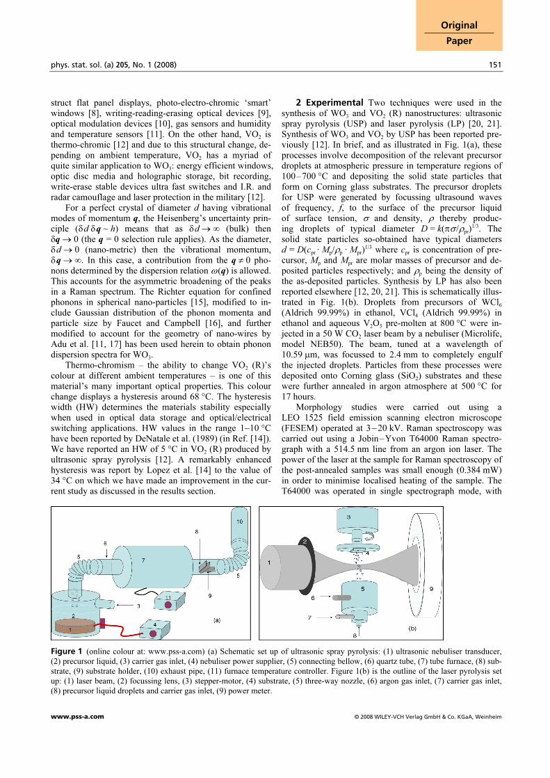
2 Experimental Two techniques were used in the synthesis of WO3 and VO2 (R) nanostructures: ultrasonic spray pyrolysis (USP) and laser pyrolysis (LP) [20, 21]. Synthesis of WO3 and VO2 by USP has been reported pre-viously [12]. In brief, and as illustrated in Fig. 1(a), these processes involve decomposition of the relevant precursor droplets at atmospheric pressure in temperature regions of 100–700 °C and depositing the solid state particles that form on Corning glass substrates. The precursor droplets for USP were generated by focussing ultrasound waves of frequency, f, to the surface of the precursor liquid of surface tension, σ and density, ρ thereby produc- ing droplets of typical diameter D = k(πσ /ρpr)
1/3. The solid state particles so-obtained have typical diameters d = D(cpr · Mp/ρp · Mpr)
1/3 where cpr is concentration of pre-cursor, Mp and Mpr are molar masses of precursor and de-posited particles respectively; and ρp being the density of the as-deposited particles. Synthesis by LP has also been reported elsewhere [12, 20, 21]. This is schematically illus-trated in Fig. 1(b). Droplets from precursors of WCl6 (Aldrich 99.99%) in ethanol, VCl4 (Aldrich 99.99%) in ethanol and aqueous V2O5 pre-molten at 800 °C were in-jected in a 50 W CO2 laser beam by a nebuliser (Microlife, model NEB50). The beam, tuned at a wavelength of 10.59 µm, was focussed to 2.4 mm to completely engulf the injected droplets. Particles from these processes were deposited onto Corning glass (SiO2) substrates and these were further annealed in argon atmosphere at 500 °C for 17 hours. Morphology studies were carried out using a LEO 1525 field emission scanning electron microscope (FESEM) operated at 3−20 kV. Raman spectroscopy was carried out using a Jobin–Yvon T64000 Raman spectro-graph with a 514.5 nm line from an argon ion laser. The power of the laser at the sample for Raman spectroscopy of the post-annealed samples was small enough (0.384 mW) in order to minimise localised heating of the sample. The T64000 was operated in single spectrograph mode, with
Figure 1 (online colour at: www.pss-a.com) (a) Schematic set up of ultrasonic spray pyrolysis: (1) ultrasonic nebuliser transducer,
the 1800 lines/mm grating and a 20× objective on the mi-croscope. The Richter equation given in Refs. [17, 18] and herein reproduced as Eq. (1) was fitted to experimental data and the pertinent parameters were extracted:
( )
2 2
0 2 2
0
exp2
( ) 2π d( ) /4
d
αI ω A
ω ω Γ
^
^ ^
È Ê ˆ ˘-• Á ˜Í ˙Ë ¯Í ˙=- +Í ˙-•
Í ˙Î ˚
Ú
q
q qq
. (1)
In the equation, d is the nano-wire diameter, α is the scal-ing factor, Γ0 is the full-width-at-half-maximum (FWHM) for bulk material Raman peak (Γ0 = 6.5 cm–1 for WO3) [18], q⊥ signifies the momentum vectors perpendicular to the
wire length, ω(q) is the phonon dispersion curve relation (PDR) for the material, A = 713 cm–1, a = 0.76 nm for the 713 cm–1 phonon branch whereas A = 808 cm–1 and b = 0.38 nm [22–25] for the 808 cm–1 phonon branch. For the purposes of the fitting session, the phonon disper- sion relation, ω 2(q) = A2 + AB sin2 (aq) + B2 sin4 (aq), was derived from the simple relation of the form ω(q) = A + Ba
2q
2. The latter assumes isotropic dispersion curves [26]; however the former provided a much smoother fit than the latter for the present WO3 Raman spectroscopy
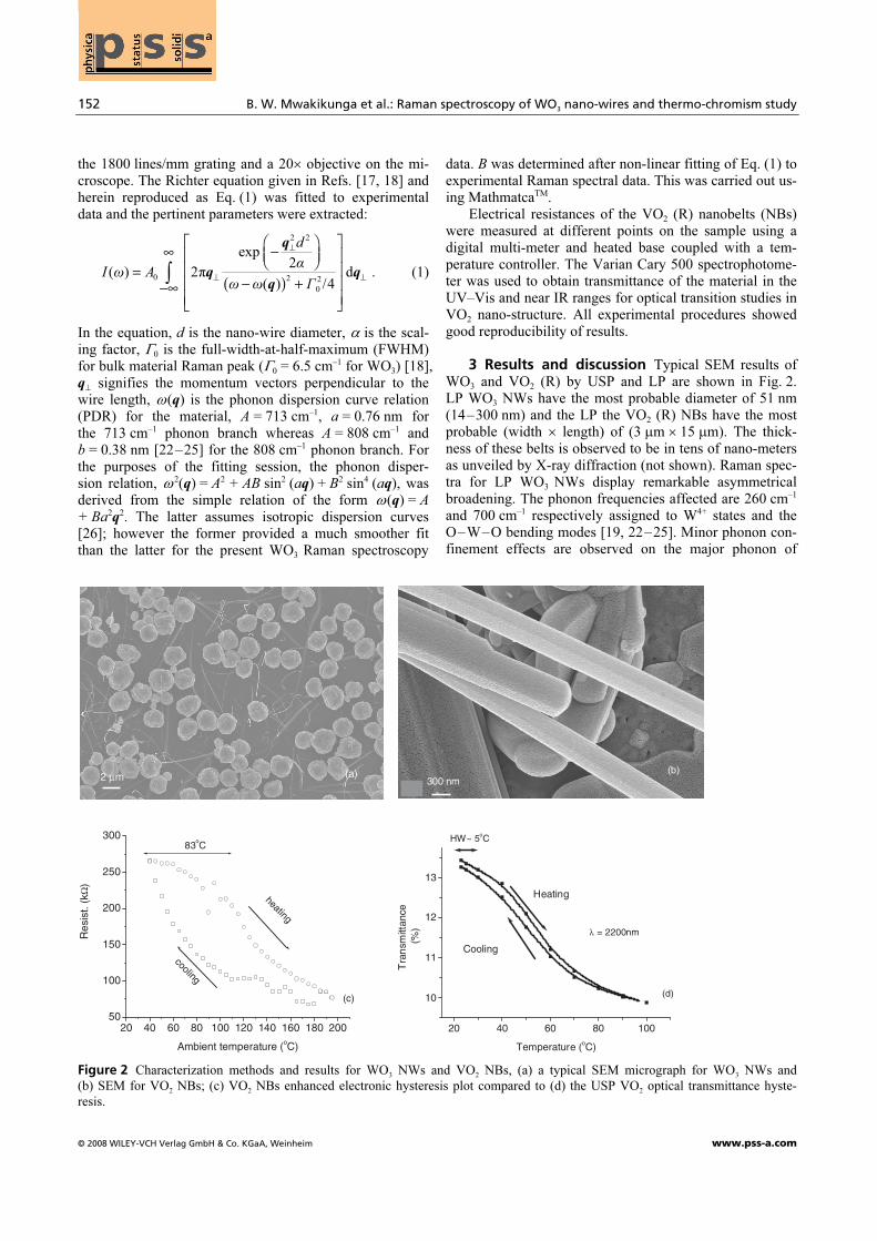
data. B was determined after non-linear fitting of Eq. (1) to experimental Raman spectral data. This was carried out us-ing MathmatcaTM. Electrical resistances of the VO2 (R) nanobelts (NBs) were measured at different points on the sample using a digital multi-meter and heated base coupled with a tem-perature controller. The Varian Cary 500 spectrophotome-ter was used to obtain transmittance of the material in the UV–Vis and near IR ranges for optical transition studies in VO2 nano-structure. All experimental procedures showed good reproducibility of results. 3 Results and discussion Typical SEM results of WO3 and VO2 (R) by USP and LP are shown in Fig. 2. LP WO3 NWs have the most probable diameter of 51 nm (14–300 nm) and the LP the VO2 (R) NBs have the most probable (width × length) of (3 µm × 15 µm). The thick-ness of these belts is observed to be in tens of nano-meters as unveiled by X-ray diffraction (not shown). Raman spec-tra for LP WO3 NWs display remarkable asymmetrical broadening. The phonon frequencies affected are 260 cm–1 and 700 cm–1 respectively assigned to W4+ states and the O–W–O bending modes [19, 22–25]. Minor phonon con-finement effects are observed on the major phonon of
(b)(b)
200nm200nm300 nm(b)
(b)(b)
200nm200nm300 nm
(b)(b)
200nm200nm300 nm200nm200nm300 nm(b)
2 µm (a)2 µm2 µm (a)
20 40 60 80 100 120 140 160 180 20050
100
150
200
250
300
(c)
83oC
cooling
heating
Res
ist.
(kΩ
)
Ambient temperature (oC)
20 40 60 80 100
10
11
12
13
(d)
λ = 2200nm
HW~ 5oC
Cooling
Heating
Tra
nsm
ittan
ce(%
)
Temperature (oC)
Figure 2 Characterization methods and results for WO3 NWs and VO
2 NBs, (a) a typical SEM micrograph for WO
3 NWs and
(b) SEM for VO2 NBs; (c) VO
2 NBs enhanced electronic hysteresis plot compared to (d) the USP VO
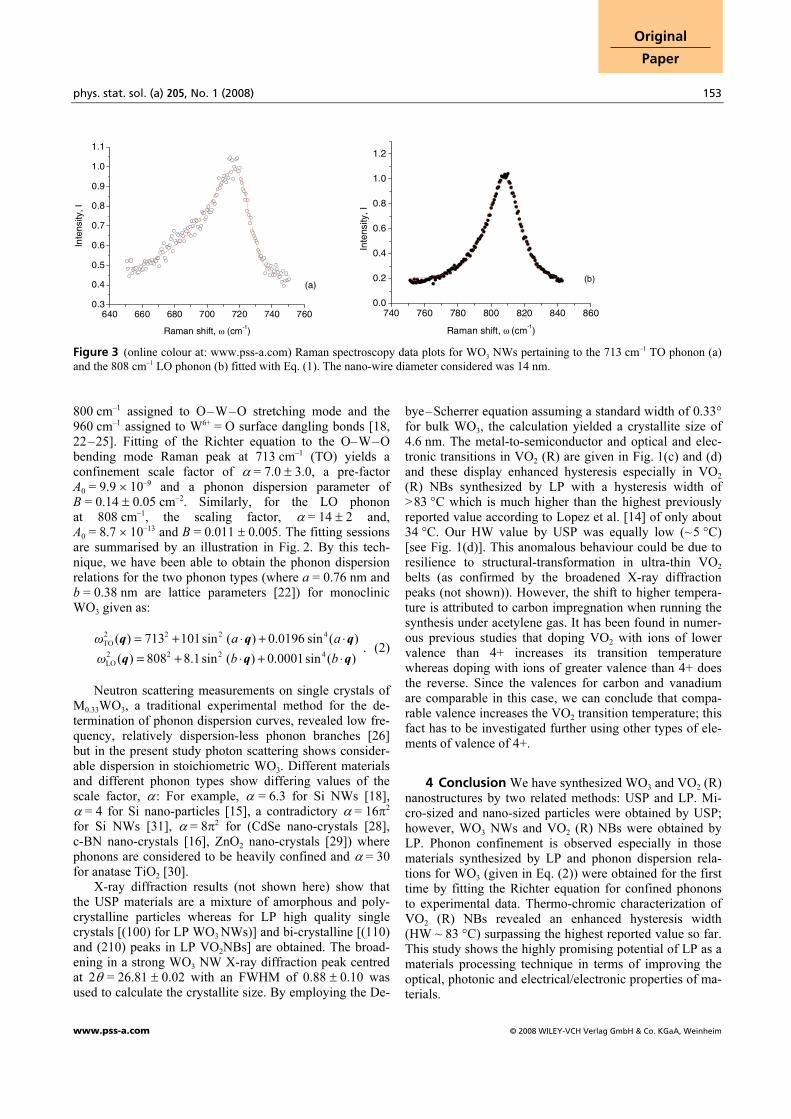
Figure 3 (online colour at: www.pss-a.com) Raman spectroscopy data plots for WO3 NWs pertaining to the 713 cm–1 TO phonon (a)
and the 808 cm–1 LO phonon (b) fitted with Eq. (1). The nano-wire diameter considered was 14 nm.
800 cm–1 assigned to O–W–O stretching mode and the 960 cm–1 assigned to W6+ = O surface dangling bonds [18, 22–25]. Fitting of the Richter equation to the O–W–O bending mode Raman peak at 713 cm–1 (TO) yields a confinement scale factor of α = 7.0 ± 3.0, a pre-factor A0 = 9.9 × 10⁻⁹ and a phonon dispersion parameter of B = 0.14 ± 0.05 cm–2. Similarly, for the LO phonon at 808 cm–1, the scaling factor, α = 14 ± 2 and, A0 = 8.7 × 10⁻¹³ and B = 0.011 ± 0.005. The fitting sessions are summarised by an illustration in Fig. 2. By this tech-nique, we have been able to obtain the phonon dispersion relations for the two phonon types (where a = 0.76 nm and b = 0.38 nm are lattice parameters [22]) for monoclinic WO3 given as:
2 2 2 4
TO
2 2 2 4
LO
( ) 713 101sin ( ) 0.0196 sin ( )
( ) 808 8.1sin ( ) 0.0001sin ( )
ω a a
ω b b
= + ◊ + ◊
= + ◊ + ◊
q q q
q q q . (2)
Neutron scattering measurements on single crystals of M0.33WO3, a traditional experimental method for the de-termination of phonon dispersion curves, revealed low fre-quency, relatively dispersion-less phonon branches [26] but in the present study photon scattering shows consider-able dispersion in stoichiometric WO3. Different materials and different phonon types show differing values of the scale factor, α : For example, α = 6.3 for Si NWs [18], α = 4 for Si nano-particles [15], a contradictory α = 16π2 for Si NWs [31], α = 8π2 for (CdSe nano-crystals [28], c-BN nano-crystals [16], ZnO2 nano-crystals [29]) where phonons are considered to be heavily confined and α = 30 for anatase TiO2 [30]. X-ray diffraction results (not shown here) show that the USP materials are a mixture of amorphous and poly-crystalline particles whereas for LP high quality single crystals [(100) for LP WO3 NWs)] and bi-crystalline [(110) and (210) peaks in LP VO2NBs] are obtained. The broad-ening in a strong WO3 NW X-ray diffraction peak centred at 2θ = 26.81 ± 0.02 with an FWHM of 0.88 ± 0.10 was used to calculate the crystallite size. By employing the De-
bye–Scherrer equation assuming a standard width of 0.33° for bulk WO3, the calculation yielded a crystallite size of 4.6 nm. The metal-to-semiconductor and optical and elec-tronic transitions in VO2 (R) are given in Fig. 1(c) and (d) and these display enhanced hysteresis especially in VO2 (R) NBs synthesized by LP with a hysteresis width of >83 °C which is much higher than the highest previously reported value according to Lopez et al. [14] of only about 34 °C. Our HW value by USP was equally low (~5 °C) [see Fig. 1(d)]. This anomalous behaviour could be due to resilience to structural-transformation in ultra-thin VO2 belts (as confirmed by the broadened X-ray diffraction peaks (not shown)). However, the shift to higher tempera-ture is attributed to carbon impregnation when running the synthesis under acetylene gas. It has been found in numer-ous previous studies that doping VO2 with ions of lower valence than 4+ increases its transition temperature whereas doping with ions of greater valence than 4+ does the reverse. Since the valences for carbon and vanadium are comparable in this case, we can conclude that compa-rable valence increases the VO2 transition temperature; this fact has to be investigated further using other types of ele-ments of valence of 4+.
4 Conclusion We have synthesized WO3 and VO2 (R) nanostructures by two related methods: USP and LP. Mi-cro-sized and nano-sized particles were obtained by USP; however, WO3 NWs and VO2 (R) NBs were obtained by LP. Phonon confinement is observed especially in those materials synthesized by LP and phonon dispersion rela-tions for WO3 (given in Eq. (2)) were obtained for the first time by fitting the Richter equation for confined phonons to experimental data. Thermo-chromic characterization of VO2 (R) NBs revealed an enhanced hysteresis width (HW ~ 83 °C) surpassing the highest reported value so far. This study shows the highly promising potential of LP as a materials processing technique in terms of improving the optical, photonic and electrical/electronic properties of ma-terials.
154 B. W. Mwakikunga et al.: Raman spectroscopy of WO3 nano-wires and thermo-chromism study
![This article has been published In Physica Status Solidi : Rapid … · 2020. 1. 24. · [15] This structural analogy between amorphous and crystal does clearly not hold for PCMs,](https://static.documents.pub/doc/80x56/60d48a2a57d11e1ca2173511/this-article-has-been-published-in-physica-status-solidi-rapid-2020-1-24.jpg)
![*,1 1,2 1 arXiv:1403.8015v1 [cond-mat.mes-hall] 31 Mar 2014 · 2018-10-08 · physica status solidi Towards combined transport and optical studies of the 0.7-anomaly in a quantum](https://static.documents.pub/doc/80x56/5e466d46324bc27c1c19c8b4/1-12-1-arxiv14038015v1-cond-matmes-hall-31-mar-2014-2018-10-08-physica.jpg)

![physica status solidi (a)) Volume 185 issue 1 2001 [doi 10.1002/1521-396x(200105)185:11::aid-pssa13.0.co;2-u] G. Müller; G. Krötz; J. Schalk -- New Sensors for Automotive and Aerospace](https://static.documents.pub/doc/80x56/577cdf061a28ab9e78b04f39/physica-status-solidi-a-volume-185-issue-1-2001-doi-1010021521-396x20010518511aid-pssa130co2-u.jpg)


