_______________________________________________________________ Maxim Integrated Products 1 For pricing, delivery, and ordering information, please contact Maxim Direct at 1-888-629-4642, or visit Maxim’s website at www.maxim-ic.com. MAX98306 Stereo 3.7W Class D Amplifier General Description The MAX98306 stereo 3.7W Class D amplifier provides Class AB audio performance with Class D efficiency. This device offers five selectable gain settings (6dB, 9dB, 12dB, 15dB, and 18dB) set by a single gain-select input (GAIN). Active emissions limiting, edge-rate, and overshoot con- trol circuitry combined with a filterless spread-spectrum modulation scheme (SSM) provide excellent EMI perfor- mance while eliminating the need for output filtering found in traditional Class D devices. These features reduce application component count. The IC's 2.0mA quiescent current with a 3.7V supply extends battery life in portable applications. The IC is available in a 14-pin TDFN (3mm x 3mm x 0.75mm) package specified over the extended -40NC to +85NC temperature range. Applications Features S Output Power 3.7W at 3I, 10% THD, 1.7W at 8I, 10% THD, with 5V Supply S Passes EMI Limit Unfiltered with Up to 12in of Speaker Cable S High 83dB PSRR at 217Hz S Spread-Spectrum Modulation and Active Emissions Limiting S Five Pin-Selectable Gains S Excellent Click-and-Pop Suppression S Thermal and Overcurrent Protection S Low-Current Shutdown Mode S Space-Saving, 3mm x 3mm x 0.75mm, 14-Pin TDFN 19-5919; Rev 1; 8/11 +Denotes a lead(Pb)-free/RoHS-compliant package. Ordering Information Typical Application Circuit Smartphones Tablets Cellular Phones Accessory Speakers MP3 Players Portable Audio Players VoIP Phones EVALUATION KIT AVAILABLE INL+ OUTL+ OUTL- OUTR- OUTR+ INL- INR- INR+ GAIN GAIN CONTROL 1μF 1μF 1μF 1μF PVDD PVDD PGND SHDN MAX98306 0.1μF 10μF +2.6V TO +5.5V PVDD PART TEMP RANGE PIN- PACKAGE TOP MARK MAX98306ETD+ -40NC to +85NC 14 TDFN +AEV
For pricing, delivery, and ordering information, please contact Maxim Direct at 1-888-629-4642, or visit Maxim’s website at www.maxim-ic.com.
MA
X9
83
06
Stereo 3.7W Class D Amplifier
General DescriptionThe MAX98306 stereo 3.7W Class D amplifier provides Class AB audio performance with Class D efficiency. This device offers five selectable gain settings (6dB, 9dB, 12dB, 15dB, and 18dB) set by a single gain-select input (GAIN).
Active emissions limiting, edge-rate, and overshoot con-trol circuitry combined with a filterless spread-spectrum modulation scheme (SSM) provide excellent EMI perfor-mance while eliminating the need for output filtering found in traditional Class D devices. These features reduce application component count.
The IC's 2.0mA quiescent current with a 3.7V supply extends battery life in portable applications.
The IC is available in a 14-pin TDFN (3mm x 3mm x 0.75mm) package specified over the extended -40NC to +85NC temperature range.
Applications
FeaturesS Output Power 3.7W at 3I, 10% THD, 1.7W at 8I,
10% THD, with 5V Supply
S Passes EMI Limit Unfiltered with Up to 12in of Speaker Cable
S High 83dB PSRR at 217Hz
S Spread-Spectrum Modulation and Active Emissions Limiting
Stresses beyond those listed under “Absolute Maximum Ratings” may cause permanent damage to the device. These are stress ratings only, and functional operation of the device at these or any other conditions beyond those indicated in the operational sections of the specifications is not implied. Exposure to absolute maximum rating conditions for extended periods may affect device reliability.
Voltage PVDD to PGND ....................................................-0.3V to +6VOUTL+, OUTR+, OUTL-, OUTR- to PGND ...........................................-0.3V to (VPVDD + 0.3V)All Other Pins to PGND .......................................-0.3V to +6V
Current Continuous Current Into/Out of PVDD, PGND, OUTL+, OUTR+, OUTL-, OUTR- .............................. ±800mAContinuous Input Current (all other pins) .................... ±20mA
Duration of Short Circuit OUTL+, OUTR+, OUTL-, OUTR- to PGND or PVDD ....ContinuousOUTL+ to OUTL- or OUTR+ to OUTR- ...................Continuous
Continuous Power Dissipation for a MultiLayer Board (TA = +70°C)TDFN (deration 24.4mW/°C above +70°C) ...............1951.2mW
Junction Temperature ....................................................+150°COperating Temperature Range ......................... -40°C to +85°CStorage Temperature Range .......................... -65°C to +150°CLead Temperature (10s, soldering) ...............................+300°CSoldering Temperature (reflow) ......................................+260°C
ELECTRICAL CHARACTERISTICS(VPVDD = VSHDN = 3.7V, VPGND = 0V, AV = 12dB (GAIN = PVDD), RL = J, RL connected between OUT_+ to OUT_-, 20Hz to 22kHz AC measurement bandwidth, TA = TMIN to TMAX, unless otherwise noted. Typical values are at TA = +25NC.) (Note 2)
ABSOLUTE MAXIMUM RATINGS
Note 1: Package thermal resistances were obtained using the method described in JEDEC specification JESD51-7, using a four-layer board. For detailed information on package thermal considerations, refer to www.maxim-ic.com/thermal-tutorial.
ELECTRICAL CHARACTERISTICS (continued)(VPVDD = VSHDN = 3.7V, VPGND = 0V, AV = 12dB (GAIN = PVDD), RL = J, RL connected between OUT_+ to OUT_-, 20Hz to 22kHz AC measurement bandwidth, TA = TMIN to TMAX, unless otherwise noted. Typical values are at TA = +25NC.) (Note 2)
PARAMETER SYMBOL CONDITIONS MIN TYP MAX UNITS
Click-and-Pop Level KCP
Peak voltage, TA = +25NC A-weighted, 32 samples per second (Notes 3, 4)
Into shutdown -79
dBVOut of shutdown -73
Power-Supply Rejection Ratio PSRRTA = +25NC (Note 3)
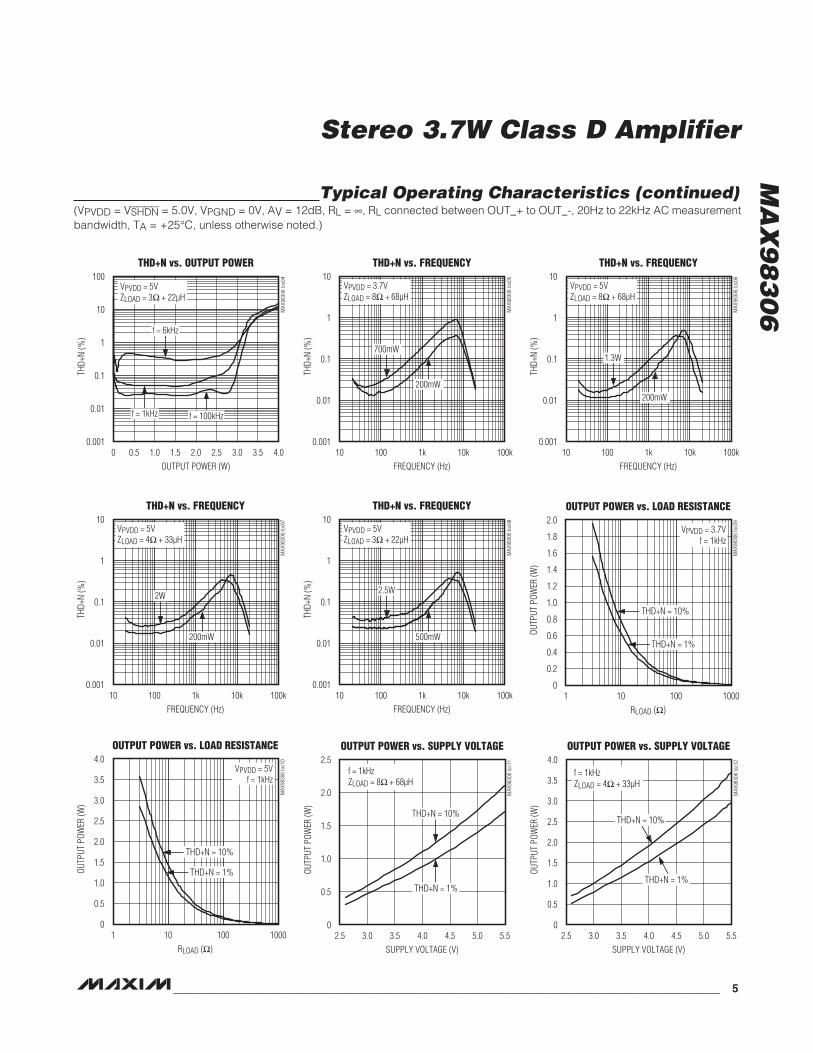
Typical Operating Characteristics(VPVDD = VSHDN = 5.0V, VPGND = 0V, AV = 12dB, RL = J, RL connected between OUT_+ to OUT_-, 20Hz to 22kHz AC measurement bandwidth, TA = +25NC, unless otherwise noted.)
ELECTRICAL CHARACTERISTICS (continued)(VPVDD = VSHDN = 3.7V, VPGND = 0V, AV = 12dB (GAIN = PVDD), RL = J, RL connected between OUT_+ to OUT_-, 20Hz to 22kHz AC measurement bandwidth, TA = TMIN to TMAX, unless otherwise noted. Typical values are at TA = +25NC.) (Note 2)
Note 2: This device is 100% production tested at TA = +25NC. All temperature limits are guaranteed by design.Note 3: Amplifier inputs AC-coupled to ground.Note 4: Specified at room temperature with an 8I resistive load in series with a 68µH inductive load.
THD+N vs. OUTPUT POWER
MAX
9830
6 to
c01
OUTPUT POWER (W)
THD+
N (%
)
0.750.500.25
0.01
0.1
1
10
100
0.0010 1.00
VPVDD = 3.7VZLOAD = 8I + 68µH
f = 6kHz
f = 1kHz
f = 100kHz
THD+N vs. OUTPUT POWER
MAX
9830
6 to
c02
OUTPUT POWER (W)
THD+
N (%
)
1.751.501.251.000.750.500.25
0.01
0.1
1
10
100
0.0010 2.00
VPVDD = 5VZLOAD = 8I + 68µH
f = 6kHz
f = 1kHz
f = 100kHz
THD+N vs. OUTPUT POWER
MAX
9830
6 to
c03
OUTPUT POWER (W)
THD+
N (%
)
3.02.52.01.51.00.5
0.01
0.1
1
10
100
0.0010 3.5
VPVDD = 5VZLOAD = 4I + 33µH
f = 6kHz
f = 1kHz f = 100kHz
PARAMETER SYMBOL CONDITIONS MIN TYP MAX UNITS
Signal-to-Noise Ratio SNR ZSPK = 8I +68FH, POUT at 1% THD+N 99 dB
Efficiency E ZSPK = 8I +68FH, POUT = 1.4W, f = 1kHz 92 %
Detailed DescriptionThe MAX98306 features low quiescent current, a low-power shutdown mode, comprehensive click-and-pop suppression, and excellent RF immunity.
The IC offers Class AB audio performance with Class D efficiency in a minimal board-space solution.
The Class D amplifier features spread-spectrum modula-tion, active emissions limiting, edge-rate, and overshoot control circuitry that offers significant improvements to switch-mode amplifier radiated emissions.
The amplifier also features click-and-pop suppression that reduces audible transients on startup and shut-down, as well as thermal-overload and short-circuit protection.
Class D Speaker AmplifierThe filterless Class D amplifier output stage offers much higher efficiency than Class AB amplifiers. The high effi-ciency of a Class D amplifier is due to the pulse-width modulated (PWM) rail-to-rail switching operation of the output stage transistors. This ensures that any power loss associated with the Class D output stage is mostly due to the I2R loss of the MOSFET on-resistance and quiescent current overhead.
EMI Filterless Output StageTraditional Class D amplifiers require the use of external LC filters, or shielding, to meet EN55022B electromag-netic-interference (EMI) regulation standards. Maxim’s active-emissions-limiting edge-rate control circuitry and spread-spectrum modulation reduce EMI emissions, while maintaining up to 92% efficiency.
Spread-spectrum modulation and active emissions limit-ing limit wideband spectral components, while propri-etary techniques ensure that the cycle-to-cycle varia-tion of the switching period does not degrade audio reproduction or efficiency. The IC’s spread-spectrum modulator randomly varies the switching frequency by Q20kHz around the center frequency (320kHz). Above 10MHz, the wideband spectrum looks like noise for EMI purposes (Figure 1).
Speaker Current LimitIf the output current of the speaker amplifier exceeds the current limit (3A typ), the IC disables the outputs for approximately 100Fs. At the end of 100Fs, the outputs are reenabled. If the fault condition still exists, the IC continues to disable and reenable the outputs until the fault condition is removed.
Selectable GainThe IC offers five programmable gains selected using the GAIN input.
ShutdownThe IC features a low-power shutdown mode, drawing P 1FA (typ) of supply current. Drive SHDN low to place the MAX98306 into shutdown. Drive SHDN above 1.4V for normal operation.
Click-and-Pop SuppressionThe IC speaker amplifier features Maxim’s comprehen-sive click-and-pop suppression. During startup, the click-and-pop suppression circuitry reduces any audible transient sources internal to the device. When entering shutdown, the differential speaker outputs ramp down to PGND quickly and simultaneously.
Table 1. Gain Control Configuration
Figure 1. EMI with 12in of Speaker Cable and No Output Filter
Applications InformationFilterless Class D Operation
Traditional Class D amplifiers require an output filter. The filter adds cost and size and decreases THD perfor-mance. The IC’s filterless modulation scheme does not require an output filter.
Because the switching frequency of the IC is well beyond the bandwidth of most speakers, voice coil movement due to the switching frequency is very small. Use a speaker with a series inductance > 10FH. Typical 8I speakers exhibit series inductances in the 20FH to 100FH range.
Component SelectionPower-Supply Input (PVDD)
PVDD powers the speaker amplifier. PVDD ranges from 2.6V to 5.5V. Bypass PVDD with 0.1FF and 10FF capaci-tors to PGND. Apply additional bulk capacitance at the device if long input traces between PVDD and the power source are used.
Input FilteringThe input-coupling capacitor (CIN), in conjunction with the amplifier’s internal input resistance (RIN), forms a highpass filter that removes the DC bias from the incom-ing signal. These capacitors allow the amplifier to bias the signal to an optimum DC level.
Assuming zero source impedance, CIN is:
−
=π ×IN
3dB IN
1C
2 f R
where f-3dB is the -3dB corner frequency and RIN is the typical value as specified in the Electrical Characteristics table. Use capacitors with adequately low-voltage coeffi-cients for best low-frequency THD performance. Table 2 shows calculated capacitance values based on a 20Hz highpass filter.
Layout and GroundingProper layout and grounding are essential for optimum performance. Good grounding improves audio perfor-mance and prevents switching noise from coupling into the audio signal.
Use wide, low-resistance output traces. As the load impedance decreases, the current drawn from the device increases. At higher current, the resistance of the output traces decrease the power delivered to the load. For example, if 2W is delivered from the device output to a 4I load through 100mI of total speaker trace, 1.904W is delivered to the speaker. If power is delivered through 10mI of total speaker trace, 1.99W is delivered to the speaker. Wide output, supply, and ground traces also improve the power dissipation of the device.
The IC is inherently designed for excellent RF immunity. For best performance, add ground fills around all signal traces on top or bottom PCB planes.
Chip InformationPROCESS: CMOS
Table 2. Capacitance Value for 20Hz Highpass Filter
Package InformationFor the latest package outline information and land patterns (footprints), go to www.maxim-ic.com/packages. Note that a “+”, “#”, or “-” in the package code indicates RoHS status only. Package drawings may show a different suffix character, but the drawing pertains to the package regardless of RoHS status.
Package Information (continued)For the latest package outline information and land patterns (footprints), go to www.maxim-ic.com/packages. Note that a “+”, “#”, or “-” in the package code indicates RoHS status only. Package drawings may show a different suffix character, but the drawing pertains to the package regardless of RoHS status.
Maxim cannot assume responsibility for use of any circuitry other than circuitry entirely embodied in a Maxim product. No circuit patent licenses are implied. Maxim reserves the right to change the circuitry and specifications without notice at any time.


![3727].pdf · Elite FM Stereo Tuner Stereo Pre-Amplifier CDP CD Pre-Amplifier CDS Compact Disc Player Owner's Manual](https://static.documents.pub/doc/80x56/5bb5abea09d3f2b63a8d384c/3727pdf-elite-fm-stereo-tuner-stereo-pre-amplifier-cdp-cd-pre-amplifier-cds.jpg)


